EP3671331A1 - Array substrate, method for manufacturing same, and display panel - Google Patents
Array substrate, method for manufacturing same, and display panel Download PDFInfo
- Publication number
- EP3671331A1 EP3671331A1 EP18846203.0A EP18846203A EP3671331A1 EP 3671331 A1 EP3671331 A1 EP 3671331A1 EP 18846203 A EP18846203 A EP 18846203A EP 3671331 A1 EP3671331 A1 EP 3671331A1
- Authority
- EP
- European Patent Office
- Prior art keywords
- transparent substrate
- light reflecting
- array substrate
- coarse region
- present disclosure
- Prior art date
- Legal status (The legal status is an assumption and is not a legal conclusion. Google has not performed a legal analysis and makes no representation as to the accuracy of the status listed.)
- Withdrawn
Links
- 239000000758 substrate Substances 0.000 title claims abstract description 120
- 238000000034 method Methods 0.000 title claims abstract description 19
- 238000004519 manufacturing process Methods 0.000 title claims abstract description 11
- 239000011241 protective layer Substances 0.000 claims description 26
- 239000000463 material Substances 0.000 claims description 18
- KRHYYFGTRYWZRS-UHFFFAOYSA-N Fluorane Chemical compound F KRHYYFGTRYWZRS-UHFFFAOYSA-N 0.000 claims description 8
- VEXZGXHMUGYJMC-UHFFFAOYSA-N Hydrochloric acid Chemical compound Cl VEXZGXHMUGYJMC-UHFFFAOYSA-N 0.000 claims description 8
- 239000011159 matrix material Substances 0.000 claims description 8
- 238000001312 dry etching Methods 0.000 claims description 7
- 239000011521 glass Substances 0.000 claims description 6
- 238000001039 wet etching Methods 0.000 claims description 6
- 229920002120 photoresistant polymer Polymers 0.000 claims description 5
- 238000000059 patterning Methods 0.000 claims description 4
- 239000000843 powder Substances 0.000 claims description 4
- 239000010410 layer Substances 0.000 description 10
- 230000000694 effects Effects 0.000 description 8
- 230000015572 biosynthetic process Effects 0.000 description 7
- 238000010586 diagram Methods 0.000 description 2
- 239000002184 metal Substances 0.000 description 2
- 239000007769 metal material Substances 0.000 description 2
- 230000003287 optical effect Effects 0.000 description 2
- 238000002161 passivation Methods 0.000 description 2
- 230000003044 adaptive effect Effects 0.000 description 1
- 238000010276 construction Methods 0.000 description 1
- 238000005516 engineering process Methods 0.000 description 1
- 230000014509 gene expression Effects 0.000 description 1
- 238000012986 modification Methods 0.000 description 1
- 230000004048 modification Effects 0.000 description 1
- 230000005855 radiation Effects 0.000 description 1
- 230000003313 weakening effect Effects 0.000 description 1
Images



Classifications
-
- G—PHYSICS
- G02—OPTICS
- G02F—OPTICAL DEVICES OR ARRANGEMENTS FOR THE CONTROL OF LIGHT BY MODIFICATION OF THE OPTICAL PROPERTIES OF THE MEDIA OF THE ELEMENTS INVOLVED THEREIN; NON-LINEAR OPTICS; FREQUENCY-CHANGING OF LIGHT; OPTICAL LOGIC ELEMENTS; OPTICAL ANALOGUE/DIGITAL CONVERTERS
- G02F1/00—Devices or arrangements for the control of the intensity, colour, phase, polarisation or direction of light arriving from an independent light source, e.g. switching, gating or modulating; Non-linear optics
- G02F1/01—Devices or arrangements for the control of the intensity, colour, phase, polarisation or direction of light arriving from an independent light source, e.g. switching, gating or modulating; Non-linear optics for the control of the intensity, phase, polarisation or colour
- G02F1/13—Devices or arrangements for the control of the intensity, colour, phase, polarisation or direction of light arriving from an independent light source, e.g. switching, gating or modulating; Non-linear optics for the control of the intensity, phase, polarisation or colour based on liquid crystals, e.g. single liquid crystal display cells
- G02F1/133—Constructional arrangements; Operation of liquid crystal cells; Circuit arrangements
- G02F1/1333—Constructional arrangements; Manufacturing methods
- G02F1/1335—Structural association of cells with optical devices, e.g. polarisers or reflectors
- G02F1/133553—Reflecting elements
-
- G—PHYSICS
- G02—OPTICS
- G02F—OPTICAL DEVICES OR ARRANGEMENTS FOR THE CONTROL OF LIGHT BY MODIFICATION OF THE OPTICAL PROPERTIES OF THE MEDIA OF THE ELEMENTS INVOLVED THEREIN; NON-LINEAR OPTICS; FREQUENCY-CHANGING OF LIGHT; OPTICAL LOGIC ELEMENTS; OPTICAL ANALOGUE/DIGITAL CONVERTERS
- G02F1/00—Devices or arrangements for the control of the intensity, colour, phase, polarisation or direction of light arriving from an independent light source, e.g. switching, gating or modulating; Non-linear optics
- G02F1/01—Devices or arrangements for the control of the intensity, colour, phase, polarisation or direction of light arriving from an independent light source, e.g. switching, gating or modulating; Non-linear optics for the control of the intensity, phase, polarisation or colour
- G02F1/13—Devices or arrangements for the control of the intensity, colour, phase, polarisation or direction of light arriving from an independent light source, e.g. switching, gating or modulating; Non-linear optics for the control of the intensity, phase, polarisation or colour based on liquid crystals, e.g. single liquid crystal display cells
- G02F1/133—Constructional arrangements; Operation of liquid crystal cells; Circuit arrangements
- G02F1/136—Liquid crystal cells structurally associated with a semi-conducting layer or substrate, e.g. cells forming part of an integrated circuit
- G02F1/1362—Active matrix addressed cells
- G02F1/136209—Light shielding layers, e.g. black matrix, incorporated in the active matrix substrate, e.g. structurally associated with the switching element
-
- H—ELECTRICITY
- H10—SEMICONDUCTOR DEVICES; ELECTRIC SOLID-STATE DEVICES NOT OTHERWISE PROVIDED FOR
- H10D—INORGANIC ELECTRIC SEMICONDUCTOR DEVICES
- H10D86/00—Integrated devices formed in or on insulating or conducting substrates, e.g. formed in silicon-on-insulator [SOI] substrates or on stainless steel or glass substrates
- H10D86/01—Manufacture or treatment
- H10D86/021—Manufacture or treatment of multiple TFTs
- H10D86/0212—Manufacture or treatment of multiple TFTs comprising manufacture, treatment or coating of substrates
-
- H—ELECTRICITY
- H10—SEMICONDUCTOR DEVICES; ELECTRIC SOLID-STATE DEVICES NOT OTHERWISE PROVIDED FOR
- H10D—INORGANIC ELECTRIC SEMICONDUCTOR DEVICES
- H10D86/00—Integrated devices formed in or on insulating or conducting substrates, e.g. formed in silicon-on-insulator [SOI] substrates or on stainless steel or glass substrates
- H10D86/40—Integrated devices formed in or on insulating or conducting substrates, e.g. formed in silicon-on-insulator [SOI] substrates or on stainless steel or glass substrates characterised by multiple TFTs
- H10D86/411—Integrated devices formed in or on insulating or conducting substrates, e.g. formed in silicon-on-insulator [SOI] substrates or on stainless steel or glass substrates characterised by multiple TFTs characterised by materials, geometry or structure of the substrates
-
- H—ELECTRICITY
- H10—SEMICONDUCTOR DEVICES; ELECTRIC SOLID-STATE DEVICES NOT OTHERWISE PROVIDED FOR
- H10D—INORGANIC ELECTRIC SEMICONDUCTOR DEVICES
- H10D86/00—Integrated devices formed in or on insulating or conducting substrates, e.g. formed in silicon-on-insulator [SOI] substrates or on stainless steel or glass substrates
- H10D86/40—Integrated devices formed in or on insulating or conducting substrates, e.g. formed in silicon-on-insulator [SOI] substrates or on stainless steel or glass substrates characterised by multiple TFTs
- H10D86/60—Integrated devices formed in or on insulating or conducting substrates, e.g. formed in silicon-on-insulator [SOI] substrates or on stainless steel or glass substrates characterised by multiple TFTs wherein the TFTs are in active matrices
-
- G—PHYSICS
- G02—OPTICS
- G02F—OPTICAL DEVICES OR ARRANGEMENTS FOR THE CONTROL OF LIGHT BY MODIFICATION OF THE OPTICAL PROPERTIES OF THE MEDIA OF THE ELEMENTS INVOLVED THEREIN; NON-LINEAR OPTICS; FREQUENCY-CHANGING OF LIGHT; OPTICAL LOGIC ELEMENTS; OPTICAL ANALOGUE/DIGITAL CONVERTERS
- G02F1/00—Devices or arrangements for the control of the intensity, colour, phase, polarisation or direction of light arriving from an independent light source, e.g. switching, gating or modulating; Non-linear optics
- G02F1/01—Devices or arrangements for the control of the intensity, colour, phase, polarisation or direction of light arriving from an independent light source, e.g. switching, gating or modulating; Non-linear optics for the control of the intensity, phase, polarisation or colour
- G02F1/13—Devices or arrangements for the control of the intensity, colour, phase, polarisation or direction of light arriving from an independent light source, e.g. switching, gating or modulating; Non-linear optics for the control of the intensity, phase, polarisation or colour based on liquid crystals, e.g. single liquid crystal display cells
- G02F1/133—Constructional arrangements; Operation of liquid crystal cells; Circuit arrangements
- G02F1/1333—Constructional arrangements; Manufacturing methods
- G02F1/1335—Structural association of cells with optical devices, e.g. polarisers or reflectors
- G02F1/13356—Structural association of cells with optical devices, e.g. polarisers or reflectors characterised by the placement of the optical elements
- G02F1/133565—Structural association of cells with optical devices, e.g. polarisers or reflectors characterised by the placement of the optical elements inside the LC elements, i.e. between the cell substrates
-
- G—PHYSICS
- G02—OPTICS
- G02F—OPTICAL DEVICES OR ARRANGEMENTS FOR THE CONTROL OF LIGHT BY MODIFICATION OF THE OPTICAL PROPERTIES OF THE MEDIA OF THE ELEMENTS INVOLVED THEREIN; NON-LINEAR OPTICS; FREQUENCY-CHANGING OF LIGHT; OPTICAL LOGIC ELEMENTS; OPTICAL ANALOGUE/DIGITAL CONVERTERS
- G02F2203/00—Function characteristic
- G02F2203/02—Function characteristic reflective
-
- G—PHYSICS
- G02—OPTICS
- G02F—OPTICAL DEVICES OR ARRANGEMENTS FOR THE CONTROL OF LIGHT BY MODIFICATION OF THE OPTICAL PROPERTIES OF THE MEDIA OF THE ELEMENTS INVOLVED THEREIN; NON-LINEAR OPTICS; FREQUENCY-CHANGING OF LIGHT; OPTICAL LOGIC ELEMENTS; OPTICAL ANALOGUE/DIGITAL CONVERTERS
- G02F2203/00—Function characteristic
- G02F2203/03—Function characteristic scattering
-
- H—ELECTRICITY
- H10—SEMICONDUCTOR DEVICES; ELECTRIC SOLID-STATE DEVICES NOT OTHERWISE PROVIDED FOR
- H10D—INORGANIC ELECTRIC SEMICONDUCTOR DEVICES
- H10D86/00—Integrated devices formed in or on insulating or conducting substrates, e.g. formed in silicon-on-insulator [SOI] substrates or on stainless steel or glass substrates
- H10D86/40—Integrated devices formed in or on insulating or conducting substrates, e.g. formed in silicon-on-insulator [SOI] substrates or on stainless steel or glass substrates characterised by multiple TFTs
- H10D86/441—Interconnections, e.g. scanning lines
Definitions
- the present disclosure relate to the field of display technologies, and in particular, to an array substrate, a method for manufacturing the same and a display panel thereof.
- Embodiments of the present disclosure provide an array substrate, a method for manufacturing the same, and a display panel thereof.
- an array substrate includes: a transparent substrate having a first side surface and a second side surface opposite to the first side surface; and a light reflecting structure disposed on the first side surface of the transparent substrate, wherein the second side surface of the transparent substrate has a coarse region, an orthographic projection of the coarse region on the transparent substrate coinciding with an orthographic projection of the light reflecting structure on the transparent substrate.
- the coarse region is a portion of a base material of the transparent substrate.
- the light reflecting structure includes a black matrix and a conductive structure.
- the conductive structure includes at least one of a data line, a data lead, a gate line, and a gate lead formed on the transparent substrate.
- the base material of the transparent substrate is glass.
- a display panel including the array substrate described in the first aspect of the embodiment of the present disclosure.
- a method for manufacturing an array substrate includes: providing a transparent substrate having a first side surface and a second side surface opposite to the first side surface, a light reflecting structure being disposed on the first side surface of the transparent substrate; and coarsening the second side surface of the transparent substrate to form a coarse region, wherein an orthographic projection of the coarse region on the transparent substrate coincides with an orthographic projection of the light reflecting structure on the transparent substrate.
- the coarse region is a portion of a base material of the transparent substrate.
- the coarsening includes: forming a protective layer on the second side surface of the transparent substrate; patterning the protective layer to form a patterned protective layer, wherein the patterned protective layer has an opening, an orthographic projection of the opening on the transparent substrate coinciding with an orthographic projection of the light reflecting structure on the transparent substrate; coarsening a portion, exposed by the opening, of the second side surface of the transparent substrate to form the coarse region; and removing the patterned protective layer.
- a material of the protective layer is a negative photoresist
- the patterning includes exposing the negative photoresist using the light reflecting structure as a mask.
- coarsening the portion, exposed by the opening, of the second side surface of the transparent substrate to form the coarse region includes a wet or dry etching.
- the base material of the transparent substrate is glass.
- the wet etching employs an etchant including frost powder, hydrofluoric acid, and hydrochloric acid.
- the dry etching employs a plasma of at least one of He, CF 4 , H 2 , and O 2 .
- the light reflecting structure includes a black matrix and a conductive structure.
- the conductive structure includes at least one of a data line, a data lead, a gate line, and a gate lead formed on the transparent substrate.
- FIG. 1 shows a display panel without a frame.
- a backlight module and an array substrate are respectively disposed on opposite sides of a color filter substrate.
- the array substrate is disposed on a display side.
- an array substrate is provided.
- a surface of a transparent substrate of the array substrate has a coarse region, which can reduce the reflection of ambient light caused by an undesired reflective structure (for example, a black matrix and a conductive structure) located on the transparent substrate, thereby improving the display effect of the display device.
- an undesired reflective structure for example, a black matrix and a conductive structure
- FIG. 2 is a schematic view showing a cross section of an array substrate according to an embodiment of the present disclosure.
- an array substrate 10 includes: a transparent substrate 1 having a first side surface 11 and a second side surface 12 opposite to the first side surface 11; and a plurality of light reflecting structures 2 located on the first side surface 11 of the transparent substrate 1.
- the second side surface 12 of the transparent substrate 1 has a plurality of coarse regions 13, an orthographic projection of the coarse region 13 on the transparent substrate 1 coinciding with an orthographic projection of the light reflecting structure 2 on the transparent substrate 1.
- the coarse region 13 is a portion of a surface of a base material of the transparent substrate 1.
- the base material of the transparent substrate 1 may be glass.
- the light reflecting structure 2 may include a black matrix and a conductive structure.
- the conductive structure may include at least one of a data line, a data lead, a gate line, and a gate lead formed on the transparent substrate 1.
- the light reflecting structure 2 may be made of a metal material.
- the light incident on the coarse region 13 is diffusely reflected due to the transparent substrate 1 has the coarse region 13, thereby weakening the reflection of ambient light along a certain direction on the light reflecting structure 2 and thus improving the display effect of the display device.
- FIG. 3 is a schematic structural view showing a display panel according to an embodiment of the present disclosure.
- the display panel 100 includes the array substrate 10 as shown in FIG. 1 , so that the display effect of the display panel 100 can be improved.
- a method for manufacturing an array substrate is provided. It is possible to manufacture an array substrate having a coarse region on a surface of a base material of a transparent substrate, thereby improving the display effect of the display device.
- FIG. 4 is a flow chart schematically showing a method for manufacturing an array substrate according to an embodiment of the present disclosure.
- a transparent substrate is provided; and in step S402, a protective layer is formed on a surface of the transparent substrate.
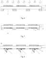
- FIG. 5 is a schematic view showing a cross section of formation of a protective layer according to an embodiment of the present disclosure.
- a transparent substrate 1 having a first side surface 11 and a second side surface 12 opposite to the first side surface 11 is provided, and a plurality of light reflecting structures 2 are disposed on the first side surface 11 of the transparent substrate 1.
- a protective layer 4 is formed on the second side surface 12 of the transparent substrate 1.
- FIG. 6 is a schematic view showing a cross section of formation of a patterned protective layer according to an embodiment of the present disclosure.
- the protective layer 4 is patterned to form a patterned protective layer 41.
- the protective layer 4 is exposed to radiation such as ultraviolet rays by using the light reflecting structure 2 as a mask.
- a material of the protective layer 4 is a negative photoresist.
- the patterned protective layer 41 has a plurality of openings 42, an orthographic projection of the opening 42 on the transparent substrate 1 coinciding with an orthographic projection of the light reflecting structure 2 on the transparent substrate 1.
- the light reflecting structure 2 may include a black matrix and a conductive structure.
- the conductive structure may include at least one of a data line, a data lead, a gate line, and a gate lead formed on the transparent substrate 1.
- the light reflecting structure 2 may be made of a metal material.
- FIG. 7 is a schematic view showing a cross section of formation of a coarse region according to an embodiment of the present disclosure.
- the second side surface 12 of the transparent substrate 1 is coarsened to form the coarse region 13.
- a portion, exposed by the opening 42, of the second side surface 12 of the transparent substrate 1 is coarsened to form the coarse region 13.
- the coarse region 13 is a portion of a surface of a base material of the transparent substrate 1.
- the base material of the transparent substrate 1 is glass.
- the above coarsening may include a wet or dry etching.
- the wet etching employs an etchant including frost powder, hydrofluoric acid, and hydrochloric acid.
- an etchant including frost powder, hydrofluoric acid, and hydrochloric acid.
- the frost powder, hydrofluoric acid, and hydrochloric acid are mixed to prepare an etchant, and the etchant is then applied (for example, sprayed) to at least a portion, exposed by the opening 42, of the second side surface 12 of the transparent substrate 1, the portion being sufficiently reacted with the etchant to form the coarse region 13.
- the dry etching employs a plasma of at least one of He, CF 4 , H 2 , and O 2 .
- a portion, exposed by the opening 42, of the second side surface 12 of the transparent substrate 1 is physically bombarded with a plasma of at least one of He, CF 4 , H 2 , and O 2 within a dry etching apparatus, thereby forming the coarse region 13.
- step S405 the patterned protective layer is removed. Specifically, the patterned protective layer 41 is removed, thereby manufacturing the array substrate 10 as shown in FIG. 2 .
- FIG. 8 is a view schematically showing a optical path of a reflected light when ambient light is incident on an array substrate according to an embodiment of the present disclosure.
- the light incident on the coarse region 13 is diffusely reflected so that ambient light is reflected in a plurality of directions, thereby reducing reflection of ambient light along a certain direction and thus improving the display effect of the display device.
- FIG. 9 a schematic view showing a cross section of an array substrate when the conductive structure includes a gate line and a gate lead.
- the array substrate 20 includes: a transparent substrate 1 having a first side surface 11 and a second side surface 12 opposite to the first side surface 11; a coarse region 13 located on the second side surface 12 on the transparent substrate 1; a gate line 21 and a gate lead 22 located on the first side surface 11 of the transparent substrate 1, a material of the gate line 21 and the gate lead 22 being a metal; a gate insulating layer 3 located on the first side surface 11, the gate line 21 and the gate lead 22; an active layer 6 and a source/drain electrode layer 7 located on the gate insulating layer 3; a passivation layer 5 located on the gate insulating layer 3, the active layer 6 and the source/drain electrode layer 7; and a conductive contact 8 connecting to the source/drain electrode layer 7 via a hole in the passivation layer 5.
- the transparent substrate 1 When ambient light is incident on the transparent substrate 1, the light is diffusely reflected on the coarse region 13, which can reduce the reflection of ambient light along a certain direction on the gate line 21 and the gate lead 22 made of metal, thereby improving the display effect of the display device including the array substrate 20.
- the surface of the base material of the transparent substrate of the array substrate has a coarse region, which can reduce the reflection of ambient light along a certain direction on the black matrix, the gate line, the gate lead, the data line, and the data lead, etc. on the transparent substrate, thereby improving the display effect of the display device.
Landscapes
- Physics & Mathematics (AREA)
- Nonlinear Science (AREA)
- Mathematical Physics (AREA)
- Chemical & Material Sciences (AREA)
- Crystallography & Structural Chemistry (AREA)
- General Physics & Mathematics (AREA)
- Optics & Photonics (AREA)
- Engineering & Computer Science (AREA)
- Microelectronics & Electronic Packaging (AREA)
- Devices For Indicating Variable Information By Combining Individual Elements (AREA)
Abstract
Description
- This application claims priority of China Patent Application No.
201710707687.6, filed on August 17, 2017 - The present disclosure relate to the field of display technologies, and in particular, to an array substrate, a method for manufacturing the same and a display panel thereof.
- At present, in order to increase the size of the display screen without increasing the size of the electronic device, more and more manufacturers are working on the display screen without a frame.
- Embodiments of the present disclosure provide an array substrate, a method for manufacturing the same, and a display panel thereof.
- According to a first aspect of an embodiment of the present disclosure, there is provided an array substrate. The array substrate includes: a transparent substrate having a first side surface and a second side surface opposite to the first side surface; and a light reflecting structure disposed on the first side surface of the transparent substrate, wherein the second side surface of the transparent substrate has a coarse region, an orthographic projection of the coarse region on the transparent substrate coinciding with an orthographic projection of the light reflecting structure on the transparent substrate.
- In an embodiment of the present disclosure, the coarse region is a portion of a base material of the transparent substrate.
- In an embodiment of the present disclosure, the light reflecting structure includes a black matrix and a conductive structure.
- In an embodiment of the present disclosure, the conductive structure includes at least one of a data line, a data lead, a gate line, and a gate lead formed on the transparent substrate.
- In an embodiment of the present disclosure, the base material of the transparent substrate is glass.
- According to a second aspect of an embodiment of the present disclosure, there is provided a display panel including the array substrate described in the first aspect of the embodiment of the present disclosure.
- According to a third aspect of embodiments of the present disclosure, there is provided a method for manufacturing an array substrate. The method includes: providing a transparent substrate having a first side surface and a second side surface opposite to the first side surface, a light reflecting structure being disposed on the first side surface of the transparent substrate; and coarsening the second side surface of the transparent substrate to form a coarse region, wherein an orthographic projection of the coarse region on the transparent substrate coincides with an orthographic projection of the light reflecting structure on the transparent substrate.
- In an embodiment of the present disclosure, the coarse region is a portion of a base material of the transparent substrate.
- In an embodiment of the present disclosure, the coarsening includes: forming a protective layer on the second side surface of the transparent substrate; patterning the protective layer to form a patterned protective layer, wherein the patterned protective layer has an opening, an orthographic projection of the opening on the transparent substrate coinciding with an orthographic projection of the light reflecting structure on the transparent substrate; coarsening a portion, exposed by the opening, of the second side surface of the transparent substrate to form the coarse region; and removing the patterned protective layer.
- In an embodiment of the present disclosure, a material of the protective layer is a negative photoresist, and the patterning includes exposing the negative photoresist using the light reflecting structure as a mask.
- In an embodiment of the present disclosure, coarsening the portion, exposed by the opening, of the second side surface of the transparent substrate to form the coarse region includes a wet or dry etching.
- In an embodiment of the present disclosure, the base material of the transparent substrate is glass.
- In an embodiment of the present disclosure, the wet etching employs an etchant including frost powder, hydrofluoric acid, and hydrochloric acid.
- In an embodiment of the present disclosure, the dry etching employs a plasma of at least one of He, CF4, H2, and O2.
- In an embodiment of the present disclosure, the light reflecting structure includes a black matrix and a conductive structure.
- In an embodiment of the present disclosure, the conductive structure includes at least one of a data line, a data lead, a gate line, and a gate lead formed on the transparent substrate.
- Adaptive and further aspects and scope will become apparent from the description provided herein. It should be understood that various aspects of this disclosure may be implemented individually or in combination with one or more other aspects. It should also be understood that the description and specific examples herein are intended for purposes of illustration only and are not intended to limit the scope of the present disclosure.
- The drawings described herein are for illustrative purposes only of selected embodiments and not all possible implementations, and are not intended to limit the scope of the present application.
-
FIG. 1 is a schematic view showing a cross section of a display panel without a frame; -
FIG. 2 is a schematic view showing a cross section of an array substrate according to an embodiment of the present disclosure; -
FIG. 3 is a schematic view showing a cross section of a display panel according to an embodiment of the present disclosure; -
FIG. 4 is a flow chart schematically showing a method for manufacturing an array substrate according to an embodiment of the present disclosure; -
FIG. 5 is a schematic cross-sectional view showing formation of a protective layer according to an embodiment of the present disclosure; -
FIG. 6 is a schematic cross-sectional view schematically showing formation of a patterned protective layer according to an embodiment of the present disclosure; -
FIG. 7 is a schematic cross-sectional view schematically showing formation of a coarse region according to an embodiment of the present disclosure; -
FIG. 8 is a view schematically showing a optical path of a reflected light when ambient light is incident on an array substrate according to an embodiment of the present disclosure; -
FIG. 9 is a schematic view showing a cross section of an array substrate according to an embodiment of the present disclosure. - Corresponding reference numerals indicate corresponding parts or features thcoarseout the several views of the drawings.
- As used herein and in the appended claims, the singular form of a word includes the plural, and vice versa, unless the context clearly dictates otherwise. Thus, the references "a", "an", and "the" are generally inclusive of the plurals of the respective terms. Similarly, the words "comprise", "comprises", and "comprising" are to be interpreted inclusively rather than exclusively. Likewise, the terms "include", "including" and "or" should all be construed to be inclusive, unless such a construction is clearly prohibited from the context. Where used herein the term "examples," particularly when followed by a listing of terms is merely exemplary and illustrative, and should not be deemed to be exclusive or comprehensive.
- Additionally, further to be noted, when the elements and the embodiments thereof of the present application are introduced, the articles "a/an", "one", "the" and "said" are intended to represent the existence of one or more elements. Unless otherwise specified, "a plurality of' means two or more. The expressions "comprise", "include", "contain" and "have" are intended as inclusive and mean that there may be other elements besides those listed. The terms such as "first" and "second" are used herein only for purposes of description and are not intended to indicate or imply relative importance and the order of formation.
- The flow diagrams depicted herein are just one example. There may be many variations to this diagram or the steps (or operations) described therein without departing from the spirit of the invention. For instance, the steps may be performed in a differing order or steps may be added, deleted or modified. All of these variations are considered a part of the claimed invention.
- Example embodiments will now be described more fully with reference to the accompanying drawings.
-
FIG. 1 shows a display panel without a frame. A backlight module and an array substrate are respectively disposed on opposite sides of a color filter substrate. The array substrate is disposed on a display side. When the ambient light is intense, reflection of light on the array substrate is strong, which causes a relatively obvious reflection, thereby affecting the display effect of the display device. - In an embodiment of the present disclosure, an array substrate is provided. A surface of a transparent substrate of the array substrate has a coarse region, which can reduce the reflection of ambient light caused by an undesired reflective structure (for example, a black matrix and a conductive structure) located on the transparent substrate, thereby improving the display effect of the display device.
-
FIG. 2 is a schematic view showing a cross section of an array substrate according to an embodiment of the present disclosure. As shown inFIG. 2 , anarray substrate 10 includes: atransparent substrate 1 having afirst side surface 11 and asecond side surface 12 opposite to thefirst side surface 11; and a plurality oflight reflecting structures 2 located on thefirst side surface 11 of thetransparent substrate 1. Thesecond side surface 12 of thetransparent substrate 1 has a plurality ofcoarse regions 13, an orthographic projection of thecoarse region 13 on thetransparent substrate 1 coinciding with an orthographic projection of thelight reflecting structure 2 on thetransparent substrate 1. In an embodiment of the present disclosure, thecoarse region 13 is a portion of a surface of a base material of thetransparent substrate 1. As an example, the base material of thetransparent substrate 1 may be glass. In an embodiment of the present disclosure, thelight reflecting structure 2 may include a black matrix and a conductive structure. As an example, the conductive structure may include at least one of a data line, a data lead, a gate line, and a gate lead formed on thetransparent substrate 1. In an embodiment of the present disclosure, thelight reflecting structure 2 may be made of a metal material. - In the embodiment of the present disclosure, when ambient light is incident on the
transparent substrate 1 of thearray substrate 10, the light incident on thecoarse region 13 is diffusely reflected due to thetransparent substrate 1 has thecoarse region 13, thereby weakening the reflection of ambient light along a certain direction on thelight reflecting structure 2 and thus improving the display effect of the display device. - In an embodiment of the present disclosure, a display panel is provided.
FIG. 3 is a schematic structural view showing a display panel according to an embodiment of the present disclosure. As shown inFIG. 3 , thedisplay panel 100 includes thearray substrate 10 as shown inFIG. 1 , so that the display effect of thedisplay panel 100 can be improved. - In an embodiment of the present disclosure, a method for manufacturing an array substrate is provided. It is possible to manufacture an array substrate having a coarse region on a surface of a base material of a transparent substrate, thereby improving the display effect of the display device.
-
FIG. 4 is a flow chart schematically showing a method for manufacturing an array substrate according to an embodiment of the present disclosure. As shown inFIG. 4 , in step S401, a transparent substrate is provided; and in step S402, a protective layer is formed on a surface of the transparent substrate.FIG. 5 is a schematic view showing a cross section of formation of a protective layer according to an embodiment of the present disclosure. As shown inFIG. 5 , atransparent substrate 1 having afirst side surface 11 and asecond side surface 12 opposite to thefirst side surface 11 is provided, and a plurality oflight reflecting structures 2 are disposed on thefirst side surface 11 of thetransparent substrate 1. Next, aprotective layer 4 is formed on thesecond side surface 12 of thetransparent substrate 1. - As shown in
FIG. 4 , in step S403, the protective layer is patterned.FIG. 6 is a schematic view showing a cross section of formation of a patterned protective layer according to an embodiment of the present disclosure. In the embodiment of the present disclosure, theprotective layer 4 is patterned to form a patternedprotective layer 41. Specifically, theprotective layer 4 is exposed to radiation such as ultraviolet rays by using thelight reflecting structure 2 as a mask. In an embodiment of the present disclosure, a material of theprotective layer 4 is a negative photoresist. In an embodiment of the present disclosure, the patternedprotective layer 41 has a plurality ofopenings 42, an orthographic projection of theopening 42 on thetransparent substrate 1 coinciding with an orthographic projection of thelight reflecting structure 2 on thetransparent substrate 1. - In an embodiment of the present disclosure, the
light reflecting structure 2 may include a black matrix and a conductive structure. As an example, the conductive structure may include at least one of a data line, a data lead, a gate line, and a gate lead formed on thetransparent substrate 1. In an embodiment of the present disclosure, thelight reflecting structure 2 may be made of a metal material. - As shown in
FIG. 4 , in step S404, a coarse region is formed.FIG. 7 is a schematic view showing a cross section of formation of a coarse region according to an embodiment of the present disclosure. In the embodiment of the present disclosure, thesecond side surface 12 of thetransparent substrate 1 is coarsened to form thecoarse region 13. Specifically, as shown inFIG. 7 , a portion, exposed by theopening 42, of thesecond side surface 12 of thetransparent substrate 1 is coarsened to form thecoarse region 13. In an embodiment of the present disclosure, thecoarse region 13 is a portion of a surface of a base material of thetransparent substrate 1. As an example, the base material of thetransparent substrate 1 is glass. In an embodiment of the present disclosure, the above coarsening may include a wet or dry etching. - As an example, the wet etching employs an etchant including frost powder, hydrofluoric acid, and hydrochloric acid. Specifically, the frost powder, hydrofluoric acid, and hydrochloric acid are mixed to prepare an etchant, and the etchant is then applied (for example, sprayed) to at least a portion, exposed by the
opening 42, of thesecond side surface 12 of thetransparent substrate 1, the portion being sufficiently reacted with the etchant to form thecoarse region 13. - As an example, the dry etching employs a plasma of at least one of He, CF4, H2, and O2. Specifically, a portion, exposed by the
opening 42, of thesecond side surface 12 of thetransparent substrate 1 is physically bombarded with a plasma of at least one of He, CF4, H2, and O2 within a dry etching apparatus, thereby forming thecoarse region 13.. - As shown in
FIG. 4 , in step S405, the patterned protective layer is removed. Specifically, the patternedprotective layer 41 is removed, thereby manufacturing thearray substrate 10 as shown inFIG. 2 . -
FIG. 8 is a view schematically showing a optical path of a reflected light when ambient light is incident on an array substrate according to an embodiment of the present disclosure. As shown inFIG. 8 , when ambient light is incident on thearray substrate 10, the light incident on thecoarse region 13 is diffusely reflected so that ambient light is reflected in a plurality of directions, thereby reducing reflection of ambient light along a certain direction and thus improving the display effect of the display device. -
FIG. 9 a schematic view showing a cross section of an array substrate when the conductive structure includes a gate line and a gate lead. As shown inFIG. 9 , thearray substrate 20 includes: atransparent substrate 1 having afirst side surface 11 and asecond side surface 12 opposite to thefirst side surface 11; acoarse region 13 located on thesecond side surface 12 on thetransparent substrate 1; agate line 21 and agate lead 22 located on thefirst side surface 11 of thetransparent substrate 1, a material of thegate line 21 and thegate lead 22 being a metal; agate insulating layer 3 located on thefirst side surface 11, thegate line 21 and thegate lead 22; anactive layer 6 and a source/drain electrode layer 7 located on thegate insulating layer 3; apassivation layer 5 located on thegate insulating layer 3, theactive layer 6 and the source/drain electrode layer 7; and a conductive contact 8 connecting to the source/drain electrode layer 7 via a hole in thepassivation layer 5. When ambient light is incident on thetransparent substrate 1, the light is diffusely reflected on thecoarse region 13, which can reduce the reflection of ambient light along a certain direction on thegate line 21 and thegate lead 22 made of metal, thereby improving the display effect of the display device including thearray substrate 20. - In an embodiment of the present disclosure, the surface of the base material of the transparent substrate of the array substrate has a coarse region, which can reduce the reflection of ambient light along a certain direction on the black matrix, the gate line, the gate lead, the data line, and the data lead, etc. on the transparent substrate, thereby improving the display effect of the display device.
- The foregoing description of the embodiment has been provided for purpose of illustration and description. It is not intended to be exhaustive or to limit the application. Individual elements or features of a particular embodiment are generally not limited to that particular embodiment, but, where applicable, are interchangeable and can be used in a selected embodiment, even if not specifically shown or described. The same may also be varied in many ways. Such variations are not to be regarded as a departure from the application, and all such modifications are included within the scope of the application.
Claims (16)
- An array substrate, comprising:a transparent substrate having a first side surface and a second side surface opposite to the first side surface; anda light reflecting structure disposed on the first side surface of the transparent substrate,wherein the second side surface of the transparent substrate has a coarse region, an orthographic projection of the coarse region on the transparent substrate coinciding with an orthographic projection of the light reflecting structure on the transparent substrate.
- The array substrate of claim 1, wherein the coarse region is a portion of a base material of the transparent substrate.
- The array substrate of claim 1, wherein the light reflecting structure comprises a black matrix and a conductive structure.
- The array substrate of claim 3, wherein the conductive structure comprises at least one of a data line, a data lead, a gate line, and a gate lead formed on the transparent substrate.
- The array substrate of claim 2, wherein the base material of the transparent substrate is glass.
- A display panel comprising the array substrate according to any one of claims 1 to 5.
- A method for manufacturing an array substrate, comprising:providing a transparent substrate having a first side surface and a second side surface opposite to the first side surface, a light reflecting structure being disposed on the first side surface of the transparent substrate; andcoarsening the second side surface of the transparent substrate to form a coarse region,wherein an orthographic projection of the coarse region on the transparent substrate coincides with an orthographic projection of the light reflecting structure on the transparent substrate.
- The method of claim 7, wherein the coarse region is a portion of a base material of the transparent substrate.
- The method of claim 7, wherein the coarsening comprises:forming a protective layer on the second side surface of the transparent substrate;patterning the protective layer to form a patterned protective layer, wherein the patterned protective layer has an opening, an orthographic projection of the opening on the transparent substrate coinciding with an orthographic projection of the light reflecting structure on the transparent substrate;coarsening a portion, exposed by the opening, of the second side surface of the transparent substrate to form the coarse region; andremoving the patterned protective layer.
- The method of claim 9, wherein a material of the protective layer is a negative photoresist, and the patterning comprises exposing the negative photoresist using the light reflecting structure as a mask.
- The method of claim 9, wherein coarsening the portion, exposed by the opening, of the second side surface of the transparent substrate to form the coarse region comprises a wet or dry etching.
- The method of claim 11, wherein the base material of the transparent substrate is glass.
- The method of claim 12, wherein the wet etching employs an etchant comprising frost powder, hydrofluoric acid, and hydrochloric acid.
- The method of claim 12, wherein the dry etching employs a plasma of at least one of He, CF4, H2, and O2.
- The method of claim 7, wherein the light reflecting structure comprises a black matrix and a conductive structure.
- The method of claim 15, wherein the conductive structure comprises at least one of a data line, a data lead, a gate line, and a gate lead formed on the transparent substrate.
Applications Claiming Priority (2)
| Application Number | Priority Date | Filing Date | Title |
|---|---|---|---|
| CN201710707687.6A CN109407431A (en) | 2017-08-17 | 2017-08-17 | Array substrate and preparation method thereof, display panel |
| PCT/CN2018/086872 WO2019033802A1 (en) | 2017-08-17 | 2018-05-15 | Array substrate, method for manufacturing same, and display panel |
Publications (2)
| Publication Number | Publication Date |
|---|---|
| EP3671331A1 true EP3671331A1 (en) | 2020-06-24 |
| EP3671331A4 EP3671331A4 (en) | 2021-05-19 |
Family
ID=65362676
Family Applications (1)
| Application Number | Title | Priority Date | Filing Date |
|---|---|---|---|
| EP18846203.0A Withdrawn EP3671331A4 (en) | 2017-08-17 | 2018-05-15 | Array substrate, method for manufacturing same, and display panel |
Country Status (4)
| Country | Link |
|---|---|
| US (1) | US20190355757A1 (en) |
| EP (1) | EP3671331A4 (en) |
| CN (1) | CN109407431A (en) |
| WO (1) | WO2019033802A1 (en) |
Families Citing this family (2)
| Publication number | Priority date | Publication date | Assignee | Title |
|---|---|---|---|---|
| CN110231730A (en) * | 2019-05-14 | 2019-09-13 | 深圳市华星光电技术有限公司 | The preparation method and color membrane substrates of color membrane substrates |
| CN112817485B (en) * | 2021-02-19 | 2022-09-23 | 联想(北京)有限公司 | Transparent cover plate and manufacturing method thereof |
Family Cites Families (24)
| Publication number | Priority date | Publication date | Assignee | Title |
|---|---|---|---|---|
| JP2002055333A (en) * | 2000-08-11 | 2002-02-20 | Seiko Epson Corp | Liquid crystal device substrate, method of manufacturing the same, liquid crystal device and electronic equipment |
| CN102081246A (en) * | 2009-12-01 | 2011-06-01 | 群康科技(深圳)有限公司 | Liquid crystal display panel and liquid crystal display device |
| TWI392919B (en) * | 2010-06-14 | 2013-04-11 | Au Optronics Corp | Liquid crystal display panel |
| CN102403320B (en) * | 2010-09-16 | 2015-05-20 | 上海天马微电子有限公司 | Array substrate, manufacturing method thereof and liquid crystal display panel |
| US20140051253A1 (en) * | 2012-08-14 | 2014-02-20 | Lam Research Corporation | Plasma baffle ring for a plasma processing apparatus and method of use |
| CN102955298A (en) * | 2012-11-16 | 2013-03-06 | 友达光电股份有限公司 | Liquid crystal display device |
| US8906810B2 (en) * | 2013-05-07 | 2014-12-09 | Lam Research Corporation | Pulsed dielectric etch process for in-situ metal hard mask shape control to enable void-free metallization |
| CN103346200A (en) * | 2013-05-13 | 2013-10-09 | 福建铂阳精工设备有限公司 | Glass substrate and method for manufacturing the same, and method for manufacturing thin-film solar cell |
| CN104724937A (en) * | 2013-12-23 | 2015-06-24 | 黄淼 | Environmentally friendly glass frosting paste |
| CN104297978B (en) * | 2014-10-30 | 2017-06-09 | 京东方科技集团股份有限公司 | A kind of preparation method of display base plate, the preparation method of display device |
| CN104464603A (en) * | 2014-12-30 | 2015-03-25 | 京东方科技集团股份有限公司 | Display panel and display device |
| CN104570445A (en) * | 2015-01-14 | 2015-04-29 | 京东方科技集团股份有限公司 | Display substrate and manufacturing method thereof, display device and manufacturing method thereof |
| CN104614911A (en) * | 2015-03-03 | 2015-05-13 | 京东方科技集团股份有限公司 | Substrate as well as manufacturing method and display device thereof |
| CN104829140B (en) * | 2015-05-26 | 2017-10-03 | 浙江星星科技股份有限公司 | A kind of anti-dazzle processing method of electronic product glass display screen |
| CN105118834B (en) * | 2015-07-17 | 2018-11-13 | 京东方科技集团股份有限公司 | Array substrate and preparation method thereof, display panel, display device |
| CN104977740A (en) * | 2015-07-29 | 2015-10-14 | 京东方科技集团股份有限公司 | Display substrate and preparation method thereof, and display apparatus |
| CN105470268A (en) * | 2016-01-11 | 2016-04-06 | 京东方科技集团股份有限公司 | Array substrate, fabrication method thereof and display device |
| CN105572998A (en) * | 2016-03-04 | 2016-05-11 | 京东方科技集团股份有限公司 | Array substrate, manufacturing method thereof and display device |
| CN205656403U (en) * | 2016-05-31 | 2016-10-19 | 上海天马微电子有限公司 | Array substrate, display panel and display device |
| CN106292102A (en) * | 2016-08-12 | 2017-01-04 | 京东方科技集团股份有限公司 | A kind of display floater and display |
| CN106292048A (en) * | 2016-09-18 | 2017-01-04 | 合肥鑫晟光电科技有限公司 | Display floater and preparation method thereof, display device |
| CN106684095B (en) * | 2016-10-31 | 2020-02-14 | 京东方科技集团股份有限公司 | Array substrate, preparation method thereof and display device |
| CN106835011B (en) * | 2016-12-20 | 2019-06-25 | 深圳先进技术研究院 | A kind of structural member with diamond-like carbon array and preparation method thereof |
| CN106547042B (en) * | 2017-01-25 | 2019-02-26 | 京东方科技集团股份有限公司 | Scattering film and array substrate having the same |
-
2017
- 2017-08-17 CN CN201710707687.6A patent/CN109407431A/en active Pending
-
2018
- 2018-05-15 US US16/331,285 patent/US20190355757A1/en not_active Abandoned
- 2018-05-15 EP EP18846203.0A patent/EP3671331A4/en not_active Withdrawn
- 2018-05-15 WO PCT/CN2018/086872 patent/WO2019033802A1/en not_active Ceased
Also Published As
| Publication number | Publication date |
|---|---|
| CN109407431A (en) | 2019-03-01 |
| US20190355757A1 (en) | 2019-11-21 |
| EP3671331A4 (en) | 2021-05-19 |
| WO2019033802A1 (en) | 2019-02-21 |
Similar Documents
| Publication | Publication Date | Title |
|---|---|---|
| US9709864B2 (en) | Array substrate and its manufacturing method and display device | |
| US10379413B2 (en) | Array substrate, manufacturing method thereof, and display apparatus | |
| US10175579B2 (en) | Mask, glass substrate and manufacturing method thereof | |
| US10658612B2 (en) | Display panel having passivation layer with protruding portions in peripheral area for sealant | |
| US10795228B2 (en) | Array substrate with diffuse reflection layer, method for manufacturing the same, and display device comprising the same | |
| EP3214492A1 (en) | Coa substrate and manufacturing method thereof and display device | |
| US20150340512A1 (en) | Thin film transistor, array substrate, method of fabricating same, and display device | |
| US20110063232A1 (en) | Projective-capacitive touch panel and fabrication method thereof | |
| KR20180056708A (en) | Liquid crystal display panel, array substrate and manufacturing method thereof | |
| US20160162080A1 (en) | Touch panel structure and method for manufacturing the same, and display apparatus and method for manufacturing the same | |
| US9483148B2 (en) | Method for manufacturing touch substrate | |
| US20170186879A1 (en) | Thin Film Transistor, Array Substrate and Manufacturing Processes of Them | |
| WO2017028455A1 (en) | Thin film transistor and manufacturing method thereof, array substrate and manufacturing method thereof, and display device | |
| CN115000146A (en) | Display panel, display device and preparation method of display panel | |
| CN114937681A (en) | Display panel, display device and preparation method of display panel | |
| CN107946318A (en) | A kind of array base palte and preparation method thereof, display panel | |
| US10177180B2 (en) | Method for forming pixel structure | |
| KR20160034381A (en) | Method for preventing metal lines in organic light emitting diode display device from short-circuit | |
| US20190355757A1 (en) | Array substrate, method for manufacturing the same, and display panel thereof | |
| EP3327778B1 (en) | Array substrate, preparation method thereof, display panel and display device | |
| WO2020207273A1 (en) | Display motherboard and manufacturing and cutting methods therefor, display substrate and device | |
| CN100447628C (en) | Method for manufacturing color filter layer | |
| US9841676B2 (en) | Method of manufacturing display device using bottom surface exposure | |
| US10310647B2 (en) | Touch-controlled panel, method of manufacturing the same, and display device | |
| CN113219749B (en) | Active element array substrate and display panel |
Legal Events
| Date | Code | Title | Description |
|---|---|---|---|
| STAA | Information on the status of an ep patent application or granted ep patent |
Free format text: STATUS: THE INTERNATIONAL PUBLICATION HAS BEEN MADE |
|
| PUAI | Public reference made under article 153(3) epc to a published international application that has entered the european phase |
Free format text: ORIGINAL CODE: 0009012 |
|
| STAA | Information on the status of an ep patent application or granted ep patent |
Free format text: STATUS: REQUEST FOR EXAMINATION WAS MADE |
|
| 17P | Request for examination filed |
Effective date: 20190304 |
|
| AK | Designated contracting states |
Kind code of ref document: A1 Designated state(s): AL AT BE BG CH CY CZ DE DK EE ES FI FR GB GR HR HU IE IS IT LI LT LU LV MC MK MT NL NO PL PT RO RS SE SI SK SM TR |
|
| AX | Request for extension of the european patent |
Extension state: BA ME |
|
| DAV | Request for validation of the european patent (deleted) | ||
| DAX | Request for extension of the european patent (deleted) | ||
| A4 | Supplementary search report drawn up and despatched |
Effective date: 20210419 |
|
| RIC1 | Information provided on ipc code assigned before grant |
Ipc: G02F 1/1335 20060101AFI20210413BHEP Ipc: G02F 1/1362 20060101ALI20210413BHEP |
|
| STAA | Information on the status of an ep patent application or granted ep patent |
Free format text: STATUS: THE APPLICATION HAS BEEN WITHDRAWN |
|
| 18W | Application withdrawn |
Effective date: 20220406 |