EP3671225A1 - Resistor having low temperature coefficient of resistance - Google Patents
Resistor having low temperature coefficient of resistance Download PDFInfo
- Publication number
- EP3671225A1 EP3671225A1 EP19218418.2A EP19218418A EP3671225A1 EP 3671225 A1 EP3671225 A1 EP 3671225A1 EP 19218418 A EP19218418 A EP 19218418A EP 3671225 A1 EP3671225 A1 EP 3671225A1
- Authority
- EP
- European Patent Office
- Prior art keywords
- resistor
- current direction
- main current
- slot
- sensing portion
- Prior art date
- Legal status (The legal status is an assumption and is not a legal conclusion. Google has not performed a legal analysis and makes no representation as to the accuracy of the status listed.)
- Pending
Links
Images





Classifications
-
- G—PHYSICS
- G01—MEASURING; TESTING
- G01R—MEASURING ELECTRIC VARIABLES; MEASURING MAGNETIC VARIABLES
- G01R1/00—Details of instruments or arrangements of the types included in groups G01R5/00 - G01R13/00 and G01R31/00
- G01R1/20—Modifications of basic electric elements for use in electric measuring instruments; Structural combinations of such elements with such instruments
- G01R1/203—Resistors used for electric measuring, e.g. decade resistors standards, resistors for comparators, series resistors, shunts
-
- H—ELECTRICITY
- H01—ELECTRIC ELEMENTS
- H01C—RESISTORS
- H01C3/00—Non-adjustable metal resistors made of wire or ribbon, e.g. coiled, woven or formed as grids
-
- G—PHYSICS
- G01—MEASURING; TESTING
- G01R—MEASURING ELECTRIC VARIABLES; MEASURING MAGNETIC VARIABLES
- G01R15/00—Details of measuring arrangements of the types provided for in groups G01R17/00 - G01R29/00, G01R33/00 - G01R33/26 or G01R35/00
- G01R15/14—Adaptations providing voltage or current isolation, e.g. for high-voltage or high-current networks
- G01R15/18—Adaptations providing voltage or current isolation, e.g. for high-voltage or high-current networks using inductive devices, e.g. transformers
-
- G—PHYSICS
- G01—MEASURING; TESTING
- G01R—MEASURING ELECTRIC VARIABLES; MEASURING MAGNETIC VARIABLES
- G01R19/00—Arrangements for measuring currents or voltages or for indicating presence or sign thereof
- G01R19/0092—Measuring current only
-
- H—ELECTRICITY
- H01—ELECTRIC ELEMENTS
- H01C—RESISTORS
- H01C1/00—Details
- H01C1/14—Terminals or tapping points specially adapted for resistors; Arrangements of terminals or tapping points on resistors
-
- H—ELECTRICITY
- H01—ELECTRIC ELEMENTS
- H01C—RESISTORS
- H01C1/00—Details
- H01C1/14—Terminals or tapping points specially adapted for resistors; Arrangements of terminals or tapping points on resistors
- H01C1/148—Terminals or tapping points specially adapted for resistors; Arrangements of terminals or tapping points on resistors the terminals embracing or surrounding the resistive element
-
- H—ELECTRICITY
- H01—ELECTRIC ELEMENTS
- H01C—RESISTORS
- H01C7/00—Non-adjustable resistors formed as one or more layers or coatings; Non-adjustable resistors made from powdered conducting material or powdered semi-conducting material with or without insulating material
- H01C7/06—Non-adjustable resistors formed as one or more layers or coatings; Non-adjustable resistors made from powdered conducting material or powdered semi-conducting material with or without insulating material including means to minimise changes in resistance with changes in temperature
Definitions
- the invention relates to a resistor having low temperature coefficient of resistance according to the pre-characterizing clause of claims 1 and 14.
- TCR Temperature Coefficient of Resistance
- most devices have a non-zero TCR that can lead to inaccurate sensing voltage readings at the sensing terminals particularly when the temperature of the device varies.
- the main terminals are usually made of copper. Copper has a TCR of 3900 ppm/°C while the resistive material is typically less than 100 ppm/°C, which makes the sensing terminals show a higher TCR than desired, resulting in significant deviation in monitoring the current passing through the device.
- the present invention aims at providing a resistor having low temperature coefficient of resistance, which uses an obstructing structure for reducing the sensing voltage deviation of a current passing through the resistor.
- a resistor having low temperature coefficient of resistance of an embodiment according to the invention includes a resistive part, a first conductive part, and a second conductive part.
- the resistor thereon defines a main current direction.
- the first conductive part is connected to a side of the resistive part in the main current direction.
- the first conductive part has a first sensing portion and a through slot.
- the first sensing portion is located between the through slot and the resistive part.
- the through slot includes a first slot section and a second slot section which are located at two opposite sides of the first sensing portion relative to the main current direction and connected with each other.
- the first slot section extends from a first start point along a first path toward the resistive part and ends with a closed end.
- the second slot section extends from the first start point along a second path toward the resistive part and ends with a closed end.
- the first path has a first parallel component, parallel to the main current direction, and a first perpendicular component, perpendicular to the main current direction.
- the second path has a second parallel component, parallel to the main current direction, and a second perpendicular component, perpendicular to the main current direction.
- the second conductive part is connected to another side of the resistive part in the main current direction.
- the second conductive part has a second sensing portion.
- a resistor having low temperature coefficient of resistance of another embodiment according to the invention includes a resistive part, a first conductive part, and a second conductive part.
- the resistor thereon defines a main current direction.
- the first conductive part is connected to a side of the resistive part in the main current direction.
- the first conductive part has a protrusion block extending outward perpendicular to the main current direction and ending with an end perpendicular to the main current direction.
- the first conductive part has a first sensing portion at the protrusion block.
- the second conductive part is connected to another side of the resistive part in the main current direction.
- the second conductive part has a second sensing portion.
- the first sensing portion and the second sensing portion are disposed at two sides of the resistive part respectively.
- the protrusion block forms an obstructing structure for reducing the sensing voltage deviation of a current passing through the resistor through the first sensing portion and the second sensing portion.
- a resistor 1 having low temperature coefficient of resistance includes a resistive part 12, a first conductive part 14, and a second conductive part 16.
- the resistor 1 thereon defines a main current direction D1 (indicated by an arrow in FIG. 1 ).
- the first conductive part 14 is connected to a side 12a of the resistive part 12 in the main current direction D1.
- the first conductive part 14 has a first sensing portion 142 (indicated by a circle in FIG. 1 ), a first through slot 144, and a first connecting portion 146 (indicated by a dashed circle in FIG. 1 ).
- the first sensing portion 142 is located between the first through slot 144 and the resistive part 12.
- the first through slot 144 is located between the first connecting portion 146 and the first sensing portion 142 along the main current direction D1.
- the second conductive part 16 is connected to another side 12b of the resistive part 12 opposite to the first conductive part 14 in the main current direction D1.
- the second conductive part 16 has a second sensing portion 162 (indicated by a circle in FIG. 1 ) and a second connecting portion 166 (indicated by a dashed circle in FIG. 1 ).
- a current passes through the resistor 1 substantially in the main current direction D1, for example form the first connecting portion 146 to the second connecting portion 166.
- the first through slot 144 is close to the first sensing portion 142 relative to the first connecting portion 146 and is located between the first connecting portion 146 and the first sensing portion 142, so that the first through slot 144 can obstruct the current and therefore can effectively reduce the sensing voltage deviation of the current through the first sensing portion 142 and the second sensing portion 162.
- the resistor 1 as a whole shows a plate form.
- the resistive part 12 can be made of, for example but not limited to an alloy of Cu, Ni, and Mn.
- the first conductive part 14 and the second conductive part 16 can be made of, for example but not limited to copper or an alloy of Cu.
- the resistive part 12 has a higher resistivity and a 10 times lower conductivity than the first conductive part 14 and the second conductive part 16; that is, the resistance of the resistive part 12 is 10 times larger than the resistance of the first conductive part 14 and the second conductive part 16.
- first sensing portion 142 and the second sensing portion 162 can be a solder pad or fix a pin or screw thereon or form a threaded hole for convenience of connecting with an external sensing circuit on PCB used for measuring the sensed voltages through the first sensing portion 142 and the second sensing portion 162.
- first connecting portion 146 and the second connecting portion 166 can be a solder pad or fix a pin or screw thereon or form a threaded hole for convenience of connecting with an external power unit for providing electric current (electric power) to the external power unit, e.g. battery, motor, motor driving unit, charger unit or control unit etc. passing through the resistors 1.
- the second conductive part 16 is connected to another side of the resistive part 12 rather than the opposite side 12b.
- the current will flow in accordance with this connection configuration, from the side 12a to said side.
- This connection configuration is suitable for curved installation space. In practice, this connection configuration may cause an uneven current density distribution, the sizes of the resistive part 12, the first conductive part 14 and the second conductive part 16 may need to be enlarged accordingly.
- the first through slot 144 includes a first slot section 1442 and a second slot section 1444 which are located at two opposite sides of the first sensing portion 142 relative to the main current direction D1 and connected with each other.
- the first slot section 1442 extends upward; the second slot section 1444 extends downward.
- the first slot section 1442 extends from a first start point S1 (indicated by a cross mark in FIG. 1 ) along a first path P1 (indicated by dashed lines with an arrow in FIG. 1 ) toward the resistive part 12 and ending with a closed end 1442a.
- the second slot section 1444 extends from the first start point S1 along a second path P2 (indicated by dashed lines with an arrow in FIG. 1 ) toward the resistive part 12 and ends with a closed end 1444a.
- the first path P1 has a first parallel component P11, parallel to the main current direction D1, and a first perpendicular component P12, perpendicular to the main current direction D1.
- the second path P2 has a second parallel component P21, parallel to the main current direction D1, and a second perpendicular component P22, perpendicular to the main current direction D1.
- the first parallel component P11, the first perpendicular component P12, the second parallel component P21, and the second perpendicular component P22 are nonzero.
- the first start point S1 (i.e. where the first slot section 1442 and the second slot section 1444 are connected) is located substantially on a line that passes through the first sensing portion 142 and the first connecting portion 146 parallel to the main current direction D1.
- the resistor 1 with the first through slot 144 as a whole has a lower TCR than the resistor 1 without the first through slot 144 as a whole.
- the resistor 1 has an indentation 122 formed at an edge of the resistive part 12, e.g. by laser trimming, milling, punching, or other methods capable of removing material from the resistor 1.
- the indentation 122 has a depth 122a selected to adjust the resistance of the resistor 1.
- the first through slot 144 as shown is provided in form of a square or rectangular bracket.
- the first slot section 1442 and the second slot section 1444 are symmetrical relative to the main current direction D1 or the first sensing portion 142, and are provided in form of an L-shape.
- the first through slot 144 of a resistor 1a can be provided in form of a C-shape, as shown by FIG. 2 ; therein, the first slot section 1442 and the second slot section 1444 are provided in form of an arc.
- the C-shape can be a semi-circle or an arc of a circle corresponding to a central angle of over 30 degrees (preferably, within a range of 30 to 330 degrees).
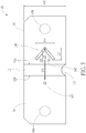
- the first through slot 144 of a resistor 1b can be formed in form of an angle bracket, as shown by FIG. 3 ; therein, the first slot section 1442 and the second slot section 1444 are provided in form of a straight line (or an oblique line).
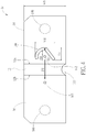
- the first slot section 1442 and the second slot section 1444 of the first through slot 144 of a resistor 1c are asymmetrical relative to the main current direction D1 or the first sensing portion 142, as shown by FIG. 4 ; therein, the first slot section 1442 is provided in form of an arc while the second slot section 1444 is provided in form of a straight line.
- the TCR of the resistors 1, 1a, 1b and 1c decrease as the projection lengths L1, L2, L3 and L4 of the first through slot 144 in the main current direction D1 increase.
- the TCR of the resistors 1, 1a, 1b and 1c also decrease as the projection lengths W1, W2, W3 and W4 of the first through slot 144 in a direction perpendicular to the main current direction D1 increase.
- the TCR of the resistors 1, 1a, 1b and 1c also decrease as the gap G1, G2, G3 and G4 between the first sensing portion 142 and the first through slot 144 (e.g. the distance between the first sensing portion 142 and the first start point S1) decrease.
- the sensing voltage of the resistors 1, 1a, 1b and 1c decrease as the projection lengths L1, L2, L3 and L4 of the first through slot 144 in the main current direction D1 increase.
- the sensing voltage of the resistors 1, 1a, 1b and 1c also decrease as the projection lengths W1, W2, W3 and W4 of the first through slot 144 in a direction perpendicular to the main current direction D1 increase. Under the same temperature, for maintaining the same sensing voltage (i.e. without changing the measurement deviation), it is necessary to increase the width W0, so that the size and cost of the resistors 1, 1a, 1b and 1c increases.
- the projection lengths W1, W2, W3 and W4 of the first through slot 144 can be designed to be less than a half of the width W0 of the first conductive part 14 in the direction perpendicular to the main current direction D1.
- the first connecting portion 146 may be formed with a structure in coordination with an external structure, e.g. for attaching a PCB or other attachments thereon.
- the first connecting portion 146 is a connecting hole (e.g. a simple hole or threaded hole).
- the first conductive part 14 has an extension through slot 148 that connects the first through slot 144 and the connecting hole (i.e. the connecting portion 146).
- the extension through slot 148 is also applicable to the resistor 1a, 1b and 1c, which will not be described in addition.
- a resistor 2 having low temperature coefficient of resistance is structurally similar to the resistor 1 and therefore uses the reference numbers of the resistor 1.
- the second conductive part 16 further has a second through slot 164.
- the second sensing portion 162 is located between the second through slot 164 and the resistive part 12; the second through slot 164 is located between the second connecting portion 166 and the second sensing portion 162 along the main current direction D1.
- the second through slot 164 includes a third slot section 1642 and a fourth slot section 1644 which are located at two opposite sides of the second sensing portion 162 relative to the main current direction D1 and connected with each other.
- the third slot section 1642 extends upward; the fourth slot section 1644 extends downward.
- the third slot section 1642 extends from a second start point S2 (indicated by a cross mark in FIG. 6 ) along a third path P3 (indicated by dashed lines with an arrow in FIG. 6 ) toward the resistive part 12 and ends with a closed end 1642a.
- the fourth slot section 1644 extends from the second start point S2 along a fourth path P4 (indicated by dashed lines with an arrow in FIG. 6 ) toward the resistive part 12 and ends with a closed end 1644a.
- the third path P3 has a third parallel component P31, parallel to the main current direction D1, and a third perpendicular component P32, perpendicular to the main current direction D1.
- the fourth path P4 has a fourth parallel component P41, parallel to the main current direction D1, and a fourth perpendicular component P42, perpendicular to the main current direction D1.
- the third parallel component P31, the third perpendicular component P32, the fourth parallel component P41, and the fourth perpendicular component P42 are nonzero.
- the second start point S2 (i.e. where the third slot section 1642 and the fourth slot section 1644 are connected) is located substantially on a line that passes through the second sensing portion 162 and the second connecting portion 166 parallel to the main current direction D1. Furthermore, in the embodiment, the first connecting portion 146, the first through slot 144, the first sensing portion 142, the resistive part 12, the second sensing portion 162, the second through slot 164, and the second connecting portion 166 are arranged in order in the main current direction D1.
- the current density at the first sensing portion 142 and the second sensing portion 1626 decreases, which reduces the sensing voltage deviation of the current passing through the resistor 2 through the first sensing portion 142 and the second sensing portion 162.
- the resistor 2 with the first through slot 144 and the second through slot 164 as a whole has a lower TCR than the resistor 2 without the first through slot 144 and the second through slot 164 as a whole.
- the resistor 1 has only one through slot (i.e. the first through slot 144) and therefore has relatively high heat-dissipation efficiency; in other words, when the resistors 1 and 2 are in operation, the resistor 1 has a lower operation temperature.
- the third slot section 1642 and the fourth slot section 1644 are symmetrical relative to the main current direction D1 or the second sensing portion 162.
- the first through slot 144 and the second through slot 164 are symmetrical relative to the resistive part 12.
- the first through slot 144 and the variations thereof are also applicable to the resistor 2.
- the second through slot 164 and variations therefor please refer to the relevant descriptions of the first through slot 144 and the variations thereof, which will not be repeated in addition.
- a resistor 3 having low temperature coefficient of resistance includes a resistive part 32, a first conductive part 34, and a second conductive part 36.
- the resistor 3 thereon defines a main current direction D2.
- the first conductive part 34 is connected to a side 32a of the resistive part 32 in the main current direction D2.
- the first conductive part 34 has a first protrusion block 342, which extends outward perpendicular to the main current direction D2 and ends with an end 342a perpendicular to the main current direction D2.
- the first conductive part 34 also has a first sensing portion 344 (indicated by a circle in FIG.
- the first protrusion block 342 is located between the first connecting portion 346 and the resistive part 32 in the main current direction D2.
- the second conductive part 36 is connected to another side 32b of the resistive part 32 relative to the first conductive part 34 in the main current direction D2.
- the second conductive part 36 is connected to another side of the resistive part 32 rather than the opposite side 32b. The current will flow in accordance with this connection configuration, from the side 32a to the another side.
- This connection configuration is suitable for curved installation space. In practice, this connection configuration may cause an uneven current density distribution, the sizes of the resistive part 32, the first conductive part 34 and the second conductive part 36 may need to be enlarged accordingly.
- the second conductive part 36 has a second protrusion block 362, which extends outward perpendicular to the main current direction D2 and ends with an end 362a perpendicular to the main current direction D2.
- the second conductive part 36 also has a second sensing portion 364 (indicated by a circle in FIG. 7 ) at the second protrusion block 362 (or at the end 362a), and a second connecting portion 366 (indicated by a dashed circle in FIG. 7 ).
- the second protrusion block 362 is located between the second connecting portion 366 and the resistive part 32 in the main current direction D2.
- the first protrusion block 342 and the second protrusion block 362 are oppositely disposed relative to the resistive part 32.
- a current passes through the resistor 3 substantially in the main current direction D2, for example form the first connecting portion 346 to the second connecting portion 366.
- An edge 342b of the first protrusion block 342 adjoins an edge 34a of the first conductive part 34, forming an obstructing structure located between the first sensing portion 344 and the first connecting portion 346 substantially in the main current direction D2; the obstructing structure can at least partially obstruct the flow of the current through the first protrusion block 342.
- an edge 362b of the second protrusion block 362 adjoins an edge 36a of the second conductive part 36, forming an obstructing structure located between the second sensing portion 364 and the second connecting portion 366 substantially in the main current direction D2; the obstructing structure can at least partially obstruct the flow of the current through the second protrusion block 362. Therefore, the obstructing structures can effectively reduce the sensing voltage deviation of the current through the first sensing portion 344 and the second sensing portion 364. In other words, the obstructing structures have the effect of reducing the TCR of the resistor 3.
- the resistor 3 has an indentation 322 formed at an edge of the resistive part 32 (opposite to the first protrusion block 342 and the second protrusion block 362 relative to the main current direction D2), e.g. by laser trimming, milling, punching, or other methods capable of removing material from the resistor 3.
- the indentation 322 has a depth 322a selected to adjust the resistance of the resistor 3.
- the resistive part 32 has a portion 324 between the first sensing portion 344 and the second sensing portion 364 (or between the first protrusion block 342 and the second protrusion block 362) in the main current direction D2; further, edges 324a, 342c and 362c of the resistive part 32, the first protrusion block 342, and the second protrusion block 362 are aligned.
- the portion 324 is located on a reference line segment (indicated by a dashed line in FIG. 7 ) from the first sensing portion 344 to the second sensing portion 364; the resistive part 32 has no hole structure along the line segment, so the current can flow along the line segment through the portion 324.
- a reference line segment indicated by a dashed line in FIG. 7
- the edge 34a (of the conductive part 34) or the edge 36a (of the second conductive part 36) is a straight edge (or a horizontal line in the view point of FIG. 7 ) extending parallel to the main current direction D2.
- the edge 34a or the edge 36a can be formed by a bottom edge of an indentation as shown by FIG. 8 .
- the edge 34a can be a slanted edge, extending obliquely relative to the main current direction D2, as shown by FIG. 9 .
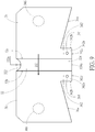
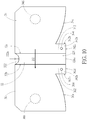
- the edge 34a can be a curved edge, extending obliquely relative to the main current direction D2, as shown by FIG. 10 .
- edge 34a is also applicable to the edge 36a of the second conductive part 36.
- the obstructing structures formed by the edges 34a, 342b, 36a and 362a
- the edges 34a, 342b, 36a and 362a can be provided easily by, but not limited to punching a metal plate.
- the resistor 3 can be surface-mounted to an external sensing circuit.
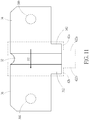
- the resistor 3 is surface-mounted to pads 42a and 42b (indicated by dashed lines in FIG. 11 ) of the external sensing circuit on a PCB (not shown in FIG. 11 ).
- the first protrusion block 342 and the second protrusion block 362 are directly mounted on the pads 42a and 42b respectively.
- the pads 42a and 42b extends to form leads 422a and 422b respectively as the sensing portions to be electrically connected to the external sensing circuit.
- the obstructing structures i.e. the first through slot 144 in the resistor 1 and the structure of the edges 34a and 342b in the resistor 3 for example
- the obstructing structures have the same or similar structural effect of at least partially obstructing the flow of the current through the resistors 1 and 3.
- the relevant descriptions of the components please refer to the relevant descriptions of the components with the same name of the resistor 1, which will not be repeated in addition.
- the resistors 1, 1a, 1b 1c, 2 and 3 are shown in symmetrical structures; however, it is not limited thereto in practice.
- a resistor 3a is structurally similar to the resistor 3. Only the first conductive part 34 of the resistor 3a has a protrusion block (i.e. the first protrusion block 342a) for disposing a sensing portion (i.e. the first sensing portion 344) thereon.
- the second sensing portion 364 of the second conductive part 36 and the first sensing portion 344 are disposed at the two sides of the resistive part 32 respectively.
- the obstructing structure which is formed by the edge 342b of the first protrusion block 342 adjoining the edge 34a of the first conductive part 34, is still conducive to reducing the sensing voltage deviation of the current through the first sensing portion 344 and the second sensing portion 364 in a certain degree. In other words, the obstructing structure still has the effect of reducing the TCR of the resistor 3a.
- the second conductive part 36 has a protrusion block 363 at another side of the second conductive part 36.
- the resistor 3a also can be provided with other sensing portions 344a and 364a (indicated by dashed circles in FIG. 12 ) on the first conductive part 34 and the second conductive part 36 respectively.
- an edge 363a of the protrusion block 363 and an edge 36b of the second conductive part 36 adjoin and form an obstructing structure located between the sensing portions 344a and 364a substantially in the main current direction D2. Therefore, the sensing portions 344a and 364a also can be used for sensing voltage like the sensing portions 344 and 364, which is conducive to the flexibility of disposition and design of the resistor 3a.
Landscapes
- Engineering & Computer Science (AREA)
- Microelectronics & Electronic Packaging (AREA)
- Physics & Mathematics (AREA)
- General Physics & Mathematics (AREA)
- Electromagnetism (AREA)
- Power Engineering (AREA)
- Details Of Resistors (AREA)
- Measuring Instrument Details And Bridges, And Automatic Balancing Devices (AREA)
- Apparatuses And Processes For Manufacturing Resistors (AREA)
Abstract
Description
- The invention relates to a resistor having low temperature coefficient of resistance according to the pre-characterizing clause of
claims - Current sense resistors have been available for the electronic market for many years. Their construction typically includes a flat strip of a resistive material that is coupled between high conductivity metal terminals forming the main terminals of the resistor. A pair of sensing terminals can be formed in the main terminals thereby creating a four terminal device. The main terminals carry the majority of the current through the resistor. The sensing terminals produce a sensing voltage that is proportional to the current passing through the resistor. Such resistors provide a mechanism to monitor the current using conventional voltage sensing techniques. The actual current passing through the resistor can be determined based on the sensed voltage and the resistance value of the resistor as dictated by ohms law. An ideal device would have a Temperature Coefficient of Resistance (TCR) that is close to zero. However, most devices have a non-zero TCR that can lead to inaccurate sensing voltage readings at the sensing terminals particularly when the temperature of the device varies. Furthermore, the main terminals are usually made of copper. Copper has a TCR of 3900 ppm/°C while the resistive material is typically less than 100 ppm/°C, which makes the sensing terminals show a higher TCR than desired, resulting in significant deviation in monitoring the current passing through the device.
- This in mind, the present invention aims at providing a resistor having low temperature coefficient of resistance, which uses an obstructing structure for reducing the sensing voltage deviation of a current passing through the resistor.
- This is achieved by a resistor having low temperature coefficient of resistance according to
claims - As will be seen more clearly from the detailed description following below, according to an embodiment, a resistor having low temperature coefficient of resistance of an embodiment according to the invention includes a resistive part, a first conductive part, and a second conductive part. The resistor thereon defines a main current direction. The first conductive part is connected to a side of the resistive part in the main current direction. The first conductive part has a first sensing portion and a through slot. The first sensing portion is located between the through slot and the resistive part. The through slot includes a first slot section and a second slot section which are located at two opposite sides of the first sensing portion relative to the main current direction and connected with each other. The first slot section extends from a first start point along a first path toward the resistive part and ends with a closed end. The second slot section extends from the first start point along a second path toward the resistive part and ends with a closed end. The first path has a first parallel component, parallel to the main current direction, and a first perpendicular component, perpendicular to the main current direction. The second path has a second parallel component, parallel to the main current direction, and a second perpendicular component, perpendicular to the main current direction. The second conductive part is connected to another side of the resistive part in the main current direction. The second conductive part has a second sensing portion. Thereby, the through slot can obstruct a current passing through the resistor so as to effectively reduce the sensing voltage deviation of the current through the first sensing portion and the second sensing portion.
- According to another embodiment, a resistor having low temperature coefficient of resistance of another embodiment according to the invention includes a resistive part, a first conductive part, and a second conductive part. The resistor thereon defines a main current direction. The first conductive part is connected to a side of the resistive part in the main current direction. The first conductive part has a protrusion block extending outward perpendicular to the main current direction and ending with an end perpendicular to the main current direction. The first conductive part has a first sensing portion at the protrusion block. The second conductive part is connected to another side of the resistive part in the main current direction. The second conductive part has a second sensing portion. The first sensing portion and the second sensing portion are disposed at two sides of the resistive part respectively. Thereby, the protrusion block forms an obstructing structure for reducing the sensing voltage deviation of a current passing through the resistor through the first sensing portion and the second sensing portion.
- In the following, the invention is further illustrated by way of example, taking reference to the accompanying drawings. Thereof:
-
FIG. 1 is a top view of a resistor of an embodiment according to the invention, -
FIG. 2 is a top view of a resistor with a C-shaped through slot of another embodiment, -
FIG. 3 is a top view of a resistor with an angle bracket through slot of another embodiment, -
FIG. 4 is a top view of a resistor with an arc-and-line through slot of another embodiment, -
FIG. 5 is a top view of a resistor with an attachment slot of another embodiment, -
FIG. 6 is a top view of a resistor of another embodiment according to the invention, -
FIG. 7 is a top view of a resistor of another embodiment according to the invention, -
FIG. 8 is a top view of a resistor with an indentation at the edge of the first connecting portion, -
FIG. 9 is a top view of a resistor with a slanted edge of another embodiment, -
FIG. 10 is a top view of a resistor with a curved edge of another embodiment, -
FIG. 11 is a top view of the resistor inFIG. 7 surface-mounted on pads in an application, and -
FIG. 12 is a top view of a resistor of another embodiment according to the invention. - Please refer to
FIG. 1 . Aresistor 1 having low temperature coefficient of resistance according to an embodiment includes aresistive part 12, a firstconductive part 14, and a secondconductive part 16. Theresistor 1 thereon defines a main current direction D1 (indicated by an arrow inFIG. 1 ). The firstconductive part 14 is connected to aside 12a of theresistive part 12 in the main current direction D1. The firstconductive part 14 has a first sensing portion 142 (indicated by a circle inFIG. 1 ), a first throughslot 144, and a first connecting portion 146 (indicated by a dashed circle inFIG. 1 ). Thefirst sensing portion 142 is located between the first throughslot 144 and theresistive part 12. The first throughslot 144 is located between the first connectingportion 146 and thefirst sensing portion 142 along the main current direction D1. The secondconductive part 16 is connected to anotherside 12b of theresistive part 12 opposite to the firstconductive part 14 in the main current direction D1. The secondconductive part 16 has a second sensing portion 162 (indicated by a circle inFIG. 1 ) and a second connecting portion 166 (indicated by a dashed circle inFIG. 1 ). When theresistor 1 is in operation, a current passes through theresistor 1 substantially in the main current direction D1, for example form the first connectingportion 146 to the second connectingportion 166. The first throughslot 144 is close to thefirst sensing portion 142 relative to the first connectingportion 146 and is located between the first connectingportion 146 and thefirst sensing portion 142, so that the first throughslot 144 can obstruct the current and therefore can effectively reduce the sensing voltage deviation of the current through thefirst sensing portion 142 and thesecond sensing portion 162. - In the embodiment, the
resistor 1 as a whole shows a plate form. In practice, theresistive part 12 can be made of, for example but not limited to an alloy of Cu, Ni, and Mn. The firstconductive part 14 and the secondconductive part 16 can be made of, for example but not limited to copper or an alloy of Cu. In principle, theresistive part 12 has a higher resistivity and a 10 times lower conductivity than the firstconductive part 14 and the secondconductive part 16; that is, the resistance of theresistive part 12 is 10 times larger than the resistance of the firstconductive part 14 and the secondconductive part 16. Furthermore, in practice, thefirst sensing portion 142 and thesecond sensing portion 162 can be a solder pad or fix a pin or screw thereon or form a threaded hole for convenience of connecting with an external sensing circuit on PCB used for measuring the sensed voltages through thefirst sensing portion 142 and thesecond sensing portion 162. Similarly, the first connectingportion 146 and the second connectingportion 166 can be a solder pad or fix a pin or screw thereon or form a threaded hole for convenience of connecting with an external power unit for providing electric current (electric power) to the external power unit, e.g. battery, motor, motor driving unit, charger unit or control unit etc. passing through theresistors 1. In addition, in some embodiments, the secondconductive part 16 is connected to another side of theresistive part 12 rather than theopposite side 12b. The current will flow in accordance with this connection configuration, from theside 12a to said side. This connection configuration is suitable for curved installation space. In practice, this connection configuration may cause an uneven current density distribution, the sizes of theresistive part 12, the firstconductive part 14 and the secondconductive part 16 may need to be enlarged accordingly. - Furthermore, in the embodiment, the first through
slot 144 includes afirst slot section 1442 and asecond slot section 1444 which are located at two opposite sides of thefirst sensing portion 142 relative to the main current direction D1 and connected with each other. In other words, in the view ofFIG. 1 , thefirst slot section 1442 extends upward; thesecond slot section 1444 extends downward. Thefirst slot section 1442 extends from a first start point S1 (indicated by a cross mark inFIG. 1 ) along a first path P1 (indicated by dashed lines with an arrow inFIG. 1 ) toward theresistive part 12 and ending with aclosed end 1442a. Thesecond slot section 1444 extends from the first start point S1 along a second path P2 (indicated by dashed lines with an arrow inFIG. 1 ) toward theresistive part 12 and ends with aclosed end 1444a. The first path P1 has a first parallel component P11, parallel to the main current direction D1, and a first perpendicular component P12, perpendicular to the main current direction D1. The second path P2 has a second parallel component P21, parallel to the main current direction D1, and a second perpendicular component P22, perpendicular to the main current direction D1. The first parallel component P11, the first perpendicular component P12, the second parallel component P21, and the second perpendicular component P22 are nonzero. In the embodiment, the first start point S1 (i.e. where thefirst slot section 1442 and thesecond slot section 1444 are connected) is located substantially on a line that passes through thefirst sensing portion 142 and the first connectingportion 146 parallel to the main current direction D1. - Because of the existence of the first through
slot 144 and the extension of two ends of the first throughslot 144 toward theresistive part 12, the current density at thefirst sensing portion 142 decreases, which reduces the sensing voltage deviation of the current passing through theresistor 1 through thefirst sensing portion 142 and thesecond sensing portion 162. In other words, theresistor 1 with the first throughslot 144 as a whole has a lower TCR than theresistor 1 without the first throughslot 144 as a whole. In addition, in the embodiment, theresistor 1 has anindentation 122 formed at an edge of theresistive part 12, e.g. by laser trimming, milling, punching, or other methods capable of removing material from theresistor 1. Theindentation 122 has adepth 122a selected to adjust the resistance of theresistor 1. - In the embodiment, the first through
slot 144 as shown is provided in form of a square or rectangular bracket. Thefirst slot section 1442 and thesecond slot section 1444 are symmetrical relative to the main current direction D1 or thefirst sensing portion 142, and are provided in form of an L-shape. However, it is not limited thereto in practice. For example, the first throughslot 144 of a resistor 1a can be provided in form of a C-shape, as shown byFIG. 2 ; therein, thefirst slot section 1442 and thesecond slot section 1444 are provided in form of an arc. In practice, the C-shape can be a semi-circle or an arc of a circle corresponding to a central angle of over 30 degrees (preferably, within a range of 30 to 330 degrees). For another example, the first throughslot 144 of aresistor 1b can be formed in form of an angle bracket, as shown byFIG. 3 ; therein, thefirst slot section 1442 and thesecond slot section 1444 are provided in form of a straight line (or an oblique line). For another example, thefirst slot section 1442 and thesecond slot section 1444 of the first throughslot 144 of a resistor 1c are asymmetrical relative to the main current direction D1 or thefirst sensing portion 142, as shown byFIG. 4 ; therein, thefirst slot section 1442 is provided in form of an arc while thesecond slot section 1444 is provided in form of a straight line. - Please refer to
FIG. 1 to FIG. 4 . In practice, the TCR of theresistors slot 144 in the main current direction D1 increase. The TCR of theresistors slot 144 in a direction perpendicular to the main current direction D1 increase. The TCR of theresistors first sensing portion 142 and the first through slot 144 (e.g. the distance between thefirst sensing portion 142 and the first start point S1) decrease. The sensing voltage of theresistors slot 144 in the main current direction D1 increase. The sensing voltage of theresistors slot 144 in a direction perpendicular to the main current direction D1 increase. Under the same temperature, for maintaining the same sensing voltage (i.e. without changing the measurement deviation), it is necessary to increase the width W0, so that the size and cost of theresistors conductive part 14, the projection lengths W1, W2, W3 and W4 of the first throughslot 144 can be designed to be less than a half of the width W0 of the firstconductive part 14 in the direction perpendicular to the main current direction D1. - In practice, the first connecting
portion 146 may be formed with a structure in coordination with an external structure, e.g. for attaching a PCB or other attachments thereon. As shown byFIG. 5 , the first connectingportion 146 is a connecting hole (e.g. a simple hole or threaded hole). The firstconductive part 14 has an extension throughslot 148 that connects the first throughslot 144 and the connecting hole (i.e. the connecting portion 146). The extension throughslot 148 is also applicable to theresistor 1a, 1b and 1c, which will not be described in addition. - Please refer to
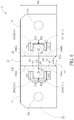
FIG. 6 . Aresistor 2 having low temperature coefficient of resistance according to another embodiment is structurally similar to theresistor 1 and therefore uses the reference numbers of theresistor 1. For other descriptions about theresistor 2, please refer to the relevant descriptions of theresistor 1 and the variations thereof, which will not be repeated in addition. Inresistor 2, the secondconductive part 16 further has a second throughslot 164. Thesecond sensing portion 162 is located between the second throughslot 164 and theresistive part 12; the second throughslot 164 is located between the second connectingportion 166 and thesecond sensing portion 162 along the main current direction D1. The second throughslot 164 includes athird slot section 1642 and afourth slot section 1644 which are located at two opposite sides of thesecond sensing portion 162 relative to the main current direction D1 and connected with each other. In other words, in the view ofFIG. 6 , thethird slot section 1642 extends upward; thefourth slot section 1644 extends downward. Thethird slot section 1642 extends from a second start point S2 (indicated by a cross mark inFIG. 6 ) along a third path P3 (indicated by dashed lines with an arrow inFIG. 6 ) toward theresistive part 12 and ends with aclosed end 1642a. Thefourth slot section 1644 extends from the second start point S2 along a fourth path P4 (indicated by dashed lines with an arrow inFIG. 6 ) toward theresistive part 12 and ends with aclosed end 1644a. The third path P3 has a third parallel component P31, parallel to the main current direction D1, and a third perpendicular component P32, perpendicular to the main current direction D1. The fourth path P4 has a fourth parallel component P41, parallel to the main current direction D1, and a fourth perpendicular component P42, perpendicular to the main current direction D1. The third parallel component P31, the third perpendicular component P32, the fourth parallel component P41, and the fourth perpendicular component P42 are nonzero. In the embodiment, the second start point S2 (i.e. where thethird slot section 1642 and thefourth slot section 1644 are connected) is located substantially on a line that passes through thesecond sensing portion 162 and the second connectingportion 166 parallel to the main current direction D1. Furthermore, in the embodiment, the first connectingportion 146, the first throughslot 144, thefirst sensing portion 142, theresistive part 12, thesecond sensing portion 162, the second throughslot 164, and the second connectingportion 166 are arranged in order in the main current direction D1. - Because of the existence of the first through
slot 144 and the second throughslot 164, and the extension of two ends of the first throughslot 144 and two ends of the second throughslot 164 toward theresistive part 12, the current density at thefirst sensing portion 142 and the second sensing portion 1626 decreases, which reduces the sensing voltage deviation of the current passing through theresistor 2 through thefirst sensing portion 142 and thesecond sensing portion 162. In other words, theresistor 2 with the first throughslot 144 and the second throughslot 164 as a whole has a lower TCR than theresistor 2 without the first throughslot 144 and the second throughslot 164 as a whole. In addition, compared to theresistor 2, theresistor 1 has only one through slot (i.e. the first through slot 144) and therefore has relatively high heat-dissipation efficiency; in other words, when theresistors resistor 1 has a lower operation temperature. - In addition, in the embodiment, the
third slot section 1642 and thefourth slot section 1644 are symmetrical relative to the main current direction D1 or thesecond sensing portion 162. The first throughslot 144 and the second throughslot 164 are symmetrical relative to theresistive part 12. However, it is not limited thereto in practice. Therefore, the first throughslot 144 and the variations thereof are also applicable to theresistor 2. For other descriptions about the second throughslot 164 and variations therefor, please refer to the relevant descriptions of the first throughslot 144 and the variations thereof, which will not be repeated in addition. - Please refer to
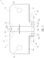
FIG. 7 . Aresistor 3 having low temperature coefficient of resistance according to an embodiment includes aresistive part 32, a firstconductive part 34, and a secondconductive part 36. Theresistor 3 thereon defines a main current direction D2. The firstconductive part 34 is connected to aside 32a of theresistive part 32 in the main current direction D2. The firstconductive part 34 has afirst protrusion block 342, which extends outward perpendicular to the main current direction D2 and ends with anend 342a perpendicular to the main current direction D2. The firstconductive part 34 also has a first sensing portion 344 (indicated by a circle inFIG. 7 ) at the first protrusion block 342 (or at theend 342a), and a first connecting portion 346 (indicated by a dashed circle inFIG. 7 ). Thefirst protrusion block 342 is located between the first connectingportion 346 and theresistive part 32 in the main current direction D2. The secondconductive part 36 is connected to anotherside 32b of theresistive part 32 relative to the firstconductive part 34 in the main current direction D2. In addition, in some embodiments, the secondconductive part 36 is connected to another side of theresistive part 32 rather than theopposite side 32b. The current will flow in accordance with this connection configuration, from theside 32a to the another side. This connection configuration is suitable for curved installation space. In practice, this connection configuration may cause an uneven current density distribution, the sizes of theresistive part 32, the firstconductive part 34 and the secondconductive part 36 may need to be enlarged accordingly. - In the embodiment, the second
conductive part 36 has asecond protrusion block 362, which extends outward perpendicular to the main current direction D2 and ends with anend 362a perpendicular to the main current direction D2. The secondconductive part 36 also has a second sensing portion 364 (indicated by a circle inFIG. 7 ) at the second protrusion block 362 (or at theend 362a), and a second connecting portion 366 (indicated by a dashed circle inFIG. 7 ). Thesecond protrusion block 362 is located between the second connectingportion 366 and theresistive part 32 in the main current direction D2. Thefirst protrusion block 342 and thesecond protrusion block 362 are oppositely disposed relative to theresistive part 32. - When the
resistor 3 is in operation, a current passes through theresistor 3 substantially in the main current direction D2, for example form the first connectingportion 346 to the second connectingportion 366. Anedge 342b of thefirst protrusion block 342 adjoins anedge 34a of the firstconductive part 34, forming an obstructing structure located between thefirst sensing portion 344 and the first connectingportion 346 substantially in the main current direction D2; the obstructing structure can at least partially obstruct the flow of the current through thefirst protrusion block 342. Similarly, anedge 362b of thesecond protrusion block 362 adjoins anedge 36a of the secondconductive part 36, forming an obstructing structure located between thesecond sensing portion 364 and the second connectingportion 366 substantially in the main current direction D2; the obstructing structure can at least partially obstruct the flow of the current through thesecond protrusion block 362. Therefore, the obstructing structures can effectively reduce the sensing voltage deviation of the current through thefirst sensing portion 344 and thesecond sensing portion 364. In other words, the obstructing structures have the effect of reducing the TCR of theresistor 3. - In the embodiment, the
resistor 3 has anindentation 322 formed at an edge of the resistive part 32 (opposite to thefirst protrusion block 342 and thesecond protrusion block 362 relative to the main current direction D2), e.g. by laser trimming, milling, punching, or other methods capable of removing material from theresistor 3. Theindentation 322 has adepth 322a selected to adjust the resistance of theresistor 3. Theresistive part 32 has aportion 324 between thefirst sensing portion 344 and the second sensing portion 364 (or between thefirst protrusion block 342 and the second protrusion block 362) in the main current direction D2; further,edges resistive part 32, thefirst protrusion block 342, and thesecond protrusion block 362 are aligned. Preferably, theportion 324 is located on a reference line segment (indicated by a dashed line inFIG. 7 ) from thefirst sensing portion 344 to thesecond sensing portion 364; theresistive part 32 has no hole structure along the line segment, so the current can flow along the line segment through theportion 324. However, it is not limited thereto in practice. - Furthermore, in the embodiment, the
edge 34a (of the conductive part 34) or theedge 36a (of the second conductive part 36) is a straight edge (or a horizontal line in the view point ofFIG. 7 ) extending parallel to the main current direction D2. In practice, theedge 34a or theedge 36a can be formed by a bottom edge of an indentation as shown byFIG. 8 . However, it is not limited thereto in practice. For example, theedge 34a can be a slanted edge, extending obliquely relative to the main current direction D2, as shown byFIG. 9 . For another example, theedge 34a can be a curved edge, extending obliquely relative to the main current direction D2, as shown byFIG. 10 . The above descriptions about the variations of theedge 34a are also applicable to theedge 36a of the secondconductive part 36. In addition, in practice, the obstructing structures (formed by theedges - In addition, in practice, the
resistor 3 can be surface-mounted to an external sensing circuit. For example, as shown byFIG. 11 , theresistor 3 is surface-mounted topads FIG. 11 ) of the external sensing circuit on a PCB (not shown inFIG. 11 ). Thefirst protrusion block 342 and thesecond protrusion block 362 are directly mounted on thepads pads - In the above embodiments, the obstructing structures (i.e. the first through
slot 144 in theresistor 1 and the structure of theedges resistor 3 for example) have the same or similar structural effect of at least partially obstructing the flow of the current through theresistors resistor 3 and variations therefor, please refer to the relevant descriptions of the components with the same name of theresistor 1, which will not be repeated in addition. - In addition, in the above embodiments, the
resistors 1b FIG. 12 , aresistor 3a is structurally similar to theresistor 3. Only the firstconductive part 34 of theresistor 3a has a protrusion block (i.e. thefirst protrusion block 342a) for disposing a sensing portion (i.e. the first sensing portion 344) thereon. Thesecond sensing portion 364 of the secondconductive part 36 and thefirst sensing portion 344 are disposed at the two sides of theresistive part 32 respectively. The obstructing structure, which is formed by theedge 342b of thefirst protrusion block 342 adjoining theedge 34a of the firstconductive part 34, is still conducive to reducing the sensing voltage deviation of the current through thefirst sensing portion 344 and thesecond sensing portion 364 in a certain degree. In other words, the obstructing structure still has the effect of reducing the TCR of theresistor 3a. Furthermore, in the embodiment, the secondconductive part 36 has aprotrusion block 363 at another side of the secondconductive part 36. Theresistor 3a also can be provided withother sensing portions FIG. 12 ) on the firstconductive part 34 and the secondconductive part 36 respectively. Anedge 363a of theprotrusion block 363 and anedge 36b of the secondconductive part 36 adjoin and form an obstructing structure located between thesensing portions sensing portions sensing portions resistor 3a. - Those skilled in the art will readily observe that numerous modifications and alterations of the device and method may be made while retaining the teachings of the invention. Accordingly, the above disclosure should be construed as limited only by the metes and bounds of the appended claims.
Claims (20)
- A resistor (1, 1a, 1b,1c,2) having low temperature coefficient of resistance, characterized by, the resistor (1, 1a, 1b,1c,2) thereon defining a main current direction (D1) and comprising:a resistive part (12);a first conductive part (14), connected to a side (12a) of the resistive part (12) in the main current direction (D1), the first conductive part (14) having a first sensing portion (142) and a first through slot (144), the first sensing portion (142) being located between the first through slot (144) and the resistive part (12), the first through slot (144) comprising a first slot section (1442) and a second slot section (1444) which are located at two opposite sides of the first sensing portion (142) relative to the main current direction (D1) and connected with each other, the first slot section (1442) extending from a first start point (SI) along a first path (P1) toward the resistive part (12) and ending with a closed end (1442a), the second slot section (1444) extending from the first start point (SI) along a second path (P2) toward the resistive part (12) and ending with a closed end (1642a), the first path (P1) having a first parallel component (P11), parallel to the main current direction (D1), and a first perpendicular component (P12), perpendicular to the main current direction (D1), the second path (P2) having a second parallel component (P21), parallel to the main current direction (D1), and a second perpendicular component (P22), perpendicular to the main current direction (D1); anda second conductive part (16), connected to another side (12b) of the resistive part (12) in the main current direction(D1), the second conductive part (16) having a second sensing portion (162).
- The resistor (1, 1a, 1b,2) of claim 1, characterized in that the first slot section (1442) and the second slot section (1444) are symmetrical relative to the main current direction (D1) or the first sensing portion (142).
- The resistor (1, 1a, 1b,1c,2) of claim 1, characterized in that the first through slot (144) has a projection length (W1,W2,W3,W4) in a direction perpendicular to the main current direction (D1), the first conductive part (14) has a width (W0) in the direction perpendicular to the main current direction (D1), and the projection length (W1,W2,W3,W4) is less than a half of the width (W0).
- The resistor (1, 1a, 1b,2) of claim 1, characterized in that the first through slot (144) is provided in form of a C-shape, a square bracket, rectangular bracket, or an angle bracket.
- The resistor (1, 1a, 1b,1c,2) of claim 1, characterized in that the first slot section (1442) is provided in form of an arc, an L-shape, or a straight line.
- The resistor of claim 1, characterized in that the first conductive part (14) has a connecting hole (146) and an extension through slot (148), and the extension through slot (148) connects the first through slot (144) and the connecting hole (146).
- The resistor (1, 1a, 1b,1c,2) of claim 1, characterized in that the first conductive part (14) has a first connecting portion (146), and the first through slot (144) is located between the first connecting portion (146) and the first sensing portion (142) along the main current direction (D1).
- The resistor (2) of claim 1, characterized in that the second conductive part (16) has a second through slot (164), and the second sensing portion (162) is located between the second through slot (164) and the resistive part (12).
- The resistor (2) of claim 8, characterized in that the second through slot (164) comprises a third slot section (1642) and a fourth slot section (1644) which are located at two opposite sides of the second sensing portion (162) relative to the main current direction (D1) and connected with each other, the third slot section (1642) extends from a second start point (S2) along a third path (P3) toward the resistive part (12) and ends with a closed end (1642a), the fourth slot section (1644) extends from the second start point (S2) along a fourth path (P4) toward the resistive part (12) and ends with a closed end (1644a), the third path (P3) has a third parallel component (P31), parallel to the main current direction (D1), and a third perpendicular component (P32), perpendicular to the main current direction (D1), and the fourth path (P4) has a fourth parallel component (P41), parallel to the main current direction (D1), and a fourth perpendicular component (P42), perpendicular to the main current direction (D1).
- The resistor (2) of claim 9, characterized in that the third slot section (1642) and the fourth slot section (1644) are symmetrical relative to the main current direction (D1) or the second sensing portion (162).
- The resistor (2) of claim 8, characterized in that the first through slot (144) and the second through slot (164) are symmetrical relative to the resistive part (12).
- The resistor (2) of claim 8, characterized in that the first conductive (14) has a first connecting portion (146), the second conductive (16) has a second connecting portion (166), and the first connecting portion (146), the first through slot (144), the first sensing portion (142), the resistive part (12), the second sensing portion (162), the second through slot (164), and the second connecting portion (166) are arranged in order in the main current direction (D1).
- The resistor (1, 1a, 1b,1c,2) of claim 1, characterized in that the resistive part (12) has an indentation (122), and the indentation (122) has a depth (122a) selected to adjust a resistance of the resistor (1, 1a, 1b,1c,2).
- A resistor (3,3a) having low temperature coefficient of resistance, characterized by, the resistor (3,3a) thereon defining a main current direction (D2), the resistor (3,3a) comprising:a resistive part (32);a first conductive part (34), connected to a side (32a) of the resistive part (32) in the main current direction (D2), the first conductive part (34) having a first protrusion block (342) extending outward perpendicular to the main current direction (D2) and ending with an end (324a) perpendicular to the main current direction (D2), the first conductive part (34) having a first sensing portion (344) at the first protrusion block (342); anda second conductive part (36), connected to another side (32b) of the resistive part (32) in the main current direction (32), the second conductive part (36) having a second sensing portion (364), the first sensing portion (344) and the second sensing portion (364) being disposed at the two sides (32a,32b) of the resistive part (32) respectively.
- The resistor (3,3a) of claim 14, characterized in that the first conductive part (34) has a straight edge (34a), and the straight edge (34a) extends parallel to the main current direction (D2) and adjoins an edge (342b) of the first protrusion block (342).
- The resistor of claim 14, characterized in that the first conductive part (34) has a slanted edge (34a), and the slanted edge (34a) extends obliquely relative to the main current direction (D2) and adjoins an edge (342b) of the first protrusion block (342).
- The resistor of claim 14, characterized in that the first conductive part (34) has a curved edge (34a), and the curved edge (34a) extends obliquely relative to the main current direction (D2) and adjoins an edge (342b) of the first protrusion block (342).
- The resistor (3,3a) of claim 14, characterized in that the resistive part (32) has a portion (324) located on a reference line segment from the first sensing portion (344) to the second sensing portion (364).
- The resistor (3) of claim 18, characterized in that the second conductive part (36) has a second protrusion block(362) extending outward perpendicular to the main current direction(D2) and ending with an end (362c) perpendicular to the main current direction (D2), the second sensing portion (364) is at the second protrusion block (362), the first protrusion block (342) and the second protrusion block (362) are disposed at the two sides (32a,32b) of the resistive part (32) respectively, and edges (324a,342c,362c) of the resistive part (32), and the first protrusion block (342), and the second protrusion block (362) are aligned.
- The resistor (3,3a) of claim 14, characterized in that the resistive part (32) has an indentation (322) at a side of the resistive part (32) opposite to the first protrusion block (342) relative to the main current direction (D2), and the indentation (322) has a depth (322a) selected to adjust a resistance of the resistor (3,3a).
Applications Claiming Priority (2)
| Application Number | Priority Date | Filing Date | Title |
|---|---|---|---|
| US201862783208P | 2018-12-21 | 2018-12-21 | |
| US16/708,349 US11415601B2 (en) | 2018-12-21 | 2019-12-09 | Resistor having low temperature coefficient of resistance |
Publications (1)
| Publication Number | Publication Date |
|---|---|
| EP3671225A1 true EP3671225A1 (en) | 2020-06-24 |
Family
ID=69005228
Family Applications (1)
| Application Number | Title | Priority Date | Filing Date |
|---|---|---|---|
| EP19218418.2A Pending EP3671225A1 (en) | 2018-12-21 | 2019-12-20 | Resistor having low temperature coefficient of resistance |
Country Status (5)
| Country | Link |
|---|---|
| US (1) | US11415601B2 (en) |
| EP (1) | EP3671225A1 (en) |
| JP (1) | JP7010921B2 (en) |
| CN (1) | CN111354523B (en) |
| TW (1) | TWI720743B (en) |
Cited By (5)
| Publication number | Priority date | Publication date | Assignee | Title |
|---|---|---|---|---|
| WO2022039808A1 (en) | 2020-08-20 | 2022-02-24 | Vishay Dale Electronics, Llc | Resistors, current sense resistors, battery shunts, shunt resistors, and methods of making |
| DE102021103241A1 (en) | 2021-02-11 | 2022-08-11 | Isabellenhütte Heusler Gmbh & Co. Kg | current sensing resistor |
| DE102021103238A1 (en) | 2021-02-11 | 2022-08-11 | Isabellenhütte Heusler Gmbh & Co. Kg | current sensing resistor |
| WO2022171439A1 (en) | 2021-02-11 | 2022-08-18 | Isabellenhütte Heusler Gmbh & Co. Kg | Current-sensing resistor |
| DE102021116419A1 (en) | 2021-06-24 | 2022-12-29 | Sma Solar Technology Ag | BUSBAR FOR CURRENT MEASUREMENT OF A DIRECT AND/OR AC CURRENT |
Families Citing this family (11)
| Publication number | Priority date | Publication date | Assignee | Title |
|---|---|---|---|---|
| CN102696079B (en) | 2009-09-04 | 2016-03-16 | 韦沙戴尔电子公司 | Resistors with Temperature Coefficient of Resistance (TCR) Compensation |
| DE102020101070B4 (en) * | 2020-01-17 | 2025-01-30 | Wieland & Munich Electrification Gmbh | Measuring circuit with a resistance arrangement and method for producing a band-shaped material composite for the resistance arrangement |
| EP4145471B1 (en) * | 2020-04-27 | 2025-07-02 | KOA Corporation | Shunt resistor, shunt resistor manufacturing method, and current detecting device |
| JP7491727B2 (en) * | 2020-04-28 | 2024-05-28 | Koa株式会社 | Shunt Resistor |
| DE102020118637B3 (en) | 2020-07-15 | 2022-01-13 | Isabellenhütte Heusler Gmbh & Co. Kg | Current measuring device with redundant current measurement |
| CN116868063A (en) * | 2021-02-11 | 2023-10-10 | 伊莎贝尔努特·霍伊斯勒两合公司 | Current sensing resistor |
| USD1069711S1 (en) | 2021-05-11 | 2025-04-08 | Vishay Dale Electronics, Llc | Resistor |
| JP7849964B2 (en) | 2021-12-14 | 2026-04-22 | Koa株式会社 | Shunt resistor and current detection device |
| CN116741482A (en) | 2022-03-01 | 2023-09-12 | 国巨电子(中国)有限公司 | Current sensing resistor and method of manufacturing same |
| JP7783770B2 (en) * | 2022-03-28 | 2025-12-10 | Koa株式会社 | Current detection device |
| DE102024211641A1 (en) * | 2024-12-05 | 2026-06-11 | Aumovio Germany Gmbh | Resistor assembly for a sensor device for determining an electric current |
Citations (3)
| Publication number | Priority date | Publication date | Assignee | Title |
|---|---|---|---|---|
| JP2007221006A (en) * | 2006-02-17 | 2007-08-30 | Sanken Electric Co Ltd | Resistor including resistance element and method of resistance value inspection performed by resistor |
| US20110057764A1 (en) * | 2009-09-04 | 2011-03-10 | Vishay Dale Electronics, Inc. | Resistor with temperature coefficient of resistance (tcr) compensation |
| WO2012019784A1 (en) * | 2010-08-26 | 2012-02-16 | Isabellenhütte Heusler Gmbh & Co. Kg | Current-sensing resistor |
Family Cites Families (14)
| Publication number | Priority date | Publication date | Assignee | Title |
|---|---|---|---|---|
| JPS5954204A (en) | 1982-09-21 | 1984-03-29 | 三洋電機株式会社 | Method of adjusting resistance value of chip resistor |
| JP4971693B2 (en) | 2006-06-09 | 2012-07-11 | コーア株式会社 | Metal plate resistor |
| US7477131B2 (en) * | 2006-09-07 | 2009-01-13 | E.I. Du Pont De Nemours | Low temperature coefficient of resistivity polymeric resistors based on metal carbides and nitrides |
| JP5263733B2 (en) | 2008-04-24 | 2013-08-14 | コーア株式会社 | Metal plate resistor |
| US9305687B2 (en) | 2010-05-13 | 2016-04-05 | Cyntec Co., Ltd. | Current sensing resistor |
| TWI428940B (en) | 2011-11-15 | 2014-03-01 | Ta I Technology Co Ltd | Current sensing resistor and method for manufacturing the same |
| JP6114905B2 (en) | 2012-08-28 | 2017-04-19 | パナソニックIpマネジメント株式会社 | Manufacturing method of chip resistor |
| WO2014203492A1 (en) * | 2013-06-20 | 2014-12-24 | 古河電気工業株式会社 | Battery state detection apparatus |
| CN104376938B (en) | 2013-08-13 | 2018-03-13 | 乾坤科技股份有限公司 | Resistance device |
| KR101537169B1 (en) * | 2013-11-26 | 2015-07-22 | 스마트전자 주식회사 | Current sensing resistor assembly |
| JP6305816B2 (en) | 2014-04-11 | 2018-04-04 | Koa株式会社 | Metal plate resistor |
| JP6370602B2 (en) * | 2014-05-09 | 2018-08-08 | Koa株式会社 | Current detection resistor |
| JP6622491B2 (en) | 2015-06-22 | 2019-12-18 | Koa株式会社 | Current detection device and manufacturing method thereof |
| JP6695122B2 (en) * | 2015-10-15 | 2020-05-20 | サンコール株式会社 | Manufacturing method of shunt resistor |
-
2019
- 2019-12-09 US US16/708,349 patent/US11415601B2/en active Active
- 2019-12-17 TW TW108146196A patent/TWI720743B/en active
- 2019-12-19 CN CN201911318853.9A patent/CN111354523B/en active Active
- 2019-12-20 EP EP19218418.2A patent/EP3671225A1/en active Pending
- 2019-12-20 JP JP2019230142A patent/JP7010921B2/en active Active
Patent Citations (3)
| Publication number | Priority date | Publication date | Assignee | Title |
|---|---|---|---|---|
| JP2007221006A (en) * | 2006-02-17 | 2007-08-30 | Sanken Electric Co Ltd | Resistor including resistance element and method of resistance value inspection performed by resistor |
| US20110057764A1 (en) * | 2009-09-04 | 2011-03-10 | Vishay Dale Electronics, Inc. | Resistor with temperature coefficient of resistance (tcr) compensation |
| WO2012019784A1 (en) * | 2010-08-26 | 2012-02-16 | Isabellenhütte Heusler Gmbh & Co. Kg | Current-sensing resistor |
Cited By (13)
| Publication number | Priority date | Publication date | Assignee | Title |
|---|---|---|---|---|
| EP4197011A4 (en) * | 2020-08-20 | 2024-03-06 | Vishay Dale Electronics, LLC | Resistors, current sense resistors, battery shunts, shunt resistors, and methods of making |
| WO2022039808A1 (en) | 2020-08-20 | 2022-02-24 | Vishay Dale Electronics, Llc | Resistors, current sense resistors, battery shunts, shunt resistors, and methods of making |
| EP4291906B1 (en) | 2021-02-11 | 2024-12-25 | Isabellenhütte Heusler GmbH & Co. KG | Current-sensing resistor |
| WO2022171427A1 (en) | 2021-02-11 | 2022-08-18 | Isabellenhütte Heusler Gmbh & Co. Kg | Current-sensing resistor |
| WO2022171439A1 (en) | 2021-02-11 | 2022-08-18 | Isabellenhütte Heusler Gmbh & Co. Kg | Current-sensing resistor |
| DE102021103238A1 (en) | 2021-02-11 | 2022-08-11 | Isabellenhütte Heusler Gmbh & Co. Kg | current sensing resistor |
| DE102021103241A1 (en) | 2021-02-11 | 2022-08-11 | Isabellenhütte Heusler Gmbh & Co. Kg | current sensing resistor |
| US12282042B2 (en) | 2021-02-11 | 2025-04-22 | Isabellenhütte Heusler Gmbh & Co. Kg | Current-sensing resistor |
| US12372555B2 (en) | 2021-02-11 | 2025-07-29 | Isabellenhütte Heusler Gmbh & Co. Kg | Current-sensing resistor |
| DE102021116419A1 (en) | 2021-06-24 | 2022-12-29 | Sma Solar Technology Ag | BUSBAR FOR CURRENT MEASUREMENT OF A DIRECT AND/OR AC CURRENT |
| WO2022269069A1 (en) * | 2021-06-24 | 2022-12-29 | Sma Solar Technology Ag | Busbar for measuring a direct and/or alternating current |
| US20240110945A1 (en) * | 2021-06-24 | 2024-04-04 | Sma Solar Technology Ag | Busbar for measuring a direct and/or alternating current |
| US12663440B2 (en) * | 2021-06-24 | 2026-06-23 | Sma Solar Technology Ag | Busbar for measuring a direct and/or alternating current |
Also Published As
| Publication number | Publication date |
|---|---|
| US20200200799A1 (en) | 2020-06-25 |
| JP7010921B2 (en) | 2022-01-26 |
| CN111354523A (en) | 2020-06-30 |
| US11415601B2 (en) | 2022-08-16 |
| CN111354523B (en) | 2022-12-27 |
| TWI720743B (en) | 2021-03-01 |
| JP2020102626A (en) | 2020-07-02 |
| TW202029228A (en) | 2020-08-01 |
Similar Documents
| Publication | Publication Date | Title |
|---|---|---|
| US11415601B2 (en) | Resistor having low temperature coefficient of resistance | |
| EP4145471B1 (en) | Shunt resistor, shunt resistor manufacturing method, and current detecting device | |
| US9035736B2 (en) | Magnetic device having integrated current sensing element and methods of assembling same | |
| CN104115241B (en) | Resistor terminal connection structure | |
| JP7627172B2 (en) | Current Detector | |
| US12249445B2 (en) | Shunt resistor | |
| CN116264120B (en) | Shunt resistor and current detection device | |
| JP4403428B2 (en) | Printed wiring board | |
| JP2002372551A (en) | Mounting structure of current detection resistor | |
| CN104078194B (en) | Magnetic devices and its assemble method with integrated current sensing element | |
| CN104376938B (en) | Resistance device | |
| WO2023112438A1 (en) | Shunt resistor and current detection device | |
| JP2007078599A (en) | Resistor for current detection and control device | |
| JP2009212253A (en) | Current detection resistor | |
| JP3006313B2 (en) | Shunt resistance device | |
| JPH0543502U (en) | Resistor for current detection | |
| KR20060008686A (en) | Terminal part installation structure of electronic parts |
Legal Events
| Date | Code | Title | Description |
|---|---|---|---|
| PUAI | Public reference made under article 153(3) epc to a published international application that has entered the european phase |
Free format text: ORIGINAL CODE: 0009012 |
|
| STAA | Information on the status of an ep patent application or granted ep patent |
Free format text: STATUS: THE APPLICATION HAS BEEN PUBLISHED |
|
| AK | Designated contracting states |
Kind code of ref document: A1 Designated state(s): AL AT BE BG CH CY CZ DE DK EE ES FI FR GB GR HR HU IE IS IT LI LT LU LV MC MK MT NL NO PL PT RO RS SE SI SK SM TR |
|
| AX | Request for extension of the european patent |
Extension state: BA ME |
|
| STAA | Information on the status of an ep patent application or granted ep patent |
Free format text: STATUS: REQUEST FOR EXAMINATION WAS MADE |
|
| 17P | Request for examination filed |
Effective date: 20201221 |
|
| RBV | Designated contracting states (corrected) |
Designated state(s): AL AT BE BG CH CY CZ DE DK EE ES FI FR GB GR HR HU IE IS IT LI LT LU LV MC MK MT NL NO PL PT RO RS SE SI SK SM TR |
|
| STAA | Information on the status of an ep patent application or granted ep patent |
Free format text: STATUS: EXAMINATION IS IN PROGRESS |
|
| 17Q | First examination report despatched |
Effective date: 20230130 |