EP3671187A1 - Photonic sensor chip, packaged photonic sensor device and arrangement - Google Patents
Photonic sensor chip, packaged photonic sensor device and arrangement Download PDFInfo
- Publication number
- EP3671187A1 EP3671187A1 EP19218716.9A EP19218716A EP3671187A1 EP 3671187 A1 EP3671187 A1 EP 3671187A1 EP 19218716 A EP19218716 A EP 19218716A EP 3671187 A1 EP3671187 A1 EP 3671187A1
- Authority
- EP
- European Patent Office
- Prior art keywords
- photonic
- active
- sensor chip
- photonic sensor
- semiconductor substrate
- Prior art date
- Legal status (The legal status is an assumption and is not a legal conclusion. Google has not performed a legal analysis and makes no representation as to the accuracy of the status listed.)
- Granted
Links
Images





Classifications
-
- G—PHYSICS
- G02—OPTICS
- G02B—OPTICAL ELEMENTS, SYSTEMS OR APPARATUS
- G02B6/00—Light guides; Structural details of arrangements comprising light guides and other optical elements, e.g. couplings
- G02B6/10—Light guides; Structural details of arrangements comprising light guides and other optical elements, e.g. couplings of the optical waveguide type
- G02B6/12—Light guides; Structural details of arrangements comprising light guides and other optical elements, e.g. couplings of the optical waveguide type of the integrated circuit kind
- G02B6/122—Basic optical elements, e.g. light-guiding paths
- G02B6/1225—Basic optical elements, e.g. light-guiding paths comprising photonic band-gap structures or photonic lattices
-
- G—PHYSICS
- G01—MEASURING; TESTING
- G01N—INVESTIGATING OR ANALYSING MATERIALS BY DETERMINING THEIR CHEMICAL OR PHYSICAL PROPERTIES
- G01N15/00—Investigating characteristics of particles; Investigating permeability, pore-volume or surface-area of porous materials
- G01N15/10—Investigating individual particles
- G01N15/14—Optical investigation techniques, e.g. flow cytometry
- G01N15/1456—Optical investigation techniques, e.g. flow cytometry without spatial resolution of the texture or inner structure of the particle, e.g. processing of pulse signals
-
- G—PHYSICS
- G01—MEASURING; TESTING
- G01N—INVESTIGATING OR ANALYSING MATERIALS BY DETERMINING THEIR CHEMICAL OR PHYSICAL PROPERTIES
- G01N15/00—Investigating characteristics of particles; Investigating permeability, pore-volume or surface-area of porous materials
- G01N15/10—Investigating individual particles
- G01N15/14—Optical investigation techniques, e.g. flow cytometry
- G01N15/1484—Optical investigation techniques, e.g. flow cytometry microstructural devices
-
- G—PHYSICS
- G01—MEASURING; TESTING
- G01N—INVESTIGATING OR ANALYSING MATERIALS BY DETERMINING THEIR CHEMICAL OR PHYSICAL PROPERTIES
- G01N21/00—Investigating or analysing materials by the use of optical means, i.e. using sub-millimetre waves, infrared, visible or ultraviolet light
- G01N21/17—Systems in which incident light is modified in accordance with the properties of the material investigated
- G01N21/55—Specular reflectivity
- G01N21/552—Attenuated total reflection
- G01N21/553—Attenuated total reflection and using surface plasmons
-
- G—PHYSICS
- G01—MEASURING; TESTING
- G01N—INVESTIGATING OR ANALYSING MATERIALS BY DETERMINING THEIR CHEMICAL OR PHYSICAL PROPERTIES
- G01N21/00—Investigating or analysing materials by the use of optical means, i.e. using sub-millimetre waves, infrared, visible or ultraviolet light
- G01N21/75—Systems in which material is subjected to a chemical reaction, the progress or the result of the reaction being investigated
- G01N21/77—Systems in which material is subjected to a chemical reaction, the progress or the result of the reaction being investigated by observing the effect on a chemical indicator
- G01N21/7703—Systems in which material is subjected to a chemical reaction, the progress or the result of the reaction being investigated by observing the effect on a chemical indicator using reagent-clad optical fibres or optical waveguides
-
- G—PHYSICS
- G01—MEASURING; TESTING
- G01N—INVESTIGATING OR ANALYSING MATERIALS BY DETERMINING THEIR CHEMICAL OR PHYSICAL PROPERTIES
- G01N31/00—Investigating or analysing non-biological materials by the use of the chemical methods specified in the subgroup; Apparatus specially adapted for such methods
- G01N31/22—Investigating or analysing non-biological materials by the use of the chemical methods specified in the subgroup; Apparatus specially adapted for such methods using chemical indicators
- G01N31/223—Investigating or analysing non-biological materials by the use of the chemical methods specified in the subgroup; Apparatus specially adapted for such methods using chemical indicators for investigating presence of specific gases or aerosols
-
- G—PHYSICS
- G01—MEASURING; TESTING
- G01N—INVESTIGATING OR ANALYSING MATERIALS BY DETERMINING THEIR CHEMICAL OR PHYSICAL PROPERTIES
- G01N33/00—Investigating or analysing materials by specific methods not covered by groups G01N1/00 - G01N31/00
- G01N33/02—Food
- G01N33/04—Dairy products
-
- G—PHYSICS
- G01—MEASURING; TESTING
- G01N—INVESTIGATING OR ANALYSING MATERIALS BY DETERMINING THEIR CHEMICAL OR PHYSICAL PROPERTIES
- G01N33/00—Investigating or analysing materials by specific methods not covered by groups G01N1/00 - G01N31/00
- G01N33/48—Biological material, e.g. blood, urine; Haemocytometers
- G01N33/50—Chemical analysis of biological material, e.g. blood, urine; Testing involving biospecific ligand binding methods; Immunological testing
- G01N33/53—Immunoassay; Biospecific binding assay; Materials therefor
- G01N33/543—Immunoassay; Biospecific binding assay; Materials therefor with an insoluble carrier for immobilising immunochemicals
- G01N33/54366—Apparatus specially adapted for solid-phase testing
- G01N33/54373—Apparatus specially adapted for solid-phase testing involving physiochemical end-point determination, e.g. wave-guides, FETS, gratings
-
- G—PHYSICS
- G02—OPTICS
- G02B—OPTICAL ELEMENTS, SYSTEMS OR APPARATUS
- G02B6/00—Light guides; Structural details of arrangements comprising light guides and other optical elements, e.g. couplings
- G02B6/10—Light guides; Structural details of arrangements comprising light guides and other optical elements, e.g. couplings of the optical waveguide type
- G02B6/12—Light guides; Structural details of arrangements comprising light guides and other optical elements, e.g. couplings of the optical waveguide type of the integrated circuit kind
- G02B6/12004—Combinations of two or more optical elements
-
- B—PERFORMING OPERATIONS; TRANSPORTING
- B01—PHYSICAL OR CHEMICAL PROCESSES OR APPARATUS IN GENERAL
- B01L—CHEMICAL OR PHYSICAL LABORATORY APPARATUS FOR GENERAL USE
- B01L2300/00—Additional constructional details
- B01L2300/08—Geometry, shape and general structure
- B01L2300/0861—Configuration of multiple channels and/or chambers in a single devices
- B01L2300/0877—Flow chambers
-
- B—PERFORMING OPERATIONS; TRANSPORTING
- B01—PHYSICAL OR CHEMICAL PROCESSES OR APPARATUS IN GENERAL
- B01L—CHEMICAL OR PHYSICAL LABORATORY APPARATUS FOR GENERAL USE
- B01L2300/00—Additional constructional details
- B01L2300/08—Geometry, shape and general structure
- B01L2300/0887—Laminated structure
-
- G—PHYSICS
- G01—MEASURING; TESTING
- G01N—INVESTIGATING OR ANALYSING MATERIALS BY DETERMINING THEIR CHEMICAL OR PHYSICAL PROPERTIES
- G01N15/00—Investigating characteristics of particles; Investigating permeability, pore-volume or surface-area of porous materials
- G01N15/10—Investigating individual particles
- G01N2015/1006—Investigating individual particles for cytology
-
- G—PHYSICS
- G01—MEASURING; TESTING
- G01N—INVESTIGATING OR ANALYSING MATERIALS BY DETERMINING THEIR CHEMICAL OR PHYSICAL PROPERTIES
- G01N15/00—Investigating characteristics of particles; Investigating permeability, pore-volume or surface-area of porous materials
- G01N15/10—Investigating individual particles
- G01N15/14—Optical investigation techniques, e.g. flow cytometry
- G01N15/1434—Optical arrangements
- G01N2015/1438—Using two lasers in succession
-
- G—PHYSICS
- G01—MEASURING; TESTING
- G01N—INVESTIGATING OR ANALYSING MATERIALS BY DETERMINING THEIR CHEMICAL OR PHYSICAL PROPERTIES
- G01N21/00—Investigating or analysing materials by the use of optical means, i.e. using sub-millimetre waves, infrared, visible or ultraviolet light
- G01N21/75—Systems in which material is subjected to a chemical reaction, the progress or the result of the reaction being investigated
- G01N21/77—Systems in which material is subjected to a chemical reaction, the progress or the result of the reaction being investigated by observing the effect on a chemical indicator
- G01N2021/7756—Sensor type
- G01N2021/7763—Sample through flow
-
- G—PHYSICS
- G01—MEASURING; TESTING
- G01N—INVESTIGATING OR ANALYSING MATERIALS BY DETERMINING THEIR CHEMICAL OR PHYSICAL PROPERTIES
- G01N21/00—Investigating or analysing materials by the use of optical means, i.e. using sub-millimetre waves, infrared, visible or ultraviolet light
- G01N21/17—Systems in which incident light is modified in accordance with the properties of the material investigated
- G01N21/25—Colour; Spectral properties, i.e. comparison of effect of material on the light at two or more different wavelengths or wavelength bands
- G01N21/251—Colorimeters; Construction thereof
- G01N21/253—Colorimeters; Construction thereof for batch operation, i.e. multisample apparatus
-
- G—PHYSICS
- G01—MEASURING; TESTING
- G01N—INVESTIGATING OR ANALYSING MATERIALS BY DETERMINING THEIR CHEMICAL OR PHYSICAL PROPERTIES
- G01N21/00—Investigating or analysing materials by the use of optical means, i.e. using sub-millimetre waves, infrared, visible or ultraviolet light
- G01N21/75—Systems in which material is subjected to a chemical reaction, the progress or the result of the reaction being investigated
- G01N21/77—Systems in which material is subjected to a chemical reaction, the progress or the result of the reaction being investigated by observing the effect on a chemical indicator
- G01N21/7703—Systems in which material is subjected to a chemical reaction, the progress or the result of the reaction being investigated by observing the effect on a chemical indicator using reagent-clad optical fibres or optical waveguides
- G01N21/7746—Systems in which material is subjected to a chemical reaction, the progress or the result of the reaction being investigated by observing the effect on a chemical indicator using reagent-clad optical fibres or optical waveguides the waveguide coupled to a cavity resonator
-
- G—PHYSICS
- G01—MEASURING; TESTING
- G01N—INVESTIGATING OR ANALYSING MATERIALS BY DETERMINING THEIR CHEMICAL OR PHYSICAL PROPERTIES
- G01N2201/00—Features of devices classified in G01N21/00
- G01N2201/02—Mechanical
- G01N2201/022—Casings
- G01N2201/0221—Portable; cableless; compact; hand-held
-
- G—PHYSICS
- G01—MEASURING; TESTING
- G01N—INVESTIGATING OR ANALYSING MATERIALS BY DETERMINING THEIR CHEMICAL OR PHYSICAL PROPERTIES
- G01N33/00—Investigating or analysing materials by specific methods not covered by groups G01N1/00 - G01N31/00
- G01N33/02—Food
- G01N33/025—Fruits or vegetables
-
- G—PHYSICS
- G01—MEASURING; TESTING
- G01N—INVESTIGATING OR ANALYSING MATERIALS BY DETERMINING THEIR CHEMICAL OR PHYSICAL PROPERTIES
- G01N33/00—Investigating or analysing materials by specific methods not covered by groups G01N1/00 - G01N31/00
- G01N33/02—Food
- G01N33/12—Meat; Fish
-
- G—PHYSICS
- G02—OPTICS
- G02B—OPTICAL ELEMENTS, SYSTEMS OR APPARATUS
- G02B6/00—Light guides; Structural details of arrangements comprising light guides and other optical elements, e.g. couplings
- G02B6/10—Light guides; Structural details of arrangements comprising light guides and other optical elements, e.g. couplings of the optical waveguide type
- G02B6/12—Light guides; Structural details of arrangements comprising light guides and other optical elements, e.g. couplings of the optical waveguide type of the integrated circuit kind
- G02B2006/12035—Materials
- G02B2006/12061—Silicon
-
- G—PHYSICS
- G02—OPTICS
- G02B—OPTICAL ELEMENTS, SYSTEMS OR APPARATUS
- G02B6/00—Light guides; Structural details of arrangements comprising light guides and other optical elements, e.g. couplings
- G02B6/10—Light guides; Structural details of arrangements comprising light guides and other optical elements, e.g. couplings of the optical waveguide type
- G02B6/12—Light guides; Structural details of arrangements comprising light guides and other optical elements, e.g. couplings of the optical waveguide type of the integrated circuit kind
- G02B2006/12083—Constructional arrangements
- G02B2006/121—Channel; buried or the like
-
- G—PHYSICS
- G02—OPTICS
- G02B—OPTICAL ELEMENTS, SYSTEMS OR APPARATUS
- G02B6/00—Light guides; Structural details of arrangements comprising light guides and other optical elements, e.g. couplings
- G02B6/10—Light guides; Structural details of arrangements comprising light guides and other optical elements, e.g. couplings of the optical waveguide type
- G02B6/12—Light guides; Structural details of arrangements comprising light guides and other optical elements, e.g. couplings of the optical waveguide type of the integrated circuit kind
- G02B2006/12133—Functions
-
- G—PHYSICS
- G02—OPTICS
- G02B—OPTICAL ELEMENTS, SYSTEMS OR APPARATUS
- G02B6/00—Light guides; Structural details of arrangements comprising light guides and other optical elements, e.g. couplings
- G02B6/10—Light guides; Structural details of arrangements comprising light guides and other optical elements, e.g. couplings of the optical waveguide type
- G02B6/12—Light guides; Structural details of arrangements comprising light guides and other optical elements, e.g. couplings of the optical waveguide type of the integrated circuit kind
- G02B2006/12133—Functions
- G02B2006/12138—Sensor
-
- G—PHYSICS
- G02—OPTICS
- G02B—OPTICAL ELEMENTS, SYSTEMS OR APPARATUS
- G02B6/00—Light guides; Structural details of arrangements comprising light guides and other optical elements, e.g. couplings
- G02B6/10—Light guides; Structural details of arrangements comprising light guides and other optical elements, e.g. couplings of the optical waveguide type
- G02B6/12—Light guides; Structural details of arrangements comprising light guides and other optical elements, e.g. couplings of the optical waveguide type of the integrated circuit kind
- G02B6/12007—Light guides; Structural details of arrangements comprising light guides and other optical elements, e.g. couplings of the optical waveguide type of the integrated circuit kind forming wavelength selective elements, e.g. multiplexer, demultiplexer
- G02B6/12009—Light guides; Structural details of arrangements comprising light guides and other optical elements, e.g. couplings of the optical waveguide type of the integrated circuit kind forming wavelength selective elements, e.g. multiplexer, demultiplexer comprising arrayed waveguide grating [AWG] devices, i.e. with a phased array of waveguides
- G02B6/12019—Light guides; Structural details of arrangements comprising light guides and other optical elements, e.g. couplings of the optical waveguide type of the integrated circuit kind forming wavelength selective elements, e.g. multiplexer, demultiplexer comprising arrayed waveguide grating [AWG] devices, i.e. with a phased array of waveguides characterised by the optical interconnection to or from the AWG devices, e.g. integration or coupling with lasers or photodiodes
- G02B6/12021—Comprising cascaded AWG devices; AWG multipass configuration; Plural AWG devices integrated on a single chip
Definitions
- the present invention relates to a photonic sensor chip, to a packaged photonic sensor device and to a photonic sensor arrangement.
- Photonic sensors have contributed to major advances in food diagnostics, environmental monitoring, veterinary diagnostics and medical technology through rapid and accurate analysis of a wide range of particles in a fluid or a gas.
- great progress has been made in recent years in photonic sensor technology for bioanalytics.
- SPR Surface plasmon resonance
- This technology is quite expensive in terms of equipment and total costs regarding chips and service, and known sensors based on SPR are rather bulky.
- a photonic sensor chip according to claim 1 is provided.
- the photonic sensor chip comprises:
- the photonic sensor chip includes at least one cavity extending from the back side through an entire depth of the semiconductor substrate.
- the cavity provides access to the active surface of the photonic particle sensor element from the back side of the semiconductor substrate.
- the photonic particle sensor element despite the arrangement of the photonic particle sensor element on the front side of the semiconductor substrate, it has an active-surface element for capturing particles that is exposed for access from the back side of the semiconductor substrate.
- particles to be detected by the photonic particle sensor include, depending on a particular application purpose of a given embodiment, toxins, bacteria, viruses, allergens, antibiotics, hormones and other particles such as molecules.
- the photonic sensor chip allows, by means of its structure, fabricating the photonic particle sensor element independent from the constraints of device structure fabrication on the front side of the semiconductor substrate.
- the active surface of the active-surface element facing towards the back side of the semiconductor substrate and configured for capturing selected particles can be fabricated after fabrication of any front side structures.
- fabrication steps required for forming the active-surface element can be performed separately from fabrication processes for manufacturing the photonic plane on the front side of the semiconductor substrate. This allows using materials in the fabrication of the active-surface element that are not compatible with standard front-end-of-line (FEOL) technology such as NMOS, PMOS, CMOS or BiCMOS, whereas the photonic plane on the front side of the semiconductor substrate can be fabricated using such highly developed and cost-efficient FEOL technology.
- FEOL front-end-of-line
- the structure of the photonic sensor chip makes sure that, in operation, a fluid or gas which transports particles to be detected will not get in contact with the front side of the semiconductor substrate.
- potential exposure of the photonic sensor chip to a fluid or gas or to chemical reactions is restricted to the back side of the semiconductor substrate.
- This allows including integrated microelectronic components and complete electronic circuits on the front side of the photonic sensor chip, which will be described further below in more detail in the context of preferred embodiments. Therefore, the proposed photonic sensor chip is advantageously suited for integration in known semiconductor photonics concepts, including for instance complex device structures with integrated photonic, electro-optical, optoelectronic and electronic components on different levels.
- the photonic particle sensor element comprises a waveguide arranged in the photonic plane for guiding the optical input wave to the active-surface element and for guiding the resulting optical output wave from the active-surface element to a light detector of the photonic particle sensor element.
- the waveguide guides the optical input wave in a defined manner to the active-surface element, and guides the resulting optical output wave to a light detector of the photonic particle sensor element.
- the photonic sensor chip further comprises an electrically drivable phase shifter element.
- the phase shifter element is configured to set and maintain a predetermined phase shift to be effected by the active-surface element alone, i.e., without influence by particles to be detected.
- the photonic sensor chip is able to adapt the phase shift in order to improve the desired signal, i.e. desired information provided by the active-surface element with the optical output wave.
- a signal-to-noise ratio of the optical output wave can be increased to improve the detectability of interaction between the optical input wave and the particles captured by the active-surface element.
- the photonic sensor chip further comprises a control unit.
- the control unit receives the output signal of the light detector and is configured to drive the operation of the photonic particle sensor element on the photonic sensor chip.
- the control unit is configured to drive operation of the phase shifter element in dependence on the received output signal, in orderto set and maintain a predetermined phase shift effected by the active-surface element alone.
- the light detector receives a signal indicative of a phase shift with respect to a stabilized reference phase.
- a stabilized intensity is achieved, and an intensity change is reliably attributable to a useful signal.
- the photonic particle sensor element includes a photonic resonator, or interferometer structure, preferably in integrated form within the photonic sensor chip.
- the photonic particle sensor element is configured to exhibit a change of a resonance condition of the photonic resonator or interferomenter structure, for instance in the form of a change of an optical resonance wavelength, in dependence on a type of particle captured.
- the light amount at the output of the photonic resonator or interferometer structure and detected by the light detector thus depends on the phase shift effected in presence of the captured particles and exhibits a resonance peak or resonance dip.
- the change of the resonance condition thus forms a "finger print" of a given type of captured particle.
- the resonance condition of the photonic particle sensor element can be changed by the phase shifter element as a result of the operation of the control unit.
- a control of the resonance condition is achieved in that the optical resonance of the photonic particle sensor element can be shifted.
- Such resonance control allows using a cost-effective monochromatic light source. Further, fabrication tolerances can change the resonance conditions that can be compensated by the phase shifter.
- the control unit is configured to control a shift of the optical resonance of the photonic particle sensor element such that the optical input wave received by the photonic particle sensor element lies on a resonance flank in absence of any captured particle.
- Captured particles thus cause either an increase or decrease of the light amount detected by the light detector, in dependence on a positive or negative phase shift effected by the particles.
- the resonance peak is used as the reference phase in absence of captured particles. In this alternative, captured particles always cause the same sign or direction of change of the light amount, irrespective of the sign of the phase shift effected by the captured particles.
- Suitable electrically drivable phase shifter elements are an electrically drivable heating element embedded in the electrical interconnect stack, or an electrically drivable doped waveguide.
- the heating element or the doped waveguide is suitably connected via the electrical interconnects.
- the heating element is preferably a resistance heater formed in the first metal layer of the interconnect stack in a lateral region coinciding or overlapping with that of the waveguide.
- the heating element changes the resonance condition of the photonic particle sensor element via the thermo-optical effect.
- the control unit receives a feedback signal from the light detector. This is particularly useful in embodiments providing resonance control.
- the feedback signal can be used in a tuning process for tuning the phase shift effected by the phase shifter element in controlling the resonance condition of the optical resonance of the photonic particle sensor element to a desired spectral position.
- the waveguide is doped in pn- or pin-diode configuration.
- the doped waveguide shifts the resonant condition of the photonic particle sensor element via changes in charge carrier density.
- the phase shifter element comprises both, a heating element and a doped waveguide.
- the heating element is used, beside resonance calibration, for optimum adjustment of temperature during the measuring process, in particular where a binding affinity of biomolecules is temperature dependent.
- the photonic sensor chip further comprises a data acquisition unit configured to sample an output signal of the light detector.
- the photonic sensor chip of this embodiment is advantageous due to its compact design.
- an electrical interconnect stack is preferably arranged on top of the photonic plane and comprises electrical interconnects for conducting electrical operating power and to conduct electronic signals to and from the control unit and the data acquisition unit.
- the electrical interconnect stack typically comprises the electrical interconnects on different metal planes which are separated from each other by a respective dielectric material layer and conductive vias, for conducting electrical operating power, and for conducting electronic signals to and from the control unit and the data acquisition unit.
- Such lab-on-a-chip design allows fabrication of particularly small and cost-effective solutions suitable for flexible application of the photonic sensor chip, e.g., in on-site diagnostics, for instance in dairy farming or mobile blood diagnostic equipment.
- a microfluidic substrate is connected to the back side of the semiconductor substrate and comprises at least one microfluidic channel connecting an inlet for the fluid and an outlet for the fluid with the cavity.
- the connection of the microfluidic substrate on the back side of the semiconductor substrate according to the present embodiment is simpler in comparison to providing the microfluidics on the front side of the semiconductor substrate for access to the photonic particle sensor element.
- the microfluidic substrate is made of a plastic, glass, quartz or a semiconductor, enabling an application-specific material selection for the microfluidic substrate.
- the connection of the microfluidic substrate to the semiconductor substrate can be realized by wafer bonding for many of the materials mentioned. Wafer bonding is a well-known and reliable technique. The ability to use a wafer bonding technique thus forms an additional advantage of the of the structure of the photonic sensor chip which substantially simplifies the fabrication process.
- the semiconductor substrate is a silicon substrate, which for instance is formed from an industry-standard silicon wafer.
- the waveguide in the photonic plane is arranged on a local island-like silicon-on-insulator (SOI) structure that is embedded in the bulk of the silicon substrate. This allows flexibly combining the advantages of using an SOI substrate for the photonic components and of using a silicon substrate surface for the microelectronic components and electrical connection lines.
- SOI silicon-on-insulator
- the active-surface element comprises a waveguide section of the waveguide.
- the waveguide section comprises at least one functionalized surface section configured for capturing the selected particles by selective interaction, and has an optical path length that depends on an amount of particles captured by the active surface.
- the waveguide section in some of these embodiments, has a ring resonator geometry.
- the waveguide section is a ring assisted Mach-Zehnder interferometer or a Fabry-Perot resonator with photonic crystals. All of these waveguide sections have the similarity that they provide an optical signal conveying the information on detected particles in a manner that is suitable for converting into an electrical signal by the light detector.
- the photonic particle sensor element comprises a plurality of active-surface elements optically arranged in a series connection and upstream of the light detector.
- Such arrangement of active-surface elements optically arranged in a series connection allows to increase the signal-to-noise ratio of the resulting optical output wave to be transformed into a corresponding electrical signal by the light detector.
- the waveguide is a strip waveguide, a slot waveguide, a rib waveguide or a strip-loaded slot waveguide on top of an insulating material layer.
- the photonic sensor chip comprises a plurality of photonic particle sensor element arranged in parallel.
- a plurality of active-surface elements or respective series of identical active-surface elements
- Such a parallel arrangements of photonic particle sensor elements enables the detection of different selected particles in parallel.
- the functionalized surface section of the waveguide section different functionalization methods are possible.
- the functionalized surface section is functionalized chemically.
- specific antibodies or ligands are covalently bonded to the surface of the waveguide section that forms the active surface element, resulting in a functionalized surface section.
- the functionalized surface section is functionalized physically.
- the surface of the waveguide section forming the active-surface element has a roughness suitable for capturing particles. The roughness can be established in the fabrication process by physical treatment of the active-surface element, e.g., by ion bombardment.
- a highly reflective metal e.g. gold
- This layer stack is suitable for application in a surface plasmon resonance spectroscopy technique. It is a further advantage of the photonic sensor chip of the present invention that such intermediate layer of gold can be deployed, even if industry standard fabrication processes are used for front side fabrication. Gold is a material that must not be used in standard FEOL processing.
- the waveguide is substantially made of silicon, silicon nitride, silicon oxynitride or germanium.
- silicon either crystalline silicon, polysilicon or amorphous silicon can be used, depending on the requirements of the given application case.
- the photonic sensor chip comprises at least one light source, e.g., a vertical-cavity surface-emitting laser source or a light-emitting diode, connected to the waveguide and configured to generate and emit the optical input wave.
- the light source is arranged in the photonic plane.
- the light source is arranged in the interconnect stack or on top of the interconnect stack.
- the light source is attached to the photonic sensor chip by a bonding technique, for example, via die-to wafer or wafer-to-wafer bonding.
- a packaged photonic sensor device comprises:
- the photonic sensor chip can be arranged on a carrier and packaged by state of the art solutions, including a hole for providing access to the active-surface element of the particle sensor element of the photonic sensor chip.
- a photonic sensor arrangement comprises:
- the optical input wave is coupled into the photonic plane of the photonic sensor chip, for instance, by an optical fiber.
- the optical input wave is coupled into the photonic plane of the photonic sensor chip by a free-steel optic using a suitable lens.
- the package of the photonic sensor device must take the respective coupling of light into account.
- This embodiment allows an immediate verification of the analysed particles. For example, a cross-check of allergens or germ content in food.
- a cross-check of allergens or germ content in food is used for quality assurance in food industry.
- such photonic sensor arrangement is used in medicine diagnostic, e.g. for analysing blood composition.
- the presence of toxins in ambient atmosphere can be detected.
- the electrical interconnect stack 130 comprises electrical interconnects 132 for conducting electrical operating power to the electro-optical and electronic components, including the light detector, and to conduct electronic signals to and from the electro-optical and electronic components to their respective destinations on chip or to an interface to external circuits.
- the opto-electronic and electronic components are fabricated using known front-end-of-line (FEOL) such as NMOS, PMOS, CMOS or BiCMOS, or a photodiode as light detector and the interconnect stack 132 can be fabricated using standard back-end-of-line (BEOL) technologies.
- FEOL front-end-of-line
- BEOL back-end-of-line
- the electronic components 126 can for instance form a circuit section or a complete circuit of a control unit, a data acquisition unit or other electrical circuitry.
- the shown photonic sensor chip 100 makes sure that, in operation, a fluid or gas which transports particles to be detected at the active-surface element 122 in the cavity 118 will not get in contact with the front side 114 of the semiconductor substrate 112.
- the measuring solution is applied directly to the sensor surface as a drop.
- potential exposure of the photonic sensor chip 100 to a fluid or gas or to chemical reactions is restricted to the back side 116 of the semiconductor substrate 112.
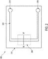
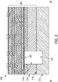
- Figs. 2 and 3 show two schematic views of another embodiment of a photonic sensor chip 200 that includes a microfluidic substrate 210.
- the photonic sensor chip 200 of the present embodiment comprises a photonic sensor core 220, which in the present example is a photonic sensor chip 100 as shown and explained in the context of the description of Fig. 1 .
- a microfluidic substrate 210 is attached to the photonic sensor core 220 on the back side 216 of its semiconductor substrate 212.
- the microfluidic substrate 210 comprises a microfluidic channel 230, which in the present example connects an inlet 240 for a fluid and an outlet 250 for the fluid with the cavity 218. Since the back of the photonic sensor core 220 is formed by a planar silicon surface, the integration of microfluidics is considerably simplified compared to frontal integration.
- connection of the microfluidic substrate 210 to the semiconductor substrate 212 can be realized by wafer bonding for many of the materials mentioned.
- the ability to use a wafer bonding technique thus forms an additional advantage of the of the structure of the photonic sensor chip 200 which substantially simplifies the fabrication process.
- microfluidic system 210 on the back side 216 of the semiconductor substrate 212 allows at least one fluid or gas to contact the active surface of the active-surface element 222 for allowing a detection of particles contained in the fluid or gas. Further, the use of microfluidics can increase the sensitivity of the measurement.
- a biosensor resulting from this design can implement a laboratory diagnostic procedure integrated on a chip (lab-on-a-chip) and, in contrast to conventional on-site diagnostic procedures, is characterized by its miniaturization, sensitivity, parallelization and diversification possibilities.
- the advantage of the photonic measurement method proposed here over other label-free technologies that have already been developed is, on the one hand, the high inherent sensitivity of the measurement principle, the independence of the measurement signal from the amount of bound water and the possibility of producing cost-effective disposable chips.
- This approach combines the advantages of optical sensor technology (as with SPR) with the possibilities of chip production (as with SAW). In this way, components are provided that are suitable for practical use in bioanalytics.
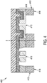
- FIG. 4 shows a schematic cross-sectional view of different embodiments having different waveguide types 400, as used in embodiments of the photonic sensor chip.
- Two different types of slot waveguides 410 are presented in Fig. 4 . Both types of the slot waveguide 410 are fabricated from the back side 416 of the semiconductor substrate 412 of a photonic sensor chip. Both slot waveguide 400s are located on an island-like silicon-on-insulator (SOI) structure 414.
- SOI silicon-on-insulator
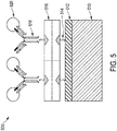
- Fig. 5 shows a functionalized silicon waveguide section 500 for specific application using a photonic sensor chip.
- the waveguide 510 in this embodiment is made of silicon. Silicon can be functionalized with organosilanes, which have an organic group at one end.
- amino-propyl-triethoxisilane (APTES) 512 is used to chemically react in a silanization with the silicon waveguide 510.
- APTES has an amino-group at the end, which is not bonded to the silicon waveguide 510.
- the amino-group is covalently bonding biotin 514.
- Streptavidin molecules which have a high affinity for biotin 514, are bonding to the biotin 514. Thus, a streptavidin 516 layer is formed.
- the streptavidin layer 516 can bind a biotinylated anti-CRP-complex 518, such that the waveguide section 500 has a functionalized surface section, which is suitable for specific detection of CRP molecules 520.
- a biotinylated anti-CRP-complex 518 such that the waveguide section 500 has a functionalized surface section, which is suitable for specific detection of CRP molecules 520.
- other anti-complexes can be bonded.
- biosensor designs are photonic devices that allow the conversion of a refractive index change into an evaluable signal.
- transducer components are Mach-Zehnder interferometers, ring resonators and Fabry-Perot resonators.
- Fig. 6 shows illustrations of two different optical ring resonators 600 for use in a photonic sensor chip. Both ring resonator geometries form hybrid waveguide ring resonators.
- the ring resonators comprise a channel waveguide 610, such as in the upper example, or a slot waveguide 620, cf. the lower example.
- the detection limit for ring resonators is currently 10 -5 RIU (refractive index unit).
- the waveguide section 650 of the active-surface element is functionalized with specific ligands, as described above.
- Chip-integrated photonic sensors such as optical ring resonators 600 can contribute to major advances in food diagnostics, environmental monitoring, veterinary diagnostics and medical technology through rapid and accurate analysis of a wide range of substances and offer the prospect of cost-effective on-site analysis.
- Fig. 7 shows a diagram of functionalized surface sections of different waveguides 700 capturing particles using in a photonic sensor chip.
- the upper left diagram shows a channel waveguide 710 arranged on the active-surface element, which has a functionalized surface section 716 functionalized with specific ligands 712.
- the functionalized surface 716 section is exposed to a fluid or gas without selected particles to be captured.
- the upper right diagram shows the mentioned channel waveguide 710 exposed to a fluid or gas with selected particles 714 to be captured.
- the selected particles 714 were captured by the specific ligands 712.
- the same principle works for a slot waveguide 720, which is shown in the lower row.
- Fig. 8 shows transmission spectrum 800 of measurement of the situations shown in Fig. 7 with a photonic sensor chip.
- ⁇ (shown as red line in Fig. 8 ) resulting in a resulting optical output wave 820 from the active-surface element to a light detector, which is shifted by ⁇ .
- the magnitude of the wavelength shift provides information about the amount of captured specific particles and thus about its concentration in the solution to be analysed.
- the optical input wave is guided in the silicon waveguide and interacts only through an evanescent field with the captured specific particles.
- silicon slit waveguides ensure a significantly increased interaction between the guided optical input wave and the captured specific particle, as a large part of the optical input wave up to 75 % is guided in the slit and in the vicinity of the silicon webs where the captured specific particle is located.
- slot waveguides show a 3.5-fold greater light-particle interaction compared to channel waveguides.
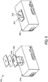
- Fig. 9 shows an embodiment of a photonic sensor arrangement 900.
- the photonic sensor arrangement comprises a packaged photonic sensor device 910 and a light source for generating the optical input wave, and an optical coupling element 914 for coupling the optical input wave into the photonic plane of the photonic sensor chip 916.
- the packaged photonic sensor device can generally be packaged using state of the art solutions, and includes a hole for providing access to the active-surface element of the particle sensor element of the photonic sensor chip a usage of the inventive photonic sensor chip cost-effective.
- the packaged photonic sensor device can be used as disposable product.
- the light source and the optical element are arranged inside a housing 918.
- the optical input wave is coupled into the photonic plane of the photonic sensor chip, for instance, by an optical fiber.
- the housing 918 also includes a data transmission unit configured to receive the output signal from the data acquisition unit and to transmit the output signal to an external device an interface unit configured to receive the output signal from the data acquisition unit and to indicate an amount of particles captured by the active surface.
- a data transmission unit configured to receive the output signal from the data acquisition unit and to transmit the output signal to an external device
- an interface unit configured to receive the output signal from the data acquisition unit and to indicate an amount of particles captured by the active surface.
- the photonic biosensor allows the selective and label-free detection of proteins or substances in general for which a specific capture molecule exists. Such evidence is relevant in many areas. Examples are the detection of proteins in food, toxins in the environment as well as the detection of substances in various body fluids in medical diagnostics or therapy monitoring.
- the sensor can also be used as a sensor without functionalizing the silicon surface. For example, it can be used as a gas sensor in which a change in refractive index is measured. An application for temperature measurement is also conceivable.
- Fig. 10 shows a schematic cross-sectional view of an embodiment of a photonic sensor chip 1000.
- the photonic sensor chip 1000 has a semiconductor substrate 1012 having a front side 1014 and a back side 1016.
- the photonic sensor chip 1000 includes a cavity 1018 extending from the back side 1016 through an entire depth of the semiconductor substrate 1012, which is for example a silicon substrate.
- the cavity 1018 provides access to the active surface of the photonic particle sensor element 1020 from the back side 1016 of the semiconductor substrate 1012.
- a photonic particle sensor element 1020 is arranged on the front side 1014 of the semiconductor substrate 1012 in a photonic plane 1024.
- the photonic particle sensor element 1020 comprises an active-surface element 1022 for capturing particles that is exposed for access from the back side 1016 of the semiconductor substrate 1012.
- the active-surface element 1022 comprises a waveguide section 1034 of a waveguide.
- An optical input wave is coupled into the photonic plane 1024 using a grating coupler 1026 arranged in the photonic plane 1024.
- the waveguide serves for guiding the optical input wave to the active-surface element, and further for guiding a resulting optical output wave to a light detector 1028, which in the present embodiment is a Ge-photodiode and is also arranged in the photonic plane 1024.
- FEOL front-end-of-line
- BEOL back-end-of-line
- the FEOL fabrication involves manufacturing NMOS devices, PMOS devices and SiGe:C HBTs.
- the FEOL fabrication also involves manufacturing of the Ge-photodiode.
- the electronic components can for instance form a circuit section or a complete circuit of a control unit, a data acquisition unit or other electrical circuitry.
- the photonic sensor chip 1000 is thus a SiGe BiCMOS device 1036.
- a thermal heating element 1032 is arranged in a metal layer of an interconnect stack 1035 located above the functionalized surface section of the active-surface element. Locating the thermal heating element 1032 above the functionalized surface section of the active-surface element allows calibrating the resonance condition of the photonic particle sensor element 1020 and stabilizing the temperature during measurements at the same time. For calibration the optical resonance of the photonic particle sensor element is shifted such that, the optical input wave received by the photonic particle sensor element lies on the resonance flank or the resonance peak. Stabilization of the temperature during the measurement is essential due to very specific binding affinities of biomolecules, which shall be captured by the photonic particle sensor element 1020.
- the electrical interconnect stack 1035 comprises electrical interconnects 1038 for conducting electrical operating power to the mentioned electro-optical and electronic components and to conduct electronic signals to and from the electro-optical and electronic components to their respective destinations on chip or to an interface to external circuits.
- the waveguide in the photonic plane 1024 is arranged on a local island-like silicon-on-insulator (SOI) structure 1040 that is embedded in the bulk of the silicon substrate 1012.
- SOI silicon-on-insulator
- the SiGe BiCMOS 1036 is located next to the local island SOI 1040 on the bulk of silicon substrate 1012.
- Fig. 11a shows a block diagram an embodiment of a packaged photonic sensor device 1100A.
- the packaged photonic sensor device 1100A comprises a photonic sensor chip 1110A and an electronic control chip arranged on a carrier 1114.
- the electronic control chip electrically connected to the photonic sensor chip 1110A.
- the photonic sensor chip 1110A of the present embodiment is a photonic sensor chip 1110A as shown and explained in the context of the description of Fig. 1 .
- the electronic control chip comprises a control unit 1112, which is configured to drive operation of the at least one photonic particle sensor element on the photonic sensor chip, and a data acquisition unit 1116, which is configured to sample an output signal of the light detector. Further, a data transmission unit 1118 configured to receive the output signal from the data acquisition unit and an interface unit 1120 configured to receive the output signal from the data acquisition unit 1116 and to indicate an amount of particles captured by the active surface are arranged in the electronic control chip.
- Fig. 11b shows a block diagram another embodiment of a packaged photonic sensor device 1100B.
- a photonic sensor chip 1110B and an electronic control chip 1111 are separately provided in separate chips, which may be individually packaged or provided in a system-on-chip and provided together in one package.
- Fig. 11a For further details regarding the functionality of the photonic sensor chip 1110B and of the electronic control chip 1111 of this embodiment, reference is made to the description of Fig. 11a .
- Figs. 12 to 14 show different possibilities to arrange a plurality of active-surface elements in the photonic sensor chip.
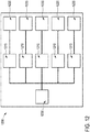
- Fig. 12 shows a possibility to arrange five active-surface elements in parallel 1200.
- Each active-surface element 1210 is arranged upstream of a photodiode 1220, which is used as light detector.
- One laser 1230 is used as light source for all active-surface elements 1210.
- An optical input wave transmitted by the laser can be splited to respective active-surface elements 1210.
- Such a parallel arrangement enables the detection of different selected particles in parallel.
- the signal-to-noise ratio of an optical output wave to be transformed into a corresponding electrical signal received by the light detector can be increased by using a series connection of active-surface elements.
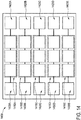
- Fig. 13 shows a possible arrangement to derive benefit of a parallel arrangement 1300 of the active-surface elements 1310 and a series connection of active-surface elements 1315.
- three active-surface elements in series connection are arranged upstream of respective photodiodes 1320.
- the arrangement of laser 1330 and photodiodes 1320 remains the same as in Fig. 12 .
- Fig. 14 displays an exemplarily arrangement 1400, where five lasers 1430A to 1430E and five photodiodes 1420A to 1420E are arranged in parallel. In between, three identical active-surface elements 1415A to 1415E are optically arranged in a series connection. Such arrangement of active-surface elements 1415A to 1415E allows to increase the signal-to-noise ratio of the resulting optical output wave to be transformed into a corresponding electrical signal by the photodiode due to the series connection. This arrangement 1400 also enables to detect of different selected particles in parallel due to the parallel connection.
- allergens in food such as peanuts
- toxins e.g. snake venom, toxic insects, scorpions, spiders, blue-green algae, mould poisons or poisonous fungi
- Table 1 Further applications of the photonic sensor chip are listed Table 1 below and can be followed or applied on the basis of the results obtained.
- the left column of the following table lists different analytes, and the right column list possible occurrences of the respective analytes.
- a cow is milked at least twice a day.
- the fresh raw milk is automatically piped into the cooling tank of the production plant.
- the raw milk is collected every one to two days from the producer in the milk collection truck. Depending on the vehicle type, this can hold between 10,000 and 25,000 litres.
- the smell, colour and temperature of the raw milk have been checked, it is pumped from the cooling tank into the milk collection truck.
- Milk samples are automatically taken and analysed in an independent laboratory or in the dairy. Once it arrives at the dairy, the raw milk is subjected to microbiological and chemical-physical checks for cleanliness, smell, taste, appearance, purity, fat content, acidity, germ content and weight. The milk is then pumped into large storage tanks.
- the solution proposed here considerably simplifies the development of a connection technique and the handling of the sensor, since the sensor surface is separated from the electronics and the light injection. This allows an analyte to interact with the sensor from the rear and does not interfere with further chip build-up. It is thus possible to manufacture the chip from the front with all the usual process steps, which also allows monolithic integration of the sensor.
- the photonic sensor is manufactured together with optoelectronic components (e.g. photodiodes) and electronic components (e.g. heating element).
- the bioanalytic part is accessible through the rear opening in the form of a cavity connecting to the optical sensor.
- a wafer, on which the photonic components are located is etched from the reverse side in such a way that the areas with the sensor surfaces are exposed and can be functionalized with antibodies.
- microfluidics on the back of the chip. Since the back of the chip consists of a planar silicon surface, the integration of microfluidics is considerably simplified compared to frontal integration.
Landscapes
- Chemical & Material Sciences (AREA)
- Health & Medical Sciences (AREA)
- Physics & Mathematics (AREA)
- Life Sciences & Earth Sciences (AREA)
- Immunology (AREA)
- General Physics & Mathematics (AREA)
- Engineering & Computer Science (AREA)
- Pathology (AREA)
- General Health & Medical Sciences (AREA)
- Analytical Chemistry (AREA)
- Biochemistry (AREA)
- Dispersion Chemistry (AREA)
- Molecular Biology (AREA)
- Food Science & Technology (AREA)
- Microelectronics & Electronic Packaging (AREA)
- Optics & Photonics (AREA)
- Chemical Kinetics & Catalysis (AREA)
- Plasma & Fusion (AREA)
- Biomedical Technology (AREA)
- Hematology (AREA)
- Urology & Nephrology (AREA)
- Medicinal Chemistry (AREA)
- Biophysics (AREA)
- Biotechnology (AREA)
- Cell Biology (AREA)
- Microbiology (AREA)
- Investigating Or Analysing Materials By Optical Means (AREA)
Abstract
Description
- The present invention relates to a photonic sensor chip, to a packaged photonic sensor device and to a photonic sensor arrangement.
- Photonic sensors have contributed to major advances in food diagnostics, environmental monitoring, veterinary diagnostics and medical technology through rapid and accurate analysis of a wide range of particles in a fluid or a gas. In fact, great progress has been made in recent years in photonic sensor technology for bioanalytics. Surface plasmon resonance (SPR) has become a standard technology applied for this purpose. However, as of today, this technology is quite expensive in terms of equipment and total costs regarding chips and service, and known sensors based on SPR are rather bulky.
- It would thus be desirable to achieve cheaper photonic sensor devices that are suitable for detecting particles in bioanalytics and offer the prospect of cost-effective on-site analysis.
- According to the first aspect of the invention, a photonic sensor chip according to
claim 1 is provided. The photonic sensor chip comprises: - a semiconductor substrate having a front side and a back side;
- at least one cavity extending from the back side through an entire depth of the semiconductor substrate;
- a photonic plane located on the front side of the semiconductor substrate and including
- at least one photonic particle sensor element with an active-surface element having an exposed active surface facing towards the back side of the semiconductor substrate and configured for capturing selected particles from at least one fluid or gas to which the active surface is exposable, wherein the least one cavity provides access to the active surface from the back side of the semiconductor substrate; and wherein
- the photonic particle sensor element is configured to receive an optical input wave via the photonic plane, to expose particles captured by the active-surface element to interact with the optical input wave and to provide a resulting optical output wave having a spectral component indicative of the interaction between the optical input wave and the captured particles.
- The photonic sensor chip includes at least one cavity extending from the back side through an entire depth of the semiconductor substrate. The cavity provides access to the active surface of the photonic particle sensor element from the back side of the semiconductor substrate. Thus, despite the arrangement of the photonic particle sensor element on the front side of the semiconductor substrate, it has an active-surface element for capturing particles that is exposed for access from the back side of the semiconductor substrate. Non-limiting examples of particles to be detected by the photonic particle sensor include, depending on a particular application purpose of a given embodiment, toxins, bacteria, viruses, allergens, antibiotics, hormones and other particles such as molecules.
- The photonic sensor chip allows, by means of its structure, fabricating the photonic particle sensor element independent from the constraints of device structure fabrication on the front side of the semiconductor substrate. In particular, the active surface of the active-surface element facing towards the back side of the semiconductor substrate and configured for capturing selected particles can be fabricated after fabrication of any front side structures. Also, fabrication steps required for forming the active-surface element can be performed separately from fabrication processes for manufacturing the photonic plane on the front side of the semiconductor substrate. This allows using materials in the fabrication of the active-surface element that are not compatible with standard front-end-of-line (FEOL) technology such as NMOS, PMOS, CMOS or BiCMOS, whereas the photonic plane on the front side of the semiconductor substrate can be fabricated using such highly developed and cost-efficient FEOL technology.
- Furthermore, the structure of the photonic sensor chip makes sure that, in operation, a fluid or gas which transports particles to be detected will not get in contact with the front side of the semiconductor substrate. Thus, potential exposure of the photonic sensor chip to a fluid or gas or to chemical reactions is restricted to the back side of the semiconductor substrate. This allows including integrated microelectronic components and complete electronic circuits on the front side of the photonic sensor chip, which will be described further below in more detail in the context of preferred embodiments. Therefore, the proposed photonic sensor chip is advantageously suited for integration in known semiconductor photonics concepts, including for instance complex device structures with integrated photonic, electro-optical, optoelectronic and electronic components on different levels.
- The photonic particle sensor element comprises a waveguide arranged in the photonic plane for guiding the optical input wave to the active-surface element and for guiding the resulting optical output wave from the active-surface element to a light detector of the photonic particle sensor element. Thus, improving the light guiding to the active-surface element is achieved. The waveguide guides the optical input wave in a defined manner to the active-surface element, and guides the resulting optical output wave to a light detector of the photonic particle sensor element.
- The photonic sensor chip further comprises an electrically drivable phase shifter element. The phase shifter element is configured to set and maintain a predetermined phase shift to be effected by the active-surface element alone, i.e., without influence by particles to be detected. With the phase shifter element, the photonic sensor chip is able to adapt the phase shift in order to improve the desired signal, i.e. desired information provided by the active-surface element with the optical output wave. As a result, a signal-to-noise ratio of the optical output wave can be increased to improve the detectability of interaction between the optical input wave and the particles captured by the active-surface element.
- In the following, embodiments of the photonic sensor chip will be described.
- In some embodiments, the photonic sensor chip further comprises a control unit. The control unit receives the output signal of the light detector and is configured to drive the operation of the photonic particle sensor element on the photonic sensor chip. In particular, the control unit is configured to drive operation of the phase shifter element in dependence on the received output signal, in orderto set and maintain a predetermined phase shift effected by the active-surface element alone. In such embodiments, the light detector receives a signal indicative of a phase shift with respect to a stabilized reference phase. Thus, a stabilized intensity is achieved, and an intensity change is reliably attributable to a useful signal.
- In preferred embodiments, the photonic particle sensor element includes a photonic resonator, or interferometer structure, preferably in integrated form within the photonic sensor chip. The photonic particle sensor element is configured to exhibit a change of a resonance condition of the photonic resonator or interferomenter structure, for instance in the form of a change of an optical resonance wavelength, in dependence on a type of particle captured. The light amount at the output of the photonic resonator or interferometer structure and detected by the light detector thus depends on the phase shift effected in presence of the captured particles and exhibits a resonance peak or resonance dip. The change of the resonance condition thus forms a "finger print" of a given type of captured particle. Thus, determining a change of the resonance condition before and after capturing of particles allows determining the type of captured particle.
- In one embodiment, the resonance condition of the photonic particle sensor element can be changed by the phase shifter element as a result of the operation of the control unit. A control of the resonance condition is achieved in that the optical resonance of the photonic particle sensor element can be shifted. Such resonance control allows using a cost-effective monochromatic light source. Further, fabrication tolerances can change the resonance conditions that can be compensated by the phase shifter.
- Suitably, to achieve sensitivity of the photonic resonator to a phase shift of any sign, the control unit is configured to control a shift of the optical resonance of the photonic particle sensor element such that the optical input wave received by the photonic particle sensor element lies on a resonance flank in absence of any captured particle. Captured particles thus cause either an increase or decrease of the light amount detected by the light detector, in dependence on a positive or negative phase shift effected by the particles. In another example, the resonance peak is used as the reference phase in absence of captured particles. In this alternative, captured particles always cause the same sign or direction of change of the light amount, irrespective of the sign of the phase shift effected by the captured particles.
- Suitable electrically drivable phase shifter elements are an electrically drivable heating element embedded in the electrical interconnect stack, or an electrically drivable doped waveguide. The heating element or the doped waveguide is suitably connected via the electrical interconnects. The heating element is preferably a resistance heater formed in the first metal layer of the interconnect stack in a lateral region coinciding or overlapping with that of the waveguide. The heating element changes the resonance condition of the photonic particle sensor element via the thermo-optical effect. In preferred embodiments, the control unit receives a feedback signal from the light detector. This is particularly useful in embodiments providing resonance control. Here, the feedback signal can be used in a tuning process for tuning the phase shift effected by the phase shifter element in controlling the resonance condition of the optical resonance of the photonic particle sensor element to a desired spectral position.
- In the latter example, the waveguide is doped in pn- or pin-diode configuration. The doped waveguide shifts the resonant condition of the photonic particle sensor element via changes in charge carrier density.
- In a further embodiment, the phase shifter element comprises both, a heating element and a doped waveguide.
- In an alternative embodiment, the heating element is used, beside resonance calibration, for optimum adjustment of temperature during the measuring process, in particular where a binding affinity of biomolecules is temperature dependent.
- In a preferred embodiment the photonic sensor chip further comprises a data acquisition unit configured to sample an output signal of the light detector. The photonic sensor chip of this embodiment is advantageous due to its compact design.
- In such embodiments, an electrical interconnect stack is preferably arranged on top of the photonic plane and comprises electrical interconnects for conducting electrical operating power and to conduct electronic signals to and from the control unit and the data acquisition unit. The electrical interconnect stack typically comprises the electrical interconnects on different metal planes which are separated from each other by a respective dielectric material layer and conductive vias, for conducting electrical operating power, and for conducting electronic signals to and from the control unit and the data acquisition unit.
- Such lab-on-a-chip design allows fabrication of particularly small and cost-effective solutions suitable for flexible application of the photonic sensor chip, e.g., in on-site diagnostics, for instance in dairy farming or mobile blood diagnostic equipment.
- As indicated before, the inventive photonic sensor chip increases the flexibility of usage. In further preferred embodiments of the photonic sensor chip, a microfluidic substrate is connected to the back side of the semiconductor substrate and comprises at least one microfluidic channel connecting an inlet for the fluid and an outlet for the fluid with the cavity. Regarding fabrication complexity, the connection of the microfluidic substrate on the back side of the semiconductor substrate according to the present embodiment is simpler in comparison to providing the microfluidics on the front side of the semiconductor substrate for access to the photonic particle sensor element.
- In different embodiments of the photonic sensor chip of this kind, the microfluidic substrate is made of a plastic, glass, quartz or a semiconductor, enabling an application-specific material selection for the microfluidic substrate. The connection of the microfluidic substrate to the semiconductor substrate can be realized by wafer bonding for many of the materials mentioned. Wafer bonding is a well-known and reliable technique. The ability to use a wafer bonding technique thus forms an additional advantage of the of the structure of the photonic sensor chip which substantially simplifies the fabrication process.
- Preferably, the semiconductor substrate is a silicon substrate, which for instance is formed from an industry-standard silicon wafer. In some embodiments of the photonic sensor chip of this kind, the waveguide in the photonic plane is arranged on a local island-like silicon-on-insulator (SOI) structure that is embedded in the bulk of the silicon substrate. This allows flexibly combining the advantages of using an SOI substrate for the photonic components and of using a silicon substrate surface for the microelectronic components and electrical connection lines.
- In preferred embodiments of the photonic sensor chip, the active-surface element comprises a waveguide section of the waveguide. The waveguide section comprises at least one functionalized surface section configured for capturing the selected particles by selective interaction, and has an optical path length that depends on an amount of particles captured by the active surface. The waveguide section, in some of these embodiments, has a ring resonator geometry. In alternative embodiments, the waveguide section is a ring assisted Mach-Zehnder interferometer or a Fabry-Perot resonator with photonic crystals. All of these waveguide sections have the similarity that they provide an optical signal conveying the information on detected particles in a manner that is suitable for converting into an electrical signal by the light detector.
- In other embodiments of the photonic sensor chip, the photonic particle sensor element comprises a plurality of active-surface elements optically arranged in a series connection and upstream of the light detector. Such arrangement of active-surface elements optically arranged in a series connection allows to increase the signal-to-noise ratio of the resulting optical output wave to be transformed into a corresponding electrical signal by the light detector.
- Different waveguide types can be used in the photonic sensor chip. In different exemplary embodiments, the waveguide is a strip waveguide, a slot waveguide, a rib waveguide or a strip-loaded slot waveguide on top of an insulating material layer.
- In another embodiment, the photonic sensor chip comprises a plurality of photonic particle sensor element arranged in parallel. Thus, a plurality of active-surface elements (or respective series of identical active-surface elements) are provided upstream of a corresponding plurality of light detectors. Such a parallel arrangements of photonic particle sensor elements enables the detection of different selected particles in parallel.
- Regarding the functionalized surface section of the waveguide section, different functionalization methods are possible. In some embodiments of the photonic sensor chip, the functionalized surface section is functionalized chemically. In exemplary embodiments of this kind, specific antibodies or ligands are covalently bonded to the surface of the waveguide section that forms the active surface element, resulting in a functionalized surface section. In other embodiments of the photonic sensor chip, the functionalized surface section is functionalized physically. For instance, the surface of the waveguide section forming the active-surface element has a roughness suitable for capturing particles. The roughness can be established in the fabrication process by physical treatment of the active-surface element, e.g., by ion bombardment.
- In other embodiments, a highly reflective metal, e.g. gold, is arranged between the functionalized surface section of the active-surface element and the waveguide section as an intermediate layer. This layer stack is suitable for application in a surface plasmon resonance spectroscopy technique. It is a further advantage of the photonic sensor chip of the present invention that such intermediate layer of gold can be deployed, even if industry standard fabrication processes are used for front side fabrication. Gold is a material that must not be used in standard FEOL processing.
- In different embodiments of the photonic sensor chip, the waveguide is substantially made of silicon, silicon nitride, silicon oxynitride or germanium. In the case of using silicon for the waveguide, either crystalline silicon, polysilicon or amorphous silicon can be used, depending on the requirements of the given application case.
- In a preferred embodiment, the photonic sensor chip comprises at least one light source, e.g., a vertical-cavity surface-emitting laser source or a light-emitting diode, connected to the waveguide and configured to generate and emit the optical input wave. The light source is arranged in the photonic plane. Alternatively, the light source is arranged in the interconnect stack or on top of the interconnect stack. In some variants of this embodiment, the light source is attached to the photonic sensor chip by a bonding technique, for example, via die-to wafer or wafer-to-wafer bonding.
- According to a second aspect of the invention, a packaged photonic sensor device is provided. The packaged photonic sensor device comprises:
- a photonic sensor chip according to an embodiment of the first aspect of the invention, wherein the photonic particle sensor element comprises a waveguide arranged in the photonic plane for guiding the optical input wave to the active-surface element and for guiding the resulting optical output wave from the active-surface element to a light detector of the photonic particle sensor element
- an electronic control chip electrically connected to the photonic sensor chip arranged on the carrier and comprising a control unit, which is configured to drive operation of the at least one photonic particle sensor element on the photonic sensor chip and a data acquisition unit configured to sample an output signal of the light detector;
- a package enclosing the photonic sensor chip and the electronic control chip and having an opening to ambient atmosphere facing the back side of the semiconductor substrate of the photonic sensor chip for providing access to the exposed active surface of the at least one photonic particle sensor element for the at least one fluid.
- The photonic sensor chip can be arranged on a carrier and packaged by state of the art solutions, including a hole for providing access to the active-surface element of the particle sensor element of the photonic sensor chip.
- According to a third aspect of the invention, a photonic sensor arrangement is provided. The photonic sensor arrangement comprises:
- a packaged photonic sensor device according to the second aspect of the invention or one of its embodiments, and
- a light source for generating the optical input wave, and an optical coupling element for coupling the optical input wave into the photonic plane of the photonic sensor chip.
- The optical input wave is coupled into the photonic plane of the photonic sensor chip, for instance, by an optical fiber. Alternatively, the optical input wave is coupled into the photonic plane of the photonic sensor chip by a free-steel optic using a suitable lens. The package of the photonic sensor device must take the respective coupling of light into account.
- In preferred embodiments the photonic sensor arrangement further comprises on the printed circuit board
- a data transmission unit configured to receive the output signal from the data acquisition unit and to transmit the output signal to an external device; and
- an interface unit configured to receive the output signal from the data acquisition unit and to indicate an amount of particles captured by the active surface.
- This embodiment allows an immediate verification of the analysed particles. For example, a cross-check of allergens or germ content in food. Thus, such photonic sensor arrangement is used for quality assurance in food industry. Alternatively, such photonic sensor arrangement is used in medicine diagnostic, e.g. for analysing blood composition. Also, in some embodiments the presence of toxins in ambient atmosphere can be detected.
- In the following, further embodiments will be described with reference to the enclosed drawings. In the drawings:
-
Fig. 1 shows a schematic cross-sectional view of an embodiment of a photonic sensor chip; -
Fig. 2 shows a schematic backside view of a photonic sensor chip that includes a microfluidic substrate; -
Fig. 3 shows a schematic cross-sectional view of the photonic sensor chip ofFig. 2 along a line III-III' shown inFig. 2 ; -
Fig. 4 shows a schematic cross-sectional view of different embodiments having different waveguide types, as used in embodiments of the photonic sensor chip; -
Fig. 5 shows a functionalized silicon waveguide section for specific application using a photonic sensor chip; -
Fig. 6 shows illustrations of two different optical ring resonators for use in a photonic sensor chip; -
Fig. 7 shows a diagram of functionalized surface sections of different waveguides capturing particles using in a photonic sensor chip; -
Fig. 8 shows transmission spectrum of measurement of the situations shown inFig. 7 with a photonic sensor chip; -
Fig. 9 shows an embodiment of a photonic sensor arrangement; -
Fig. 10 shows a schematic cross-sectional view of an embodiment of a photonic sensor chip; -
Fig. 11a shows a block diagram an embodiment of a packaged photonic sensor device. -
Fig. 11b shows a block diagram another embodiment of a packaged photonic sensor device. -
Fig. 12 to 14 show block diagrams of different embodiments of the photonic sensor chip; -
Fig. 1 shows a schematic cross-sectional view of an embodiment of aphotonic sensor chip 100. Thephotonic sensor chip 100 comprises asemiconductor substrate 112 having afront side 114 and aback side 116. Thephotonic sensor chip 100 includes acavity 118 extending from theback side 116 through an entire depth of thesemiconductor substrate 112, which is for example a silicon substrate. Thecavity 118 provides access to the active surface of the photonicparticle sensor element 120 from theback side 116 of thesemiconductor substrate 112. A photonicparticle sensor element 120 is arranged on thefront side 114 of the semiconductor substrate in aphotonic plane 124. The photonicparticle sensor element 120 comprises an active-surface element 122 for capturing particles that is exposed for access from theback side 116 of thesemiconductor substrate 100. In this embodiment the active-surface element 122 comprises awaveguide section 134 of a waveguide, which waveguide serves for guiding an optical input wave in a defined manner to the active-surface element 122, and further for guiding a resulting optical output wave to a light detector (not shown here), which is in this example a photodiode, of the photonic particle sensor element. Advantageously, the waveguide is embedded in oxide layers. - On the
front side 114 of thesemiconductor substrate 112 of thephotonic sensor chip 100, electro-optical andelectronic components 126 are arranged, and anelectrical interconnect stack 130 is provided on top of thephotonic plane 124. Theelectrical interconnect stack 130 compriseselectrical interconnects 132 for conducting electrical operating power to the electro-optical and electronic components, including the light detector, and to conduct electronic signals to and from the electro-optical and electronic components to their respective destinations on chip or to an interface to external circuits. The opto-electronic and electronic components are fabricated using known front-end-of-line (FEOL) such as NMOS, PMOS, CMOS or BiCMOS, or a photodiode as light detector and theinterconnect stack 132 can be fabricated using standard back-end-of-line (BEOL) technologies. Theelectronic components 126 can for instance form a circuit section or a complete circuit of a control unit, a data acquisition unit or other electrical circuitry. - The shown
photonic sensor chip 100 makes sure that, in operation, a fluid or gas which transports particles to be detected at the active-surface element 122 in thecavity 118 will not get in contact with thefront side 114 of thesemiconductor substrate 112. In this example, the measuring solution is applied directly to the sensor surface as a drop. Thus, potential exposure of thephotonic sensor chip 100 to a fluid or gas or to chemical reactions is restricted to theback side 116 of thesemiconductor substrate 112. - The combination of photonic components with state-of-the-art silicon-based microtechnology is forms key to development of a biosensors according to embodiments of the present invention.
- Thus, while prior art photonic devices are etched from the wafer surface and subsequently functionalized and electronic circuits located on the individual metal levels cannot be integrated, the innovative approach exemplified by the embodiment of
Fig. 1 uncovers the back of the photonic components. This approach enables for the first time an interaction between the analyte and the functionalized silicon waveguide and the simultaneous integration of electronic circuits on the chip top including the complete BEOL metallization layers. -
Figs. 2 and3 show two schematic views of another embodiment of aphotonic sensor chip 200 that includes amicrofluidic substrate 210. The following description will refer to both figures in parallel. Thephotonic sensor chip 200 of the present embodiment comprises aphotonic sensor core 220, which in the present example is aphotonic sensor chip 100 as shown and explained in the context of the description ofFig. 1 . Amicrofluidic substrate 210 is attached to thephotonic sensor core 220 on the back side 216 of its semiconductor substrate 212. Themicrofluidic substrate 210 comprises amicrofluidic channel 230, which in the present example connects aninlet 240 for a fluid and anoutlet 250 for the fluid with the cavity 218. Since the back of thephotonic sensor core 220 is formed by a planar silicon surface, the integration of microfluidics is considerably simplified compared to frontal integration. - The connection of the
microfluidic substrate 210 to the semiconductor substrate 212 can be realized by wafer bonding for many of the materials mentioned. The ability to use a wafer bonding technique thus forms an additional advantage of the of the structure of thephotonic sensor chip 200 which substantially simplifies the fabrication process. - The integration of
microfluidic system 210 on the back side 216 of the semiconductor substrate 212 allows at least one fluid or gas to contact the active surface of the active-surface element 222 for allowing a detection of particles contained in the fluid or gas. Further, the use of microfluidics can increase the sensitivity of the measurement. - A biosensor resulting from this design can implement a laboratory diagnostic procedure integrated on a chip (lab-on-a-chip) and, in contrast to conventional on-site diagnostic procedures, is characterized by its miniaturization, sensitivity, parallelization and diversification possibilities. The advantage of the photonic measurement method proposed here over other label-free technologies that have already been developed is, on the one hand, the high inherent sensitivity of the measurement principle, the independence of the measurement signal from the amount of bound water and the possibility of producing cost-effective disposable chips. This approach combines the advantages of optical sensor technology (as with SPR) with the possibilities of chip production (as with SAW). In this way, components are provided that are suitable for practical use in bioanalytics.
- As mentioned different waveguide types can be used in different embodiments of a photonic sensor chip.
Fig. 4 shows a schematic cross-sectional view of different embodiments havingdifferent waveguide types 400, as used in embodiments of the photonic sensor chip. Two different types ofslot waveguides 410 are presented inFig. 4 . Both types of theslot waveguide 410 are fabricated from theback side 416 of thesemiconductor substrate 412 of a photonic sensor chip. Both slot waveguide 400s are located on an island-like silicon-on-insulator (SOI)structure 414. -
Fig. 5 shows a functionalizedsilicon waveguide section 500 for specific application using a photonic sensor chip. Thewaveguide 510 in this embodiment is made of silicon. Silicon can be functionalized with organosilanes, which have an organic group at one end. In this embodiment amino-propyl-triethoxisilane (APTES) 512 is used to chemically react in a silanization with thesilicon waveguide 510. APTES has an amino-group at the end, which is not bonded to thesilicon waveguide 510. The amino-group is covalently bondingbiotin 514. Streptavidin molecules, which have a high affinity forbiotin 514, are bonding to thebiotin 514. Thus, astreptavidin 516 layer is formed. Thestreptavidin layer 516 can bind a biotinylated anti-CRP-complex 518, such that thewaveguide section 500 has a functionalized surface section, which is suitable for specific detection ofCRP molecules 520. Depending on the specification of the photonic sensor chip, other anti-complexes can be bonded. - Examples of biosensor designs are photonic devices that allow the conversion of a refractive index change into an evaluable signal. Examples of such transducer components are Mach-Zehnder interferometers, ring resonators and Fabry-Perot resonators.
Fig. 6 shows illustrations of two differentoptical ring resonators 600 for use in a photonic sensor chip. Both ring resonator geometries form hybrid waveguide ring resonators. The ring resonators comprise achannel waveguide 610, such as in the upper example, or aslot waveguide 620, cf. the lower example. The detection limit for ring resonators is currently 10-5 RIU (refractive index unit). In order to realize a selective interaction of theoptical input wave 630 with the active-surface element 640, thewaveguide section 650 of the active-surface element is functionalized with specific ligands, as described above. Chip-integrated photonic sensors, such asoptical ring resonators 600 can contribute to major advances in food diagnostics, environmental monitoring, veterinary diagnostics and medical technology through rapid and accurate analysis of a wide range of substances and offer the prospect of cost-effective on-site analysis. -
Fig. 7 shows a diagram of functionalized surface sections ofdifferent waveguides 700 capturing particles using in a photonic sensor chip. The upper left diagram shows achannel waveguide 710 arranged on the active-surface element, which has a functionalizedsurface section 716 functionalized withspecific ligands 712. Thefunctionalized surface 716 section is exposed to a fluid or gas without selected particles to be captured. The upper right diagram shows the mentionedchannel waveguide 710 exposed to a fluid or gas with selectedparticles 714 to be captured. The selectedparticles 714 were captured by thespecific ligands 712. The same principle works for aslot waveguide 720, which is shown in the lower row. - Label-free detection of biomolecules is thus enabled by integrating a photonic resonator or interferometer structure into the chip along with other photonic and electronic components. In order to realize a selective interaction with the analyte, the silicon-based
waveguide Fig. 8 showstransmission spectrum 800 of measurement of the situations shown inFig. 7 with a photonic sensor chip. Theblack line 810 inFig. 8 represents a resulting optical output wave from the active-surface element to a light detector, which is not influenced by captured specific particles. When the specific particles captured by thespecific ligands 712 the optical input wave is influenced. The resonance condition changes and the resonance wavelength is shifted by Δλ (shown as red line inFig. 8 ) resulting in a resultingoptical output wave 820 from the active-surface element to a light detector, which is shifted by Δλ. The magnitude of the wavelength shift provides information about the amount of captured specific particles and thus about its concentration in the solution to be analysed. - With an ordinary silicon channel waveguide, the optical input wave is guided in the silicon waveguide and interacts only through an evanescent field with the captured specific particles. In comparison, silicon slit waveguides ensure a significantly increased interaction between the guided optical input wave and the captured specific particle, as a large part of the optical input wave up to 75 % is guided in the slit and in the vicinity of the silicon webs where the captured specific particle is located. Thus, slot waveguides show a 3.5-fold greater light-particle interaction compared to channel waveguides.
-
Fig. 9 shows an embodiment of aphotonic sensor arrangement 900. The photonic sensor arrangement comprises a packagedphotonic sensor device 910 and a light source for generating the optical input wave, and an optical coupling element 914 for coupling the optical input wave into the photonic plane of thephotonic sensor chip 916. The packaged photonic sensor device can generally be packaged using state of the art solutions, and includes a hole for providing access to the active-surface element of the particle sensor element of the photonic sensor chip a usage of the inventive photonic sensor chip cost-effective. The packaged photonic sensor device can be used as disposable product. In this embodiment, the light source and the optical element are arranged inside ahousing 918. The optical input wave is coupled into the photonic plane of the photonic sensor chip, for instance, by an optical fiber. Thehousing 918 also includes a data transmission unit configured to receive the output signal from the data acquisition unit and to transmit the output signal to an external device an interface unit configured to receive the output signal from the data acquisition unit and to indicate an amount of particles captured by the active surface. Suchphotonic sensor arrangement 900 has the advantage that it is portable, which is of particular importance for the practical implementation. - The photonic biosensor allows the selective and label-free detection of proteins or substances in general for which a specific capture molecule exists. Such evidence is relevant in many areas. Examples are the detection of proteins in food, toxins in the environment as well as the detection of substances in various body fluids in medical diagnostics or therapy monitoring. In addition, the sensor can also be used as a sensor without functionalizing the silicon surface. For example, it can be used as a gas sensor in which a change in refractive index is measured. An application for temperature measurement is also conceivable.
-
Fig. 10 shows a schematic cross-sectional view of an embodiment of aphotonic sensor chip 1000. Thephotonic sensor chip 1000 has asemiconductor substrate 1012 having afront side 1014 and a back side 1016. Thephotonic sensor chip 1000 includes acavity 1018 extending from the back side 1016 through an entire depth of thesemiconductor substrate 1012, which is for example a silicon substrate. Thecavity 1018 provides access to the active surface of the photonicparticle sensor element 1020 from the back side 1016 of thesemiconductor substrate 1012. A photonicparticle sensor element 1020 is arranged on thefront side 1014 of thesemiconductor substrate 1012 in aphotonic plane 1024. The photonicparticle sensor element 1020 comprises an active-surface element 1022 for capturing particles that is exposed for access from the back side 1016 of thesemiconductor substrate 1012. In this embodiment, the active-surface element 1022 comprises awaveguide section 1034 of a waveguide. An optical input wave is coupled into thephotonic plane 1024 using agrating coupler 1026 arranged in thephotonic plane 1024. The waveguide serves for guiding the optical input wave to the active-surface element, and further for guiding a resulting optical output wave to alight detector 1028, which in the present embodiment is a Ge-photodiode and is also arranged in thephotonic plane 1024. - On the
front side 1014 of thesemiconductor substrate 1012 of thephotonic sensor chip 1000,electronic components 1030 are arranged, which are fabricated using known front-end-of-line (FEOL) and the interconnect stack can be fabricated using standard back-end-of-line (BEOL) technologies. In this example, the FEOL fabrication involves manufacturing NMOS devices, PMOS devices and SiGe:C HBTs. The FEOL fabrication also involves manufacturing of the Ge-photodiode. The electronic components can for instance form a circuit section or a complete circuit of a control unit, a data acquisition unit or other electrical circuitry. Thephotonic sensor chip 1000 is thus aSiGe BiCMOS device 1036. Athermal heating element 1032 is arranged in a metal layer of aninterconnect stack 1035 located above the functionalized surface section of the active-surface element. Locating thethermal heating element 1032 above the functionalized surface section of the active-surface element allows calibrating the resonance condition of the photonicparticle sensor element 1020 and stabilizing the temperature during measurements at the same time. For calibration the optical resonance of the photonic particle sensor element is shifted such that, the optical input wave received by the photonic particle sensor element lies on the resonance flank or the resonance peak. Stabilization of the temperature during the measurement is essential due to very specific binding affinities of biomolecules, which shall be captured by the photonicparticle sensor element 1020. Theelectrical interconnect stack 1035 comprises electrical interconnects 1038 for conducting electrical operating power to the mentioned electro-optical and electronic components and to conduct electronic signals to and from the electro-optical and electronic components to their respective destinations on chip or to an interface to external circuits. In this embodiment, the waveguide in thephotonic plane 1024 is arranged on a local island-like silicon-on-insulator (SOI)structure 1040 that is embedded in the bulk of thesilicon substrate 1012. TheSiGe BiCMOS 1036 is located next to thelocal island SOI 1040 on the bulk ofsilicon substrate 1012. -
Fig. 11a shows a block diagram an embodiment of a packagedphotonic sensor device 1100A. In this exemplary embodiment, the packagedphotonic sensor device 1100A comprises aphotonic sensor chip 1110A and an electronic control chip arranged on acarrier 1114. The electronic control chip electrically connected to thephotonic sensor chip 1110A. - The
photonic sensor chip 1110A of the present embodiment is aphotonic sensor chip 1110A as shown and explained in the context of the description ofFig. 1 . The electronic control chip comprises acontrol unit 1112, which is configured to drive operation of the at least one photonic particle sensor element on the photonic sensor chip, and adata acquisition unit 1116, which is configured to sample an output signal of the light detector. Further, adata transmission unit 1118 configured to receive the output signal from the data acquisition unit and aninterface unit 1120 configured to receive the output signal from thedata acquisition unit 1116 and to indicate an amount of particles captured by the active surface are arranged in the electronic control chip. - For packaging, state of the art solutions can be used, including fabrication of a hole for providing access to the active-surface element of the particle sensor element of the
photonic sensor chip 1110A. -
Fig. 11b shows a block diagram another embodiment of a packagedphotonic sensor device 1100B. In this embodiment, aphotonic sensor chip 1110B and anelectronic control chip 1111 are separately provided in separate chips, which may be individually packaged or provided in a system-on-chip and provided together in one package. For further details regarding the functionality of thephotonic sensor chip 1110B and of theelectronic control chip 1111 of this embodiment, reference is made to the description ofFig. 11a . -
Figs. 12 to 14 show different possibilities to arrange a plurality of active-surface elements in the photonic sensor chip. -
Fig. 12 shows a possibility to arrange five active-surface elements in parallel 1200. Each active-surface element 1210 is arranged upstream of aphotodiode 1220, which is used as light detector. Onelaser 1230 is used as light source for all active-surface elements 1210. An optical input wave transmitted by the laser can be splited to respective active-surface elements 1210. Such a parallel arrangement enables the detection of different selected particles in parallel. - The signal-to-noise ratio of an optical output wave to be transformed into a corresponding electrical signal received by the light detector, can be increased by using a series connection of active-surface elements.
Fig. 13 shows a possible arrangement to derive benefit of a parallel arrangement 1300 of the active-surface elements 1310 and a series connection of active-surface elements 1315. In contrast to the arrangement inFig. 12 three active-surface elements in series connection are arranged upstream of respective photodiodes 1320. The arrangement of laser 1330 and photodiodes 1320 remains the same as inFig. 12 . -
Fig. 14 displays an exemplarily arrangement 1400, where five lasers 1430A to 1430E and five photodiodes 1420A to 1420E are arranged in parallel. In between, three identical active-surface elements 1415A to 1415E are optically arranged in a series connection. Such arrangement of active-surface elements 1415A to 1415E allows to increase the signal-to-noise ratio of the resulting optical output wave to be transformed into a corresponding electrical signal by the photodiode due to the series connection. This arrangement 1400 also enables to detect of different selected particles in parallel due to the parallel connection. - As an application example of the photonic sensor chip, allergens in food (such as peanuts) or toxins (e.g. snake venom, toxic insects, scorpions, spiders, blue-green algae, mould poisons or poisonous fungi) can be investigated. Further applications of the photonic sensor chip are listed Table 1 below and can be followed or applied on the basis of the results obtained. The left column of the following table lists different analytes, and the right column list possible occurrences of the respective analytes.
Table 1- Application cases of the photonic sensor chip analyte Occurrence toxins nuts, corn, milk aflatoxins ergot alkaloids cereals fusarium toxins cereals, maize patulin Apples, pears ochratoxin Cereals, beer, wine, coffee, nuts, spices bacteria eggs, poultry, water Salmonella (zoonoses) Escherichia coli raw milk, vegetables, water, minced beef, sprouts campylobacter Raw poultry meat shigella toxin food viruses birds, pig Influenza A virus H1N1 allergens food gluten antibiotics Waste water Meat Milk penicillins hormones Water - An important application potential is currently seen in the detection of contaminations such as antibiotics in raw milk.
- A cow is milked at least twice a day. The fresh raw milk is automatically piped into the cooling tank of the production plant. In principle, the raw milk is collected every one to two days from the producer in the milk collection truck. Depending on the vehicle type, this can hold between 10,000 and 25,000 litres. Once the smell, colour and temperature of the raw milk have been checked, it is pumped from the cooling tank into the milk collection truck. Milk samples are automatically taken and analysed in an independent laboratory or in the dairy. Once it arrives at the dairy, the raw milk is subjected to microbiological and chemical-physical checks for cleanliness, smell, taste, appearance, purity, fat content, acidity, germ content and weight. The milk is then pumped into large storage tanks. Seamless quality assurance from the producer to the refrigerated shelf is a matter of course for the German dairy industry. In order to further improve product safety, many dairies are developing additional quality assurance systems that go beyond the legal requirements. The close cooperation of all stakeholders within the value chain is crucial to ensure the production of safe and high quality products. The developed hybrid waveguide ring resonator can make a major contribution to this. In addition to fast on-site analysis, the sensor also enables digital evaluation and creation of databases without intermediate steps.
- In summary, the solution proposed here considerably simplifies the development of a connection technique and the handling of the sensor, since the sensor surface is separated from the electronics and the light injection. This allows an analyte to interact with the sensor from the rear and does not interfere with further chip build-up. It is thus possible to manufacture the chip from the front with all the usual process steps, which also allows monolithic integration of the sensor. In monolithic integration, the photonic sensor is manufactured together with optoelectronic components (e.g. photodiodes) and electronic components (e.g. heating element). The bioanalytic part is accessible through the rear opening in the form of a cavity connecting to the optical sensor. For this purpose, a wafer, on which the photonic components are located, is etched from the reverse side in such a way that the areas with the sensor surfaces are exposed and can be functionalized with antibodies.
- This also allows the integration of microfluidics on the back of the chip. Since the back of the chip consists of a planar silicon surface, the integration of microfluidics is considerably simplified compared to frontal integration.
- The solution proposed has the following advantages:
- Decentralized diagnostics without laboratory diagnostic prior knowledge
- A mobile sensor platform enables fast on-site diagnostics
- Measurement of several biological substances and parameters in parallel and in short time can be enabled
- Functionalized surfaces with customized properties for bioanalytics
- The optical biosensor can be used for almost any requirements in medicine and industry due to its adaptable and functional optical waveguides
- Compatibility of photonic with electronic components on one chip without additional process steps (integration with separation of electrical and biosensory environment)
- Low-cost in terms of manufacturing and disposal costs (due to the CMOS technology used and the avoidance of complex and very expensive flow cells)
- Suitable for mass production, as the manufacturing and process technology is designed at wafer level
- Low power requirements and extremely high compactness (this offers the possibility of sensor arrays on a small area and the realization of mobile, battery-powered devices)
Claims (15)
- A photonic sensor chip (100, 200, 1000) comprising- a semiconductor substrate (112, 212, 1012) having a front side (114, 214, 1014) and a back side (116, 216, 1016);- at least one cavity (118, 218, 1018) extending from the back (116, 216, 1016) side through an entire depth of the semiconductor substrate (112, 212, 1012);- a photonic plane (124, 1024) located on the front side (114, 214, 1014) of the semiconductor substrate (112, 212, 1012) and including- at least one photonic particle sensor element (120, 1020) with an active-surface element (122, 222, 1022) having an exposed active surface facing towards the back side (116, 216, 1016) of the semiconductor substrate (112, 212, 1012) and configured for capturing selected particles from at least one fluid or gas to which the active surface is exposable, wherein the least one cavity (118, 218, 1018) provides access to the active surface from the back side (116, 216, 1016) of the semiconductor substrate (112, 212, 1012); and wherein- the photonic particle sensor element (120, 1020) is configured to receive an optical input wave via the photonic plane (124, 1024), to expose particles captured by the active-surface element (122, 222, 1022) to interact with the optical input wave and to provide a resulting optical output wave having a spectral component indicative of the interaction between the optical input wave and the captured particles; and- a waveguide arranged in the photonic plane (1024) for guiding the optical input wave to the active-surface element (1022) and for guiding the resulting optical output wave from the active-surface element (1022) to a light detector (1028) of the photonic particle sensor element (1020), which is configured to generate an output signal in response to receiving the optical output wave; the photonic sensor chip further comprising- an electrically drivable phase shifter element (1032), which is configured to set and maintain a predetermined phase shift to be effected by the active-surface element (1022) alone.
- A photonic sensor chip (100) according to claim 1, further comprising- a control unit (1112), which receives the output signal of the light detector (1028) and is configured to drive operation of the at least one photonic particle sensor element (1022); wherein- the control unit (1112) is configured to drive operation of the phase shifter element (1032) in dependence on the received output signal of the light detector in order to set and maintain a predetermined phase shift to be effected by the active-surface element (1022) alone.
- A photonic sensor chip (200) according to claim 1 or 2, wherein the electrically drivable phase shifter element comprises an electrically drivable heating element embedded in the electrical interconnect stack, or an electrically drivable doped waveguide.
- A photonic sensor chip (100) according to claim 2 or 3,- a data acquisition unit (1116) configured to sample an output signal of the light detector (1028); and- an electrical interconnect stack (1030), which is arranged on top of the photonic plane (1024) and comprises electrical interconnects (1038) for conducting electrical operating power and to conduct electronic signals to and from the control unit and the data acquisition unit (1116).
- A photonic sensor chip (200) according to any of the preceding claims, wherein a microfluidic substrate (210) is connected to the back side (216) of the semiconductor substrate (212) and comprises at least one microfluidic channel (230) connecting an inlet for the fluid and an outlet (250) for the fluid with the cavity (218).
- A photonic sensor chip (200) according to claim 5, wherein the microfluidic substrate (210) is made of a plastic, glass or semiconductor.
- A photonic sensor chip (100, 200, 1000) according to any of the preceding claims, wherein the active-surface element (122, 222, 1022) comprises a waveguide section (134, 650, 1034) of the waveguide (510, 610), wherein the waveguide section (134, 650, 1034)- comprises at least one functionalized surface section (500) configured for capturing the selected particles by selective interaction, and- has an optical path length that depends on an amount of particles captured by the active surface.
- A photonic sensor chip (100, 200, 1000) according to claim 7, wherein the photonic particle sensor element (120, 1020) comprises a plurality of active-surface elements (122, 222, 1022) optically arranged in a series connection and upstream of the light detector (1028).
- A photonic sensor chip (100, 200, 1000) according to any of the preceding claims, wherein the functionalized surface section (500) is functionalized chemically.
- A photonic sensor chip (100, 200, 1000) according to any of the preceding claims, wherein the functionalized surface section (500) is functionalized physically.
- A photonic sensor chip (100, 200, 1000) according to any of the preceding claims, wherein the waveguide is substantially made of silicon, silicon nitride, silicon oxynitride or germanium.
- A photonic sensor chip (100, 200, 1000) according at least one of the preceding claims, further comprising- at least one light source (1230, 1330, 1430) connected to the waveguide and configured to generate and emit the optical input wave.
- A packaged photonic sensor device (1100), comprising- a photonic sensor chip (100, 200, 1000) according to at least one of the preceding claims;- an electronic control chip (1111) electrically connected to the photonic sensor chip (100, 200, 1000) arranged on a carrier (1114) and comprising a control unit (1112), which is configured to drive operation of the at least one photonic particle sensor element on the photonic sensor chip (100, 200, 1000) and a data acquisition unit (1116) configured to sample an output signal of the light detector;- a package enclosing the photonic sensor chip (100, 200, 1000) and the electronic control chip (1111) and having an opening to ambient atmosphere facing the back side of the semiconductor substrate (112, 212, 1012) of the photonic sensor chip (100, 200, 1000) for providing access to the exposed active surface of the at least one photonic particle sensor element for the at least one fluid.
- A photonic sensor arrangement (900), comprising,- a packaged photonic sensor device (1100, 910) according to claim 13, and- a light source (1230, 1330, 1430) for generating the optical input wave, and an optical coupling element (914) for coupling the optical input wave into the photonic plane (124) of the photonic sensor chip (100).
- A photonic sensor arrangement (900) of claim 14, further comprising on the printed circuit board- a data transmission unit (1118) configured to receive the output signal from the data acquisition unit (1116) and to transmit the output signal to an external device; and- an interface unit (1120) configured to receive the output signal from the data acquisition unit (1116) and to indicate an amount of particles captured by the active surface.
Applications Claiming Priority (2)
| Application Number | Priority Date | Filing Date | Title |
|---|---|---|---|
| EP18215524 | 2018-12-21 | ||
| EP19166562.9A EP3671186A1 (en) | 2018-12-21 | 2019-04-01 | Photonic sensor chip, packaged photonic sensor device and arrangement |
Publications (3)
| Publication Number | Publication Date |
|---|---|
| EP3671187A1 true EP3671187A1 (en) | 2020-06-24 |
| EP3671187B1 EP3671187B1 (en) | 2025-03-19 |
| EP3671187C0 EP3671187C0 (en) | 2025-03-19 |
Family
ID=64959157
Family Applications (2)
| Application Number | Title | Priority Date | Filing Date |
|---|---|---|---|
| EP19166562.9A Withdrawn EP3671186A1 (en) | 2018-12-21 | 2019-04-01 | Photonic sensor chip, packaged photonic sensor device and arrangement |
| EP19218716.9A Active EP3671187B1 (en) | 2018-12-21 | 2019-12-20 | Photonic sensor chip, packaged photonic sensor device and arrangement |
Family Applications Before (1)
| Application Number | Title | Priority Date | Filing Date |
|---|---|---|---|
| EP19166562.9A Withdrawn EP3671186A1 (en) | 2018-12-21 | 2019-04-01 | Photonic sensor chip, packaged photonic sensor device and arrangement |
Country Status (2)
| Country | Link |
|---|---|
| US (1) | US11092742B2 (en) |
| EP (2) | EP3671186A1 (en) |
Cited By (3)
| Publication number | Priority date | Publication date | Assignee | Title |
|---|---|---|---|---|
| US20250149477A1 (en) * | 2023-11-03 | 2025-05-08 | Taiwan Semiconductor Manufacturing Company Limited | Photonic assembly for enhanced bonding yield and methods for forming the same |
| WO2025140845A1 (en) | 2023-12-28 | 2025-07-03 | Ihp Gmbh - Innovations For High Performance Microelectronics / Leibniz-Institut Für Innovative Mikroelektronik | Biosensor system and method for detecting a target analyte in a fluid sample |
| EP4588567A1 (en) | 2023-12-28 | 2025-07-23 | IHP GmbH - Innovations for High Performance Microelectronics / Leibniz-Institut für innovative Mikroelektronik | Biosensor system and method for detecting a target analyte in a fluid sample |
Families Citing this family (13)
| Publication number | Priority date | Publication date | Assignee | Title |
|---|---|---|---|---|
| WO2019226679A1 (en) | 2018-05-22 | 2019-11-28 | Fluxus, Inc. | Fabrication of waveguide structures |
| CN116472439A (en) * | 2020-11-04 | 2023-07-21 | 香港大学 | Optical soft-skin system for multimodal sensing |
| CN112838076A (en) * | 2021-01-04 | 2021-05-25 | 长江存储科技有限责任公司 | Package structure |
| EP4036639A1 (en) * | 2021-02-02 | 2022-08-03 | IHP GmbH - Innovations for High Performance Microelectronics / Leibniz-Institut für innovative Mikroelektronik | Method for producing an electro-optical phase shifter based on ferroelectric materials |
| US11500151B2 (en) * | 2021-02-22 | 2022-11-15 | Taiwan Semiconductor Manufacturing Company Limited | Semiconductor arrangement and method of making |
| CN116165176B (en) * | 2021-11-24 | 2025-12-09 | 上海驷格生物科技有限公司 | Chip-level biomolecule detection system and detection method |
| JP2025536233A (en) * | 2022-10-07 | 2025-11-05 | フルクサス,インク. | optofluidic devices |
| US12242107B2 (en) * | 2022-10-07 | 2025-03-04 | Fluxus, Inc. | Optofluidic devices |
| US20250083142A1 (en) * | 2023-09-08 | 2025-03-13 | Texas Instruments Incorporated | Multiplexed nucleic acid amplification test on semiconductor substrate |
| TWI899731B (en) * | 2023-12-04 | 2025-10-01 | 宏達國際電子股份有限公司 | Wearable device and communication method thereof |
| GR1010873B (en) | 2023-12-28 | 2025-02-06 | Αριστοτελειο Πανεπιστημιο Θεσσαλονικης-Ειδικος Λογαριαμος Κονδυλιων Ερευνας, | Optical interferometric sensing device in photonic integrated circuits |
| EP4579215B1 (en) * | 2023-12-28 | 2026-06-03 | IHP GmbH - Leibniz Institute for High Performance/ Leibniz Institute for Innovative Microelectronics | Chip-integrated luminescence detection for chemical, biological or biochemical sensing |
| WO2025140847A1 (en) * | 2023-12-28 | 2025-07-03 | Ihp Gmbh - Innovations For High Performance Microelectronics / Leibniz-Institut Für Innovative Mikroelektronik | Chip-integrated luminescence detection for chemical, biological or biochemical sensing |
Citations (7)
| Publication number | Priority date | Publication date | Assignee | Title |
|---|---|---|---|---|
| US20050035278A1 (en) * | 2003-08-13 | 2005-02-17 | Moti Margalit | Micro-resonator based optical sensor |
| EP1918693A1 (en) * | 2006-10-31 | 2008-05-07 | Honeywell International, Inc. | Optical waveguide sensor devices and methods for making and using them |
| US20090087137A1 (en) * | 2007-10-02 | 2009-04-02 | My The Doan | Planar lightwave circuits with air filled trenches |
| EP2515099A1 (en) * | 2011-04-21 | 2012-10-24 | Fraunhofer Gesellschaft zur Förderung der angewandten Wissenschaft E.V. | Method of detecting molecules and optical sensor |
| EP2581730A1 (en) * | 2011-10-10 | 2013-04-17 | Fraunhofer-Gesellschaft zur Förderung der angewandten Forschung | Optical Resonator for Sensor Arrangement and Measuring Method |
| US20180159293A1 (en) * | 2016-02-18 | 2018-06-07 | Oracle International Corporation | Ring-resonator-based laser with multiple wavelengths |
| WO2018150205A1 (en) * | 2017-02-17 | 2018-08-23 | Aristotle University Of Thessaloniki-Research Committee, E.L.K.E. | Integrated plasmo-photonic biosensor and method of use |
Family Cites Families (9)
| Publication number | Priority date | Publication date | Assignee | Title |
|---|---|---|---|---|
| US20100322824A1 (en) * | 2007-11-05 | 2010-12-23 | Koninklijke Philips Electronics N.V. | Biosensor cartridge |
| US9551650B2 (en) * | 2009-06-01 | 2017-01-24 | Cornell University | Integrated optofluidic system using microspheres |
| US9417186B2 (en) * | 2012-08-30 | 2016-08-16 | Infineon Technologies Ag | Opto-electronic sensor |
| KR102074945B1 (en) * | 2013-03-14 | 2020-02-07 | 삼성전자 주식회사 | Biophotonic sensor and bio sensing system |
| WO2015108589A2 (en) * | 2013-10-22 | 2015-07-23 | Massachusetts Institute Of Technology | Waveguide formation using cmos fabrication techniques |
| CN107209107A (en) * | 2015-04-30 | 2017-09-26 | 惠普发展公司有限责任合伙企业 | Microfluidic optical fluid sensor |
| DE102016103646B4 (en) * | 2016-01-22 | 2023-03-02 | Infineon Technologies Ag | INTEGRATED PHOTOACOUSTIC GAS SENSOR MODULE |
| US11073465B2 (en) * | 2017-08-21 | 2021-07-27 | The Board Of Trustees Of The University Of Illinois | Real-time sensing of flowing nanoparticles with electro-opto-mechanics |
| CN208520750U (en) * | 2018-07-27 | 2019-02-19 | 京东方科技集团股份有限公司 | A spectral detection device |
-
2019
- 2019-04-01 EP EP19166562.9A patent/EP3671186A1/en not_active Withdrawn
- 2019-12-18 US US16/718,595 patent/US11092742B2/en active Active
- 2019-12-20 EP EP19218716.9A patent/EP3671187B1/en active Active
Patent Citations (7)
| Publication number | Priority date | Publication date | Assignee | Title |
|---|---|---|---|---|
| US20050035278A1 (en) * | 2003-08-13 | 2005-02-17 | Moti Margalit | Micro-resonator based optical sensor |
| EP1918693A1 (en) * | 2006-10-31 | 2008-05-07 | Honeywell International, Inc. | Optical waveguide sensor devices and methods for making and using them |
| US20090087137A1 (en) * | 2007-10-02 | 2009-04-02 | My The Doan | Planar lightwave circuits with air filled trenches |
| EP2515099A1 (en) * | 2011-04-21 | 2012-10-24 | Fraunhofer Gesellschaft zur Förderung der angewandten Wissenschaft E.V. | Method of detecting molecules and optical sensor |
| EP2581730A1 (en) * | 2011-10-10 | 2013-04-17 | Fraunhofer-Gesellschaft zur Förderung der angewandten Forschung | Optical Resonator for Sensor Arrangement and Measuring Method |
| US20180159293A1 (en) * | 2016-02-18 | 2018-06-07 | Oracle International Corporation | Ring-resonator-based laser with multiple wavelengths |
| WO2018150205A1 (en) * | 2017-02-17 | 2018-08-23 | Aristotle University Of Thessaloniki-Research Committee, E.L.K.E. | Integrated plasmo-photonic biosensor and method of use |
Cited By (4)
| Publication number | Priority date | Publication date | Assignee | Title |
|---|---|---|---|---|
| US20250149477A1 (en) * | 2023-11-03 | 2025-05-08 | Taiwan Semiconductor Manufacturing Company Limited | Photonic assembly for enhanced bonding yield and methods for forming the same |
| US12554064B2 (en) * | 2023-11-03 | 2026-02-17 | Taiwan Semiconductor Manufacturing Company Limited | Photonic assembly for enhanced bonding yield and methods for forming the same |
| WO2025140845A1 (en) | 2023-12-28 | 2025-07-03 | Ihp Gmbh - Innovations For High Performance Microelectronics / Leibniz-Institut Für Innovative Mikroelektronik | Biosensor system and method for detecting a target analyte in a fluid sample |
| EP4588567A1 (en) | 2023-12-28 | 2025-07-23 | IHP GmbH - Innovations for High Performance Microelectronics / Leibniz-Institut für innovative Mikroelektronik | Biosensor system and method for detecting a target analyte in a fluid sample |
Also Published As
| Publication number | Publication date |
|---|---|
| EP3671187B1 (en) | 2025-03-19 |
| US20200200972A1 (en) | 2020-06-25 |
| US11092742B2 (en) | 2021-08-17 |
| EP3671186A1 (en) | 2020-06-24 |
| EP3671187C0 (en) | 2025-03-19 |
Similar Documents
| Publication | Publication Date | Title |
|---|---|---|
| EP3671187B1 (en) | Photonic sensor chip, packaged photonic sensor device and arrangement | |
| US5834777A (en) | NDIR gas sensor | |
| US8823947B2 (en) | Optical sensor and method for detecting molecules | |
| US7907282B2 (en) | Integrated sensing module for handheld spectral measurements | |
| CN107991479B (en) | Digital control of on-chip magnetic particle detection | |
| Minas et al. | A lab-on-a-chip for spectrophotometric analysis of biological fluids | |
| Tsai et al. | Real-time CRP detection from whole blood using micropost-embedded microfluidic chip incorporated with label-free biosensor | |
| JP5230149B2 (en) | Surface plasmon resonance sensor and biochip | |
| Lee et al. | A centrifugally actuated point-of-care testing system for the surface acoustic wave immunosensing of cardiac troponin I | |
| JP2013531222A (en) | Sample analysis system and method of use | |
| US10422895B2 (en) | Passive waveguide structures and integrated detection and/or imaging systems incorporating the same | |
| JP2015535087A (en) | System and method for integrated multiplexed photometric module | |
| US11366060B2 (en) | Apparatus for detecting fluorescent light emitted from a sample, a biosensor system, and a detector for detecting supercritical angle fluorescent light | |
| CN114631015A (en) | Test apparatus, assembly and method | |
| Gong et al. | Ammonia-trapping multilayer polymer urease film amplifier coated surface plasmon resonance sensor for ultra-sensitive urea detection | |
| Angelopoulou et al. | Multiplexed detection of food contaminants with a portable reader based on all-in-one monolithic photonic chips | |
| TWI815235B (en) | An optical absorbance spectrometer, optical device and method of optical absorbance spectrometry | |
| US9612197B2 (en) | Reflection-based tubular waveguide particle plasmon resonance sensing system and sensing device thereof | |
| WO2007064820A2 (en) | An integrated sensing system approach for handheld spectral measurements | |
| US12372522B2 (en) | Optical sensor, system and method for detecting pathogenic germs | |
| JP2006084210A (en) | Analysis equipment | |
| CN109975247A (en) | High-sensitivity biosensor and preparation method thereof | |
| CN117760989A (en) | Hemoglobin concentration calculation method, device and blood analyzer | |
| US20130329214A1 (en) | Application of spectral linewidth variation using optical filter | |
| EP4579215A1 (en) | Chip-integrated luminescence detection for chemical, biological or biochemical sensing |
Legal Events
| Date | Code | Title | Description |
|---|---|---|---|
| PUAI | Public reference made under article 153(3) epc to a published international application that has entered the european phase |
Free format text: ORIGINAL CODE: 0009012 |
|
| STAA | Information on the status of an ep patent application or granted ep patent |
Free format text: STATUS: THE APPLICATION HAS BEEN PUBLISHED |
|
| AK | Designated contracting states |
Kind code of ref document: A1 Designated state(s): AL AT BE BG CH CY CZ DE DK EE ES FI FR GB GR HR HU IE IS IT LI LT LU LV MC MK MT NL NO PL PT RO RS SE SI SK SM TR |
|
| AX | Request for extension of the european patent |
Extension state: BA ME |
|
| STAA | Information on the status of an ep patent application or granted ep patent |
Free format text: STATUS: REQUEST FOR EXAMINATION WAS MADE |
|
| 17P | Request for examination filed |
Effective date: 20210111 |
|
| RBV | Designated contracting states (corrected) |
Designated state(s): AL AT BE BG CH CY CZ DE DK EE ES FI FR GB GR HR HU IE IS IT LI LT LU LV MC MK MT NL NO PL PT RO RS SE SI SK SM TR |
|
| STAA | Information on the status of an ep patent application or granted ep patent |
Free format text: STATUS: EXAMINATION IS IN PROGRESS |
|
| 17Q | First examination report despatched |
Effective date: 20220811 |
|
| GRAP | Despatch of communication of intention to grant a patent |
Free format text: ORIGINAL CODE: EPIDOSNIGR1 |
|
| STAA | Information on the status of an ep patent application or granted ep patent |
Free format text: STATUS: GRANT OF PATENT IS INTENDED |
|
| RIC1 | Information provided on ipc code assigned before grant |
Ipc: G01N 15/1434 20240101ALN20240920BHEP Ipc: G01N 33/12 20060101ALN20240920BHEP Ipc: G01N 33/02 20060101ALN20240920BHEP Ipc: G01N 15/10 20060101ALN20240920BHEP Ipc: G01N 21/552 20140101ALN20240920BHEP Ipc: G01N 21/25 20060101ALN20240920BHEP Ipc: G02B 6/12 20060101ALI20240920BHEP Ipc: G01N 33/543 20060101ALI20240920BHEP Ipc: G01N 33/04 20060101ALI20240920BHEP Ipc: G01N 15/14 20060101ALI20240920BHEP Ipc: G01N 21/77 20060101AFI20240920BHEP |
|
| INTG | Intention to grant announced |
Effective date: 20241010 |
|
| GRAS | Grant fee paid |
Free format text: ORIGINAL CODE: EPIDOSNIGR3 |
|
| GRAA | (expected) grant |
Free format text: ORIGINAL CODE: 0009210 |
|
| STAA | Information on the status of an ep patent application or granted ep patent |
Free format text: STATUS: THE PATENT HAS BEEN GRANTED |
|
| AK | Designated contracting states |
Kind code of ref document: B1 Designated state(s): AL AT BE BG CH CY CZ DE DK EE ES FI FR GB GR HR HU IE IS IT LI LT LU LV MC MK MT NL NO PL PT RO RS SE SI SK SM TR |
|
| REG | Reference to a national code |
Ref country code: GB Ref legal event code: FG4D |
|
| REG | Reference to a national code |
Ref country code: CH Ref legal event code: EP |
|
| REG | Reference to a national code |
Ref country code: IE Ref legal event code: FG4D |
|
| REG | Reference to a national code |
Ref country code: DE Ref legal event code: R096 Ref document number: 602019067433 Country of ref document: DE |
|
| RAP4 | Party data changed (patent owner data changed or rights of a patent transferred) |
Owner name: IHP GMBH - LEIBNIZ INSTITUTE FOR HIGH PERFORMANCEMICROELECTRONICS/ LEIBNIZ-INSTITUT FUER INNOVATIVEMIKROELEKTRONIK |
|
| U01 | Request for unitary effect filed |
Effective date: 20250417 |
|
| U07 | Unitary effect registered |
Designated state(s): AT BE BG DE DK EE FI FR IT LT LU LV MT NL PT RO SE SI Effective date: 20250424 |
|
| PG25 | Lapsed in a contracting state [announced via postgrant information from national office to epo] |
Ref country code: RS Free format text: LAPSE BECAUSE OF FAILURE TO SUBMIT A TRANSLATION OF THE DESCRIPTION OR TO PAY THE FEE WITHIN THE PRESCRIBED TIME-LIMIT Effective date: 20250619 |
|
| PG25 | Lapsed in a contracting state [announced via postgrant information from national office to epo] |
Ref country code: NO Free format text: LAPSE BECAUSE OF FAILURE TO SUBMIT A TRANSLATION OF THE DESCRIPTION OR TO PAY THE FEE WITHIN THE PRESCRIBED TIME-LIMIT Effective date: 20250619 |
|
| PG25 | Lapsed in a contracting state [announced via postgrant information from national office to epo] |
Ref country code: HR Free format text: LAPSE BECAUSE OF FAILURE TO SUBMIT A TRANSLATION OF THE DESCRIPTION OR TO PAY THE FEE WITHIN THE PRESCRIBED TIME-LIMIT Effective date: 20250319 |
|
| PG25 | Lapsed in a contracting state [announced via postgrant information from national office to epo] |
Ref country code: GR Free format text: LAPSE BECAUSE OF FAILURE TO SUBMIT A TRANSLATION OF THE DESCRIPTION OR TO PAY THE FEE WITHIN THE PRESCRIBED TIME-LIMIT Effective date: 20250620 |
|
| PG25 | Lapsed in a contracting state [announced via postgrant information from national office to epo] |
Ref country code: SM Free format text: LAPSE BECAUSE OF FAILURE TO SUBMIT A TRANSLATION OF THE DESCRIPTION OR TO PAY THE FEE WITHIN THE PRESCRIBED TIME-LIMIT Effective date: 20250319 |
|
| PG25 | Lapsed in a contracting state [announced via postgrant information from national office to epo] |
Ref country code: ES Free format text: LAPSE BECAUSE OF FAILURE TO SUBMIT A TRANSLATION OF THE DESCRIPTION OR TO PAY THE FEE WITHIN THE PRESCRIBED TIME-LIMIT Effective date: 20250319 |
|
| PG25 | Lapsed in a contracting state [announced via postgrant information from national office to epo] |
Ref country code: PL Free format text: LAPSE BECAUSE OF FAILURE TO SUBMIT A TRANSLATION OF THE DESCRIPTION OR TO PAY THE FEE WITHIN THE PRESCRIBED TIME-LIMIT Effective date: 20250319 |
|
| PG25 | Lapsed in a contracting state [announced via postgrant information from national office to epo] |
Ref country code: CZ Free format text: LAPSE BECAUSE OF FAILURE TO SUBMIT A TRANSLATION OF THE DESCRIPTION OR TO PAY THE FEE WITHIN THE PRESCRIBED TIME-LIMIT Effective date: 20250319 |
|
| PG25 | Lapsed in a contracting state [announced via postgrant information from national office to epo] |
Ref country code: SK Free format text: LAPSE BECAUSE OF FAILURE TO SUBMIT A TRANSLATION OF THE DESCRIPTION OR TO PAY THE FEE WITHIN THE PRESCRIBED TIME-LIMIT Effective date: 20250319 |
|
| PG25 | Lapsed in a contracting state [announced via postgrant information from national office to epo] |
Ref country code: IS Free format text: LAPSE BECAUSE OF FAILURE TO SUBMIT A TRANSLATION OF THE DESCRIPTION OR TO PAY THE FEE WITHIN THE PRESCRIBED TIME-LIMIT Effective date: 20250719 |
|
| U20 | Renewal fee for the european patent with unitary effect paid |
Year of fee payment: 7 Effective date: 20251117 |
|
| PLBE | No opposition filed within time limit |
Free format text: ORIGINAL CODE: 0009261 |
|
| STAA | Information on the status of an ep patent application or granted ep patent |
Free format text: STATUS: NO OPPOSITION FILED WITHIN TIME LIMIT |
|
| REG | Reference to a national code |
Ref country code: CH Ref legal event code: L10 Free format text: ST27 STATUS EVENT CODE: U-0-0-L10-L00 (AS PROVIDED BY THE NATIONAL OFFICE) Effective date: 20260128 |
|
| 26N | No opposition filed |
Effective date: 20251222 |
|
| PG25 | Lapsed in a contracting state [announced via postgrant information from national office to epo] |
Ref country code: MC Free format text: LAPSE BECAUSE OF FAILURE TO SUBMIT A TRANSLATION OF THE DESCRIPTION OR TO PAY THE FEE WITHIN THE PRESCRIBED TIME-LIMIT Effective date: 20250319 |
|
| REG | Reference to a national code |
Ref country code: CH Ref legal event code: H13 Free format text: ST27 STATUS EVENT CODE: U-0-0-H10-H13 (AS PROVIDED BY THE NATIONAL OFFICE) Effective date: 20260723 |