EP3667913A1 - Amplitude sweep generator and method - Google Patents
Amplitude sweep generator and method Download PDFInfo
- Publication number
- EP3667913A1 EP3667913A1 EP18212401.6A EP18212401A EP3667913A1 EP 3667913 A1 EP3667913 A1 EP 3667913A1 EP 18212401 A EP18212401 A EP 18212401A EP 3667913 A1 EP3667913 A1 EP 3667913A1
- Authority
- EP
- European Patent Office
- Prior art keywords
- signal generator
- signal
- amplitude
- control components
- activated
- Prior art date
- Legal status (The legal status is an assumption and is not a legal conclusion. Google has not performed a legal analysis and makes no representation as to the accuracy of the status listed.)
- Granted
Links
Images

Classifications
-
- H—ELECTRICITY
- H03—ELECTRONIC CIRCUITRY
- H03K—PULSE TECHNIQUE
- H03K4/00—Generating pulses having essentially a finite slope or stepped portions
- H03K4/02—Generating pulses having essentially a finite slope or stepped portions having stepped portions, e.g. staircase waveform
- H03K4/026—Generating pulses having essentially a finite slope or stepped portions having stepped portions, e.g. staircase waveform using digital techniques
-
- H—ELECTRICITY
- H03—ELECTRONIC CIRCUITRY
- H03F—AMPLIFIERS
- H03F3/00—Amplifiers with only discharge tubes or only semiconductor devices as amplifying elements
- H03F3/20—Power amplifiers, e.g. Class B amplifiers, Class C amplifiers
- H03F3/24—Power amplifiers, e.g. Class B amplifiers, Class C amplifiers of transmitter output stages
- H03F3/245—Power amplifiers, e.g. Class B amplifiers, Class C amplifiers of transmitter output stages with semiconductor devices only
-
- G—PHYSICS
- G06—COMPUTING OR CALCULATING; COUNTING
- G06F—ELECTRIC DIGITAL DATA PROCESSING
- G06F7/00—Methods or arrangements for processing data by operating upon the order or content of the data handled
- G06F7/58—Random or pseudo-random number generators
- G06F7/582—Pseudo-random number generators
- G06F7/584—Pseudo-random number generators using finite field arithmetic, e.g. using a linear feedback shift register
-
- H—ELECTRICITY
- H03—ELECTRONIC CIRCUITRY
- H03F—AMPLIFIERS
- H03F2203/00—Indexing scheme relating to amplifiers with only discharge tubes or only semiconductor devices as amplifying elements covered by H03F3/00
- H03F2203/20—Indexing scheme relating to power amplifiers, e.g. Class B amplifiers, Class C amplifiers
- H03F2203/21—Indexing scheme relating to power amplifiers, e.g. Class B amplifiers, Class C amplifiers with semiconductor devices only
- H03F2203/211—Indexing scheme relating to power amplifiers, e.g. Class B amplifiers, Class C amplifiers with semiconductor devices only using a combination of several amplifiers
- H03F2203/21145—Output signals are combined by switching a plurality of paralleled power amplifiers to a common output
Definitions
- the present inventive concept relates to a signal generator configured to generate a signal with an amplitude sweep. Further, the present inventive concept relates to a method of generating a signal with an amplitude sweep.
- Signal generators configured to generate an amplitude sweep are, for example, useful for biomedical applications, such as biomedical radar systems. This requires a fine resolution, circuit area efficiency, and low power. For example, such amplitude sweeps may be generated using switchable parallel power amplifier (PA) units or by switchable resistors in the signal generator circuitry.
- PA switchable parallel power amplifier
- An objective of the present inventive concept is to provide a signal generator configured to generate an amplitude sweep with high accuracy with respect to a desired time profile of the amplitude sweep while retaining low circuit complexity. Additionally or alternatively, an objective is to provide a signal generator configured to generate an amplitude sweep with a high degree of linearity.
- a signal generator configured to generate a signal with an amplitude sweep
- said signal generator having circuitry comprising: a set of control components, each control component of said set of control components being arranged to be switchably activated in parallel in said circuitry so that an amplitude of said signal has an intrinsic dependence on the number of said control components activated; a shift register controllable by a clock line and comprising a number of bits, each bit of said number of bits controlling activation of a respective control component of said set of control components so that said control components are arranged to be activated or de-activated in a pre-determined order by shifting, respectively, activation or de-activation bits into said shift register, wherein said shifting is paced by said clock line; and a clock signal generator configured to output a clock signal with a time modulation on said clock line.
- the present inventive concept is applicable to any signal generator arrangement where the amplitude of the signal has an intrinsic dependence on the number of control components activated.
- the control components may for example be power amplifier (PA) units, resistors, or current sources.
- the bits comprised in the shift register may typically be input into the shift register using a data line.
- an activation signal on the clock line which for example may be a leading edge of the clock signal
- the signal on the data line is stored in the first bit of the shift register, while the bit previously stored there is moved to the second bit, and so on.
- an activation bit typically a "1" bit
- the shift register may start in a state with all activation bits, meaning that all control components of the set of control components are connected in the circuit. Deactivation bits may then successively be shifted into the shift register, typically leading to a sweep towards decreasing amplitude.
- the intrinsic dependence of the amplitude of the signal on the number of activated control components may be either linear or non-linear, depending on the kind of control components used and how they are arranged.
- the signal generator is configured to generate the amplitude sweep with a specific time dependence, the time modulation being based on the specific time dependence of said amplitude sweep in relation to said intrinsic dependence of the amplitude of the signal on the number of control components activated, so that the signal generator generates the amplitude sweep with the specific time dependence.
- the time modulation may be adjusted based on the time profile of a desired amplitude sweep, so that the signal generator generates the amplitude sweep with that desired time dependence.
- the desired time dependence of the amplitude sweep may be a linear ramp and the intrinsic dependence of the amplitude of the signal on the number of activated control components may be non-linear.
- the time modulation of the clock signal will then serve to compensate for any non-linearity relative to this desired linear ramp.
- Such amplitude non-linearity may, for example, come from systems where power, rather than amplitude, adds up linearly, leading to a square-root dependence of the generated signal amplitude as a function the number control components activated. It may also be due to second-order effects such as supply resistance or internal resistance.
- the intrinsic dependence of the amplitude of the signal on the number of activated control components may be linear, or close to linear, while the desired time dependence of the amplitude of the generator signal is non-linear.
- Desired non-linear amplitude sweeps may for example, as a function of time, be exponential, i.e., the amplitude being linear as expressed in decibels, have a square root time dependence, or be a polynomial, such as a square function.
- a desired amplitude sweep may be achieved while at the same time allowing for a relatively low circuit complexity, as only two control lines - the data line and the control line - are needed. Further, this approach is well suited for fast amplitude ramping.
- the signal generator is an RF transmitter and each control component of the set of control components is a power amplifier unit.
- the power output of each of the power amplifier units will then add up in the output signal.
- the amplitude of the signal output by the signal generator may be proportional, or roughly proportional, to the square root of the number of activated power amplifier units. If a linear amplitude sweep is desired, when generating an amplitude sweep, the time-modulated clock signal will be able to compensate for this non-linearity. Hereby, good sweep linearity can be achieved with a simple design. Further, this allows for the use of simpler and more efficient power amplifier units, as the power of each power amplifier unit is considerably smaller than the total maximum power of the RF transmitter, while still allowing for good sweep linearity though the time-modulated clock signal.
- the signal generator further comprises an output stage configured to output the signal, the output stage being controlled by a bias current generated by a bias current source controlled by the set of control components.
- the signal generator is an RF transmitter and the output stage is a power amplifier unit.
- non-linearity in the generated amplitude sweep is due to non-linearity between the bias current and the amplitude output by the output stage.
- the time-modulated clock signal approach will be equally well suited to compensate for this non-linearity, again allowing for good sweep linearity with a relatively simple circuit design.
- each control component of the set of control components is a current source configured to generate a contributor current, a sum of each the contributor current controlling the bias current source. This allows for a flexible, yet simple, way of controlling the bias current source.
- the bias current source is a current mirror. This leads to addition of the contributor currents to form the bias current in a reliable way.
- each control component of the set of control components comprises a resistor in series with a transistor controlled by a bit of the shift register.
- a method of generating a signal with an amplitude sweep comprising: shifting activation or de-activation bits into a shift register, the shift register comprising a number of bits, each bit of the number of bits controlling activation of a respective control component of a set of control components in parallel in circuitry of a signal generator, the control components being activated or de-activated in a pre-determined order by the shifting of said activation or deactivation bits, the amplitude of the signal having an intrinsic dependence on the number of the control components activated, wherein the shifting is paced by a clock signal having a time modulation.
- This aspect may generally present the same or corresponding advantages as the former aspect.
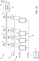
- Fig. 1a illustrates a signal generator 2.
- the signal generator 2 comprises a shift register 5 and a clock signal generator 4 and is configured to generate an amplitude sweep.
- the signal generator 2 is an RF transmitter.
- Each bit 6 of the shift register controls a respective power amplifier (PA) unit 8.
- PA power amplifier
- the PA units 8 form a set of control components, where each PA unit 8, i.e., control component, of the set of control components is arranged to be switchably activated in parallel in the signal generator 2.
- all PA units 6, when activated generate the same power P step .
- the switching may for example occur through transistors, such as MOSFET transistors.
- each PA unit 6 is fed with an RF signal 12 generated by an RF signal generator (not shown).
- the RF signal 12 is amplified by each activated PA unit 6.
- the PA units 6 are connected in parallel and fed into a matching network 12, which feeds a transmitting antenna 16.
- the amplitude of the signal generator will be proportional to the square root of the total power P of the PA units 6, which in the case of all PA units 6 having the same power P step will amount to the number of activated PA units 6 n multiplied by P step .
- the amplitude of the generated signal has an intrinsic dependence on the number of PA units 6 activated.
- the specific signal generator configuration illustrated in Fig. 1a is not the only possibility. Rather, use of a shift register controlled by a time-modulated clock signal is applicable to any signal generator circuitry where the generated amplitude depends on a number of activated control components.
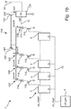
- Fig. 1b illustrates an alternative configuration.
- a signal generator 2 is an RF transmitter and comprises a shift register 5 and a clock signal generator 4 and is configured to generate an amplitude sweep.
- each bit 6 of the shift register controls a respective current source 8, which, if in an activated state, generates a contributor current I contr .
- the contributor currents of each activated current source 8 add up to a total current amounting to I contr times the number n of activated current sources 8.
- a current mirror 118 comprising a first transistor 120 and a second transistor 122, as a bias current I out , which controls an output stage in the form of a PA unit 124, which amplifies an RF signal 12 generated by an RF signal generator (not shown).
- the output power of the PA unit 124 is controlled by the bias current I out .
- the current sources 108 form a set of control components, where each current source 108, i.e., control component, of the set of control components is arranged to be switchably activated in parallel in the signal generator 2 and the amplitude of the generated signal has an intrinsic dependence on the number of current sources 108 activated.
- Each current source 108 comprises a resistor 114 in series with a transistor 116.
- the transistor 116 of each current source 8 is controlled by a respective bit 6 of the switch register 5.
- the shift register is thus embedded in the signal generator 2. This allows one to have the number of control wires independent of the number of control components 8, 108. Compared to, for example, a line-column decoder setup, the number of wires required to control the signal generator 2 is reduced to two, independent of the number of control components implemented. Reducing the number of control wires allow to reduce the power consumption of the signal generator 2.
- each bit 6 controls the activation of the respective control component 8 and is connected to the input of the next bit 6.
- the input 8 of the first bit 6, marked “up_down”, is used for shifting bits into the switch register, while the same clock signal line 10, marked “ck_mod”, is connected to all bits 6 of the shift register.
- the control components are arranged to be activated or deactivated in a pre-determined order by shifting, respectively, activation bits or de-activation bits into the shift register.
- the "up_down” line allows one to pass “up-ramping” or “down-ramping" ("0" or “1") bits into the shift register controlling the control component 6. This will result in, respectively, an increase or decrease of the signal amplitude.
- "ck_mod” is the clock signal which defines the slope of the amplitude modulation.
- a clock signal generator 4 is connected to the clock signal line 10 "ck_mod". It is configured to output a time-modulated clock signal.
- the clock signal generator 4 may be implemented using a clock and a counter, such that the period counted by the counter, and thus the period of the output clock signal, follows a programmed polynomial, as will be explained in the following.
- Fig. 2a shows a signal amplitude as a function of time for the signal generator 2, where, in this example, activation bits are shifted into the shift register 5 at regularly spaced intervals in time, as controlled by the clock line 10. Accordingly, the signal amplitude exhibits a stepping behavior at regular time intervals, reflecting a successive activation of control components. Due to the non-linear dependence of the signal amplitude on the number of activated control components 6, the amplitude sweep as a function of time will be non-linear as well, giving the result that the amplitude step is different for each additional control component connected, due to the non-linear dependence of the signal amplitude on the number of activated control components.
- Fig 2a shows a generic non linearity for illustration, however, as noted above, as in the signal generator of Fig. 1a , typically there is a square root dependence on the number of connected control components.
- Fig. 2b shows a time domain compensation which allows to compensate the amplitude non-linearity of the signal generator during an amplitude sweep, whereby a time-modulated clock signal 10 "ck_mod" is generated and output by the clock generator 4.
- This time-modulated signal has an amplitude variation as a function of time that compensates for the non-linearity of the signal generator 2.
- the frequency of the "ck_mod" clock is adjusted during an amplitude sweep based on the profile of the signal which is to be linearized.
- Fig. 2b shows an example of the clock frequency, i.e., inverse of the time between two consecutive leading edges of the clock signal 10, as a function of time.
- the clock frequency decreases as a function of time during the amplitude sweep, corresponding to increasing time between each clock signal 10 leading edge.
- determining the appropriate time between pulses on the clock signal 10 is a straightforward calculation for the skilled person.
- Fig. 2c shows with a dashed line the signal amplitude as a function of time when the clock signal of Fig. 2b is applied to the switch register 5.
- the non-linearity of Fig. 2a (shown with a dotted line for comparison) is compensated for, within the resolution provided by the step-wise activation of control components 6, with good accuracy approximating a linear sweep shown with a solid line.
- a time domain compensation allows to have a scalable and portable system which can compensate for amplitude sweep non-linearity.
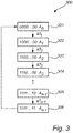
- Fig 3 shows a typical procedure 300 for generating an amplitude sweep.
- Each block shows the N bits of the shift register and the signal amplitude.
- the procedure may for example be implemented in hardware calculating a polynomial approximating equations 2 and 3 above, or in a microcontroller.
- the amplitude sweep is started by initializing the shift register 5 (cf. Fig. 1 ) by pushing deactivation ("0") bits into all bits of the shift register 5, so that none of the control component 6 are activated, the signal generator outputting a signal with a first amplitude A 0 .
- a first activation bit (“1" is pushed into the shift register, activating a first control component in the signal generator, changing the signal amplitude in a step-wise fashion to a second amplitude A 1 .
- the time ⁇ T 0 is chosen so that the step in signal amplitude A 1 -A 0 matches the desired time profile of the generated amplitude sweep, so the step-wise signal amplitude output matches the desired time profile of the generated amplitude sweep.
- a second activation bit (“1" is pushed into the shift register, activating a second control component in the signal generator, so that two control components now are activated, changing the signal amplitude to a third amplitude A 2 , with the time ⁇ T 2 similarly chosen so the step in signal amplitude to A 2 matches the desired time profile.
- This is repeated in blocks 303, 304, and 305, until the shift register, in block 306, is filled with activation ("1") bits, corresponding to all control components being activated.
- the amplitude sweep may then, optionally, be repeated by returning to block 301.
- activation bits are pushed into the shift register, typically resulting in an upward sweep in signal amplitude in the case of a square root dependence of the signal amplitude.
- the description is equally valid, mutatis mutandis, in the case of pushing deactivation bits into the shift register.
- the times between clock signals ⁇ T 0 , ⁇ T 1 , ⁇ T 2 ... will successively get shorter, corresponding to an increase in clock signal frequency, in the case of pushing activation bits into the shift register and generating an upward linear amplitude sweep, and successively longer, corresponding to a decrease in clock signal frequency, in the case of pushing deactivation bits into the shift register and generating a downward linear amplitude sweep.
Landscapes
- Engineering & Computer Science (AREA)
- Physics & Mathematics (AREA)
- General Physics & Mathematics (AREA)
- Theoretical Computer Science (AREA)
- Computational Mathematics (AREA)
- Mathematical Analysis (AREA)
- Mathematical Optimization (AREA)
- Pure & Applied Mathematics (AREA)
- General Engineering & Computer Science (AREA)
- Power Engineering (AREA)
- Amplifiers (AREA)
Abstract
Description
- The present inventive concept relates to a signal generator configured to generate a signal with an amplitude sweep. Further, the present inventive concept relates to a method of generating a signal with an amplitude sweep.
- Signal generators configured to generate an amplitude sweep are, for example, useful for biomedical applications, such as biomedical radar systems. This requires a fine resolution, circuit area efficiency, and low power. For example, such amplitude sweeps may be generated using switchable parallel power amplifier (PA) units or by switchable resistors in the signal generator circuitry.
- An objective of the present inventive concept is to provide a signal generator configured to generate an amplitude sweep with high accuracy with respect to a desired time profile of the amplitude sweep while retaining low circuit complexity. Additionally or alternatively, an objective is to provide a signal generator configured to generate an amplitude sweep with a high degree of linearity.
- According to an aspect of the present inventive concept, there is provided a signal generator configured to generate a signal with an amplitude sweep, said signal generator having circuitry comprising: a set of control components, each control component of said set of control components being arranged to be switchably activated in parallel in said circuitry so that an amplitude of said signal has an intrinsic dependence on the number of said control components activated; a shift register controllable by a clock line and comprising a number of bits, each bit of said number of bits controlling activation of a respective control component of said set of control components so that said control components are arranged to be activated or de-activated in a pre-determined order by shifting, respectively, activation or de-activation bits into said shift register, wherein said shifting is paced by said clock line; and a clock signal generator configured to output a clock signal with a time modulation on said clock line.
- The present inventive concept is applicable to any signal generator arrangement where the amplitude of the signal has an intrinsic dependence on the number of control components activated. The control components may for example be power amplifier (PA) units, resistors, or current sources.
- The bits comprised in the shift register may typically be input into the shift register using a data line. Upon an activation signal on the clock line, which for example may be a leading edge of the clock signal, the signal on the data line is stored in the first bit of the shift register, while the bit previously stored there is moved to the second bit, and so on. If, for example, the shift register starts in a state with all deactivation bits (typically "0" bits), meaning that no control components are connected in the circuit, an activation bit (typically a "1" bit) may be shifted into the first bit of the shift register upon activation of the clock signal, switching the corresponding control component into the circuit, simultaneously changing the signal amplitude. Upon the next leading edge of the clock signal, another one bit may be shifted into the shift register, so that the first two bits now are activation bits, while the rest of the bits are deactivation bits, further changing the amplitude of the signal generator, and so on. Thus, pacing of this shifting, i.e., the time between the shifts in signal amplitude, is controlled by the clock line. This typically leads to a sweep towards decreasing amplitude.
- In another equally possible mode of operation, the shift register may start in a state with all activation bits, meaning that all control components of the set of control components are connected in the circuit. Deactivation bits may then successively be shifted into the shift register, typically leading to a sweep towards decreasing amplitude.
- The intrinsic dependence of the amplitude of the signal on the number of activated control components may be either linear or non-linear, depending on the kind of control components used and how they are arranged. In a general case, the signal generator is configured to generate the amplitude sweep with a specific time dependence, the time modulation being based on the specific time dependence of said amplitude sweep in relation to said intrinsic dependence of the amplitude of the signal on the number of control components activated, so that the signal generator generates the amplitude sweep with the specific time dependence. In other words, the time modulation may be adjusted based on the time profile of a desired amplitude sweep, so that the signal generator generates the amplitude sweep with that desired time dependence.
- As one example, the desired time dependence of the amplitude sweep may be a linear ramp and the intrinsic dependence of the amplitude of the signal on the number of activated control components may be non-linear. The time modulation of the clock signal will then serve to compensate for any non-linearity relative to this desired linear ramp. Such amplitude non-linearity may, for example, come from systems where power, rather than amplitude, adds up linearly, leading to a square-root dependence of the generated signal amplitude as a function the number control components activated. It may also be due to second-order effects such as supply resistance or internal resistance.
- In another example, the intrinsic dependence of the amplitude of the signal on the number of activated control components may be linear, or close to linear, while the desired time dependence of the amplitude of the generator signal is non-linear.
- Desired non-linear amplitude sweeps may for example, as a function of time, be exponential, i.e., the amplitude being linear as expressed in decibels, have a square root time dependence, or be a polynomial, such as a square function.
- By time-modulating the clock signal controlling the shift register, i.e., letting it have a varying time between activation signals on the clock line, such as a gradually increasing or decreasing clock frequency, a desired amplitude sweep may be achieved while at the same time allowing for a relatively low circuit complexity, as only two control lines - the data line and the control line - are needed. Further, this approach is well suited for fast amplitude ramping.
- According to an embodiment, the signal generator is an RF transmitter and each control component of the set of control components is a power amplifier unit. In this case, the power output of each of the power amplifier units will then add up in the output signal.
- For example, in a case of each power amplifier unit generating the same power, the amplitude of the signal output by the signal generator may be proportional, or roughly proportional, to the square root of the number of activated power amplifier units. If a linear amplitude sweep is desired, when generating an amplitude sweep, the time-modulated clock signal will be able to compensate for this non-linearity. Hereby, good sweep linearity can be achieved with a simple design. Further, this allows for the use of simpler and more efficient power amplifier units, as the power of each power amplifier unit is considerably smaller than the total maximum power of the RF transmitter, while still allowing for good sweep linearity though the time-modulated clock signal.
- According to an embodiment, the signal generator further comprises an output stage configured to output the signal, the output stage being controlled by a bias current generated by a bias current source controlled by the set of control components. Typically, the signal generator is an RF transmitter and the output stage is a power amplifier unit. In this case, non-linearity in the generated amplitude sweep is due to non-linearity between the bias current and the amplitude output by the output stage. When generating an amplitude sweep, the time-modulated clock signal approach will be equally well suited to compensate for this non-linearity, again allowing for good sweep linearity with a relatively simple circuit design.
- According to an embodiment, each control component of the set of control components is a current source configured to generate a contributor current, a sum of each the contributor current controlling the bias current source. This allows for a flexible, yet simple, way of controlling the bias current source.
- According to an embodiment, the bias current source is a current mirror. This leads to addition of the contributor currents to form the bias current in a reliable way.
- According to an embodiment, each control component of the set of control components comprises a resistor in series with a transistor controlled by a bit of the shift register. This is a simple, yet reliable, implementation of a current source.
- According to another aspect of the present inventive concept, there is provided a method of generating a signal with an amplitude sweep, the method comprising: shifting activation or de-activation bits into a shift register, the shift register comprising a number of bits, each bit of the number of bits controlling activation of a respective control component of a set of control components in parallel in circuitry of a signal generator, the control components being activated or de-activated in a pre-determined order by the shifting of said activation or deactivation bits, the amplitude of the signal having an intrinsic dependence on the number of the control components activated, wherein the shifting is paced by a clock signal having a time modulation.
- This aspect may generally present the same or corresponding advantages as the former aspect.
- The above, as well as additional objects, features and advantages of the present inventive concept, will be better understood through the following illustrative and non-limiting detailed description, with reference to the appended drawings. In the drawings like reference numerals will be used for like elements unless stated otherwise.
-
Figs 1a and1b are schematics of signal generators, each with an embedded switch register, the clock signal of which is controlled by a clock signal generator. -
Fig. 2a shows the amplitude sweep of the signal generator when not corrected for non-linearity. -
Fig. 2b shows the inverse of the time between two clock signal leading edges as a function of time for a time-modulated clock signal compensating for non-linearity. -
Fig. 2c shows the non-linear profile ofFig. 2a , the linearized signal using the time-modulated clock signal ofFig. 2b , and the resulting amplitude sweep compared to an ideal linear ramp. -
Fig. 3 shows a typical procedure for generating an amplitude sweep. -
Fig. 1a illustrates asignal generator 2. Thesignal generator 2 comprises ashift register 5 and aclock signal generator 4 and is configured to generate an amplitude sweep. In this embodiment, thesignal generator 2 is an RF transmitter. Eachbit 6 of the shift register controls a respective power amplifier (PA)unit 8. Thus, thePA units 8 form a set of control components, where eachPA unit 8, i.e., control component, of the set of control components is arranged to be switchably activated in parallel in thesignal generator 2. Typically, allPA units 6, when activated, generate the same power P step. The switching may for example occur through transistors, such as MOSFET transistors. Further, eachPA unit 6 is fed with anRF signal 12 generated by an RF signal generator (not shown). TheRF signal 12 is amplified by each activatedPA unit 6. ThePA units 6 are connected in parallel and fed into amatching network 12, which feeds a transmittingantenna 16. In this specific embodiment, the amplitude of the signal generator will be proportional to the square root of the total power P of thePA units 6, which in the case of allPA units 6 having the same power P step will amount to the number of activated PA units 6 n multiplied by P step. Thus, the amplitude of the generated signal has an intrinsic dependence on the number ofPA units 6 activated.
However, the specific signal generator configuration illustrated inFig. 1a is not the only possibility. Rather, use of a shift register controlled by a time-modulated clock signal is applicable to any signal generator circuitry where the generated amplitude depends on a number of activated control components. -
Fig. 1b illustrates an alternative configuration. As inFig. 1a , asignal generator 2 is an RF transmitter and comprises ashift register 5 and aclock signal generator 4 and is configured to generate an amplitude sweep. However, here, eachbit 6 of the shift register controls a respectivecurrent source 8, which, if in an activated state, generates a contributor current I contr. The contributor currents of each activatedcurrent source 8 add up to a total current amounting to I contr times the number n of activatedcurrent sources 8. This total current is mirrored by acurrent mirror 118, comprising afirst transistor 120 and asecond transistor 122, as a bias current I out, which controls an output stage in the form of aPA unit 124, which amplifies anRF signal 12 generated by an RF signal generator (not shown). The output power of thePA unit 124 is controlled by the bias current I out. Thus, thecurrent sources 108 form a set of control components, where eachcurrent source 108, i.e., control component, of the set of control components is arranged to be switchably activated in parallel in thesignal generator 2 and the amplitude of the generated signal has an intrinsic dependence on the number ofcurrent sources 108 activated. Eachcurrent source 108 comprises aresistor 114 in series with atransistor 116. Thetransistor 116 of eachcurrent source 8 is controlled by arespective bit 6 of theswitch register 5. - In both
Fig 1a andFig. 1b , the shift register is thus embedded in thesignal generator 2. This allows one to have the number of control wires independent of the number ofcontrol components signal generator 2 is reduced to two, independent of the number of control components implemented. Reducing the number of control wires allow to reduce the power consumption of thesignal generator 2. - Again with reference to both
Figs 1a and1b , the output of eachbit 6 controls the activation of therespective control component 8 and is connected to the input of thenext bit 6. Theinput 8 of thefirst bit 6, marked "up_down", is used for shifting bits into the switch register, while the sameclock signal line 10, marked "ck_mod", is connected to allbits 6 of the shift register. Thus, the control components are arranged to be activated or deactivated in a pre-determined order by shifting, respectively, activation bits or de-activation bits into the shift register. The "up_down" line allows one to pass "up-ramping" or "down-ramping" ("0" or "1") bits into the shift register controlling thecontrol component 6. This will result in, respectively, an increase or decrease of the signal amplitude. "ck_mod" is the clock signal which defines the slope of the amplitude modulation. - A
clock signal generator 4 is connected to theclock signal line 10 "ck_mod". It is configured to output a time-modulated clock signal. Theclock signal generator 4 may be implemented using a clock and a counter, such that the period counted by the counter, and thus the period of the output clock signal, follows a programmed polynomial, as will be explained in the following. -
Fig. 2a shows a signal amplitude as a function of time for thesignal generator 2, where, in this example, activation bits are shifted into theshift register 5 at regularly spaced intervals in time, as controlled by theclock line 10. Accordingly, the signal amplitude exhibits a stepping behavior at regular time intervals, reflecting a successive activation of control components. Due to the non-linear dependence of the signal amplitude on the number of activatedcontrol components 6, the amplitude sweep as a function of time will be non-linear as well, giving the result that the amplitude step is different for each additional control component connected, due to the non-linear dependence of the signal amplitude on the number of activated control components.Fig 2a shows a generic non linearity for illustration, however, as noted above, as in the signal generator ofFig. 1a , typically there is a square root dependence on the number of connected control components. -
Fig. 2b shows a time domain compensation which allows to compensate the amplitude non-linearity of the signal generator during an amplitude sweep, whereby a time-modulatedclock signal 10 "ck_mod" is generated and output by theclock generator 4. This time-modulated signal has an amplitude variation as a function of time that compensates for the non-linearity of thesignal generator 2. This allows one to compensate for the non-linearity of the signal generator. In other words, the frequency of the "ck_mod" clock is adjusted during an amplitude sweep based on the profile of the signal which is to be linearized.Fig. 2b shows an example of the clock frequency, i.e., inverse of the time between two consecutive leading edges of theclock signal 10, as a function of time. In this example, to compensate for the non-linearity of the signal amplitude (cf.Fig. 2a ) the clock frequency decreases as a function of time during the amplitude sweep, corresponding to increasing time between eachclock signal 10 leading edge. - Given a desired amplitude sweep as a function of time - for example, a linear function, an exponential, a square root function, or a polynomial, such as a square function - and the intrinsic dependence of the signal amplitude on the number of activated control components 6 (cf.
Fig 1 ), determining the appropriate time between pulses on theclock signal 10 is a straightforward calculation for the skilled person. For example, in a linear ramp between amplitudes AA and AB from time t = 0 to time t = T, the signal amplitude ft at time t can be written


- To find appropriate pulse times, one may substitute An of equation 3 for At in
equation 2. The resulting formula may be approximated by a polynomial, reducing hardware complexity, and allowing for a fast, flexible, and low-power clock signal generator. -
Fig. 2c shows with a dashed line the signal amplitude as a function of time when the clock signal ofFig. 2b is applied to theswitch register 5. The non-linearity ofFig. 2a (shown with a dotted line for comparison) is compensated for, within the resolution provided by the step-wise activation ofcontrol components 6, with good accuracy approximating a linear sweep shown with a solid line. Thus a time domain compensation allows to have a scalable and portable system which can compensate for amplitude sweep non-linearity. -
Fig 3 shows atypical procedure 300 for generating an amplitude sweep. Each block shows the N bits of the shift register and the signal amplitude. The procedure may for example be implemented in hardware calculating apolynomial approximating equations 2 and 3 above, or in a microcontroller. - In
block 301, the amplitude sweep is started by initializing the shift register 5 (cf.Fig. 1 ) by pushing deactivation ("0") bits into all bits of theshift register 5, so that none of thecontrol component 6 are activated, the signal generator outputting a signal with a first amplitude A0. - In
block 302, on leading edge of theclock signal 10, after a time ΔT0, a first activation bit ("1") is pushed into the shift register, activating a first control component in the signal generator, changing the signal amplitude in a step-wise fashion to a second amplitude A1. The time ΔT0 is chosen so that the step in signal amplitude A1-A0 matches the desired time profile of the generated amplitude sweep, so the step-wise signal amplitude output matches the desired time profile of the generated amplitude sweep. - Similarly, in
block 302, after a further time ΔT1, a second activation bit ("1") is pushed into the shift register, activating a second control component in the signal generator, so that two control components now are activated, changing the signal amplitude to a third amplitude A2, with the time ΔT 2 similarly chosen so the step in signal amplitude to A2 matches the desired time profile. This is repeated inblocks block 306, is filled with activation ("1") bits, corresponding to all control components being activated. - The amplitude sweep may then, optionally, be repeated by returning to block 301.
- In this example, activation bits are pushed into the shift register, typically resulting in an upward sweep in signal amplitude in the case of a square root dependence of the signal amplitude. However, the description is equally valid, mutatis mutandis, in the case of pushing deactivation bits into the shift register. In the case of generating a linear amplitude sweep, the times between clock signals ΔT0 , ΔT1, ΔT2 ... will successively get shorter, corresponding to an increase in clock signal frequency, in the case of pushing activation bits into the shift register and generating an upward linear amplitude sweep, and successively longer, corresponding to a decrease in clock signal frequency, in the case of pushing deactivation bits into the shift register and generating a downward linear amplitude sweep.
- In the above the inventive concept has mainly been described with reference to a limited number of examples. However, as is readily appreciated by a person skilled in the art, other examples than the ones disclosed above are equally possible within the scope of the inventive concept, as defined by the appended claims.
Claims (11)
- A signal generator (2) configured to generate a signal with an amplitude sweep, said signal generator having circuitry comprising:a set of control components (8, 108), each control component of said set of control components being arranged to be switchably activated in parallel in said circuitry so that an amplitude of said signal has an intrinsic dependence on the number of said control components activated;a shift register (5) controllable by a clock line and comprising a number of bits (6), each bit (6) of said number of bits (6) controlling activation of a respective control component (8, 108) of said set of control components so that said control components (8, 108) are arranged to be activated or de-activated in a pre-determined order by shifting, respectively, activation or de-activation bits into said shift register, wherein said shifting is paced by said clock line; anda clock signal generator (4) configured to output a clock signal with a time modulation on said clock line.
- The signal generator of claim 1, wherein said signal generator (2) is an RF transmitter and each control component of said set of control components is a power amplifier unit (8).
- The signal generator of claim 1, said signal generator further comprising an output stage (124) configured to output said signal, said output stage being controlled by a bias current generated by a bias current source (118) controlled by said set of control components (108).
- The signal generator of claim 3, wherein said signal generator is an RF transmitter and said output stage (124) is a power amplifier unit (124).
- The signal generator of any one of claims 3 or 4, wherein each control component (108) of said set of control components (108) is a current source (108) configured to generate a contributor current, a sum of each said contributor current controlling said bias current source (118).
- The signal generator of any one of claims 3-5, wherein said bias current source (108) is a current mirror (108).
- The signal generator of any one of claims 3-6, wherein each control component (108) of said set of control components (108) comprises a resistor (114) in series with a transistor (116) controlled by a bit (6) of said shift register.
- The signal generator of any one of claims 1-7, wherein said signal generator (2) is configured to generate said amplitude sweep with a specific time dependence, said time modulation being based on said specific time dependence of said amplitude sweep in relation to said intrinsic dependence of said amplitude of said signal on the number of control components activated, so that said signal generator generates said amplitude sweep with said specific time dependence.
- The signal generator of claim 8, wherein said specific time dependence of said amplitude sweep is a linear ramp.
- The signal generator of any one of claims 1-9, wherein said amplitude sweep is towards increasing amplitude.
- A method of generating a signal with an amplitude sweep, said method comprising:
shifting activation or de-activation bits into a shift register (5), said shift register (5) comprising a number of bits, each bit (6) of said number of bits controlling activation of a respective control component (8, 108) of a set of control components (8, 109) in parallel in circuitry of a signal generator, said control components (8, 108) being activated or de-activated in a pre-determined order by said shifting of said activation or deactivation bits, said amplitude of said signal having an intrinsic dependence on the number of said control components activated, wherein said shifting is paced by a clock signal having a time modulation.
Priority Applications (2)
| Application Number | Priority Date | Filing Date | Title |
|---|---|---|---|
| EP18212401.6A EP3667913B1 (en) | 2018-12-13 | 2018-12-13 | Amplitude sweep generator and method |
| US16/714,128 US11088664B2 (en) | 2018-12-13 | 2019-12-13 | Amplitude sweep generator and method |
Applications Claiming Priority (1)
| Application Number | Priority Date | Filing Date | Title |
|---|---|---|---|
| EP18212401.6A EP3667913B1 (en) | 2018-12-13 | 2018-12-13 | Amplitude sweep generator and method |
Publications (2)
| Publication Number | Publication Date |
|---|---|
| EP3667913A1 true EP3667913A1 (en) | 2020-06-17 |
| EP3667913B1 EP3667913B1 (en) | 2026-01-21 |
Family
ID=64665477
Family Applications (1)
| Application Number | Title | Priority Date | Filing Date |
|---|---|---|---|
| EP18212401.6A Active EP3667913B1 (en) | 2018-12-13 | 2018-12-13 | Amplitude sweep generator and method |
Country Status (2)
| Country | Link |
|---|---|
| US (1) | US11088664B2 (en) |
| EP (1) | EP3667913B1 (en) |
Citations (5)
| Publication number | Priority date | Publication date | Assignee | Title |
|---|---|---|---|---|
| US3893115A (en) * | 1974-01-25 | 1975-07-01 | Us Navy | Sweep and memory control circuit |
| FR2336831A1 (en) * | 1975-12-24 | 1977-07-22 | Texas Instruments France | Low frequency tone generator - for telephone and general communications uses quartz clock with three frequency dividers |
| US20090080241A1 (en) * | 2007-09-26 | 2009-03-26 | Gutala Ravi P | Programming a phase change memory |
| EP2251976A1 (en) * | 2009-05-12 | 2010-11-17 | ST-Ericsson SA | RF amplifier with digital filter for polar transmitter |
| US20150015338A1 (en) * | 2012-12-25 | 2015-01-15 | Panasonic Corporation | Power amplifier |
Family Cites Families (1)
| Publication number | Priority date | Publication date | Assignee | Title |
|---|---|---|---|---|
| JP5252212B2 (en) * | 2009-03-12 | 2013-07-31 | ルネサスエレクトロニクス株式会社 | Semiconductor device for signal amplification |
-
2018
- 2018-12-13 EP EP18212401.6A patent/EP3667913B1/en active Active
-
2019
- 2019-12-13 US US16/714,128 patent/US11088664B2/en active Active
Patent Citations (5)
| Publication number | Priority date | Publication date | Assignee | Title |
|---|---|---|---|---|
| US3893115A (en) * | 1974-01-25 | 1975-07-01 | Us Navy | Sweep and memory control circuit |
| FR2336831A1 (en) * | 1975-12-24 | 1977-07-22 | Texas Instruments France | Low frequency tone generator - for telephone and general communications uses quartz clock with three frequency dividers |
| US20090080241A1 (en) * | 2007-09-26 | 2009-03-26 | Gutala Ravi P | Programming a phase change memory |
| EP2251976A1 (en) * | 2009-05-12 | 2010-11-17 | ST-Ericsson SA | RF amplifier with digital filter for polar transmitter |
| US20150015338A1 (en) * | 2012-12-25 | 2015-01-15 | Panasonic Corporation | Power amplifier |
Also Published As
| Publication number | Publication date |
|---|---|
| EP3667913B1 (en) | 2026-01-21 |
| US20200195211A1 (en) | 2020-06-18 |
| US11088664B2 (en) | 2021-08-10 |
Similar Documents
| Publication | Publication Date | Title |
|---|---|---|
| US5045800A (en) | Pulse width modulator control circuit | |
| US4870665A (en) | Digital pulse generator having a programmable pulse width and a pulse repetition interval | |
| US9325241B2 (en) | Dead-time compensation in a power supply system | |
| JP5157959B2 (en) | Class D amplifier | |
| EP3849083A1 (en) | Gate driver | |
| US9634656B2 (en) | Current driver circuit | |
| US20120126901A1 (en) | Programmable electro-magnetic-interference (emi) reduction with enhanced noise immunity and process tolerance | |
| US20240106394A1 (en) | Power supply circuit, power supply method, audio power amplifier and integrated circuit | |
| CN106656109B (en) | Digital clock duty cycle correction | |
| CN100581052C (en) | Automatic gain control system with self-adaptive climb and decay time | |
| EP2802074B1 (en) | Amplifier circuit and amplification method | |
| EP3667913B1 (en) | Amplitude sweep generator and method | |
| US8730694B2 (en) | Signal transmission arrangement with a transformer | |
| US10938393B2 (en) | Frequency sweep generator and method | |
| KR101035743B1 (en) | Impulse Generation Circuit | |
| JP4899172B2 (en) | Pulse mode amplifier two peak power level control method and apparatus | |
| JP5157960B2 (en) | Class D amplifier | |
| US7054360B2 (en) | Method and apparatus for generating pulse width modulated waveforms | |
| US6191626B1 (en) | Method and apparatus for compensating input threshold variations on input buffers | |
| JP2025181249A (en) | Switching Circuit | |
| JP2010279575A (en) | Transmission control device for ultrasonic diagnostic equipment | |
| EP0712205A2 (en) | Fixed-interval timing circuit and method | |
| HUT64653A (en) | Method and apparatus for converting time into voltage | |
| JPH04219013A (en) | Pulse width adjustment circuit | |
| JPS5941638Y2 (en) | monostable multivibrator |
Legal Events
| Date | Code | Title | Description |
|---|---|---|---|
| PUAI | Public reference made under article 153(3) epc to a published international application that has entered the european phase |
Free format text: ORIGINAL CODE: 0009012 |
|
| STAA | Information on the status of an ep patent application or granted ep patent |
Free format text: STATUS: THE APPLICATION HAS BEEN PUBLISHED |
|
| AK | Designated contracting states |
Kind code of ref document: A1 Designated state(s): AL AT BE BG CH CY CZ DE DK EE ES FI FR GB GR HR HU IE IS IT LI LT LU LV MC MK MT NL NO PL PT RO RS SE SI SK SM TR |
|
| AX | Request for extension of the european patent |
Extension state: BA ME |
|
| STAA | Information on the status of an ep patent application or granted ep patent |
Free format text: STATUS: REQUEST FOR EXAMINATION WAS MADE |
|
| 17P | Request for examination filed |
Effective date: 20201214 |
|
| RBV | Designated contracting states (corrected) |
Designated state(s): AL AT BE BG CH CY CZ DE DK EE ES FI FR GB GR HR HU IE IS IT LI LT LU LV MC MK MT NL NO PL PT RO RS SE SI SK SM TR |
|
| STAA | Information on the status of an ep patent application or granted ep patent |
Free format text: STATUS: EXAMINATION IS IN PROGRESS |
|
| 17Q | First examination report despatched |
Effective date: 20220401 |
|
| GRAP | Despatch of communication of intention to grant a patent |
Free format text: ORIGINAL CODE: EPIDOSNIGR1 |
|
| STAA | Information on the status of an ep patent application or granted ep patent |
Free format text: STATUS: GRANT OF PATENT IS INTENDED |
|
| INTG | Intention to grant announced |
Effective date: 20250814 |
|
| GRAS | Grant fee paid |
Free format text: ORIGINAL CODE: EPIDOSNIGR3 |
|
| GRAA | (expected) grant |
Free format text: ORIGINAL CODE: 0009210 |
|
| STAA | Information on the status of an ep patent application or granted ep patent |
Free format text: STATUS: THE PATENT HAS BEEN GRANTED |
|
| AK | Designated contracting states |
Kind code of ref document: B1 Designated state(s): AL AT BE BG CH CY CZ DE DK EE ES FI FR GB GR HR HU IE IS IT LI LT LU LV MC MK MT NL NO PL PT RO RS SE SI SK SM TR |
|
| REG | Reference to a national code |
Ref country code: CH Ref legal event code: F10 Free format text: ST27 STATUS EVENT CODE: U-0-0-F10-F00 (AS PROVIDED BY THE NATIONAL OFFICE) Effective date: 20260121 |
|
| REG | Reference to a national code |
Ref country code: IE Ref legal event code: FG4D |
|
| REG | Reference to a national code |
Ref country code: DE Ref legal event code: R096 Ref document number: 602018088683 Country of ref document: DE |
|
| P01 | Opt-out of the competence of the unified patent court (upc) registered |
Free format text: CASE NUMBER: UPC_APP_0004242_3667913/2026 Effective date: 20260205 |