EP3667906A1 - Flying capacitor voltage control in an amplifier - Google Patents
Flying capacitor voltage control in an amplifier Download PDFInfo
- Publication number
- EP3667906A1 EP3667906A1 EP19215256.9A EP19215256A EP3667906A1 EP 3667906 A1 EP3667906 A1 EP 3667906A1 EP 19215256 A EP19215256 A EP 19215256A EP 3667906 A1 EP3667906 A1 EP 3667906A1
- Authority
- EP
- European Patent Office
- Prior art keywords
- vcf
- voltage
- stage
- signal
- input signal
- Prior art date
- Legal status (The legal status is an assumption and is not a legal conclusion. Google has not performed a legal analysis and makes no representation as to the accuracy of the status listed.)
- Granted
Links
Images


Classifications
-
- H—ELECTRICITY
- H03—ELECTRONIC CIRCUITRY
- H03F—AMPLIFIERS
- H03F3/00—Amplifiers with only discharge tubes or only semiconductor devices as amplifying elements
- H03F3/005—Amplifiers with only discharge tubes or only semiconductor devices as amplifying elements using switched capacitors, e.g. dynamic amplifiers; using switched capacitors as resistors in differential amplifiers
-
- H—ELECTRICITY
- H03—ELECTRONIC CIRCUITRY
- H03F—AMPLIFIERS
- H03F1/00—Details of amplifiers with only discharge tubes, only semiconductor devices or only unspecified devices as amplifying elements
- H03F1/30—Modifications of amplifiers to reduce influence of variations of temperature or supply voltage or other physical parameters
-
- H—ELECTRICITY
- H03—ELECTRONIC CIRCUITRY
- H03F—AMPLIFIERS
- H03F1/00—Details of amplifiers with only discharge tubes, only semiconductor devices or only unspecified devices as amplifying elements
- H03F1/26—Modifications of amplifiers to reduce influence of noise generated by amplifying elements
-
- H—ELECTRICITY
- H02—GENERATION; CONVERSION OR DISTRIBUTION OF ELECTRIC POWER
- H02M—APPARATUS FOR CONVERSION BETWEEN AC AND AC, BETWEEN AC AND DC, OR BETWEEN DC AND DC, AND FOR USE WITH MAINS OR SIMILAR POWER SUPPLY SYSTEMS; CONVERSION OF DC OR AC INPUT POWER INTO SURGE OUTPUT POWER; CONTROL OR REGULATION THEREOF
- H02M1/00—Details of apparatus for conversion
- H02M1/0067—Converter structures employing plural converter units, other than for parallel operation of the units on a single load
- H02M1/0077—Plural converter units whose outputs are connected in series
-
- H—ELECTRICITY
- H02—GENERATION; CONVERSION OR DISTRIBUTION OF ELECTRIC POWER
- H02M—APPARATUS FOR CONVERSION BETWEEN AC AND AC, BETWEEN AC AND DC, OR BETWEEN DC AND DC, AND FOR USE WITH MAINS OR SIMILAR POWER SUPPLY SYSTEMS; CONVERSION OF DC OR AC INPUT POWER INTO SURGE OUTPUT POWER; CONTROL OR REGULATION THEREOF
- H02M3/00—Conversion of DC power input into DC power output
- H02M3/02—Conversion of DC power input into DC power output without intermediate conversion into AC
- H02M3/04—Conversion of DC power input into DC power output without intermediate conversion into AC by static converters
- H02M3/06—Conversion of DC power input into DC power output without intermediate conversion into AC by static converters using resistors or capacitors, e.g. potential divider
- H02M3/07—Conversion of DC power input into DC power output without intermediate conversion into AC by static converters using resistors or capacitors, e.g. potential divider using capacitors charged and discharged alternately by semiconductor devices with control electrode, e.g. charge pumps
-
- H—ELECTRICITY
- H02—GENERATION; CONVERSION OR DISTRIBUTION OF ELECTRIC POWER
- H02M—APPARATUS FOR CONVERSION BETWEEN AC AND AC, BETWEEN AC AND DC, OR BETWEEN DC AND DC, AND FOR USE WITH MAINS OR SIMILAR POWER SUPPLY SYSTEMS; CONVERSION OF DC OR AC INPUT POWER INTO SURGE OUTPUT POWER; CONTROL OR REGULATION THEREOF
- H02M7/00—Conversion of AC power input into DC power output; Conversion of DC power input into AC power output
- H02M7/42—Conversion of DC power input into AC power output without possibility of reversal
- H02M7/44—Conversion of DC power input into AC power output without possibility of reversal by static converters
- H02M7/48—Conversion of DC power input into AC power output without possibility of reversal by static converters using discharge tubes with control electrode or semiconductor devices with control electrode
- H02M7/483—Converters with outputs that each can have more than two voltages levels
- H02M7/4833—Capacitor voltage balancing
-
- H—ELECTRICITY
- H02—GENERATION; CONVERSION OR DISTRIBUTION OF ELECTRIC POWER
- H02M—APPARATUS FOR CONVERSION BETWEEN AC AND AC, BETWEEN AC AND DC, OR BETWEEN DC AND DC, AND FOR USE WITH MAINS OR SIMILAR POWER SUPPLY SYSTEMS; CONVERSION OF DC OR AC INPUT POWER INTO SURGE OUTPUT POWER; CONTROL OR REGULATION THEREOF
- H02M7/00—Conversion of AC power input into DC power output; Conversion of DC power input into AC power output
- H02M7/42—Conversion of DC power input into AC power output without possibility of reversal
- H02M7/44—Conversion of DC power input into AC power output without possibility of reversal by static converters
- H02M7/48—Conversion of DC power input into AC power output without possibility of reversal by static converters using discharge tubes with control electrode or semiconductor devices with control electrode
- H02M7/483—Converters with outputs that each can have more than two voltages levels
- H02M7/4837—Flying capacitor converters
-
- H—ELECTRICITY
- H03—ELECTRONIC CIRCUITRY
- H03F—AMPLIFIERS
- H03F1/00—Details of amplifiers with only discharge tubes, only semiconductor devices or only unspecified devices as amplifying elements
- H03F1/02—Modifications of amplifiers to raise the efficiency, e.g. gliding Class A stages, use of an auxiliary oscillation
- H03F1/0205—Modifications of amplifiers to raise the efficiency, e.g. gliding Class A stages, use of an auxiliary oscillation in transistor amplifiers
- H03F1/0211—Modifications of amplifiers to raise the efficiency, e.g. gliding Class A stages, use of an auxiliary oscillation in transistor amplifiers with control of the supply voltage or current
- H03F1/0216—Continuous control
- H03F1/0222—Continuous control by using a signal derived from the input signal
-
- H—ELECTRICITY
- H03—ELECTRONIC CIRCUITRY
- H03F—AMPLIFIERS
- H03F1/00—Details of amplifiers with only discharge tubes, only semiconductor devices or only unspecified devices as amplifying elements
- H03F1/02—Modifications of amplifiers to raise the efficiency, e.g. gliding Class A stages, use of an auxiliary oscillation
- H03F1/0205—Modifications of amplifiers to raise the efficiency, e.g. gliding Class A stages, use of an auxiliary oscillation in transistor amplifiers
- H03F1/0211—Modifications of amplifiers to raise the efficiency, e.g. gliding Class A stages, use of an auxiliary oscillation in transistor amplifiers with control of the supply voltage or current
- H03F1/0216—Continuous control
- H03F1/0233—Continuous control by using a signal derived from the output signal, e.g. bootstrapping the voltage supply
-
- H—ELECTRICITY
- H03—ELECTRONIC CIRCUITRY
- H03F—AMPLIFIERS
- H03F3/00—Amplifiers with only discharge tubes or only semiconductor devices as amplifying elements
- H03F3/181—Low-frequency amplifiers, e.g. audio preamplifiers
- H03F3/183—Low-frequency amplifiers, e.g. audio preamplifiers with semiconductor devices only
-
- H—ELECTRICITY
- H03—ELECTRONIC CIRCUITRY
- H03G—CONTROL OF AMPLIFICATION
- H03G3/00—Gain control in amplifiers or frequency changers
- H03G3/20—Automatic control
-
- H—ELECTRICITY
- H03—ELECTRONIC CIRCUITRY
- H03F—AMPLIFIERS
- H03F3/00—Amplifiers with only discharge tubes or only semiconductor devices as amplifying elements
- H03F3/20—Power amplifiers, e.g. Class B amplifiers, Class C amplifiers
- H03F3/21—Power amplifiers, e.g. Class B amplifiers, Class C amplifiers with semiconductor devices only
- H03F3/217—Class D power amplifiers; Switching amplifiers
- H03F3/2171—Class D power amplifiers; Switching amplifiers with field-effect devices
-
- H—ELECTRICITY
- H03—ELECTRONIC CIRCUITRY
- H03F—AMPLIFIERS
- H03F3/00—Amplifiers with only discharge tubes or only semiconductor devices as amplifying elements
- H03F3/20—Power amplifiers, e.g. Class B amplifiers, Class C amplifiers
- H03F3/21—Power amplifiers, e.g. Class B amplifiers, Class C amplifiers with semiconductor devices only
- H03F3/217—Class D power amplifiers; Switching amplifiers
- H03F3/2173—Class D power amplifiers; Switching amplifiers of the bridge type
Definitions
- Conventional audio amplifiers sometimes include a so-called flying capacitor disposed in a respective switched output stage to drive a load.
- the flying capacitor stores an intermediate voltage value whose magnitude is a fraction of a magnitude of a main voltage rail powering the switched output stage. Presence of the flying capacitor enables a controller to apply the voltage of the flying capacitor to a load in addition to being able to apply standard voltage rails such as main power source voltage and ground to the load.
- a main voltage rail of a switched output stage of an amplifier may be 5 volts DC; the voltage on the flying capacitor may be set to 1 ⁇ 2 the main voltage rail or 2.5 volts DC.
- the so-called flying capacitor is electrically coupled across multiple switches in a switched output stage (such a sequence of series connected switches configured as a bridge circuit).
- the switches in the switched output stage can be independently controlled to produce an output voltage to drive the load.
- the switches in the output stage can be controlled (switched ON and OFF at appropriate time) to drive the load with a maximum voltage (main voltage rail) or ground reference voltage at different times.
- a respective controller is able to software between driving a load with voltages of different voltage magnitudes such as a main rail voltage, one or more intermediate or fractional voltages (stored in the one or more flying capacitors), and a ground reference voltage to produce an output voltage to power a respective load.
- a voltage stored in a flying capacitor is precisely maintained at a predetermined value. This ensures accurate generation of an output voltage.
- one drawback of the conventional implementation of a flying capacitor in an amplifier circuit is that the voltage across the flying capacitor can drift or vary with respect to a desired setpoint value. In such an instance, undesirable variations in the intermediate voltage stored in the flying capacitor (that is used to drive a respective load) results in unwanted noise or distortion in a generated output signal.
- Embodiments herein include novel ways of providing improved performance of an amplifier and generation of an output voltage.
- an amplifier includes: an input stage, a pulse width modulation stage, and a switched output stage.
- the input stage receives an input signal such as an audio signal.
- the input stage adjusts the input signal based on feedback from the switched output stage.
- the feedback is associated with the flying capacitor disposed in the switched output stage.
- the pulse width modulation stage uses the adjusted input signal or input signals to produce respective pulse width modulation signals that are subsequently used to drive (control) switches in the switched output stage.
- the switched output stage then generates an output voltage to drive a load (such as an audio speaker) based on states of the pulse width modulation signals.
- the output voltage driving the load is an amplified rendition of the input signal.
- the switched output stage includes a sequence of series connected switches (such as one or more bridge-type circuits) to drive the load; the flying capacitor is coupled to the series connected switches. Further, the input stage produces one or more adjusted input signals to control a magnitude of the voltage stored in the flying capacitor. In other words, in one embodiment, generation of the one or more adjusted input signals based on the feedback from the flying capacitor maintains the magnitude of the voltage across the flying capacitor to a desired setpoint voltage.
- the input signal being amplified to drive a load can be modified such that the modified input signal also controls a magnitude of voltage on respective one or more flying capacitors.
- the feedback from the output stage is a magnitude of a voltage of the flying capacitor in the switched output stage.
- the input stage adjusts the input signal based on a magnitude of the voltage stored in the flying capacitor of the switched output stage. As previously discussed, the adjustments to the input signal maintain the voltage on the flying capacitor at a desired setpoint (such as half, one third, etc.) of a magnitude of a voltage rail powering the output stage.
- the flying capacitor stores an intermediate voltage to power the load; the intermediate voltage has a magnitude that is a predetermined percentage or amount of the voltage rail powering the output stage.
- a primary voltage rail powering the switched output stage is Pvdd; via the adjusted input signals, the voltage of the flying capacitor is controlled to be 1 ⁇ 2 Vppd. Note that the desired magnitude of the flying capacitor voltage and setpoint can vary depending on the embodiment.
- the input stage of the amplifier as described herein can be configured to produce a modification value (such as an error voltage itself or gain adjusted error voltage value) based on the received feedback.
- the input stage produces one or more adjusted input signals using the modification value to control a magnitude of a voltage stored in a flying capacitor of the switched output stage.
- the input stage can be configured to include: an error voltage generator operable to: i) compare the feedback from the flying capacitor to a desired setpoint voltage, and ii) generate an error voltage signal indicating a difference between the magnitude of the voltage across the flying capacitor and the desired setpoint voltage.
- an error voltage generator operable to: i) compare the feedback from the flying capacitor to a desired setpoint voltage, and ii) generate an error voltage signal indicating a difference between the magnitude of the voltage across the flying capacitor and the desired setpoint voltage.
- the input stage can further include an adjustor.
- the adjustor in the input stage modifies the received input signal based on a magnitude of the generated error voltage signal produced by the error voltage generator. For example, for a first phase of multiple phases, the adjustor in the input stage produces a first adjustment signal based on summing the input signal and the modification value (such as the error voltage or a gain adjusted error voltage); for a second phase of the multiple phases, the adjustor produces a second adjustment signal based on subtracting the modification value from the received input signal.
- the multiple adjusted input signals (such as the first adjustment signal and the second adjustments signal) represent a complementary signal pair that is generated to control a corresponding first phase and second phase of multiple phases supported in the amplifier to produce the output voltage driving the load.
- the adjusted input signals can be analog or digital signals.
- the pulse width modulation stage can be a multi-phase pulse width modulation signal generator operable to drive N-phases/switch pairs in the switched output stage. More specifically, in a manner as previously discussed, the input stage is operable to individually derive (produce) a respective adjusted input signal for each of the N-phases of the amplifier using received feedback from one or more flying capacitors present in the switched output stage. In one embodiment, each of the adjusted input signals generated by the input stage controls a corresponding phase or pair of complementary switches in the output stage driving the load.
- Embodiments herein are useful over conventional techniques of controlling a flying capacitor voltage.
- embodiments herein include novel flying capacitor voltage control techniques that result in producing a smoother and less noisy output voltage, making it possible to implement smaller flying capacitors in a respective amplifier application.
- analog or digital circuitry calculates a deviation of a flying capacitor voltage with respect to an ideal value such as 1 ⁇ 2Pvdd (rail voltage to power the amplifier).
- an input stage of the amplifier generates an error voltage, which is used as a basis to modify the duty cycles of the individual switch pairs in a multi-level half bridge circuit. Adjustments to the duty cycles control an average flying capacitor current to a desired value.
- one embodiment herein includes continuously (or on cycle-by-cycle basis, which is effectively the same) alter PWM (Pulse Width Modulation) duty cycles amongst switch pairs in a half bridge circuit to control a respective flying capacitor voltage in the half bridge circuit.
- PWM Pulse Width Modulation
- Such embodiments provide a compact and low-noise solution to flying capacitor voltage balancing, ensuring that the best idle power (due to multi-level at low switching frequency) and audio performance (due to minimum flying capacitor balancing noise, even at low switching frequency) are simultaneously achievable.
- an amplifier includes: an input stage, a pulse width modulation stage, and a switched output stage.
- the input stage receives an input signal.
- the input stage adjusts the input signal based on feedback from the switched output stage that drives a load.
- the feedback indicates a voltage across a flying capacitor in the switched output stage.
- the pulse width modulation stage uses the adjusted input signal or signals to produce respective pulse width modulation signals that are subsequently used to drive (control) switches in the switched output stage, resulting in generation of an output voltage to power the load.
- the output voltage is a substantial replica of the input signal. Repeated or continuous adjustments (such as cycle after cycle) to the input signal maintain the voltage on the flying capacitor at a desired service provider value (or within a desired voltage range).
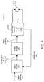
- FIG. 1 is an example diagram illustrating general components of a multi-stage amplifier device according to conventional techniques.
- amplifier 140 includes an input stage 120, a pulse width modulation stage 130, and a switched output stage 140.
- the amplifier 100 is a multi-level class D audio power amplifier.
- the amplifier 100 can be any suitable type of amplifier depending on the embodiment.
- the amplifier 140 produces an output voltage Vout to drive the load 118.
- the output voltage Vout is substantially an amplified rendition of the input voltage 105.
- the input stage 120 of the amplifier 100 receives an input signal 105.
- the input signal 105 can be received from any suitable resource such as an audio file, microphone, etc.
- the input stage 120 adjusts the input signal 105 based on feedback 145 received from the switched output stage 140.
- the switched output stage 140 includes a flying capacitor 148.
- the feedback 145 is based on a voltage stored in the flying capacitor 148 disposed in the switched output stage 140.
- the pulse width modulation stage 130 uses the adjusted input signal 125 (or signals) to produce respective pulse width modulation signals 135 that are subsequently used to drive (control) switches in the switched output stage 140.
- the switched output stage 140 generates an output voltage, Vout, to drive the load 118 (such as an audio speaker) based on states of the pulse width modulation signals 135.
- the input stage 120 produces the adjusted input signals 125 to control a magnitude of the voltage stored in the flying capacitor 148.
- modification of the received input signal 105 to adjusted input signals 125 based on the feedback 145 maintains the magnitude of the voltage across the flying capacitor 148 to a desired setpoint voltage or maintain the voltage within a desired voltage range.
- the switched output stage 140 utilizes voltage sources such as the input voltage, Pvdd, the voltage on the flying capacitor 148, and ground reference voltage to generate the output voltage, Vout.
- the adjusted input signals 125 as described herein provide control of a voltage in the flying capacitor 148 as well as provides a basis to generate Vout (such as an amplified rendition of the input signal 105) to drive the load 118.
- FIG. 2 is a more detailed example diagram illustrating implementation of a multi-stage amplifier device according to embodiments herein.
- the amplifier 100 includes audio loop filter 210, input stage 120, pulse width modulation stage 130, switched output stage 140, and load 118.
- the input stage 120 (such as implemented via analog circuitry, digital circuitry, or a combination of both analog and digital circuitry) includes input stage 120-1 and input stage 120-2.
- Input stage 120-1 includes summer 221-1, summer 221-2, gain stage 231, controllable polarity changer 241, gain stage 261 (such as "multiply by -1" amplifier (analog inverter, which is part of the controllable polarity changer 241), summer 221-3, and summer 221-4.
- Input stage 120-2 includes summer 222-1, summer 222-2, gain stage 232, controllable polarity changer 242, gain stage 262 (such as "multiply by -1" amplifier (analog inverter, which is part of controllable polarity changer 242), summer 222-3, and summer 222-4.
- Pulse width modulation stage 130 includes components as further shown and discussed in FIG. 3 .
- the switched output stage 140 includes switched output stage 140-1 (such as a first half bridge or other suitable type of switching circuit) and switched output stage 140-2 (a second half bridge or other suitable type of switching circuit).
- switched output stage 140-1 such as a first half bridge or other suitable type of switching circuit
- switched output stage 140-2 a second half bridge or other suitable type of switching circuit
- Switched output stage 140-1 includes gate drivers 141-1, switch 144-1, switch 144-2, switch 144-3, switch 144-4, flying capacitor 148-1, and comparator 151.
- the comparator 151 is an output stage current polarity detector. As shown, comparator 151 senses a representation of the instantaneous output current from source voltage Vout_a.
- Switched output stage 140-2 includes gate drivers 141-2, switch 145-1, switch 145-2, switch 145-3, switch 145-4, flying capacitor 148-2, and comparator 152.
- the comparator 152 is an output stage current polarity detector. As shown, comparator 152 senses a representation of the instantaneous output current from source voltage Vout_b.
- the audio loop filter 210 receives the input signal 205 and produces respective input signal 105 received by the input stage 120.
- the input signal 205 is an analog audio signal being amplified.
- the audio loop filter 210 can be configured to control generation of producing the input signal 105 (from input signal 205) based upon feedback such as Vout a and Vout b produced by the switched output stage 140.
- the input signal 105 is a quasi-sinusoidal analog signal offset by 750mVDC; a magnitude of the input signal 105 varies between 0 and 1.5 VDC.
- the magnitude of the input signal 105 can vary within any suitable voltage range depending on the application.
- a frequency of the input signal 105 is near DC, such as between 10 Hz and 10KHz, although the frequency can vary within any suitable range depending on the application.
- input stage 120-1 uses the input signal 105 (a.k.a., VMOD) to generate adjusted input signals 125-1 and 125-2 for phases 0 and 180.
- input signal 105 a.k.a., VMOD
- Input stage 120-1 includes an error voltage generator (such as a combination of summer 221-1 and 221-2) that compares the feedback (such as differential voltage Vcf_a_p and Vcf_a_n) from the flying capacitor 148-1 to a desired setpoint voltage of 1 ⁇ 2 Pvdd, and generates an error voltage signal EV1 indicating a difference between the magnitude of the voltage across the flying capacitor 148-1 and the desired setpoint voltage 1 ⁇ 2 Pvdd.
- an error voltage generator such as a combination of summer 221-1 and 221-2
- the feedback such as differential voltage Vcf_a_p and Vcf_a_n
- a setting of 1 ⁇ 2 Pvdd is by way of non-limiting example embodiment; the setpoint can be any suitable value.
- the summer 221-1 of the input stage 120-1 receives the differential voltage (Vcf_a_p and Vcf_a_n) across the flying capacitor 148-1.
- the summer 221-1 subtracts Vcf_a_n from Vcf_a_p to produce a difference signal Vcf1_mag (representing a magnitude of voltage across the flying capacitor 148-1).
- summer 221-2 subtracts the signal Vcf1_mag (voltage across the flying capacitor 148-1) from the desired setpoint voltage value 1 ⁇ 2 Pvdd to produce the error voltage, EV1.
- a magnitude of the error voltage, EV1 indicates an amount in which the magnitude of the voltage across the flying capacitor 148-1 is different than a desired setpoint Pvdd/2.
- Gain stage 231 of input stage 120 receives the error voltage EV1 outputted from the summer 221-2.
- Gain stage 231 applies gain (such as gain of +M) to the error voltage EV1 and inputs +M multiplied by EV1 (such as a modification value) to the controllable polarity changer 241.
- gain such as gain of +M
- +M multiplied by EV1 such as a modification value
- a magnitude of the modification value +M EV1 varies depending on a voltage across the flying capacitor 148-1.
- Comparator 151 compares a magnitude of the voltage Vout a (fed into the non-inverting input of comparator 151) to a reference value such as ground (fed into the inverting input of comparator 151) to produce control signal Iout_sign_a.
- controllable polarity changer 241 switches between inputting the gain adjusted voltage +M EV1 (+M time EV1) or -M EV1 (-M time EV1, through -1 gain stage 261 in controllable polarity changer 241) to summer 221-3 and summer 221-4.
- control signal Iout_sign_a received from switched output stage 140-1, the output of the comparator 151 (of the switched output stage 140-2) controls whether to set the output voltage MEV1 to +M EV1 or -M EV1.
- the summer 221-4 receives the input signal 105 (VMOD) and adds MEV1 (which equals +MEV1 or -MEV1 depending on a state of Iout_sign_a inputted to controllable polarity changer 241) to it.
- the summer 221-4 outputs the adjusted input signal 125-1 (such as VMOD + MEV1) to the pulse width modulation stage 130.
- Embodiments herein include sensing the output current polarity with comparator 151, and use of the sensed information to flip the feedback system polarity using controllable polarity changer 241. This is because the polarity of the output current determines the relationship between MEV1 and the flycap voltage. Note that if the current polarity is incorrect, then there would exist positive feedback in the control loop (which means that the flying capacitor voltage would become unstable) instead of negative feedback (which stabilizes the flycap voltage.)
- the summer 221-3 also receives the input signal 105 (VMOD) and subtracts MEV1 (which equals +MEV1 or -MEV1 depending on a state of Iout_sign_a) from it to produce signal 125-2.
- the summer 221-4 outputs the signal 125-2 (such as VMOD - MEV1) to the pulse width modulation stage 130 as well.
- the input stage 120-2 produces adjusted input signals 125-3 and 125-4 for different phases (such as phase 90 and 270).
- input stage 120-2 includes an error voltage generator (such as combination of summer 222-1 and 222-2) that compares the feedback (Vcf_b_p and Vcf b n) from the flying capacitor 148-2 to a desired setpoint voltage of 1 ⁇ 2 Pvdd, and generates an error voltage signal EV2 indicating a difference between the magnitude of the voltage across the flying capacitor 148-2 and the desired setpoint voltage 1 ⁇ 2 Pvdd.
- an error voltage generator such as combination of summer 222-1 and 222-2 that compares the feedback (Vcf_b_p and Vcf b n) from the flying capacitor 148-2 to a desired setpoint voltage of 1 ⁇ 2 Pvdd, and generates an error voltage signal EV2 indicating a difference between the magnitude of the voltage across the flying capacitor 148-2 and the desired setpoint voltage 1 ⁇ 2 Pvdd.
- the summer 222-1 of the input stage 120-2 receives the differential voltage (Vcf_b_p and Vcf b n) across the flying capacitor 148-2.
- the summer 221-1 subtracts Vcf_b_n from Vcf_b_p to produce a difference signal Vcf2_mag (representing a magnitude of voltage across the flying capacitor 148-2).
- summer 222-2 subtracts the signal Vcf2_mag (voltage across the flying capacitor 148-2) from the desired setpoint voltage value Pvdd/2 to produce the error voltage, EV2.
- a magnitude of the error voltage, EV2 indicates a degree to which the magnitude of the voltage across the flying capacitor 148-2 is different than a desired setpoint Pvdd/2.
- Gain stage 232 receives the error voltage EV2 outputted from the summer 222-2. Gain stage 232 applies gain (such as gain of +M) to the error voltage EV2 and inputs +M multiplied by EV2 (such as a modification value) to the controllable polarity changer 242. A magnitude of the modification value +M multiplied by EV2 varies depending on a voltage across the flying capacitor 148-2.
- Comparator 152 compares a magnitude of the voltage Vout b (fed into the non-inverting input of comparator 152) to a reference value such as ground (fed into the inverting input of comparator 152) to produce control signal Iout sign_a.
- controllable polarity changer 242 switches between inputting the gain adjusted voltage +M multiplied by EV2 or -M multiplied by EV2 (such as through -1 gain stage 262 in controllable polarity changer 242) to summer 222-3 and summer 222-4.
- control signal Iout_sign_b the output of the comparator 152 (of the switched output stage 140-2) controls whether to set the output voltage MEV2 to +M multiplied by EV2 or -M multiplied by EV2.
- the summer 222-3 receives the input signal 105 (VMOD) and adds M multiplied by EV2 (which equals +MEV2 or -MEV2 depending on a state of Iout_sign_b inputted to controllable polarity changer 242) to it.
- the summer 222-3 outputs the adjusted input signal 125-3 (such as VMOD + MEV2) to the pulse width modulation stage 130.
- Embodiments herein include sensing the output current polarity with comparator 152, and use of the sensed information to flip the feedback system polarity using controllable polarity changer 242. This is because the polarity of the output current determines the relationship between MEV2 and the flying capacitor voltage. Note that if the current polarity is incorrect, then there would exist positive feedback in the control loop (which means that the flying capacitor voltage would become unstable) instead of negative feedback (which stabilizes the flying capacitor voltage.)
- the summer 222-4 receives the input signal 105 (VMOD) and subtracts MEV2 (which equals +M multiplied by EV2 or -M multiplied by EV2 depending on a state of Iout_sign_b) from it to produce signal 125-4.
- VMOD input signal 105
- MEV2 which equals +M multiplied by EV2 or -M multiplied by EV2 depending on a state of Iout_sign_b
- the summer 222-4 outputs the signal 125-4 (such as VMOD - MEV4) to the pulse width modulation stage 130 as well.
- the input stage 120 modifies the input signal 105 (VMOD) depending on a magnitude of respective voltage stored on flying capacitor 148-1 and flying capacitor 148-2.
- FIG. 3 is an example diagram illustrating details of a pulse width modulation stage according to embodiments herein.
- the pulse width modulation stage 130 includes comparator 311, comparator 312, comparator 313, comparator 314, inverter 321, inverter 322, inverter 323, and inverter 324.
- non-inverting input (+) of the comparator 311 receives adjusted input signal 125-1 (VMOD + MEV1) generated by the input stage 120.
- the inverting input (-) of comparator 311 receives the sawtooth (or triangular) reference signal 301.
- a magnitude of the adjusted input signal 125-1 (which varies) falls within a voltage amplitude range of the sawtooth reference signal 301 (which can be any suitable range such as between 0 and 1.5VDC).
- a frequency of the sawtooth reference signal 301 is between 100 kHz and 1 MHz, although the frequency can be any suitable value.
- the comparator 311 produces a logic hi output when the magnitude of the input signal 125-1 (such as VMOD + MEV1) is greater than the magnitude of the sawtooth reference signal 301.
- the comparator 311 produces a logic lo output when the magnitude of the input signal 125-1 (such as VMOD + MEV1) is less than the magnitude of the sawtooth reference signal 301.
- the comparator 311 based on comparison of adjusted input signal 125-1 (VMOD + MEV1) to the sawtooth reference signal 301, the comparator 311 produces the pulse width modulation signal PWM0_P.
- Inverter 321 receives pulse width modulation signal PWM0_P and produces corresponding pulse width modulation signal PWM0_N, which is an inversion of the pulse width modulation signal PWM0_P.
- non-inverting input (+) of the comparator 312 receives adjusted input signal 125-2 (VMOD - MEV1) generated by the input stage 120.
- the inverting input (-) of comparator 312 receives sawtooth reference signal 302 (180 degrees apart from sawtooth reference signal 301).
- a frequency of the sawtooth reference signal 302 is between 100 kHz and 1 MHz, although the frequency can be any suitable value.
- the comparator 312 produces a logic hi output when the magnitude of the input signal 125-2 (VMOD - MEV1) is greater than the magnitude of the sawtooth reference signal 302.
- the comparator 312 produces a logic lo output when the magnitude of the input signal 125-2 (VMOD - MEV1) is less than the magnitude of the sawtooth reference signal 302.
- the comparator 312 based on comparison of adjusted input signal 125-2 (VMOD - MEV1) to the sawtooth reference signal 302, the comparator 312 produces the pulse width modulation signal PWM180_P.
- Inverter 322 receives pulse width modulation signal PWM180_P and produces corresponding pulse width modulation signal PWM180_N, which is an inversion of the pulse width modulation signal PWM180_P.
- inverting input (-) of the comparator 313 receives adjusted input signal 125-3 (VMOD + MEV2) generated by the input stage 120.
- the non-inverting input (+) of comparator 313 receives sawtooth reference signal 303 (90 degrees apart from sawtooth reference signal 301).
- a frequency of the sawtooth reference signal 301 is between 100 kHz and 1 MHz, although the frequency can be any suitable value.
- the comparator 313 produces a logic lo output when the magnitude of the input signal 125-3 (VMOD + MEV2) is greater than the magnitude of the sawtooth reference signal 303.
- the comparator 313 produces a logic hi output when the magnitude of the input signal 125-3 (VMOD + MEV2) is less than the magnitude of the sawtooth reference signal 303.
- the comparator 313 Based on comparison of adjusted input signal 125-3 (VMOD + MEV2) to the sawtooth reference signal 303, the comparator 313 produces the pulse width modulation signal PWM90_P.
- Inverter 323 receives pulse width modulation signal PWM90_P and produces corresponding pulse width modulation signal PWM90_N, which is an inversion of the pulse width modulation signal PWM90_P.
- inverting input (-) of the comparator 314 receives adjusted input signal 125-4 (VMOD - MEV2) generated by the input stage 120.
- the non-inverting input (+) of comparator 314 receives sawtooth reference signal 304 (270 degrees apart from sawtooth reference signal 301).
- a frequency of the sawtooth reference signal 301 is between 100 kHz and 1 MHz, although the frequency can be any suitable value.
- the comparator 314 produces a logic lo output when the magnitude of the input signal 125-4 (VMOD - MEV2) is greater than the magnitude of the sawtooth reference signal 304.
- the comparator 314 produces a logic hi output when the magnitude of the input signal 125-4 (VMOD - MEV2) is less than the magnitude of the sawtooth reference signal 304.
- the comparator 314 based on comparison of adjusted input signal 125-4 (VMOD - MEV2) to the sawtooth reference signal 304, the comparator 314 produces the pulse width modulation signal PWM270_N.
- Inverter 324 receives pulse width modulation signal PWM270_P and produces corresponding pulse width modulation signal PWM270_N, which is an inversion of the pulse width modulation signal PWM270_P.
- a frequency ( f sw ) of the pulse width modulation signals is between 100 and 200 KHz, although the frequency can be any suitable value.
- the switched output stage 140-1 includes a sequence of series connected switches (such as one or more half bridge-type circuits including respective switches) to drive Vout_a or Vout_b to the load 118.
- the pulse width modulation control signals as previously discussed control states of the switches 144.
- the flying capacitor 148-1 is coupled to the series connected switches 144 in switched output stage 140-1; flying capacitor 148-2 is coupled to switches 145 in the switched output stage 140-2.
- the input stage 120 produces one or more adjusted input signals 125 to control a magnitude of the voltage stored in the flying capacitors 148.
- modification of the received input signal 105 based on the feedback of the voltage of the flying capacitors 148 and generation of the adjusted input signals 125 maintains the magnitude of the voltage across each of the flying capacitors 148-1 and 148-2 to a desired setpoint voltage (such as 1 ⁇ 2 Pvdd).
- the input signal 105 being amplified can be modified such that the modified input signals 125 control a magnitude of voltage on the flying capacitors 148 as well as control switches to produce the output voltage Vout a and Vout b (replica of input signal 105).
- a logic hi voltage of a respective pulse width modulation signal activates a respective switch while a logic low deactivates a respective switch.
- the pulse width modulation signal PWM0_P drives the gate of switch 144-1 (such as a field effect transistor or other suitable switch component) to control activation of switch 144-1;
- the pulse width modulation signal PWM180_P drives the gate of switch 144-2 (such as a field effect transistor or other suitable switch component) to control activation of switch 144-2;
- the pulse width modulation signal PWM180_N drives the gate of switch 144-3 (such as a field effect transistor or other suitable switch component) to control activation of switch 144-3;
- the pulse width modulation signal PWM0_N drives the gate of switch 144-4 (such as a field effect transistor or other suitable switch component) to control activation of switch 144-4.
- the pulse width modulation signal PWM90_N drives the gate of switch 145-1 (such as a field effect transistor or other suitable switch component) to control activation of switch 145-1;
- the pulse width modulation signal PWM270_N drives the gate of switch 145-2 (such as a field effect transistor or other suitable switch component) to control activation of switch 145-2;
- the pulse width modulation signal PWM270_P drives the gate of switch 145-3 (such as a field effect transistor or other suitable switch component) to control activation of switch 145-3;
- the pulse width modulation signal PWM90_P drives the gate of switch 145-4 (such as a field effect transistor or other suitable switch component) to control activation of switch 145-4.
- the input stage 120 receives an input signal 105 such as an audio signal.
- the input stage 120 applies adjustments to the input signal 105 based on feedback (such as Vcf_a_p and Vcf_a_n from flying capacitor 148-1 and Vcf_b_p and Vcf_b_n from flying capacitor 148-2) from the switched output stage 140.
- the pulse width modulation stage 130 uses the adjusted input signals 125 to produce respective pulse width modulation signals 135 that are subsequently used to drive (control) switches 144 and 145) in the switched output stage 140.
- the switched output stage 140 generates an output voltage Vout_a and Vout_b to drive a load 119 (such as an audio speaker, modeled as an inductor, or voice coil, in series with and resistor) based on states of the pulse width modulation signals 135.
- a load 119 such as an audio speaker, modeled as an inductor, or voice coil, in series with and resistor
- the output voltage Vout is an amplified rendition of the input signal 105.
- embodiments herein are useful over conventional techniques of implementing and controlling a flying capacitor voltage.
- the novel flying capacitor voltage control techniques as described herein provide smoother and less noisy operation of an amplifier 100, making it possible to implement smaller flying capacitors in amplifier 100.
- analog or digital circuitry calculates a deviation of a flying capacitor voltage an ideal value such as 1 ⁇ 2Pvdd (rail voltage to power the amplifier and switched output stage 140).
- an input stage 120 generates an error voltage
- one embodiment herein includes continuously (or on cycle-by-cycle basis, which is effectively the same) alter PWM (Pulse Width Modulation) duty cycles between switch pairs in a flying capacitor half bridge circuit to control the flying capacitor voltage.
- PWM Pulse Width Modulation
- Such embodiments provide a compact and low-noise solution to flying capacitor voltage balancing, ensuring that the best idle power (due to multi-level at low switching frequency) and audio performance (due to minimum flying capacitor balancing noise, even at low switching frequency) are simultaneously achievable.
- the amplifier 100 supports four phases (namely, phases 0, 90, 180, and 270). Note that the amplifier 100 as described herein can be configured to support any number of N phases via suitable circuitry.
- FIG. 4 is an example diagram illustrating control and operation of a switched output stage according to embodiments herein.
- the switched output stage 140-1 includes switch 144-1, switch 144-2, switch 144-3, and switch 144-4.
- a logic hi applied to a respective gate of a switch controls a state of the respective switch to an ON state (low resistance path);
- a logic lo applied to a respective gate of a switch controls a state of the respective switch to an OFF state (high resistance path).
- the pulse width modulation signal PWM0_P controls switch 144-1; the pulse width modulation signal PWM0_N controls switch 144-4.
- the pulse width modulation signal PWM180_P controls switch 144-2; the pulse width modulation signal PWM180_N controls switch 144-3.
- pulse width modulation signal PWM90_N controls switch 145-1; the pulse width modulation signal PWM90_P controls switch 145-4.
- the pulse width modulation signal PWM270_N controls switch 145-2; the pulse width modulation signal PWM270_P controls switch 145-3.
- FIG. 5 is an example diagram illustrating different operational modes of a switched output stage according to embodiments herein.
- the different possible modes in which to control the switches 144-1, 144-2, 144-3, and 144-4 includes mode A, mode B, mode C, and mode D.
- flying capacitor 148-1 stores a voltage 1 ⁇ 2 Pvdd. Accordingly, the switched output stage 140 can be configured to output voltages Pvdd, 1 ⁇ 2 Pvdd, or 0 VDC depending on a state of the respective switches 144-1, 144-2, 144-3, and 144-4.
- the pulse width modulation signal PWM0_P drives the gate of switch 144-1 such that switch 144-1 is ON;
- the pulse width modulation signal PWM180_P drives the gate of switch 144-2 such that switch 144-2 is ON;
- the pulse width modulation signal PWM180_N drives the gate of switch 144-3 such that switch 144-3 is OFF, the switch 140-3 effectively becomes inherent diode 140-D3;
- the pulse width modulation signal PWM0_N drives the gate of switch 144-4 such that switch 144-4 is OFF, the switch 144-4 effectively becomes inherent diode 144-D4.
- the output voltage Vouta is approximately equal to voltage Pvdd.
- the pulse width modulation signal PWM0_P drives the gate of switch 144-1 such that switch 144-1 is ON;
- the pulse width modulation signal PWM180_P drives the gate of switch 144-2 such that switch 144-2 is OFF, the switch 144-2 effectively becomes inherent diode 140-D2;
- the pulse width modulation signal PWM180_N drives the gate of switch 144-3 such that switch 144-3 is ON;
- the pulse width modulation signal PWM0_N drives the gate of switch 144-4 such that switch 144-4 is OFF, the switch 144-4 effectively becomes inherent diode 144-D4.
- the output voltage Vouta from the switched output stage 140-1 is approximately equal to voltage 1 ⁇ 2 Pvdd.
- the pulse width modulation signal PWM0_P drives the gate of switch 144-1 such that switch 144-1 is OFF, the switch 144-1 effectively becomes inherent diode 144-D1;
- the pulse width modulation signal PWM180_P drives the gate of switch 144-2 such that switch 144-2 is ON;
- the pulse width modulation signal PWM180_N drives the gate of switch 144-3 such that switch 144-3 is OFF, the switch 144-3 effectively becomes inherent diode 144-D3;
- the pulse width modulation signal PWM0_N drives the gate of switch 144-4 such that switch 144-4 is ON.
- the output voltage Vouta is approximately equal to voltage 1 ⁇ 2 Pvdd.
- the pulse width modulation signal PWM0_P drives the gate of switch 144-1 such that switch 140-1 is OFF, the switch 144-1 effectively becomes inherent diode 144-D1;
- the pulse width modulation signal PWM180_P drives the gate of switch 144-2 such that switch 144-2 is OFF, the switch 144-2 effectively becomes inherent diode 144-D2;
- the pulse width modulation signal PWM180_N drives the gate of switch 144-3 such that switch 144-3 is ON;
- the pulse width modulation signal PWM0_N drives the gate of switch 144-4 such that switch 144-4 is ON.
- the output voltage Vouta is approximately equal to voltage 0 VDC.
- the pulse width modulation stage 130 controls group of switches 145 in the switched output stage 140-2 in a similar manner based on 90 and 270 phase pulse width modulation control signals to output different voltage levels associated with voltage Voutb.
- FIG. 6 is an example diagram illustrating generation of a modulated output signal according to embodiments herein.
- the pulse width modulation stage 130 drives the switched output stage 140 using pulse width modulation signals as previously discussed.
- the voltage across the load 118 is Vouta - Voutb (differential signal or modulated signal).
- the load 118 includes a filter (such as a series connected resistor and inductor) to smooth the modulated signal Vouta-Voutb into an amplified replica of the input signal 105 (such as a sine-wave, quasi-sine wave, variable voltage signal, etc.).
- a filter such as a series connected resistor and inductor to smooth the modulated signal Vouta-Voutb into an amplified replica of the input signal 105 (such as a sine-wave, quasi-sine wave, variable voltage signal, etc.).
- FIG. 7 is a flowchart 700 illustrating an example method according to embodiments herein. Note that there will be some overlap with respect to concepts as discussed above.
- the input stage 120 receives an input signal 105 (such as an audio signal) to be played back over a load 118 such as a speaker.
- an input signal 105 such as an audio signal
- the input stage 120 applies modifications (based on error voltage, EV x ) to the input signal 105 based on feedback 145 associated with a flying capacitor 148, namely Cfly, in the switched output stage 140 of the amplifier 100 driving load 118.
- the modifications to the input signal 105 control the magnitude of the voltage on the flying capacitor 148, Cfly.
- the pulse width modulation stage 130 produces pulse width modulation signals 135 from the adjusted input signals 125.
- the switched output stage 140 at least occasionally uses the voltage on the flying capacitor 148 (Cfly) to drive the load 118 with an output voltage (such as Vout a).
- the switched output stage 140 provides feedback 145 from the flying capacitor 148 (Cfly) to the input stage 120.
- a method includes: receiving an input signal; applying modifications to the input signal based on feedback from a switched output stage of an amplifier driving a load to generate an adjusted input signal; producing pulse width modulation signals from the adjusted input signal; and driving the load with an output voltage based on the pulse width modulation signals.
- the method further includes: adjusting the input signal depending upon a magnitude of a voltage stored in a flying capacitor of the switched output stage driving the load.
- the flying capacitor stores an intermediate voltage to power the load, wherein a magnitude of the intermediate voltage is a predetermined fraction of a magnitude of a power rail powering the switched output stage.
- applying modifications includes: producing a modification value based on the feedback; producing multiple adjusted input signals using the modification value; and via the multiple just input signals, controlling a magnitude of a voltage stored in a flying capacitor of the switched output stage.
- applying the modifications to the input signal includes: individually deriving a respective adjusted input signal for each of multiple phases in the switched output stage using the feedback; and utilizing the respective adjusted input signals to produce pulse width modulation signals to drive the phases in the switched output stage.
- modifying the input signal includes: comparing the feedback to a desired setpoint voltage, the feedback indicating a magnitude of a voltage across a flying capacitor disposed in the switched output stage; generate an error voltage signal indicating a difference between the magnitude of the voltage across the flying capacitor and the desired setpoint voltage; and producing the adjusted input signal by modifying the received input signal based on the error voltage signal.
- the method further includes: via the adjusted input signal, maintaining the magnitude of the voltage across the flying capacitor to the desired setpoint voltage.
- the input signal is an audio signal
- the output signal being an amplified rendition of the input signal
- driving the load with the output voltage based on the pulse width modulation signals includes: driving the load with a differential output voltage, the differential output voltage including a first output voltage generated by a first half bridge circuit and a second output voltage generated by a second half bridge circuit; wherein applying the modifications to the input signal based on the feedback includes: i) receiving first feedback from a first flying capacitor coupled to the first half bridge circuit, ii) receiving second feedback from a second flying capacitor coupled to the second half bridge circuit, and iii) applying adjustments to the input signal to maintain a voltage across the first flying capacitor and maintain a voltage across the second flying capacitor at a desired setpoint.
- applying the modifications to the input signal based on the feedback includes: deriving multiple adjusted input signals from the input signal based on the feedback.
- the method further includes: converting the adjusted input signals into the pulse width modulation signals.
- applying modifications to the input signal includes: producing a modification value based on the feedback; summing the received input signal and the modification value to produce a first adjusted input signal; subtracting the modification value from the received input signal to produce a second adjusted input signal, the first adjusted input signal and the second adjusted input signal being a complementary adjustment signal pair; and via the complementary adjustment signal pair, controlling a corresponding set of series connected transistors in the switched output stage driving the load.
Landscapes
- Engineering & Computer Science (AREA)
- Power Engineering (AREA)
- Multimedia (AREA)
- Amplifiers (AREA)
Abstract
Description
- Conventional audio amplifiers sometimes include a so-called flying capacitor disposed in a respective switched output stage to drive a load. Typically, the flying capacitor stores an intermediate voltage value whose magnitude is a fraction of a magnitude of a main voltage rail powering the switched output stage. Presence of the flying capacitor enables a controller to apply the voltage of the flying capacitor to a load in addition to being able to apply standard voltage rails such as main power source voltage and ground to the load.
- As a more specific example, a main voltage rail of a switched output stage of an amplifier may be 5 volts DC; the voltage on the flying capacitor may be set to ½ the main voltage rail or 2.5 volts DC. When present in an amplifier circuit, the so-called flying capacitor is electrically coupled across multiple switches in a switched output stage (such a sequence of series connected switches configured as a bridge circuit).
- As is known, the switches in the switched output stage can be independently controlled to produce an output voltage to drive the load. For example, the switches in the output stage can be controlled (switched ON and OFF at appropriate time) to drive the load with a maximum voltage (main voltage rail) or ground reference voltage at different times.
- As mentioned, in addition to having an ability to drive a load with a main voltage rail or a ground reference value, presence of one or more the flying capacitors in a respective drive circuit enables the output stage to drive the load with voltages of the one or more flying capacitors at different times. Thus, via activation of different combination of switches in the switched output stage, a respective controller is able to software between driving a load with voltages of different voltage magnitudes such as a main rail voltage, one or more intermediate or fractional voltages (stored in the one or more flying capacitors), and a ground reference voltage to produce an output voltage to power a respective load.
- Ideally, a voltage stored in a flying capacitor is precisely maintained at a predetermined value. This ensures accurate generation of an output voltage. However, one drawback of the conventional implementation of a flying capacitor in an amplifier circuit is that the voltage across the flying capacitor can drift or vary with respect to a desired setpoint value. In such an instance, undesirable variations in the intermediate voltage stored in the flying capacitor (that is used to drive a respective load) results in unwanted noise or distortion in a generated output signal.
- Embodiments herein include novel ways of providing improved performance of an amplifier and generation of an output voltage.
- For example, according to one embodiment, an amplifier includes: an input stage, a pulse width modulation stage, and a switched output stage. During operation, the input stage receives an input signal such as an audio signal. The input stage adjusts the input signal based on feedback from the switched output stage. In one embodiment, the feedback is associated with the flying capacitor disposed in the switched output stage. The pulse width modulation stage uses the adjusted input signal or input signals to produce respective pulse width modulation signals that are subsequently used to drive (control) switches in the switched output stage. The switched output stage then generates an output voltage to drive a load (such as an audio speaker) based on states of the pulse width modulation signals. Typically, the output voltage driving the load is an amplified rendition of the input signal.
- In one embodiment, the switched output stage includes a sequence of series connected switches (such as one or more bridge-type circuits) to drive the load; the flying capacitor is coupled to the series connected switches. Further, the input stage produces one or more adjusted input signals to control a magnitude of the voltage stored in the flying capacitor. In other words, in one embodiment, generation of the one or more adjusted input signals based on the feedback from the flying capacitor maintains the magnitude of the voltage across the flying capacitor to a desired setpoint voltage. Thus, the input signal being amplified to drive a load can be modified such that the modified input signal also controls a magnitude of voltage on respective one or more flying capacitors.
- In still further embodiments, the feedback from the output stage is a magnitude of a voltage of the flying capacitor in the switched output stage. In such an instance, the input stage adjusts the input signal based on a magnitude of the voltage stored in the flying capacitor of the switched output stage. As previously discussed, the adjustments to the input signal maintain the voltage on the flying capacitor at a desired setpoint (such as half, one third, etc.) of a magnitude of a voltage rail powering the output stage.
- By further way of nonlimiting example, the flying capacitor stores an intermediate voltage to power the load; the intermediate voltage has a magnitude that is a predetermined percentage or amount of the voltage rail powering the output stage. In one non-limiting example embodiment, a primary voltage rail powering the switched output stage is Pvdd; via the adjusted input signals, the voltage of the flying capacitor is controlled to be ½ Vppd. Note that the desired magnitude of the flying capacitor voltage and setpoint can vary depending on the embodiment.
- Note further that the input stage of the amplifier as described herein can be configured to produce a modification value (such as an error voltage itself or gain adjusted error voltage value) based on the received feedback. In such an embodiment, the input stage produces one or more adjusted input signals using the modification value to control a magnitude of a voltage stored in a flying capacitor of the switched output stage.
- More specifically, in one embodiment, the input stage can be configured to include: an error voltage generator operable to: i) compare the feedback from the flying capacitor to a desired setpoint voltage, and ii) generate an error voltage signal indicating a difference between the magnitude of the voltage across the flying capacitor and the desired setpoint voltage.
- The input stage can further include an adjustor. In one embodiment, the adjustor in the input stage modifies the received input signal based on a magnitude of the generated error voltage signal produced by the error voltage generator. For example, for a first phase of multiple phases, the adjustor in the input stage produces a first adjustment signal based on summing the input signal and the modification value (such as the error voltage or a gain adjusted error voltage); for a second phase of the multiple phases, the adjustor produces a second adjustment signal based on subtracting the modification value from the received input signal.
- In one nonlimiting example embodiment, the multiple adjusted input signals (such as the first adjustment signal and the second adjustments signal) represent a complementary signal pair that is generated to control a corresponding first phase and second phase of multiple phases supported in the amplifier to produce the output voltage driving the load.
- The adjusted input signals can be analog or digital signals.
- Note that the pulse width modulation stage can be a multi-phase pulse width modulation signal generator operable to drive N-phases/switch pairs in the switched output stage. More specifically, in a manner as previously discussed, the input stage is operable to individually derive (produce) a respective adjusted input signal for each of the N-phases of the amplifier using received feedback from one or more flying capacitors present in the switched output stage. In one embodiment, each of the adjusted input signals generated by the input stage controls a corresponding phase or pair of complementary switches in the output stage driving the load.
- Embodiments herein are useful over conventional techniques of controlling a flying capacitor voltage. For example, embodiments herein include novel flying capacitor voltage control techniques that result in producing a smoother and less noisy output voltage, making it possible to implement smaller flying capacitors in a respective amplifier application. In one embodiment, as described herein, analog or digital circuitry calculates a deviation of a flying capacitor voltage with respect to an ideal value such as ½Pvdd (rail voltage to power the amplifier). Further, as previously discussed, an input stage of the amplifier generates an error voltage, which is used as a basis to modify the duty cycles of the individual switch pairs in a multi-level half bridge circuit. Adjustments to the duty cycles control an average flying capacitor current to a desired value.
- As further described herein, one embodiment herein includes continuously (or on cycle-by-cycle basis, which is effectively the same) alter PWM (Pulse Width Modulation) duty cycles amongst switch pairs in a half bridge circuit to control a respective flying capacitor voltage in the half bridge circuit. Such embodiments provide a compact and low-noise solution to flying capacitor voltage balancing, ensuring that the best idle power (due to multi-level at low switching frequency) and audio performance (due to minimum flying capacitor balancing noise, even at low switching frequency) are simultaneously achievable.
- These and other more specific embodiments are disclosed in more detail below.
- Note further that although embodiments as discussed herein are applicable to amplifier circuitry, the concepts disclosed herein may be advantageously applied to any other suitable topologies.
- Note that although each of the different features, techniques, configurations, etc., herein may be discussed in different places of this disclosure, it is intended, where appropriate, that each of the concepts can optionally be executed independently of each other or in combination with each other. Accordingly, the one or more present inventions as described herein can be embodied and viewed in many different ways.
- Also, note that this preliminary discussion of embodiments herein purposefully does not specify every embodiment and/or incrementally novel aspect of the present disclosure or claimed invention(s). Instead, this brief description only presents general embodiments and corresponding points of novelty over conventional techniques. For additional details and/or possible perspectives (permutations) of the invention(s), the reader is directed to the Detailed Description section and corresponding figures of the present disclosure as further discussed below.
-
FIG. 1 is an example diagram illustrating components of an amplifier device according to conventional techniques. -
FIG. 2 is a more detailed example diagram illustrating implementation of an amplifier device according to embodiments herein. -
FIG. 3 is an example diagram illustrating details of a pulse width modulation stage according to embodiments herein. -
FIG. 4 is an example diagram illustrating control and operation of a switched output stage according to embodiments herein. -
FIG. 5 is an example diagram illustrating different operational modes of a switched output stage according to embodiments herein. -
FIG. 6 is an example diagram illustrating generation of a modulated output signal according to embodiments herein. -
FIG. 7 is an example diagram illustrating a method of providing signal generation according to embodiments herein. - The foregoing and other objects, features, and advantages of embodiments herein will be apparent from the following more particular description herein, as illustrated in the accompanying drawings in which like reference characters refer to the same parts throughout the different views. The drawings are not necessarily to scale, with emphasis instead being placed upon illustrating the embodiments, principles, concepts, etc.
- According to one embodiment, an amplifier includes: an input stage, a pulse width modulation stage, and a switched output stage. The input stage receives an input signal. The input stage adjusts the input signal based on feedback from the switched output stage that drives a load. In one embodiment, the feedback indicates a voltage across a flying capacitor in the switched output stage. The pulse width modulation stage uses the adjusted input signal or signals to produce respective pulse width modulation signals that are subsequently used to drive (control) switches in the switched output stage, resulting in generation of an output voltage to power the load. In one embodiment, the output voltage is a substantial replica of the input signal. Repeated or continuous adjustments (such as cycle after cycle) to the input signal maintain the voltage on the flying capacitor at a desired service provider value (or within a desired voltage range).
-
FIG. 1 is an example diagram illustrating general components of a multi-stage amplifier device according to conventional techniques. - As shown in this example embodiment,
amplifier 140 includes aninput stage 120, a pulsewidth modulation stage 130, and a switchedoutput stage 140. - In one embodiment, the
amplifier 100 is a multi-level class D audio power amplifier. However, note that theamplifier 100 can be any suitable type of amplifier depending on the embodiment. - In general, the
amplifier 140 produces an output voltage Vout to drive theload 118. The output voltage Vout is substantially an amplified rendition of theinput voltage 105. - As shown in
FIG. 1 , theinput stage 120 of theamplifier 100 receives aninput signal 105. Theinput signal 105 can be received from any suitable resource such as an audio file, microphone, etc. - In furtherance of producing the output voltage, Vout, the
input stage 120 adjusts theinput signal 105 based onfeedback 145 received from the switchedoutput stage 140. In one embodiment, the switchedoutput stage 140 includes a flyingcapacitor 148. Thefeedback 145 is based on a voltage stored in the flyingcapacitor 148 disposed in the switchedoutput stage 140. - The pulse
width modulation stage 130 uses the adjusted input signal 125 (or signals) to produce respective pulse width modulation signals 135 that are subsequently used to drive (control) switches in the switchedoutput stage 140. The switchedoutput stage 140 generates an output voltage, Vout, to drive the load 118 (such as an audio speaker) based on states of the pulse width modulation signals 135. - In one embodiment, the
input stage 120 produces the adjusted input signals 125 to control a magnitude of the voltage stored in the flyingcapacitor 148. In other words, modification of the receivedinput signal 105 to adjusted input signals 125 based on thefeedback 145 maintains the magnitude of the voltage across the flyingcapacitor 148 to a desired setpoint voltage or maintain the voltage within a desired voltage range. As further discussed below, the switchedoutput stage 140 utilizes voltage sources such as the input voltage, Pvdd, the voltage on the flyingcapacitor 148, and ground reference voltage to generate the output voltage, Vout. - Accordingly, in contrast to conventional techniques, the adjusted input signals 125 as described herein provide control of a voltage in the flying
capacitor 148 as well as provides a basis to generate Vout (such as an amplified rendition of the input signal 105) to drive theload 118. -
FIG. 2 is a more detailed example diagram illustrating implementation of a multi-stage amplifier device according to embodiments herein. - As shown in
FIG. 2 , theamplifier 100 includesaudio loop filter 210,input stage 120, pulsewidth modulation stage 130, switchedoutput stage 140, andload 118. - As further shown, the input stage 120 (such as implemented via analog circuitry, digital circuitry, or a combination of both analog and digital circuitry) includes input stage 120-1 and input stage 120-2.
- Input stage 120-1 includes summer 221-1, summer 221-2, gain
stage 231,controllable polarity changer 241, gain stage 261 (such as "multiply by -1" amplifier (analog inverter, which is part of the controllable polarity changer 241), summer 221-3, and summer 221-4. - Input stage 120-2 includes summer 222-1, summer 222-2, gain
stage 232, controllable polarity changer 242, gain stage 262 (such as "multiply by -1" amplifier (analog inverter, which is part of controllable polarity changer 242), summer 222-3, and summer 222-4. - Pulse
width modulation stage 130 includes components as further shown and discussed inFIG. 3 . - Referring again to
FIG. 2 , the switchedoutput stage 140 includes switched output stage 140-1 (such as a first half bridge or other suitable type of switching circuit) and switched output stage 140-2 (a second half bridge or other suitable type of switching circuit). - Switched output stage 140-1 includes gate drivers 141-1, switch 144-1, switch 144-2, switch 144-3, switch 144-4, flying capacitor 148-1, and
comparator 151. - In one embodiment, the
comparator 151 is an output stage current polarity detector. As shown,comparator 151 senses a representation of the instantaneous output current from source voltage Vout_a. - Switched output stage 140-2 includes gate drivers 141-2, switch 145-1, switch 145-2, switch 145-3, switch 145-4, flying capacitor 148-2, and
comparator 152. - In one embodiment, the
comparator 152 is an output stage current polarity detector. As shown,comparator 152 senses a representation of the instantaneous output current from source voltage Vout_b. - During operation, the
audio loop filter 210 receives theinput signal 205 and producesrespective input signal 105 received by theinput stage 120. In one embodiment, theinput signal 205 is an analog audio signal being amplified. - The
audio loop filter 210 can be configured to control generation of producing the input signal 105 (from input signal 205) based upon feedback such as Vout a and Vout b produced by the switchedoutput stage 140. - In one non-limiting example embodiment, the
input signal 105 is a quasi-sinusoidal analog signal offset by 750mVDC; a magnitude of theinput signal 105 varies between 0 and 1.5 VDC. However, note that the magnitude of theinput signal 105 can vary within any suitable voltage range depending on the application. - In one embodiment, a frequency of the
input signal 105 is near DC, such as between 10 Hz and 10KHz, although the frequency can vary within any suitable range depending on the application. - As further shown, input stage 120-1 uses the input signal 105 (a.k.a., VMOD) to generate adjusted input signals 125-1 and 125-2 for
phases 0 and 180. - Input stage 120-1 includes an error voltage generator (such as a combination of summer 221-1 and 221-2) that compares the feedback (such as differential voltage Vcf_a_p and Vcf_a_n) from the flying capacitor 148-1 to a desired setpoint voltage of ½ Pvdd, and generates an error voltage signal EV1 indicating a difference between the magnitude of the voltage across the flying capacitor 148-1 and the desired setpoint voltage ½ Pvdd.
- Note again that a setting of ½ Pvdd is by way of non-limiting example embodiment; the setpoint can be any suitable value.
- More specifically, via a feedback path from the switched
output stage 140 to theinput stage 120, the summer 221-1 of the input stage 120-1 receives the differential voltage (Vcf_a_p and Vcf_a_n) across the flying capacitor 148-1. - The summer 221-1 subtracts Vcf_a_n from Vcf_a_p to produce a difference signal Vcf1_mag (representing a magnitude of voltage across the flying capacitor 148-1).
- As further shown, summer 221-2 subtracts the signal Vcf1_mag (voltage across the flying capacitor 148-1) from the desired setpoint voltage value ½ Pvdd to produce the error voltage, EV1. A magnitude of the error voltage, EV1, indicates an amount in which the magnitude of the voltage across the flying capacitor 148-1 is different than a desired setpoint Pvdd/2.
-
Gain stage 231 ofinput stage 120 receives the error voltage EV1 outputted from the summer 221-2.Gain stage 231 applies gain (such as gain of +M) to the error voltage EV1 and inputs +M multiplied by EV1 (such as a modification value) to thecontrollable polarity changer 241. In a manner as previously discussed, a magnitude of the modification value +M EV1 varies depending on a voltage across the flying capacitor 148-1. -
Comparator 151 compares a magnitude of the voltage Vout a (fed into the non-inverting input of comparator 151) to a reference value such as ground (fed into the inverting input of comparator 151) to produce control signal Iout_sign_a. - Based on control signal Iout_sign_a,
controllable polarity changer 241 switches between inputting the gain adjusted voltage +M EV1 (+M time EV1) or -M EV1 (-M time EV1, through -1gain stage 261 in controllable polarity changer 241) to summer 221-3 and summer 221-4. Thus, via control signal Iout_sign_a received from switched output stage 140-1, the output of the comparator 151 (of the switched output stage 140-2) controls whether to set the output voltage MEV1 to +M EV1 or -M EV1. - As further shown, the summer 221-4 (such as an adjustor) receives the input signal 105 (VMOD) and adds MEV1 (which equals +MEV1 or -MEV1 depending on a state of Iout_sign_a inputted to controllable polarity changer 241) to it. In this example embodiment, the summer 221-4 outputs the adjusted input signal 125-1 (such as VMOD + MEV1) to the pulse
width modulation stage 130. - Embodiments herein include sensing the output current polarity with
comparator 151, and use of the sensed information to flip the feedback system polarity usingcontrollable polarity changer 241. This is because the polarity of the output current determines the relationship between MEV1 and the flycap voltage. Note that if the current polarity is incorrect, then there would exist positive feedback in the control loop (which means that the flying capacitor voltage would become unstable) instead of negative feedback (which stabilizes the flycap voltage.) - The summer 221-3 also receives the input signal 105 (VMOD) and subtracts MEV1 (which equals +MEV1 or -MEV1 depending on a state of Iout_sign_a) from it to produce signal 125-2. The summer 221-4 outputs the signal 125-2 (such as VMOD - MEV1) to the pulse
width modulation stage 130 as well. - In a similar manner, the input stage 120-2 produces adjusted input signals 125-3 and 125-4 for different phases (such as phase 90 and 270).
- For example, input stage 120-2 includes an error voltage generator (such as combination of summer 222-1 and 222-2) that compares the feedback (Vcf_b_p and Vcf b n) from the flying capacitor 148-2 to a desired setpoint voltage of ½ Pvdd, and generates an error voltage signal EV2 indicating a difference between the magnitude of the voltage across the flying capacitor 148-2 and the desired setpoint voltage ½ Pvdd.
- More specifically, as shown, the summer 222-1 of the input stage 120-2 receives the differential voltage (Vcf_b_p and Vcf b n) across the flying capacitor 148-2.
- The summer 221-1 subtracts Vcf_b_n from Vcf_b_p to produce a difference signal Vcf2_mag (representing a magnitude of voltage across the flying capacitor 148-2).
- As further shown, summer 222-2 subtracts the signal Vcf2_mag (voltage across the flying capacitor 148-2) from the desired setpoint voltage value Pvdd/2 to produce the error voltage, EV2. A magnitude of the error voltage, EV2, indicates a degree to which the magnitude of the voltage across the flying capacitor 148-2 is different than a desired setpoint Pvdd/2.
-
Gain stage 232 receives the error voltage EV2 outputted from the summer 222-2.Gain stage 232 applies gain (such as gain of +M) to the error voltage EV2 and inputs +M multiplied by EV2 (such as a modification value) to the controllable polarity changer 242. A magnitude of the modification value +M multiplied by EV2 varies depending on a voltage across the flying capacitor 148-2. -
Comparator 152 compares a magnitude of the voltage Vout b (fed into the non-inverting input of comparator 152) to a reference value such as ground (fed into the inverting input of comparator 152) to produce control signal Iout sign_a. - Based on control signal Iout_sign_b, controllable polarity changer 242 switches between inputting the gain adjusted voltage +M multiplied by EV2 or -M multiplied by EV2 (such as through -1
gain stage 262 in controllable polarity changer 242) to summer 222-3 and summer 222-4. - Thus, via control signal Iout_sign_b, the output of the comparator 152 (of the switched output stage 140-2) controls whether to set the output voltage MEV2 to +M multiplied by EV2 or -M multiplied by EV2.
- As further shown, the summer 222-3 (such as an adjustor) receives the input signal 105 (VMOD) and adds M multiplied by EV2 (which equals +MEV2 or -MEV2 depending on a state of Iout_sign_b inputted to controllable polarity changer 242) to it. The summer 222-3 outputs the adjusted input signal 125-3 (such as VMOD + MEV2) to the pulse
width modulation stage 130. - Embodiments herein include sensing the output current polarity with
comparator 152, and use of the sensed information to flip the feedback system polarity using controllable polarity changer 242. This is because the polarity of the output current determines the relationship between MEV2 and the flying capacitor voltage. Note that if the current polarity is incorrect, then there would exist positive feedback in the control loop (which means that the flying capacitor voltage would become unstable) instead of negative feedback (which stabilizes the flying capacitor voltage.) - The summer 222-4 receives the input signal 105 (VMOD) and subtracts MEV2 (which equals +M multiplied by EV2 or -M multiplied by EV2 depending on a state of Iout_sign_b) from it to produce signal 125-4.
- The summer 222-4 outputs the signal 125-4 (such as VMOD - MEV4) to the pulse
width modulation stage 130 as well. - Accordingly, the
input stage 120 modifies the input signal 105 (VMOD) depending on a magnitude of respective voltage stored on flying capacitor 148-1 and flying capacitor 148-2. -
FIG. 3 is an example diagram illustrating details of a pulse width modulation stage according to embodiments herein. - As shown in this example embodiment, the pulse
width modulation stage 130 includescomparator 311,comparator 312,comparator 313,comparator 314,inverter 321,inverter 322,inverter 323, andinverter 324. - As shown, non-inverting input (+) of the
comparator 311 receives adjusted input signal 125-1 (VMOD + MEV1) generated by theinput stage 120. The inverting input (-) ofcomparator 311 receives the sawtooth (or triangular)reference signal 301. In one embodiment, a magnitude of the adjusted input signal 125-1 (which varies) falls within a voltage amplitude range of the sawtooth reference signal 301 (which can be any suitable range such as between 0 and 1.5VDC). Typically, a frequency of thesawtooth reference signal 301 is between 100 kHz and 1 MHz, although the frequency can be any suitable value. - In this example embodiment, the
comparator 311 produces a logic hi output when the magnitude of the input signal 125-1 (such as VMOD + MEV1) is greater than the magnitude of thesawtooth reference signal 301. Thecomparator 311 produces a logic lo output when the magnitude of the input signal 125-1 (such as VMOD + MEV1) is less than the magnitude of thesawtooth reference signal 301. - In this example embodiment, based on comparison of adjusted input signal 125-1 (VMOD + MEV1) to the
sawtooth reference signal 301, thecomparator 311 produces the pulse width modulation signal PWM0_P. -
Inverter 321 receives pulse width modulation signal PWM0_P and produces corresponding pulse width modulation signal PWM0_N, which is an inversion of the pulse width modulation signal PWM0_P. - As further shown, non-inverting input (+) of the
comparator 312 receives adjusted input signal 125-2 (VMOD - MEV1) generated by theinput stage 120. The inverting input (-) ofcomparator 312 receives sawtooth reference signal 302 (180 degrees apart from sawtooth reference signal 301). Typically, a frequency of thesawtooth reference signal 302 is between 100 kHz and 1 MHz, although the frequency can be any suitable value. - The
comparator 312 produces a logic hi output when the magnitude of the input signal 125-2 (VMOD - MEV1) is greater than the magnitude of thesawtooth reference signal 302. Thecomparator 312 produces a logic lo output when the magnitude of the input signal 125-2 (VMOD - MEV1) is less than the magnitude of thesawtooth reference signal 302. - Further in this example embodiment, based on comparison of adjusted input signal 125-2 (VMOD - MEV1) to the
sawtooth reference signal 302, thecomparator 312 produces the pulse width modulation signal PWM180_P. -
Inverter 322 receives pulse width modulation signal PWM180_P and produces corresponding pulse width modulation signal PWM180_N, which is an inversion of the pulse width modulation signal PWM180_P. - As further shown, inverting input (-) of the
comparator 313 receives adjusted input signal 125-3 (VMOD + MEV2) generated by theinput stage 120. The non-inverting input (+) ofcomparator 313 receives sawtooth reference signal 303 (90 degrees apart from sawtooth reference signal 301). Typically, a frequency of thesawtooth reference signal 301 is between 100 kHz and 1 MHz, although the frequency can be any suitable value. - The
comparator 313 produces a logic lo output when the magnitude of the input signal 125-3 (VMOD + MEV2) is greater than the magnitude of thesawtooth reference signal 303. Thecomparator 313 produces a logic hi output when the magnitude of the input signal 125-3 (VMOD + MEV2) is less than the magnitude of thesawtooth reference signal 303. - Based on comparison of adjusted input signal 125-3 (VMOD + MEV2) to the
sawtooth reference signal 303, thecomparator 313 produces the pulse width modulation signal PWM90_P. -
Inverter 323 receives pulse width modulation signal PWM90_P and produces corresponding pulse width modulation signal PWM90_N, which is an inversion of the pulse width modulation signal PWM90_P. - As further shown, inverting input (-) of the
comparator 314 receives adjusted input signal 125-4 (VMOD - MEV2) generated by theinput stage 120. The non-inverting input (+) ofcomparator 314 receives sawtooth reference signal 304 (270 degrees apart from sawtooth reference signal 301). Typically, a frequency of thesawtooth reference signal 301 is between 100 kHz and 1 MHz, although the frequency can be any suitable value. - The
comparator 314 produces a logic lo output when the magnitude of the input signal 125-4 (VMOD - MEV2) is greater than the magnitude of thesawtooth reference signal 304. Thecomparator 314 produces a logic hi output when the magnitude of the input signal 125-4 (VMOD - MEV2) is less than the magnitude of thesawtooth reference signal 304. - Further in this example embodiment, based on comparison of adjusted input signal 125-4 (VMOD - MEV2) to the
sawtooth reference signal 304, thecomparator 314 produces the pulse width modulation signal PWM270_N. -
Inverter 324 receives pulse width modulation signal PWM270_P and produces corresponding pulse width modulation signal PWM270_N, which is an inversion of the pulse width modulation signal PWM270_P. - In one embodiment, a frequency (fsw ) of the pulse width modulation signals is between 100 and 200 KHz, although the frequency can be any suitable value.
- Referring again to
FIG. 2 , the switched output stage 140-1 includes a sequence of series connected switches (such as one or more half bridge-type circuits including respective switches) to drive Vout_a or Vout_b to theload 118. The pulse width modulation control signals as previously discussed control states of theswitches 144. - In a manner as shown, the flying capacitor 148-1 is coupled to the series connected
switches 144 in switched output stage 140-1; flying capacitor 148-2 is coupled toswitches 145 in the switched output stage 140-2. - As previously discussed, the
input stage 120 produces one or more adjusted input signals 125 to control a magnitude of the voltage stored in the flyingcapacitors 148. In other words, in one embodiment, modification of the receivedinput signal 105 based on the feedback of the voltage of the flyingcapacitors 148 and generation of the adjusted input signals 125 maintains the magnitude of the voltage across each of the flying capacitors 148-1 and 148-2 to a desired setpoint voltage (such as ½ Pvdd). - Thus, the
input signal 105 being amplified can be modified such that the modified input signals 125 control a magnitude of voltage on the flyingcapacitors 148 as well as control switches to produce the output voltage Vout a and Vout b (replica of input signal 105). - Note that a logic hi voltage of a respective pulse width modulation signal activates a respective switch while a logic low deactivates a respective switch.
- As shown, through a respective gate driver 141-1, the pulse width modulation signal PWM0_P drives the gate of switch 144-1 (such as a field effect transistor or other suitable switch component) to control activation of switch 144-1; the pulse width modulation signal PWM180_P drives the gate of switch 144-2 (such as a field effect transistor or other suitable switch component) to control activation of switch 144-2; the pulse width modulation signal PWM180_N drives the gate of switch 144-3 (such as a field effect transistor or other suitable switch component) to control activation of switch 144-3; the pulse width modulation signal PWM0_N drives the gate of switch 144-4 (such as a field effect transistor or other suitable switch component) to control activation of switch 144-4.
- As further shown, through a respective gate driver 141-2, the pulse width modulation signal PWM90_N drives the gate of switch 145-1 (such as a field effect transistor or other suitable switch component) to control activation of switch 145-1; the pulse width modulation signal PWM270_N drives the gate of switch 145-2 (such as a field effect transistor or other suitable switch component) to control activation of switch 145-2; the pulse width modulation signal PWM270_P drives the gate of switch 145-3 (such as a field effect transistor or other suitable switch component) to control activation of switch 145-3; the pulse width modulation signal PWM90_P drives the gate of switch 145-4 (such as a field effect transistor or other suitable switch component) to control activation of switch 145-4.
- Thus, in summary, the
input stage 120 receives aninput signal 105 such as an audio signal. Theinput stage 120 applies adjustments to theinput signal 105 based on feedback (such as Vcf_a_p and Vcf_a_n from flying capacitor 148-1 and Vcf_b_p and Vcf_b_n from flying capacitor 148-2) from the switchedoutput stage 140. The pulsewidth modulation stage 130 uses the adjusted input signals 125 to produce respective pulse width modulation signals 135 that are subsequently used to drive (control) switches 144 and 145) in the switchedoutput stage 140. The switchedoutput stage 140 generates an output voltage Vout_a and Vout_b to drive a load 119 (such as an audio speaker, modeled as an inductor, or voice coil, in series with and resistor) based on states of the pulse width modulation signals 135. In one embodiment, the output voltage Vout is an amplified rendition of theinput signal 105. - As previously discussed, embodiments herein are useful over conventional techniques of implementing and controlling a flying capacitor voltage. For example, the novel flying capacitor voltage control techniques as described herein provide smoother and less noisy operation of an
amplifier 100, making it possible to implement smaller flying capacitors inamplifier 100. In one embodiment, as described herein, analog or digital circuitry calculates a deviation of a flying capacitor voltage an ideal value such as ½Pvdd (rail voltage to power the amplifier and switched output stage 140). As previously discussed, aninput stage 120 generates an error voltage - (such as EV1 and/or EV2) to modify the duty cycles of the individual switch pairs in a multi-level half bridge circuit to control an average flying capacitor current.
- As further described herein, one embodiment herein includes continuously (or on cycle-by-cycle basis, which is effectively the same) alter PWM (Pulse Width Modulation) duty cycles between switch pairs in a flying capacitor half bridge circuit to control the flying capacitor voltage. Such embodiments provide a compact and low-noise solution to flying capacitor voltage balancing, ensuring that the best idle power (due to multi-level at low switching frequency) and audio performance (due to minimum flying capacitor balancing noise, even at low switching frequency) are simultaneously achievable.
- In this example embodiment, the
amplifier 100 supports four phases (namely, phases 0, 90, 180, and 270). Note that theamplifier 100 as described herein can be configured to support any number of N phases via suitable circuitry. -
FIG. 4 is an example diagram illustrating control and operation of a switched output stage according to embodiments herein. - In this example embodiment, the switched output stage 140-1 includes switch 144-1, switch 144-2, switch 144-3, and switch 144-4.
- Note that a logic hi applied to a respective gate of a switch controls a state of the respective switch to an ON state (low resistance path); a logic lo applied to a respective gate of a switch controls a state of the respective switch to an OFF state (high resistance path).
- As further shown, the pulse width modulation signal PWM0_P controls switch 144-1; the pulse width modulation signal PWM0_N controls switch 144-4.
- The pulse width modulation signal PWM180_P controls switch 144-2; the pulse width modulation signal PWM180_N controls switch 144-3.
- The switched output stage 140-2 and corresponding switches are controlled in a similar manner. For example, as shown in
FIG. 2 , pulse width modulation signal PWM90_N controls switch 145-1; the pulse width modulation signal PWM90_P controls switch 145-4. - The pulse width modulation signal PWM270_N controls switch 145-2; the pulse width modulation signal PWM270_P controls switch 145-3.
-
FIG. 5 is an example diagram illustrating different operational modes of a switched output stage according to embodiments herein. - As shown in
FIG. 5 , the different possible modes in which to control the switches 144-1, 144-2, 144-3, and 144-4 includes mode A, mode B, mode C, and mode D. - As previously discussed, flying capacitor 148-1 stores a voltage ½ Pvdd. Accordingly, the switched
output stage 140 can be configured to output voltages Pvdd, ½ Pvdd, or 0 VDC depending on a state of the respective switches 144-1, 144-2, 144-3, and 144-4. - During mode A in this example embodiment: the pulse width modulation signal PWM0_P drives the gate of switch 144-1 such that switch 144-1 is ON; the pulse width modulation signal PWM180_P drives the gate of switch 144-2 such that switch 144-2 is ON; the pulse width modulation signal PWM180_N drives the gate of switch 144-3 such that switch 144-3 is OFF, the switch 140-3 effectively becomes inherent diode 140-D3; the pulse width modulation signal PWM0_N drives the gate of switch 144-4 such that switch 144-4 is OFF, the switch 144-4 effectively becomes inherent diode 144-D4.
- In such an instance, during mode A, the output voltage Vouta is approximately equal to voltage Pvdd.
- During mode B: the pulse width modulation signal PWM0_P drives the gate of switch 144-1 such that switch 144-1 is ON; the pulse width modulation signal PWM180_P drives the gate of switch 144-2 such that switch 144-2 is OFF, the switch 144-2 effectively becomes inherent diode 140-D2; the pulse width modulation signal PWM180_N drives the gate of switch 144-3 such that switch 144-3 is ON; the pulse width modulation signal PWM0_N drives the gate of switch 144-4 such that switch 144-4 is OFF, the switch 144-4 effectively becomes inherent diode 144-D4.
- In such an instance, during mode B, the output voltage Vouta from the switched output stage 140-1 is approximately equal to voltage ½ Pvdd.
- During mode C: the pulse width modulation signal PWM0_P drives the gate of switch 144-1 such that switch 144-1 is OFF, the switch 144-1 effectively becomes inherent diode 144-D1; the pulse width modulation signal PWM180_P drives the gate of switch 144-2 such that switch 144-2 is ON; the pulse width modulation signal PWM180_N drives the gate of switch 144-3 such that switch 144-3 is OFF, the switch 144-3 effectively becomes inherent diode 144-D3; the pulse width modulation signal PWM0_N drives the gate of switch 144-4 such that switch 144-4 is ON.
- In such an instance, during mode C, the output voltage Vouta is approximately equal to voltage ½ Pvdd.
- During mode D: the pulse width modulation signal PWM0_P drives the gate of switch 144-1 such that switch 140-1 is OFF, the switch 144-1 effectively becomes inherent diode 144-D1; the pulse width modulation signal PWM180_P drives the gate of switch 144-2 such that switch 144-2 is OFF, the switch 144-2 effectively becomes inherent diode 144-D2; the pulse width modulation signal PWM180_N drives the gate of switch 144-3 such that switch 144-3 is ON; the pulse width modulation signal PWM0_N drives the gate of switch 144-4 such that switch 144-4 is ON.
- In such an instance, during mode D, the output voltage Vouta is approximately equal to voltage 0 VDC.
- The pulse
width modulation stage 130 controls group ofswitches 145 in the switched output stage 140-2 in a similar manner based on 90 and 270 phase pulse width modulation control signals to output different voltage levels associated with voltage Voutb. -
FIG. 6 is an example diagram illustrating generation of a modulated output signal according to embodiments herein. - In this example embodiment, the pulse
width modulation stage 130 drives the switchedoutput stage 140 using pulse width modulation signals as previously discussed. The voltage across theload 118 is Vouta - Voutb (differential signal or modulated signal). - In one embodiment, the
load 118 includes a filter (such as a series connected resistor and inductor) to smooth the modulated signal Vouta-Voutb into an amplified replica of the input signal 105 (such as a sine-wave, quasi-sine wave, variable voltage signal, etc.). - Functionality supported by the different resources will now be discussed via flowchart in
FIG. 7 . Note that the steps in the flowcharts below can be executed in any suitable order. -
FIG. 7 is aflowchart 700 illustrating an example method according to embodiments herein. Note that there will be some overlap with respect to concepts as discussed above. - In
processing operation 710, theinput stage 120 receives an input signal 105 (such as an audio signal) to be played back over aload 118 such as a speaker. - In
processing operation 720, theinput stage 120 applies modifications (based on error voltage, EVx) to theinput signal 105 based onfeedback 145 associated with a flyingcapacitor 148, namely Cfly, in the switchedoutput stage 140 of theamplifier 100driving load 118. The modifications to theinput signal 105 control the magnitude of the voltage on the flyingcapacitor 148, Cfly. - In
processing operation 730, the pulsewidth modulation stage 130 produces pulse width modulation signals 135 from the adjusted input signals 125. - In
processing operation 740, in accordance with states of the pulse width modulation signals 135, the switchedoutput stage 140 at least occasionally uses the voltage on the flying capacitor 148 (Cfly) to drive theload 118 with an output voltage (such as Vout a). - In
processing operation 750, the switchedoutput stage 140 providesfeedback 145 from the flying capacitor 148 (Cfly) to theinput stage 120. - Referring to the above, a method according to one example includes: receiving an input signal; applying modifications to the input signal based on feedback from a switched output stage of an amplifier driving a load to generate an adjusted input signal; producing pulse width modulation signals from the adjusted input signal; and driving the load with an output voltage based on the pulse width modulation signals.
- According to one example, the method further includes: adjusting the input signal depending upon a magnitude of a voltage stored in a flying capacitor of the switched output stage driving the load.
- According to one example, in the method, the flying capacitor stores an intermediate voltage to power the load, wherein a magnitude of the intermediate voltage is a predetermined fraction of a magnitude of a power rail powering the switched output stage.
- According to one example, in the method, applying modifications includes: producing a modification value based on the feedback; producing multiple adjusted input signals using the modification value; and via the multiple just input signals, controlling a magnitude of a voltage stored in a flying capacitor of the switched output stage.
- According to one example, in the method, applying the modifications to the input signal includes: individually deriving a respective adjusted input signal for each of multiple phases in the switched output stage using the feedback; and utilizing the respective adjusted input signals to produce pulse width modulation signals to drive the phases in the switched output stage.
- According to one example, in the method, modifying the input signal includes: comparing the feedback to a desired setpoint voltage, the feedback indicating a magnitude of a voltage across a flying capacitor disposed in the switched output stage; generate an error voltage signal indicating a difference between the magnitude of the voltage across the flying capacitor and the desired setpoint voltage; and producing the adjusted input signal by modifying the received input signal based on the error voltage signal.
- According to one example, the method further includes: via the adjusted input signal, maintaining the magnitude of the voltage across the flying capacitor to the desired setpoint voltage.
- According to one example, in the method, the input signal is an audio signal, the output signal being an amplified rendition of the input signal.
- According to one example, in the method, driving the load with the output voltage based on the pulse width modulation signals includes: driving the load with a differential output voltage, the differential output voltage including a first output voltage generated by a first half bridge circuit and a second output voltage generated by a second half bridge circuit; wherein applying the modifications to the input signal based on the feedback includes: i) receiving first feedback from a first flying capacitor coupled to the first half bridge circuit, ii) receiving second feedback from a second flying capacitor coupled to the second half bridge circuit, and iii) applying adjustments to the input signal to maintain a voltage across the first flying capacitor and maintain a voltage across the second flying capacitor at a desired setpoint.
- According to one example, in the method, applying the modifications to the input signal based on the feedback includes: deriving multiple adjusted input signals from the input signal based on the feedback.
- According to one example, the method further includes: converting the adjusted input signals into the pulse width modulation signals.
- According to one example, in the method, applying modifications to the input signal includes: producing a modification value based on the feedback; summing the received input signal and the modification value to produce a first adjusted input signal; subtracting the modification value from the received input signal to produce a second adjusted input signal, the first adjusted input signal and the second adjusted input signal being a complementary adjustment signal pair; and via the complementary adjustment signal pair, controlling a corresponding set of series connected transistors in the switched output stage driving the load.
- Note again that techniques herein are well suited for use in amplifier devices. However, it should be noted that embodiments herein are not limited to use in such applications and that the techniques discussed herein are well suited for other applications as well.
Claims (15)
- An amplifier comprising:an input stage (120) operable to receive an input signal (105) and to generate an adjusted input signal (125) from the input signal (105) based on feedback (145; Vcf_a_n, Vcf_a_p, Vcf_b_n, Vcf_b_p) from a switched output stage (148) of the amplifier; anda pulse width modulation stage (130) operable to produce pulse width modulation signals (135) from the adjusted input signal (125),wherein the switched output stage (140) is operable to generate an output voltage (Vout) to power a load (118) based on the pulse width modulation signals (135), andwherein the switched output stage (140) generates the feedback (145; Vcf_a_n, Vcf_a_p, Vcf_b_n, Vcf_b_p) used by the input stage (120) to generate the adjusted input signal (125).
- The amplifier as in claim 1, wherein the input stage (120) is operable to generate the adjusted input signal (125) depending upon a magnitude of a voltage across a flying capacitor (148; Cfly,a, Cfly,b) in the switched output stage (140).
- The amplifier as in claim 2, wherein the flying capacitor (148; Cfly,a, Cfly,b) stores an intermediate voltage to drive current to the load (118), the intermediate voltage having a magnitude that is a predetermined fraction of a magnitude of a voltage rail powering the switched output stage (140).
- The amplifier as in claim 1,
wherein the input stage (120) produces a modification value based on the feedback (145); and
wherein the input stage (120) produces multiple adjusted input signals using the modification value to control a magnitude of a voltage stored in a flying capacitor (148; Cfly,a, Cfly,b) of the switched output stage (140). - The amplifier as in any one of the preceding claims,
wherein the pulse width modulation stage (130) is a multi-phase pulse width modulation signal generator operable to drive multiple phases in the switched output stage (140); and
wherein the input stage (130) is operable to individually derive a respective adjusted input signal for each of the multiple phases using the feedback (145; Vcf_a_n, Vcf_a_p, Vcf_b_n, Vcf_b_p). - The amplifier as in claim 1,
wherein the switched output stage (140) includes: i) a sequence of series connected switches (144-1 - 144-4; 145-1 - 145-4) to drive the load (118), and ii) a flying capacitor (Cfly,a, Cfly,b) coupled to the series connected switches (144-1 - 144-4; 145-1 - 145-4); and
wherein the feedback (145; Vcf_a_n, Vcf_a_p, Vcf_b_n, Vcf_b_p) indicates a magnitude of a voltage across the flying capacitor (Cfly,a, Cfly,b). - The amplifier as in claim 6, wherein the input stage (120) includes:an error voltage generator (221-1 - 221-2, 222-1 - 222-2) operable to: i) compare the feedback (Vcf_a_n, Vcf_a_p, Vcf_b_n, Vcf_b_p) to a desired setpoint voltage (Pvdd/2), and ii) generate an error voltage signal (EV1, EV2) indicating a difference between the magnitude of the voltage across the flying capacitor (Cfly,a, Cfly,b) and the desired setpoint voltage (Pvdd/2); andan adjustor (221-4, 222-3) operable to generate the adjusted input signal (125) by modifying the received input signal (105) based on a magnitude of the error voltage signal (EV1, EV2).
- The amplifier as in claim 7, wherein the input stage (130) is configured to generate the adjusted input signals (125) such that the magnitude of the voltage across the flying capacitor (148; Cfly,a, Cfly,b) is maintained to the desired setpoint voltage.
- The amplifier as in any one of the preceding claims, wherein the input signal (105) is an audio signal, the output signal being an amplified rendition of the input signal.
- The amplifier as in any one of the preceding claims,
wherein the output voltage is a differential output voltage including a first output voltage (Vout_a) and a second output voltage (Vout b); and
wherein the switched output stage (140) includes: i) a first half bridge circuit (144-1 - 144-4) operable to produce the first output voltage (Vout a), and ii) a second half bridge circuit (145-1 - 145-4) operable to produce the second output voltage (Vout_b);
wherein the input stage (120): i) is operable to receive first feedback (Vcf_a_n, Vcf_a_p) from a first flying capacitor (Cfly,a) coupled to the first half bridge circuit (144-1 - 144-4), and ii) is operable to receive second feedback (Vcf_b_n, Vcf_b_p) from a second flying capacitor (Cfly,b) coupled to the second half bridge circuit (145-1 - 145-4); and
wherein the input stage (120) is further operable to generate the adjusted input signal (125) such that a magnitude of a voltage stored in the first flying capacitor (Cfly,a) and a magnitude of a voltage stored in the second flying capacitor (Cfly,b) at a desired setpoint. - The amplifier as in any one of the preceding claims, wherein the input stage (120) produces multiple adjusted input signals (125-1 - 125-4) from the input signal (105) based on the feedback (Vcf_a_n, Vcf_a_p, Vcf_b_n, Vcf_b_p).
- The amplifier as in claim 11, wherein the multiple adjusted input signals (125-1 - 125-4) include a respective adjusted input signal for each of multiple current drive phases supported by the pulse width modulation stage (130).
- The amplifier as in claim 1,
wherein the feedback (145; Vcf_a_n, Vcf_a_p, Vcf_b_n, Vcf_b_p) represents a voltage stored in a flying capacitor (148; Cfly,a, Cfly,b) of the switched output stage (140); and
wherein the input stage (120) produces multiple adjusted input signals (125-1 - 125-4) to control a magnitude of the voltage stored in the flying capacitor (148; Cfly,a, Cfly,b). - The amplifier as in claim 13,
wherein the input stage (120) produces a modification value (MEV1, MEV2) based on the feedback (145; Vcf_a_n, Vcf_a_p, Vcf_b_n, Vcf_b_p); and
wherein the multiple adjusted input signals (125-1 - 125-4) include a complementary adjustment signal pair (125-1, 125-2; 125-3, 125-4) including a first adjustment signal (125-1, 125-3) and a second adjustment signal (125-2, 125-4), the input stage (120) operable to produce the first adjustment signal (125-1, 125-3) as a summation of the input signal (105) and the modification value (MEV1), the input stage (120) operable to produce the second adjustment signal (125-2, 125-4) as a difference between the input signal (105) and the modification value (MEV2). - A method comprising:receiving an input signal (105);applying modifications to the input signal (105) based on feedback (145; Vcf_a_n, Vcf_a_p, Vcf_b_n, Vcf_b_p) from a switched output stage (140) of an amplifier driving a load (118) to generate an adjusted input signal (125);producing pulse width modulation signals (135) from the adjusted input signal (125); anddriving the load (118) with an output voltage (Vout) based on the pulse width modulation signals (135).
Applications Claiming Priority (1)
| Application Number | Priority Date | Filing Date | Title |
|---|---|---|---|
| US16/217,621 US10763799B2 (en) | 2018-12-12 | 2018-12-12 | Flying capacitor voltage control in an amplifier |
Publications (2)
| Publication Number | Publication Date |
|---|---|
| EP3667906A1 true EP3667906A1 (en) | 2020-06-17 |
| EP3667906B1 EP3667906B1 (en) | 2022-10-26 |
Family
ID=68886845
Family Applications (1)
| Application Number | Title | Priority Date | Filing Date |
|---|---|---|---|
| EP19215256.9A Active EP3667906B1 (en) | 2018-12-12 | 2019-12-11 | Flying capacitor voltage control in an amplifier |
Country Status (3)
| Country | Link |
|---|---|
| US (2) | US10763799B2 (en) |
| EP (1) | EP3667906B1 (en) |
| CN (1) | CN111313843B (en) |
Families Citing this family (4)
| Publication number | Priority date | Publication date | Assignee | Title |
|---|---|---|---|---|
| US10763799B2 (en) * | 2018-12-12 | 2020-09-01 | Infineon Technologies Austria Ag | Flying capacitor voltage control in an amplifier |
| CN111740630B (en) * | 2020-07-07 | 2021-10-22 | 河北申科电力股份有限公司 | High-voltage high-power converter module and control method thereof |
| CN114421776B (en) * | 2022-01-19 | 2023-03-31 | 电子科技大学 | Isolation type hybrid buck converter |
| CN115333348B (en) * | 2022-02-22 | 2026-07-10 | 南京矽力微电子技术有限公司 | Three-level DC-DC converter and control circuit |
Citations (2)
| Publication number | Priority date | Publication date | Assignee | Title |
|---|---|---|---|---|
| US9866113B1 (en) * | 2016-12-15 | 2018-01-09 | Texas Instruments Incorporated | Multilevel buck converter with a flying capacitor and charge pump |
| US20180205347A1 (en) * | 2016-04-22 | 2018-07-19 | Cirrus Logic International Semiconductor Ltd. | Systems and methods for predictive switching in audio amplifiers |
Family Cites Families (14)
| Publication number | Priority date | Publication date | Assignee | Title |
|---|---|---|---|---|
| GB2429351B (en) * | 2005-08-17 | 2009-07-08 | Wolfson Microelectronics Plc | Feedback controller for PWM amplifier |
| ATE523956T1 (en) * | 2006-09-28 | 2011-09-15 | Pascal As | CONTROLLED CURRENT TRANSFORMER |
| US8427235B2 (en) * | 2007-04-13 | 2013-04-23 | Advanced Analogic Technologies, Inc. | Power-MOSFETs with improved efficiency for multi-channel class-D audio amplifiers and packaging thereof |
| US7489190B2 (en) * | 2007-07-11 | 2009-02-10 | Himax Analogic, Inc. | Switching audio power amplifier with de-noise function |
| DE102008027765B3 (en) * | 2008-06-11 | 2010-05-12 | Austriamicrosystems Ag | Amplifier arrangement and method for signal amplification |
| EP2633621B1 (en) * | 2010-10-27 | 2017-08-30 | Merus Audio ApS | Audio amplifier using multi-level pulse width modulation |
| FR2966993B1 (en) * | 2010-10-29 | 2012-11-02 | Cddic | CLASS-D PWM AUDIO AMPLIFIER COMBINED WITH A DCDC BOOST CONVERTER OR A HEAT PUMP |
| JP5708202B2 (en) * | 2011-04-25 | 2015-04-30 | 富士電機株式会社 | DC-DC converter control method and DC-DC converter control circuit |
| US9602067B2 (en) * | 2011-11-15 | 2017-03-21 | Wen-Hsiung Hsieh | Switching amplifier with pulsed current supply |
| DK2845314T3 (en) * | 2012-04-30 | 2016-10-03 | Merus Audio Aps | CLASS-D AUDIO AMPLIFIER WITH ADJUSTABLE LOOP FILTER FEATURES |
| EP3402070B1 (en) * | 2017-05-11 | 2020-02-12 | Infineon Technologies Austria AG | Class d audio amplifier with adjustable gate drive |
| US10090763B1 (en) * | 2017-06-19 | 2018-10-02 | Dialog Semiconductor (Uk) Limited | Multi-level buck converter having a regulated flying capacitor voltage used for high-side drive |
| EP3425795B1 (en) * | 2017-07-03 | 2021-09-01 | Infineon Technologies Austria AG | Class d audio amplifier with overload protection circuit |
| US10763799B2 (en) * | 2018-12-12 | 2020-09-01 | Infineon Technologies Austria Ag | Flying capacitor voltage control in an amplifier |
-
2018
- 2018-12-12 US US16/217,621 patent/US10763799B2/en active Active
-
2019
- 2019-12-11 EP EP19215256.9A patent/EP3667906B1/en active Active
- 2019-12-11 CN CN201911266912.2A patent/CN111313843B/en active Active
-
2020
- 2020-08-04 US US16/984,462 patent/US11476811B2/en active Active
Patent Citations (2)
| Publication number | Priority date | Publication date | Assignee | Title |
|---|---|---|---|---|
| US20180205347A1 (en) * | 2016-04-22 | 2018-07-19 | Cirrus Logic International Semiconductor Ltd. | Systems and methods for predictive switching in audio amplifiers |
| US9866113B1 (en) * | 2016-12-15 | 2018-01-09 | Texas Instruments Incorporated | Multilevel buck converter with a flying capacitor and charge pump |
Non-Patent Citations (1)
| Title |
|---|
| BISWAS SUVANKAR ET AL: "GaN Based Switched Capacitor Three-Level Buck Converter with Cascaded Synchronous Bootstrap Gate Drive Scheme", 2018 IEEE ENERGY CONVERSION CONGRESS AND EXPOSITION (ECCE), IEEE, 23 September 2018 (2018-09-23), pages 3490 - 3496, XP033463664, DOI: 10.1109/ECCE.2018.8557595 * |
Also Published As
| Publication number | Publication date |
|---|---|
| US10763799B2 (en) | 2020-09-01 |
| US20200366255A1 (en) | 2020-11-19 |
| US20200195204A1 (en) | 2020-06-18 |
| CN111313843B (en) | 2025-03-07 |
| US11476811B2 (en) | 2022-10-18 |
| EP3667906B1 (en) | 2022-10-26 |
| CN111313843A (en) | 2020-06-19 |
Similar Documents
| Publication | Publication Date | Title |
|---|---|---|
| EP3667906B1 (en) | Flying capacitor voltage control in an amplifier | |
| TWI477064B (en) | A system and method for reducing distortion in an audio amplification system | |
| US10008994B2 (en) | Audio amplifier system | |
| CN103378812B (en) | Class-D amplifier | |
| US8013677B2 (en) | One-sided switching pulse width modulation amplifiers | |
| US8253507B2 (en) | Fixed-frequency control circuit and method for pulse width modulation | |
| US6842070B2 (en) | Multi-level Class-D amplifier by means of 2 physical layers | |
| US20180020288A1 (en) | Direct current mode digital-to-analog converter to class d amplifier | |
| US10367460B2 (en) | Amplifier circuit | |
| US20150054580A1 (en) | Amplification systems and methods with one or more channels | |
| US10505507B2 (en) | Amplification systems and methods with output regulation | |
| CN109217644A (en) | circuit | |
| US6476674B2 (en) | Method and apparatus for error correction of amplifier | |
| JP2018191295A (en) | Adjustable gate drive class D audio amplifier | |
| EP3661053A1 (en) | Audio amplifier with embedded buck controller for class-g application | |
| KR20220098201A (en) | A method of controlling a driver circuit, a driver circuit, a system including the driver circuit, and a method of manufacturing an integrated circuit | |
| US6762704B1 (en) | Modulation of a digital input signal using multiple digital signal modulators | |
| US10749486B2 (en) | Class D amplifier current feedback | |
| JP2006222852A (en) | Digital amplifier | |
| EP3665774A1 (en) | An error amplifier | |
| US11159132B2 (en) | Class D amplifier stereo to mono converter | |
| US6753729B2 (en) | Self-oscillating variable frequency closed loop Class D amplifier | |
| EP1825592A1 (en) | A power multiplier apparatus and method | |
| JP2004180294A (en) | Power amplifier | |
| US12323112B1 (en) | Signal amplifier |
Legal Events
| Date | Code | Title | Description |
|---|---|---|---|
| PUAI | Public reference made under article 153(3) epc to a published international application that has entered the european phase |
Free format text: ORIGINAL CODE: 0009012 |
|
| STAA | Information on the status of an ep patent application or granted ep patent |
Free format text: STATUS: THE APPLICATION HAS BEEN PUBLISHED |
|
| AK | Designated contracting states |
Kind code of ref document: A1 Designated state(s): AL AT BE BG CH CY CZ DE DK EE ES FI FR GB GR HR HU IE IS IT LI LT LU LV MC MK MT NL NO PL PT RO RS SE SI SK SM TR |
|
| AX | Request for extension of the european patent |
Extension state: BA ME |
|
| STAA | Information on the status of an ep patent application or granted ep patent |
Free format text: STATUS: REQUEST FOR EXAMINATION WAS MADE |
|
| STAA | Information on the status of an ep patent application or granted ep patent |
Free format text: STATUS: EXAMINATION IS IN PROGRESS |
|
| 17P | Request for examination filed |
Effective date: 20201217 |
|
| RBV | Designated contracting states (corrected) |
Designated state(s): AL AT BE BG CH CY CZ DE DK EE ES FI FR GB GR HR HU IE IS IT LI LT LU LV MC MK MT NL NO PL PT RO RS SE SI SK SM TR |
|
| 17Q | First examination report despatched |
Effective date: 20210120 |
|
| GRAP | Despatch of communication of intention to grant a patent |
Free format text: ORIGINAL CODE: EPIDOSNIGR1 |
|
| STAA | Information on the status of an ep patent application or granted ep patent |
Free format text: STATUS: GRANT OF PATENT IS INTENDED |
|
| INTG | Intention to grant announced |
Effective date: 20220519 |
|
| GRAS | Grant fee paid |
Free format text: ORIGINAL CODE: EPIDOSNIGR3 |
|
| GRAA | (expected) grant |
Free format text: ORIGINAL CODE: 0009210 |
|
| STAA | Information on the status of an ep patent application or granted ep patent |
Free format text: STATUS: THE PATENT HAS BEEN GRANTED |
|
| AK | Designated contracting states |
Kind code of ref document: B1 Designated state(s): AL AT BE BG CH CY CZ DE DK EE ES FI FR GB GR HR HU IE IS IT LI LT LU LV MC MK MT NL NO PL PT RO RS SE SI SK SM TR |
|
| REG | Reference to a national code |
Ref country code: GB Ref legal event code: FG4D |
|
| REG | Reference to a national code |
Ref country code: CH Ref legal event code: EP |
|
| REG | Reference to a national code |
Ref country code: AT Ref legal event code: REF Ref document number: 1527814 Country of ref document: AT Kind code of ref document: T Effective date: 20221115 |
|
| REG | Reference to a national code |
Ref country code: DE Ref legal event code: R096 Ref document number: 602019021058 Country of ref document: DE |
|
| REG | Reference to a national code |
Ref country code: IE Ref legal event code: FG4D |
|
| REG | Reference to a national code |
Ref country code: LT Ref legal event code: MG9D |
|
| REG | Reference to a national code |
Ref country code: NL Ref legal event code: MP Effective date: 20221026 |
|
| REG | Reference to a national code |
Ref country code: AT Ref legal event code: MK05 Ref document number: 1527814 Country of ref document: AT Kind code of ref document: T Effective date: 20221026 |
|
| PG25 | Lapsed in a contracting state [announced via postgrant information from national office to epo] |
Ref country code: NL Free format text: LAPSE BECAUSE OF FAILURE TO SUBMIT A TRANSLATION OF THE DESCRIPTION OR TO PAY THE FEE WITHIN THE PRESCRIBED TIME-LIMIT Effective date: 20221026 |
|
| PG25 | Lapsed in a contracting state [announced via postgrant information from national office to epo] |
Ref country code: SE Free format text: LAPSE BECAUSE OF FAILURE TO SUBMIT A TRANSLATION OF THE DESCRIPTION OR TO PAY THE FEE WITHIN THE PRESCRIBED TIME-LIMIT Effective date: 20221026 Ref country code: PT Free format text: LAPSE BECAUSE OF FAILURE TO SUBMIT A TRANSLATION OF THE DESCRIPTION OR TO PAY THE FEE WITHIN THE PRESCRIBED TIME-LIMIT Effective date: 20230227 Ref country code: NO Free format text: LAPSE BECAUSE OF FAILURE TO SUBMIT A TRANSLATION OF THE DESCRIPTION OR TO PAY THE FEE WITHIN THE PRESCRIBED TIME-LIMIT Effective date: 20230126 Ref country code: LT Free format text: LAPSE BECAUSE OF FAILURE TO SUBMIT A TRANSLATION OF THE DESCRIPTION OR TO PAY THE FEE WITHIN THE PRESCRIBED TIME-LIMIT Effective date: 20221026 Ref country code: FI Free format text: LAPSE BECAUSE OF FAILURE TO SUBMIT A TRANSLATION OF THE DESCRIPTION OR TO PAY THE FEE WITHIN THE PRESCRIBED TIME-LIMIT Effective date: 20221026 Ref country code: ES Free format text: LAPSE BECAUSE OF FAILURE TO SUBMIT A TRANSLATION OF THE DESCRIPTION OR TO PAY THE FEE WITHIN THE PRESCRIBED TIME-LIMIT Effective date: 20221026 Ref country code: AT Free format text: LAPSE BECAUSE OF FAILURE TO SUBMIT A TRANSLATION OF THE DESCRIPTION OR TO PAY THE FEE WITHIN THE PRESCRIBED TIME-LIMIT Effective date: 20221026 |
|
| PG25 | Lapsed in a contracting state [announced via postgrant information from national office to epo] |
Ref country code: RS Free format text: LAPSE BECAUSE OF FAILURE TO SUBMIT A TRANSLATION OF THE DESCRIPTION OR TO PAY THE FEE WITHIN THE PRESCRIBED TIME-LIMIT Effective date: 20221026 Ref country code: PL Free format text: LAPSE BECAUSE OF FAILURE TO SUBMIT A TRANSLATION OF THE DESCRIPTION OR TO PAY THE FEE WITHIN THE PRESCRIBED TIME-LIMIT Effective date: 20221026 Ref country code: LV Free format text: LAPSE BECAUSE OF FAILURE TO SUBMIT A TRANSLATION OF THE DESCRIPTION OR TO PAY THE FEE WITHIN THE PRESCRIBED TIME-LIMIT Effective date: 20221026 Ref country code: IS Free format text: LAPSE BECAUSE OF FAILURE TO SUBMIT A TRANSLATION OF THE DESCRIPTION OR TO PAY THE FEE WITHIN THE PRESCRIBED TIME-LIMIT Effective date: 20230226 Ref country code: HR Free format text: LAPSE BECAUSE OF FAILURE TO SUBMIT A TRANSLATION OF THE DESCRIPTION OR TO PAY THE FEE WITHIN THE PRESCRIBED TIME-LIMIT Effective date: 20221026 Ref country code: GR Free format text: LAPSE BECAUSE OF FAILURE TO SUBMIT A TRANSLATION OF THE DESCRIPTION OR TO PAY THE FEE WITHIN THE PRESCRIBED TIME-LIMIT Effective date: 20230127 |
|
| P01 | Opt-out of the competence of the unified patent court (upc) registered |
Effective date: 20230528 |
|
| REG | Reference to a national code |
Ref country code: DE Ref legal event code: R097 Ref document number: 602019021058 Country of ref document: DE |
|
| PG25 | Lapsed in a contracting state [announced via postgrant information from national office to epo] |
Ref country code: SM Free format text: LAPSE BECAUSE OF FAILURE TO SUBMIT A TRANSLATION OF THE DESCRIPTION OR TO PAY THE FEE WITHIN THE PRESCRIBED TIME-LIMIT Effective date: 20221026 Ref country code: RO Free format text: LAPSE BECAUSE OF FAILURE TO SUBMIT A TRANSLATION OF THE DESCRIPTION OR TO PAY THE FEE WITHIN THE PRESCRIBED TIME-LIMIT Effective date: 20221026 Ref country code: EE Free format text: LAPSE BECAUSE OF FAILURE TO SUBMIT A TRANSLATION OF THE DESCRIPTION OR TO PAY THE FEE WITHIN THE PRESCRIBED TIME-LIMIT Effective date: 20221026 Ref country code: DK Free format text: LAPSE BECAUSE OF FAILURE TO SUBMIT A TRANSLATION OF THE DESCRIPTION OR TO PAY THE FEE WITHIN THE PRESCRIBED TIME-LIMIT Effective date: 20221026 Ref country code: CZ Free format text: LAPSE BECAUSE OF FAILURE TO SUBMIT A TRANSLATION OF THE DESCRIPTION OR TO PAY THE FEE WITHIN THE PRESCRIBED TIME-LIMIT Effective date: 20221026 |
|
| REG | Reference to a national code |
Ref country code: CH Ref legal event code: PL |
|
| REG | Reference to a national code |
Ref country code: BE Ref legal event code: MM Effective date: 20221231 |
|
| PG25 | Lapsed in a contracting state [announced via postgrant information from national office to epo] |
Ref country code: SK Free format text: LAPSE BECAUSE OF FAILURE TO SUBMIT A TRANSLATION OF THE DESCRIPTION OR TO PAY THE FEE WITHIN THE PRESCRIBED TIME-LIMIT Effective date: 20221026 Ref country code: LU Free format text: LAPSE BECAUSE OF NON-PAYMENT OF DUE FEES Effective date: 20221211 Ref country code: AL Free format text: LAPSE BECAUSE OF FAILURE TO SUBMIT A TRANSLATION OF THE DESCRIPTION OR TO PAY THE FEE WITHIN THE PRESCRIBED TIME-LIMIT Effective date: 20221026 |
|
| PLBE | No opposition filed within time limit |
Free format text: ORIGINAL CODE: 0009261 |
|
| STAA | Information on the status of an ep patent application or granted ep patent |
Free format text: STATUS: NO OPPOSITION FILED WITHIN TIME LIMIT |
|
| 26N | No opposition filed |
Effective date: 20230727 |
|
| PG25 | Lapsed in a contracting state [announced via postgrant information from national office to epo] |
Ref country code: LI Free format text: LAPSE BECAUSE OF NON-PAYMENT OF DUE FEES Effective date: 20221231 Ref country code: IE Free format text: LAPSE BECAUSE OF NON-PAYMENT OF DUE FEES Effective date: 20221211 Ref country code: CH Free format text: LAPSE BECAUSE OF NON-PAYMENT OF DUE FEES Effective date: 20221231 |
|
| PG25 | Lapsed in a contracting state [announced via postgrant information from national office to epo] |
Ref country code: SI Free format text: LAPSE BECAUSE OF FAILURE TO SUBMIT A TRANSLATION OF THE DESCRIPTION OR TO PAY THE FEE WITHIN THE PRESCRIBED TIME-LIMIT Effective date: 20221026 Ref country code: BE Free format text: LAPSE BECAUSE OF NON-PAYMENT OF DUE FEES Effective date: 20221231 |
|
| PG25 | Lapsed in a contracting state [announced via postgrant information from national office to epo] |
Ref country code: HU Free format text: LAPSE BECAUSE OF FAILURE TO SUBMIT A TRANSLATION OF THE DESCRIPTION OR TO PAY THE FEE WITHIN THE PRESCRIBED TIME-LIMIT; INVALID AB INITIO Effective date: 20191211 |
|
| PG25 | Lapsed in a contracting state [announced via postgrant information from national office to epo] |
Ref country code: CY Free format text: LAPSE BECAUSE OF FAILURE TO SUBMIT A TRANSLATION OF THE DESCRIPTION OR TO PAY THE FEE WITHIN THE PRESCRIBED TIME-LIMIT Effective date: 20221026 |
|
| PG25 | Lapsed in a contracting state [announced via postgrant information from national office to epo] |
Ref country code: MK Free format text: LAPSE BECAUSE OF FAILURE TO SUBMIT A TRANSLATION OF THE DESCRIPTION OR TO PAY THE FEE WITHIN THE PRESCRIBED TIME-LIMIT Effective date: 20221026 Ref country code: IT Free format text: LAPSE BECAUSE OF FAILURE TO SUBMIT A TRANSLATION OF THE DESCRIPTION OR TO PAY THE FEE WITHIN THE PRESCRIBED TIME-LIMIT Effective date: 20221026 |
|
| PG25 | Lapsed in a contracting state [announced via postgrant information from national office to epo] |
Ref country code: MC Free format text: LAPSE BECAUSE OF FAILURE TO SUBMIT A TRANSLATION OF THE DESCRIPTION OR TO PAY THE FEE WITHIN THE PRESCRIBED TIME-LIMIT Effective date: 20221026 |
|
| PG25 | Lapsed in a contracting state [announced via postgrant information from national office to epo] |
Ref country code: MC Free format text: LAPSE BECAUSE OF FAILURE TO SUBMIT A TRANSLATION OF THE DESCRIPTION OR TO PAY THE FEE WITHIN THE PRESCRIBED TIME-LIMIT Effective date: 20221026 |
|
| PG25 | Lapsed in a contracting state [announced via postgrant information from national office to epo] |
Ref country code: BG Free format text: LAPSE BECAUSE OF FAILURE TO SUBMIT A TRANSLATION OF THE DESCRIPTION OR TO PAY THE FEE WITHIN THE PRESCRIBED TIME-LIMIT Effective date: 20221026 |
|
| PG25 | Lapsed in a contracting state [announced via postgrant information from national office to epo] |
Ref country code: MT Free format text: LAPSE BECAUSE OF FAILURE TO SUBMIT A TRANSLATION OF THE DESCRIPTION OR TO PAY THE FEE WITHIN THE PRESCRIBED TIME-LIMIT Effective date: 20221026 |
|
| REG | Reference to a national code |
Ref country code: DE Ref legal event code: R081 Ref document number: 602019021058 Country of ref document: DE Owner name: CIRRUS LOGIC INTERNATIONAL SEMICONDUCTOR LTD., GB Free format text: FORMER OWNER: INFINEON TECHNOLOGIES AUSTRIA AG, VILLACH, AT |
|
| REG | Reference to a national code |
Ref country code: GB Ref legal event code: 732E Free format text: REGISTERED BETWEEN 20250403 AND 20250409 |
|
| PG25 | Lapsed in a contracting state [announced via postgrant information from national office to epo] |
Ref country code: TR Free format text: LAPSE BECAUSE OF FAILURE TO SUBMIT A TRANSLATION OF THE DESCRIPTION OR TO PAY THE FEE WITHIN THE PRESCRIBED TIME-LIMIT Effective date: 20221026 |
|
| PGFP | Annual fee paid to national office [announced via postgrant information from national office to epo] |
Ref country code: GB Payment date: 20251229 Year of fee payment: 7 |
|
| PGFP | Annual fee paid to national office [announced via postgrant information from national office to epo] |
Ref country code: FR Payment date: 20251226 Year of fee payment: 7 |
|
| PGFP | Annual fee paid to national office [announced via postgrant information from national office to epo] |
Ref country code: DE Payment date: 20251229 Year of fee payment: 7 |