EP3667830B1 - Device comprising a printed circuit board and a hinged connecting module. - Google Patents
Device comprising a printed circuit board and a hinged connecting module. Download PDFInfo
- Publication number
- EP3667830B1 EP3667830B1 EP19215413.6A EP19215413A EP3667830B1 EP 3667830 B1 EP3667830 B1 EP 3667830B1 EP 19215413 A EP19215413 A EP 19215413A EP 3667830 B1 EP3667830 B1 EP 3667830B1
- Authority
- EP
- European Patent Office
- Prior art keywords
- cable
- pins
- printed circuit
- circuit board
- disposed
- Prior art date
- Legal status (The legal status is an assumption and is not a legal conclusion. Google has not performed a legal analysis and makes no representation as to the accuracy of the status listed.)
- Active
Links
Images


Classifications
-
- G—PHYSICS
- G09—EDUCATION; CRYPTOGRAPHY; DISPLAY; ADVERTISING; SEALS
- G09F—DISPLAYING; ADVERTISING; SIGNS; LABELS OR NAME-PLATES; SEALS
- G09F9/00—Indicating arrangements for variable information in which the information is built-up on a support by selection or combination of individual elements
- G09F9/30—Indicating arrangements for variable information in which the information is built-up on a support by selection or combination of individual elements in which the desired character or characters are formed by combining individual elements
- G09F9/301—Indicating arrangements for variable information in which the information is built-up on a support by selection or combination of individual elements in which the desired character or characters are formed by combining individual elements flexible foldable or roll-able electronic displays, e.g. thin LCD, OLED
-
- G—PHYSICS
- G02—OPTICS
- G02F—OPTICAL DEVICES OR ARRANGEMENTS FOR THE CONTROL OF LIGHT BY MODIFICATION OF THE OPTICAL PROPERTIES OF THE MEDIA OF THE ELEMENTS INVOLVED THEREIN; NON-LINEAR OPTICS; FREQUENCY-CHANGING OF LIGHT; OPTICAL LOGIC ELEMENTS; OPTICAL ANALOGUE/DIGITAL CONVERTERS
- G02F1/00—Devices or arrangements for the control of the intensity, colour, phase, polarisation or direction of light arriving from an independent light source, e.g. switching, gating or modulating; Non-linear optics
- G02F1/01—Devices or arrangements for the control of the intensity, colour, phase, polarisation or direction of light arriving from an independent light source, e.g. switching, gating or modulating; Non-linear optics for the control of the intensity, phase, polarisation or colour
- G02F1/13—Devices or arrangements for the control of the intensity, colour, phase, polarisation or direction of light arriving from an independent light source, e.g. switching, gating or modulating; Non-linear optics for the control of the intensity, phase, polarisation or colour based on liquid crystals, e.g. single liquid crystal display cells
- G02F1/133—Constructional arrangements; Operation of liquid crystal cells; Circuit arrangements
- G02F1/1333—Constructional arrangements; Manufacturing methods
- G02F1/1345—Conductors connecting electrodes to cell terminals
- G02F1/13452—Conductors connecting driver circuitry and terminals of panels
-
- G—PHYSICS
- G09—EDUCATION; CRYPTOGRAPHY; DISPLAY; ADVERTISING; SEALS
- G09F—DISPLAYING; ADVERTISING; SIGNS; LABELS OR NAME-PLATES; SEALS
- G09F9/00—Indicating arrangements for variable information in which the information is built-up on a support by selection or combination of individual elements
- G09F9/30—Indicating arrangements for variable information in which the information is built-up on a support by selection or combination of individual elements in which the desired character or characters are formed by combining individual elements
- G09F9/33—Indicating arrangements for variable information in which the information is built-up on a support by selection or combination of individual elements in which the desired character or characters are formed by combining individual elements being semiconductor devices, e.g. diodes
-
- H—ELECTRICITY
- H05—ELECTRIC TECHNIQUES NOT OTHERWISE PROVIDED FOR
- H05K—PRINTED CIRCUITS; CASINGS OR CONSTRUCTIONAL DETAILS OF ELECTRIC APPARATUS; MANUFACTURE OF ASSEMBLAGES OF ELECTRICAL COMPONENTS
- H05K3/00—Apparatus or processes for manufacturing printed circuits
- H05K3/36—Assembling printed circuits with other printed circuits
- H05K3/361—Assembling flexible printed circuits with other printed circuits
-
- G—PHYSICS
- G06—COMPUTING OR CALCULATING; COUNTING
- G06F—ELECTRIC DIGITAL DATA PROCESSING
- G06F1/00—Details not covered by groups G06F3/00 - G06F13/00 and G06F21/00
- G06F1/16—Constructional details or arrangements
- G06F1/1613—Constructional details or arrangements for portable computers
- G06F1/1615—Constructional details or arrangements for portable computers with several enclosures having relative motions, each enclosure supporting at least one I/O or computing function
- G06F1/1616—Constructional details or arrangements for portable computers with several enclosures having relative motions, each enclosure supporting at least one I/O or computing function with folding flat displays, e.g. laptop computers or notebooks having a clamshell configuration, with body parts pivoting to an open position around an axis parallel to the plane they define in closed position
-
- G—PHYSICS
- G06—COMPUTING OR CALCULATING; COUNTING
- G06F—ELECTRIC DIGITAL DATA PROCESSING
- G06F1/00—Details not covered by groups G06F3/00 - G06F13/00 and G06F21/00
- G06F1/16—Constructional details or arrangements
- G06F1/1613—Constructional details or arrangements for portable computers
- G06F1/1633—Constructional details or arrangements of portable computers not specific to the type of enclosures covered by groups G06F1/1615 - G06F1/1626
- G06F1/1637—Details related to the display arrangement, including those related to the mounting of the display in the housing
- G06F1/1641—Details related to the display arrangement, including those related to the mounting of the display in the housing the display being formed by a plurality of foldable display components
-
- G—PHYSICS
- G09—EDUCATION; CRYPTOGRAPHY; DISPLAY; ADVERTISING; SEALS
- G09F—DISPLAYING; ADVERTISING; SIGNS; LABELS OR NAME-PLATES; SEALS
- G09F9/00—Indicating arrangements for variable information in which the information is built-up on a support by selection or combination of individual elements
- G09F9/30—Indicating arrangements for variable information in which the information is built-up on a support by selection or combination of individual elements in which the desired character or characters are formed by combining individual elements
-
- H—ELECTRICITY
- H05—ELECTRIC TECHNIQUES NOT OTHERWISE PROVIDED FOR
- H05K—PRINTED CIRCUITS; CASINGS OR CONSTRUCTIONAL DETAILS OF ELECTRIC APPARATUS; MANUFACTURE OF ASSEMBLAGES OF ELECTRICAL COMPONENTS
- H05K1/00—Printed circuits
- H05K1/02—Details
- H05K1/14—Structural association of two or more printed circuits
- H05K1/148—Arrangements of two or more hingeably connected rigid printed circuit boards, i.e. connected by flexible means
-
- H—ELECTRICITY
- H05—ELECTRIC TECHNIQUES NOT OTHERWISE PROVIDED FOR
- H05K—PRINTED CIRCUITS; CASINGS OR CONSTRUCTIONAL DETAILS OF ELECTRIC APPARATUS; MANUFACTURE OF ASSEMBLAGES OF ELECTRICAL COMPONENTS
- H05K1/00—Printed circuits
- H05K1/02—Details
- H05K1/11—Printed elements for providing electric connections to or between printed circuits
- H05K1/118—Printed elements for providing electric connections to or between printed circuits specially for flexible printed circuits, e.g. using folded portions
-
- H—ELECTRICITY
- H05—ELECTRIC TECHNIQUES NOT OTHERWISE PROVIDED FOR
- H05K—PRINTED CIRCUITS; CASINGS OR CONSTRUCTIONAL DETAILS OF ELECTRIC APPARATUS; MANUFACTURE OF ASSEMBLAGES OF ELECTRICAL COMPONENTS
- H05K2201/00—Indexing scheme relating to printed circuits covered by H05K1/00
- H05K2201/05—Flexible printed circuits [FPCs]
- H05K2201/055—Folded back on itself
-
- H—ELECTRICITY
- H05—ELECTRIC TECHNIQUES NOT OTHERWISE PROVIDED FOR
- H05K—PRINTED CIRCUITS; CASINGS OR CONSTRUCTIONAL DETAILS OF ELECTRIC APPARATUS; MANUFACTURE OF ASSEMBLAGES OF ELECTRICAL COMPONENTS
- H05K2201/00—Indexing scheme relating to printed circuits covered by H05K1/00
- H05K2201/09—Shape and layout
- H05K2201/09009—Substrate related
- H05K2201/09063—Holes or slots in insulating substrate not used for electrical connections
-
- H—ELECTRICITY
- H05—ELECTRIC TECHNIQUES NOT OTHERWISE PROVIDED FOR
- H05K—PRINTED CIRCUITS; CASINGS OR CONSTRUCTIONAL DETAILS OF ELECTRIC APPARATUS; MANUFACTURE OF ASSEMBLAGES OF ELECTRICAL COMPONENTS
- H05K2201/00—Indexing scheme relating to printed circuits covered by H05K1/00
- H05K2201/10—Details of components or other objects attached to or integrated in a printed circuit board
- H05K2201/10007—Types of components
- H05K2201/10128—Display
-
- H—ELECTRICITY
- H05—ELECTRIC TECHNIQUES NOT OTHERWISE PROVIDED FOR
- H05K—PRINTED CIRCUITS; CASINGS OR CONSTRUCTIONAL DETAILS OF ELECTRIC APPARATUS; MANUFACTURE OF ASSEMBLAGES OF ELECTRICAL COMPONENTS
- H05K2201/00—Indexing scheme relating to printed circuits covered by H05K1/00
- H05K2201/10—Details of components or other objects attached to or integrated in a printed circuit board
- H05K2201/10007—Types of components
- H05K2201/10189—Non-printed connector
-
- H—ELECTRICITY
- H05—ELECTRIC TECHNIQUES NOT OTHERWISE PROVIDED FOR
- H05K—PRINTED CIRCUITS; CASINGS OR CONSTRUCTIONAL DETAILS OF ELECTRIC APPARATUS; MANUFACTURE OF ASSEMBLAGES OF ELECTRICAL COMPONENTS
- H05K2201/00—Indexing scheme relating to printed circuits covered by H05K1/00
- H05K2201/10—Details of components or other objects attached to or integrated in a printed circuit board
- H05K2201/10227—Other objects, e.g. metallic pieces
- H05K2201/10356—Cables
Definitions
- the present disclosure relates to a device comprising a printed circuit board and a hinged connecting module.
- a field of a display device which visually expresses electrical information signals has been rapidly developed and studies are continued to improve performances of various display devices such as a thin thickness, a light weight, and low power consumption.
- Examples of such a display device include a liquid crystal display device (LCD), a plasma display panel device (PDP), a field emission display device (FED), an electro-wetting display device (EWD), and an organic light emitting display device (OLED).
- LCD liquid crystal display device
- PDP plasma display panel device
- FED field emission display device
- EWD electro-wetting display device
- OLED organic light emitting display device
- Various types of display devices include data lines and driving circuit units for driving the data lines to implement images. That is, the driving circuit unit is applied with an image signal from the outside through a cable and converts the image in accordance with a display timing to output the converted image to the data line so that the display device implements images.
- EP 0 297 699 A2 discloses an electrical connector for a flat cable having alternate signal and ground conductors comprises a movable part in which an array of sockets having rearwardly extending contact pins is mounted in an insulating housing and surrounded by upper and lower conductive shells, the signal conductors of the cable being fixed to the pins and the ground conductors being fixed to the shells.
- a fixed part comprises mating contacts and springy fingers fixed within housing for engagement of contacts in sockets of the movable part and engagement of springy fingers with the conductive shells.
- EP 2 876 746 A1 discloses a high-frequency double-layer flat cable adapter card comprising a first connecting end, a second connecting end and a flat cable group formed by at least two strips of flat cables.
- the first connecting end includes a first substrate and a connector.
- the second connecting end includes a second substrate.
- the flat cable group is in an upper-lower dual-layer structure and is connected between the first connecting end and the second connecting end.
- a conductive metal foil sheet is arranged between upper and lower dual layers of flat cables of the flat cable group. The width of the metal foil sheet must cover areas of the flat cable group adopted as a power supply loop to isolate the magnetic field effect of the areas of the upper and lower dual layers of flat cables adopted the power supply loop.
- the invention is as set out in claim 1.
- An object to be achieved by the present disclosure is to provide a display device which includes more integrated driving printed circuits.
- Another object to be achieved by the present disclosure is to provide a display device which implements a high resolution.
- a display device including a display panel, a driving printed circuit board connected to the display panel, a control printed circuit board connected to the driving printed circuit board, at least one cable which connects the driving printed circuit board and the control printed circuit board, and a hinge connecting module (which may be described as a hinged connecting module) disposed at both ends of at least one cable. Therefore, it is possible to implement an image having a high resolution by increasing the number of driving printed circuit boards attached to the display panel.
- a size of the driving printed circuit board is reduced so that the number of driving printed circuit boards attached to the display panel is increased, thereby implementing a high-quality image.
- a plurality of cable pins is disposed on different lines to suppress a contact failure at the time of folding the cable, thereby suppressing a screen failure.
- first the terms “first,” “second,” and the like are used for describing various components, these components are not confined by these terms. These terms are merely used for distinguishing one component from the other components. Therefore, a first component to be mentioned below may be a second component in a technical concept of the present disclosure.
- a size and a thickness of each component illustrated in the drawing are illustrated for convenience of description, and the present disclosure is not limited to the size and the thickness of the component illustrated.
- FIG. 1 is a view illustrating a display device according to an embodiment.
- FIG. 1 is a rear view of a display device 100 according to an exemplary embodiment and illustrates a display panel 110, a driving integrated circuit 120, and a driving printed circuit board 130 which are accommodated in a back cover 140.
- the display device 100 includes the display panel 110 which implements images, the driving integrated circuit 120 which drives the display panel 110, the driving printed circuit board 130 which supports the driving integrated circuit 120, and the back cover 140 which accommodates the display panel 110, the driving integrated circuit 120 and the driving printed circuit board 130.
- the display device 100 may further include a control printed circuit board 150 disposed on a rear surface of the back cover 140, a cable 160 which connects the driving printed circuit board 130 and the control printed circuit board 150, and a hinge connecting module 170.
- the back cover 140 is coupled to the display panel 110 on the rear surface of the display panel 110 to be integrated.
- the cable 160 passing through the back cover 140 connects the control printed circuit board 150 and the driving printed circuit board 130 through the hinge connecting module 170.
- the display panel 110 is a panel for displaying images.
- the display panel 110 may be any one of various display panels, such as an organic light emitting display panel, a liquid crystal display panel, a field emission display panel, and an electro-wetting display panel.
- an organic light emitting display panel such as an organic light emitting display panel, a liquid crystal display panel, a field emission display panel, and an electro-wetting display panel.
- the display panel 110 of the display device 100 is an organic light emitting display panel.
- FIG. 2 is a cross-sectional view taken along the line I-I' of FIG. 1 .
- the display device 100 includes the display panel 110 and the back cover 140 coupled to the display panel 110.
- the display panel 110 includes a first substrate 111, an organic light emitting diode 112, a protective layer 113, an adhesive layer 114, and a second substrate 115.
- the first substrate 111 may be formed of a transparent and rigid material such as glass or a transparent flexible material.
- the organic light emitting diode 112 formed for every unit pixel is disposed on the first substrate 111. Even though not illustrated in the drawing, a switching transistor, a driving transistor, and at least one capacitor for driving the organic light emitting diode 112 are disposed between the first substrate 111 and the organic light emitting diode 112.
- the organic light emitting diode 112 includes a first electrode which is supplied with currents from a driving transistor (not illustrated) disposed for every unit pixel, a second electrode corresponding to the first electrode, and an organic layer disposed between the first electrode and the second electrode.
- the first electrode may be formed of a transparent electrode material and the second electrode may be formed of a metal material.
- the organic layer may include an organic light emitting layer which emits light, an electron injecting layer and a hole injecting layer which inject electrons and holes into the organic light emitting layer, respectively, an electron transport layer and a hole transport layer which transport the injected electrons and holes to the organic light emitting layer, respectively, and charge generating layers which generate charges such as the electrons and the holes.
- the holes are injected into the organic layer from the first electrode to reach the organic light emitting layer through the hole injecting layer and the hole transport layer. Further, the electrons are injected into the organic layer from the second electrode to reach the organic light emitting layer through the electron injecting layer and the electron transport layer. In the organic light emitting layer, the holes and the electrons are coupled to form excitons and emit light.
- the protective layer 113 for protecting the organic light emitting diode 112 is disposed on an upper surface and a side surface of the organic light emitting diode 112.
- the adhesive layer 114 is disposed on an upper surface and a side surface of the protective layer 113 to bond the first substrate 111 and the second substrate 115.
- the adhesive layer 114 may include a moisture adsorbent which absorbs moisture to protect the organic light emitting diode 112 from the moisture.
- the second substrate 115 which is opposite to the first substrate 111 is disposed on the adhesive layer 114.
- the second substrate 115 is an encapsulation plate and for example, may be formed of one of glass, metal foil, and a plastic film.
- the encapsulation plate may also be referred to as an encapsulation substrate.
- the display device 100 is described to have a structure in which the organic light emitting diode 112 is encapsulated by the protective layer 113 and the adhesive layer 114, but it is not limited thereto.
- the display device may have an encapsulation structure in which an adhesive such as sealant is applied on an outer edge of the first substrate 111 and the second substrate 115.
- the driving integrated circuit 120 is a configuration for processing a data voltage for displaying images and various driving signals for processing the data voltage, and outputs various control signals to the display panel 110.
- the driving integrated circuit 120 may sense a characteristic deviation of the organic light emitting diode 112 and the transistor disposed in the plurality of pixels, for example, luminance deviation between pixels such as a deviation due to the change of a threshold voltage or a mobility of the plurality of transistors or a deviation due to the deterioration of the organic light emitting diode 112 to compensate the data voltage.
- the driving integrated circuit 120 may transmit the compensated data voltage to the plurality of data lines.
- the driving integrated circuit 120 digitalizes a voltage which is an analog format to store the digitalized voltage.
- the driving integrated circuit 120 may include an analog digital converter (ADC) and a digital analog converter (DAC). That is, the driving integrated circuit 120 may be defined as a configuration including a compensating circuit.
- ADC analog digital converter
- DAC digital analog converter
- the driving integrated circuit 120 is implemented by a chip on film (COF) manner, it is not limited thereto and the driving integrated circuit 120 may be disposed by a chip on glass (COG) manner or a tape carrier package (TCP) manner.
- COF chip on film
- TCP tape carrier package
- the driving printed circuit board 130 is connected to the control printed circuit board 150 through the cable 160 and the hinge connecting module 170 to control the driving integrated circuit 120.
- the driving printed circuit board 130 is applied with an image signal from the control printed circuit board 150 to generate a gate control signal, a data control signal, and a power signal for controlling the driving integrated circuit 120 and output the signals to the driving integrated circuit 120.
- the driving printed circuit board 130 may be disposed between the display panel 110 and the back cover 140. More specifically, the driving printed circuit board 130 is disposed on a rear surface of the display panel 110, but is not limited thereto and a position where the driving printed circuit board 130 is disposed may vary.
- the back cover 140 accommodates the display panel 110 and is bonded to the rear surface of the second substrate 115 by means of the adhesive layer.
- the back cover 140 may be formed of any one of aluminum (Al), copper (Cu), zinc (Zn), silver (Ag), gold (Au), or iron (Fe) having a high thermal conductivity or an alloy of the above-mentioned metals. More specifically, the back cover 140 is desirably formed of aluminum (Al) which has a high thermal conductivity, light weight, and a low cost.
- the control printed circuit board 150 receives an image or audio signal input from the outside to transmit the image or audio signal to the display panel 110 or a speaker (not illustrated) to control a display or an audio output.
- control printed circuit board 150 is connected to the driving printed circuit board 130 by means of the hinge connecting module 170 and the cable 160.
- the control printed circuit board 150 may output the image signal and the audio signal to the driving printed circuit board 130.
- FIG. 3 is a view for explaining a folded state of a hinge connecting module of a display device according to an exemplary embodiment.
- FIG. 4 is a view for explaining an unfolded state of a hinge connecting module of a display device according to an exemplary embodiment.
- FIGS. 3 and 4 illustrate only a coupling relationship between the driving printed circuit board 130 and the hinge connecting module 170.
- the coupling relationship between the control printed circuit board 150 and the hinge connecting module 170 is the same as the coupling relationship between the driving printed circuit board 130 and the hinge connecting module 170 so that the coupling relationship between the driving printed circuit board 130 and the hinge connecting module 170 will be mainly described.
- the hinge connecting module 170 of the display device 100 includes a first hinge unit 171 disposed on the driving printed circuit board 130, a second hinge unit 172 hinge coupled to one side of the first hinge unit 171, and a hinge shaft 173 which hinge couples the first hinge unit 171 and the second hinge unit 172.
- first hinge unit 171 is fixed onto the driving printed circuit board 130.
- the second hinge unit 172 hinge coupled to one side of the first hinge unit 171 by means of the hinge shaft 173 may axially rotate with respect to the hinge shaft 173, or at least axially rotate with respect to the axis of the hinge shaft.
- an inner accommodating space of the first hinge unit 171 needs to be larger than an outer edge of the second hinge unit 172 to accommodate the second hinge unit 172, according to some embodiments.
- an inner width of the first hinge unit 171 needs to be equal to or larger than a width of the outer edge of the second hinge unit 172 in an extending direction of the hinge shaft 173.
- an inner length of the first hinge unit 171 needs to be equal to or larger than a length of the outer edge of the second hinge unit 172 in a vertical direction of the extending direction of the hinge shaft 173.
- the cable 160 is divided with respect to a portion coupled to the hinge connecting module 170. That is, the cable 160 may be divided into a first cable unit 161 which is coupled to the first hinge unit 171 and a second cable unit 162 which is coupled to the second hinge unit 172.
- the first cable unit 161 is coupled to the first hinge unit 171 fixed onto the driving printed circuit board 130 so that the first cable unit 161 may also be fixed onto the driving printed circuit board 130.
- the second cable unit 162 is coupled to the second hinge unit 172 which is folded with respect to the hinge shaft 173 so that the second cable unit 162 is also folded with respect to the hinge shaft 173.
- the second hinge unit 172 is hinged to the first hinge unit 171. Therefore, the second cable unit 162 which is coupled to the second hinge unit 172 is also inwardly folded in an upper surface direction of the first cable unit 161 to overlap each other.
- first cable pins 161p is disposed at both ends of the first cable unit 161 and a plurality of second cable pins 162p is disposed at both ends of the second cable unit 162.
- the first cable pins 161p and the second cable pins 162p may be disposed in the hinge connecting module 170.
- the plurality of first cable pins 161p may be disposed in the first hinge unit 171 connected to the first cable unit 161.
- the plurality of second cable pins 162p may be disposed in the second hinge unit 172 connected to the second cable unit 162.
- FIG. 5 is a view for explaining a connection relationship of a cable and a driving printed circuit board of a display device according to an exemplary embodiment.
- the plurality of first cable pins 161p and the plurality of second cable pins 162p may be connected to a plurality of contact pads 130p disposed on the driving printed circuit board 130.
- the plurality of first cable pins 161p includes a 1-1-th cable pin 161p-1, a 1-2-th cable pin 161p-2, a 1-3-th cable pin 161p-3, a 1-4-th cable pin 161p-4, a 1-5-th cable pin 161p-5, a 1-6-th cable pin 161p-6, a 1-7-th cable pin 161p-7, a 1-8-th cable pin 161p-8, a 1-9-th cable pin 161p-9, and a 1-10-th cable pin 161p-10 which are sequentially disposed toward the hinge shaft direction.
- the plurality of second cable pins 162p includes a 2-1-th cable pin 162p-1, a 2-2-th cable pin 162p-2, a 2-3-th cable pin 162p-3, a 2-4-th cable pin 162p-4, a 2-5-th cable pin 162p-5, a 2-6-th cable pin 162p-6, a 2-7-th cable pin 162p-7, a 2-8-th cable pin 162p-8, a 2-9-th cable pin 162p-9, and a 2-10-th cable pin 162p-10 which are sequentially disposed toward the hinge shaft direction.
- a first contact pad 130p-1 to a nineteenth contact pad 130p-19 which are in direct contact with the plurality of first cable pins 161p and the plurality of second cable pins 162p are included.
- the 1-1-th cable pin 161p-1 to 1-9-th cable pin 161p-9 and the 2-1-th cable pin 162p-1 to 2-9-th cable pin 162p-9 may be cable pins which transmit the image signal to the driving printed circuit board 130 and the 1-10-th cable pin 161p-10 and the 2-10-th cable pin 162p-10 may be cable pins which transmit the power voltage.
- sizes of the 1-10-th cable pin 161p-10 and the 2-10-th cable pin 162p-10 may be larger than sizes of the 1-1-th cable pin 161p-1 to 1-9-th cable pin 161p-9 and the 2-1-th cable pin 162p-1 to 2-9-th cable pin 162p-9.
- the 1-10-th cable pin 161p-10 may be disposed to be adjacent to the hinge shaft 173 among the plurality of first cable pin 161p.
- the 2-10-th cable pin 162p-10 may be disposed to be adjacent to the hinge shaft 173 among the plurality of second cable pin 162p.
- the 1-10-th cable pin 161p-10 and the 2-10-th cable pin 162p-10 corresponding to power cable pins are disposed to be adjacent to the hinge shaft 173 and have a relatively larger size. Therefore, in the folded state, the 1-10-th cable pin 161p-10 and the 2-10-th cable pin 162p-10 overlap each other without being connected to other cable pins to be stably connected to the nineteenth contact pad 130p-19 so that the power voltage may be stably supplied.
- first cable pin 161p and the second cable pin 162p excluding the 1-10-th cable pin 161p-10 and the 2-10-th cable pin 162p-10 are alternately connected to the plurality of contact pads 130p. Therefore, the driving printed circuit board 130 may be applied with the image signal from the control printed circuit board 150.
- the 1-1-th cable pin 161p-1 is in contact with the first contact pad 130p-1
- the 1-2-th cable pin 161p-2 is in contact with the third contact pad 130p-3
- the 1-3-th cable pin 161p-3 is in contact with the fifth contact pad 130p-5
- the 1-4-th cable pin 161p-4 is in contact with the seventh contact pad 130p-7
- the 1-5-th cable pin 161p-5 is in contact with the ninth contact pad 130p-9
- the 1-6-th cable pin 161p-6 is in contact with the eleventh contact pad 130p-11
- the 1-7-th cable pin 161p-7 is in contact with the thirteenth contact pad 130p-13
- the 1-8-th cable pin 161p-8 is in contact with the fifteenth contact pad 130p-15
- the 1-9-th cable pin 161p-9 is in contact with the seventeenth contact pad 130p-17.
- the plurality of second cable pins 162p passes through a plurality of connection holes 161c to be connected to the contact pad 130p on the driving printed circuit board 130.
- the 2-1-th cable pin 162p-1 is connected to a second contact pad 130p-2 through a first connection hole 161c-1
- the 2-2-th cable pin 162p-2 is connected to a fourth contact pad 130p-4 through a second connection hole 161c-2
- the 2-3-th cable pin 162p-3 is connected to a sixth contact pad 130p-6 through a third connection hole 161c-3
- the 2-4-th cable pin 162p-4 is connected to an eighth contact pad 130p-8 through a fourth connection hole 161c-4
- the 2-5-th cable pin 162p-5 is connected to a tenth contact pad 130p-10 through a fifth connection hole 161c-5
- the 2-6-th cable pin 162p-6 is connected to a twelfth contact pad 130p-12 through a sixth connection hole 161c-6
- the 2-7-th cable pin 162p-7 is connected to a fourteenth contact pad 130p-14 through a seventh connection hole 161c-7
- the 2-8-th cable pin 162p-8
- the plurality of first cable pins 161p and the plurality of second cable pins 162p may be connected to the contact pad 130p.
- an interval PI between the plurality of first cable pins 161p or an interval PI between the plurality of second cable pins 162p may be larger than an interval between the plurality of contact pads 130p.
- the interval PI between the plurality of first cable pins 161p or the interval PI between the plurality of second cable pins 162p refers to an interval P1 between centers of the first cable pins 161p or an interval PI between centers of the plurality of second cable pins 162p.
- the interval between the plurality of contact pads 130p refers to an interval between centers of the plurality of contact pads 130p.
- the interval PI between the plurality of first cable pins 161p or the interval PI between the plurality of second cable pins 162p may be twice the interval between the plurality of contact pads 130p.
- the interval PI between the plurality of first cable pins 161p or the interval PI between the plurality of second cable pins 162p may be 0.5 mm and the interval P2 between the contact pads 130p may be 0.25 mm.
- the display device 100 includes a hinge connecting module 170 so that the cable 160 is folded to be electrically connected to the plurality of contact pads 130p of the driving printed circuit board 130.
- the interval of the contact pads 130p of the driving printed circuit board 130 may be reduced by half and thus, an area where the contact pads 130p are disposed in the driving printed circuit board 130 may also be reduced.
- the display device 100 may reduce the size of the driving printed circuit board 130 so that the number of driving printed circuit boards 130 attached to the display panel 110 may be increased.
- the resolution to be implemented by the display device 100 according to the exemplary embodiment may be increased.
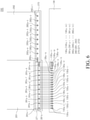
- a display device according to another embodiment will be described with reference to FIG. 6 . Since the difference between the display device according to an exemplary embodiment and the display device according to another exemplary embodiment is only a configuration of the cable, the configuration of the cable will be mainly described and a redundant description will be omitted.
- FIG. 6 is a view for explaining a connection relationship of a cable and a driving printed circuit board of a display device according to another exemplary embodiment.
- a plurality of first cable pins 261p is disposed at both ends of a first cable unit 261. Further, in the first cable pins 261p, a connection hole 261c extending in an arrangement direction of the first cable pins 261p is formed.
- connection hole 261c extends in the arrangement direction of the first cable pins 261p, but it is not limited thereto and the connection hole 261c may be divided into a plurality of connection holes.
- a plurality of second cable pins 262p is disposed on an extending line of the connection hole 261c formed in the first cable unit 261 at both ends of the second cable unit 262.
- the plurality of first cable pins 261p and the plurality of second cable pins 262p are disposed in the same direction, but on different lines when the second cable unit 262 is unfolded with respect to the first cable unit 261.
- the display device 200 when a hinge connecting module 270 (271, 272) is folded so that the first cable unit 261 and the second cable unit 262 overlap each other, the plurality of second cable pin 262p passes through the connection hole 261c to be connected to the corresponding contact pad 130p of the driving printed circuit board 130.
- a 1-1-th cable pin 261p-1 is in direct contact with the first contact pad 130p-1
- a 2-1-th cable pin 262p-1 passes through the connection hole 261c to be in contact with the second contact pad 130p-2
- a 1-2-th cable pin 261p-2 is in direct contact with the third contact pad 130p-3
- a 2-2-th cable pin 262p-2 passes through the connection hole 261c to be in contact with the fourth contact pad 130p-4
- a 1-3-th cable pin 261p-3 is in direct contact with the fifth contact pad 130p-5
- a 2-3-th cable pin 262p-3 passes through the connection hole 261c to be in contact with the sixth contact pad 130p-6
- a 1-4-th cable pin 261p-4 is in direct contact with the seventh contact pad 130p-7
- a 2-4-th cable pin 262p-4 passes through the connection hole 261c to be in contact with the eighth contact pad 130p-8
- the plurality of first cable pins 261p and the plurality of second cable pins 262p are disposed on different lines.
- the hinge connecting module 270 of the display device 200 when the hinge connecting module 270 of the display device 200 according to another exemplary embodiment is folded so that the first cable unit 261 and the second cable unit 262 overlap each other, the plurality of first cable pins 261p and the plurality of second cable pins 262p are spaced apart from each other. Therefore, confusion in the transmission of the image signal caused by the contact of the first cable pin 261p and the second cable pin 262p may be avoided.
- the cables 261 and 262 are folded using the hinge connecting module 270 to be in contact with the contact pad 130p. Therefore, as the number of driving printed circuit boards 130 which may be attached to the display panel is increased, the resolution to be implemented by the display device 200 may be increased.
- the plurality of first cable pins 261p and the plurality of second cable pins 262p are disposed on different lines to suppress the screen failure.
- a display device includes: a display panel, a driving printed circuit board connected to the display panel, a control printed circuit board connected to the driving printed circuit board, at least one cable which connects the driving printed circuit board and the control printed circuit board, and a hinge connecting module disposed at both ends of at least one cable. Therefore, it is possible to implement an image having a high resolution by increasing the number of driving printed circuit boards attached to the display panel.
- the hinge connecting module may include a first hinge unit which is disposed on the driving printed circuit board and the control printed circuit board and a second hinge unit which axially rotates with respect to a hinge shaft to be hinge coupled to the first hinge unit.
- the at least one cable may include a first cable unit coupled to the first hinge unit and a second cable unit coupled to the second hinge unit.
- the second cable unit may be folded in a direction of one surface of the first cable unit by the hinge connecting module.
- the second cable unit may overlap the first cable unit.
- a plurality of first cable pins may be disposed at both ends of the first cable unit and a plurality of second cable pins may be disposed at both ends of the second cable unit.
- Each of the driving printed circuit board and the control printed circuit board may include a plurality of contact pads, and the plurality of first cable pins and the second cable pins are connected to the plurality of contact pads.
- a plurality of connection holes may be formed between the plurality of first cable pins and the plurality of second cable pins may be inserted into the plurality of connection holes to be electrically connected to the plurality of contact pads.
- the plurality of first cable pins and the plurality of second cable pins are disposed on the same line.
- At least one connection hole may be formed at one side of the plurality of first cable pins, the plurality of first cable pins and the plurality of second cable pins may be disposed on different lines, the plurality of second cable pins and the at least one connection hole may be disposed on the same line, and the plurality of second cable pins may be inserted into the plurality of connection holes to be electrically connected to the plurality of contact pads.
- An interval between the plurality of contact pads may be narrower than an interval between the plurality of first cable pins and an interval between the plurality of second cable pins.
- a first cable pin adjacent to the hinge shaft among the plurality of first cable pins and a second cable pin adjacent to the hinge shaft among the plurality of second cable pin correspond to power cable pins.
Landscapes
- Engineering & Computer Science (AREA)
- Physics & Mathematics (AREA)
- Theoretical Computer Science (AREA)
- General Physics & Mathematics (AREA)
- Computer Hardware Design (AREA)
- Mathematical Physics (AREA)
- General Engineering & Computer Science (AREA)
- Human Computer Interaction (AREA)
- Nonlinear Science (AREA)
- Microelectronics & Electronic Packaging (AREA)
- Optics & Photonics (AREA)
- Crystallography & Structural Chemistry (AREA)
- Chemical & Material Sciences (AREA)
- Devices For Indicating Variable Information By Combining Individual Elements (AREA)
- Manufacturing & Machinery (AREA)
Description
- The present disclosure relates to a device comprising a printed circuit board and a hinged connecting module.
- Currently, as it enters a full-scale information era, a field of a display device which visually expresses electrical information signals has been rapidly developed and studies are continued to improve performances of various display devices such as a thin thickness, a light weight, and low power consumption. Examples of such a display device include a liquid crystal display device (LCD), a plasma display panel device (PDP), a field emission display device (FED), an electro-wetting display device (EWD), and an organic light emitting display device (OLED).
- Various types of display devices include data lines and driving circuit units for driving the data lines to implement images. That is, the driving circuit unit is applied with an image signal from the outside through a cable and converts the image in accordance with a display timing to output the converted image to the data line so that the display device implements images.
- Recently, in order to implement realistic images, a large number of data lines and driving circuit units are necessary to implement a high resolution such as 8k resolution (7680 × 4320). However, an area where the driving circuit units are disposed is limited in the display device so that there is a limitation to implement a high resolution by increasing the number of driving circuit units.
-
EP 0 297 699 A2 discloses an electrical connector for a flat cable having alternate signal and ground conductors comprises a movable part in which an array of sockets having rearwardly extending contact pins is mounted in an insulating housing and surrounded by upper and lower conductive shells, the signal conductors of the cable being fixed to the pins and the ground conductors being fixed to the shells. A fixed part comprises mating contacts and springy fingers fixed within housing for engagement of contacts in sockets of the movable part and engagement of springy fingers with the conductive shells. -
EP 2 876 746 A1 - The invention is as set out in
claim 1. - An object to be achieved by the present disclosure is to provide a display device which includes more integrated driving printed circuits.
- Another object to be achieved by the present disclosure is to provide a display device which implements a high resolution.
- Objects of the present disclosure are not limited to the above-mentioned objects, and other objects, which are not mentioned above, can be clearly understood by those skilled in the art from the following descriptions
- There is provided a display device including a display panel, a driving printed circuit board connected to the display panel, a control printed circuit board connected to the driving printed circuit board, at least one cable which connects the driving printed circuit board and the control printed circuit board, and a hinge connecting module (which may be described as a hinged connecting module) disposed at both ends of at least one cable. Therefore, it is possible to implement an image having a high resolution by increasing the number of driving printed circuit boards attached to the display panel.
- Other detailed matters of the exemplary embodiments are included in the detailed description and the drawings.
- According to the present disclosure, a size of the driving printed circuit board is reduced so that the number of driving printed circuit boards attached to the display panel is increased, thereby implementing a high-quality image.
- According to the present disclosure, a plurality of cable pins is disposed on different lines to suppress a contact failure at the time of folding the cable, thereby suppressing a screen failure.
- The effects according to the present disclosure are not limited to the contents exemplified above, and more various effects are included in the present specification.
- The above and other aspects, features and other advantages of the present disclosure will be more clearly understood from the following detailed description taken in conjunction with the accompanying drawings, in which:
-
FIG. 1 is a view illustrating a display device according to an embodiment; -
FIG. 2 is a cross-sectional view taken along the line I-I' ofFIG. 1 , according to an embodiment; -
FIG. 3 is a view for explaining a folded state of a hinge connecting module of a display device according to an embodiment; -
FIG. 4 is a view for explaining an unfolded state of a hinge connecting module of a display device according to an embodiment; -
FIG. 5 is a view for explaining a connection relationship of a cable and a driving printed circuit board of a display device according to an embodiment; and -
FIG. 6 is a view for explaining a connection relationship of a cable and a driving printed circuit board of a display device according to another embodiment. - Advantages and characteristics of the present disclosure and a method of achieving the advantages and characteristics will be clear by referring to exemplary embodiments described below in detail together with the accompanying drawings. However, the present disclosure is not limited to the exemplary embodiments disclosed herein but will be implemented in various forms. The exemplary embodiments are provided by way of example only so that those skilled in the art can fully understand the disclosures of the present disclosure and the scope of the present disclosure. Therefore, the present disclosure is defined only by the scope of the appended claims.
- The shapes, sizes, ratios, angles, numbers, and the like illustrated in the accompanying drawings for describing the exemplary embodiments are merely examples, and the present disclosure is not limited thereto. Like reference numerals generally denote like elements throughout the specification. Further, in the following description of the present disclosure, a detailed explanation of known related technologies may be omitted to avoid unnecessarily obscuring the subject matter of the present disclosure. The terms such as "including," "having," and "comprising" used herein are generally intended to allow other components to be added unless the terms are used with the term "only." Any references to singular may include plural unless expressly stated otherwise.
- Components are interpreted to include an ordinary error range even if not expressly stated.
- When the position relation between two parts is described using the terms such as "on," "above," "below," and "next," one or more parts may be positioned between the two parts unless the terms are used with the term "immediately" or "directly."
- When an element or layer is disposed "on" another element or layer, the other element may be interposed therebetween.
- Although the terms "first," "second," and the like are used for describing various components, these components are not confined by these terms. These terms are merely used for distinguishing one component from the other components. Therefore, a first component to be mentioned below may be a second component in a technical concept of the present disclosure.
- Like reference numerals generally denote like elements throughout the specification.
- A size and a thickness of each component illustrated in the drawing are illustrated for convenience of description, and the present disclosure is not limited to the size and the thickness of the component illustrated.
- The features of various embodiments can be partially or entirely adhered to or combined with each other and can be interlocked and operated in technically various ways, and the embodiments can be carried out independently of or in association with each other.
- Hereinafter, a display device according to exemplary embodiments will be described in detail with reference to accompanying drawings.
-
FIG. 1 is a view illustrating a display device according to an embodiment. - Specifically,
FIG. 1 is a rear view of adisplay device 100 according to an exemplary embodiment and illustrates adisplay panel 110, a driving integratedcircuit 120, and a driving printedcircuit board 130 which are accommodated in aback cover 140. - As illustrated in
FIG. 1 , thedisplay device 100 according to the exemplary embodiment includes thedisplay panel 110 which implements images, the driving integratedcircuit 120 which drives thedisplay panel 110, the driving printedcircuit board 130 which supports the drivingintegrated circuit 120, and theback cover 140 which accommodates thedisplay panel 110, the drivingintegrated circuit 120 and the driving printedcircuit board 130. - The
display device 100 according to the exemplary embodiment may further include a control printedcircuit board 150 disposed on a rear surface of theback cover 140, acable 160 which connects the driving printedcircuit board 130 and the control printedcircuit board 150, and ahinge connecting module 170. - As a coupling state of the
display device 100 including the above-described components of thedisplay device 100, in a state where the driving integratedcircuit 120 and the driving printedcircuit board 130 are disposed on the rear surface of thedisplay panel 110, theback cover 140 is coupled to thedisplay panel 110 on the rear surface of thedisplay panel 110 to be integrated. Thecable 160 passing through theback cover 140 connects the control printedcircuit board 150 and the driving printedcircuit board 130 through thehinge connecting module 170. - The
display panel 110 is a panel for displaying images. Thedisplay panel 110 may be any one of various display panels, such as an organic light emitting display panel, a liquid crystal display panel, a field emission display panel, and an electro-wetting display panel. Hereinafter, as an example, it is described that thedisplay panel 110 of thedisplay device 100 according to an exemplary embodiment is an organic light emitting display panel. -
FIG. 2 is a cross-sectional view taken along the line I-I' ofFIG. 1 . - Referring to
FIG. 2 , thedisplay device 100 according to the exemplary embodiment includes thedisplay panel 110 and theback cover 140 coupled to thedisplay panel 110. - The
display panel 110 includes afirst substrate 111, an organiclight emitting diode 112, aprotective layer 113, anadhesive layer 114, and asecond substrate 115. - The
first substrate 111 may be formed of a transparent and rigid material such as glass or a transparent flexible material. The organiclight emitting diode 112 formed for every unit pixel is disposed on thefirst substrate 111. Even though not illustrated in the drawing, a switching transistor, a driving transistor, and at least one capacitor for driving the organiclight emitting diode 112 are disposed between thefirst substrate 111 and the organiclight emitting diode 112. - The organic
light emitting diode 112 includes a first electrode which is supplied with currents from a driving transistor (not illustrated) disposed for every unit pixel, a second electrode corresponding to the first electrode, and an organic layer disposed between the first electrode and the second electrode. - The first electrode may be formed of a transparent electrode material and the second electrode may be formed of a metal material. The organic layer may include an organic light emitting layer which emits light, an electron injecting layer and a hole injecting layer which inject electrons and holes into the organic light emitting layer, respectively, an electron transport layer and a hole transport layer which transport the injected electrons and holes to the organic light emitting layer, respectively, and charge generating layers which generate charges such as the electrons and the holes.
- Hereinafter, an emission method of the organic
light emitting diode 112 will be described. The holes are injected into the organic layer from the first electrode to reach the organic light emitting layer through the hole injecting layer and the hole transport layer. Further, the electrons are injected into the organic layer from the second electrode to reach the organic light emitting layer through the electron injecting layer and the electron transport layer. In the organic light emitting layer, the holes and the electrons are coupled to form excitons and emit light. - The
protective layer 113 for protecting the organiclight emitting diode 112 is disposed on an upper surface and a side surface of the organiclight emitting diode 112. Theadhesive layer 114 is disposed on an upper surface and a side surface of theprotective layer 113 to bond thefirst substrate 111 and thesecond substrate 115. In this case, theadhesive layer 114 may include a moisture adsorbent which absorbs moisture to protect the organiclight emitting diode 112 from the moisture. - The
second substrate 115 which is opposite to thefirst substrate 111 is disposed on theadhesive layer 114. Thesecond substrate 115 is an encapsulation plate and for example, may be formed of one of glass, metal foil, and a plastic film. Here, the encapsulation plate may also be referred to as an encapsulation substrate. - However, the
display device 100 according to the exemplary embodiment is described to have a structure in which the organiclight emitting diode 112 is encapsulated by theprotective layer 113 and theadhesive layer 114, but it is not limited thereto. The display device may have an encapsulation structure in which an adhesive such as sealant is applied on an outer edge of thefirst substrate 111 and thesecond substrate 115. - The driving
integrated circuit 120 is a configuration for processing a data voltage for displaying images and various driving signals for processing the data voltage, and outputs various control signals to thedisplay panel 110. - Further, the driving
integrated circuit 120 may sense a characteristic deviation of the organiclight emitting diode 112 and the transistor disposed in the plurality of pixels, for example, luminance deviation between pixels such as a deviation due to the change of a threshold voltage or a mobility of the plurality of transistors or a deviation due to the deterioration of the organiclight emitting diode 112 to compensate the data voltage. The drivingintegrated circuit 120 may transmit the compensated data voltage to the plurality of data lines. - Further, the driving
integrated circuit 120 digitalizes a voltage which is an analog format to store the digitalized voltage. To this end, the drivingintegrated circuit 120 may include an analog digital converter (ADC) and a digital analog converter (DAC). That is, the drivingintegrated circuit 120 may be defined as a configuration including a compensating circuit. - Even though in
FIG. 1 , it is illustrated that the drivingintegrated circuit 120 is implemented by a chip on film (COF) manner, it is not limited thereto and the drivingintegrated circuit 120 may be disposed by a chip on glass (COG) manner or a tape carrier package (TCP) manner. - The driving printed
circuit board 130 is connected to the control printedcircuit board 150 through thecable 160 and thehinge connecting module 170 to control the drivingintegrated circuit 120. - That is, the driving printed
circuit board 130 is applied with an image signal from the control printedcircuit board 150 to generate a gate control signal, a data control signal, and a power signal for controlling the drivingintegrated circuit 120 and output the signals to the drivingintegrated circuit 120. - Further, as illustrated in
FIG. 1 , the driving printedcircuit board 130 may be disposed between thedisplay panel 110 and theback cover 140. More specifically, the driving printedcircuit board 130 is disposed on a rear surface of thedisplay panel 110, but is not limited thereto and a position where the driving printedcircuit board 130 is disposed may vary. - The
back cover 140 accommodates thedisplay panel 110 and is bonded to the rear surface of thesecond substrate 115 by means of the adhesive layer. - The
back cover 140 may be formed of any one of aluminum (Al), copper (Cu), zinc (Zn), silver (Ag), gold (Au), or iron (Fe) having a high thermal conductivity or an alloy of the above-mentioned metals. More specifically, theback cover 140 is desirably formed of aluminum (Al) which has a high thermal conductivity, light weight, and a low cost. - The control printed
circuit board 150 receives an image or audio signal input from the outside to transmit the image or audio signal to thedisplay panel 110 or a speaker (not illustrated) to control a display or an audio output. - In other words, the control printed
circuit board 150 is connected to the driving printedcircuit board 130 by means of thehinge connecting module 170 and thecable 160. The control printedcircuit board 150 may output the image signal and the audio signal to the driving printedcircuit board 130. - Hereinafter, a coupling relationship of the driving printed
circuit board 130, thecable 160, and thehinge connecting module 170 of thedisplay device 100 according to an exemplary embodiment will be described. -
FIG. 3 is a view for explaining a folded state of a hinge connecting module of a display device according to an exemplary embodiment.FIG. 4 is a view for explaining an unfolded state of a hinge connecting module of a display device according to an exemplary embodiment. - For the convenience of description,
FIGS. 3 and4 illustrate only a coupling relationship between the driving printedcircuit board 130 and thehinge connecting module 170. The coupling relationship between the control printedcircuit board 150 and thehinge connecting module 170 is the same as the coupling relationship between the driving printedcircuit board 130 and thehinge connecting module 170 so that the coupling relationship between the driving printedcircuit board 130 and thehinge connecting module 170 will be mainly described. - Referring to
FIGS. 3 and4 , thehinge connecting module 170 of thedisplay device 100 according to the exemplary embodiment includes afirst hinge unit 171 disposed on the driving printedcircuit board 130, asecond hinge unit 172 hinge coupled to one side of thefirst hinge unit 171, and ahinge shaft 173 which hinge couples thefirst hinge unit 171 and thesecond hinge unit 172. - Specifically, the
first hinge unit 171 is fixed onto the driving printedcircuit board 130. Thesecond hinge unit 172 hinge coupled to one side of thefirst hinge unit 171 by means of thehinge shaft 173 may axially rotate with respect to thehinge shaft 173, or at least axially rotate with respect to the axis of the hinge shaft. - For the purpose of the hinge coupling, an inner accommodating space of the
first hinge unit 171 needs to be larger than an outer edge of thesecond hinge unit 172 to accommodate thesecond hinge unit 172, according to some embodiments. Specifically, in these embodiments, an inner width of thefirst hinge unit 171 needs to be equal to or larger than a width of the outer edge of thesecond hinge unit 172 in an extending direction of thehinge shaft 173. Further in some embodiments, an inner length of thefirst hinge unit 171 needs to be equal to or larger than a length of the outer edge of thesecond hinge unit 172 in a vertical direction of the extending direction of thehinge shaft 173. - The
cable 160 is divided with respect to a portion coupled to thehinge connecting module 170. That is, thecable 160 may be divided into afirst cable unit 161 which is coupled to thefirst hinge unit 171 and asecond cable unit 162 which is coupled to thesecond hinge unit 172. - The
first cable unit 161 is coupled to thefirst hinge unit 171 fixed onto the driving printedcircuit board 130 so that thefirst cable unit 161 may also be fixed onto the driving printedcircuit board 130. - The
second cable unit 162 is coupled to thesecond hinge unit 172 which is folded with respect to thehinge shaft 173 so that thesecond cable unit 162 is also folded with respect to thehinge shaft 173. - Specifically, as illustrated in
FIG. 3 , when thehinge connecting module 170 of thedisplay device 100 according to the exemplary embodiment is folded, thesecond hinge unit 172 is hinged to thefirst hinge unit 171. Therefore, thesecond cable unit 162 which is coupled to thesecond hinge unit 172 is also inwardly folded in an upper surface direction of thefirst cable unit 161 to overlap each other. - As illustrated in
FIG. 4 , a plurality offirst cable pins 161p is disposed at both ends of thefirst cable unit 161 and a plurality ofsecond cable pins 162p is disposed at both ends of thesecond cable unit 162. The first cable pins 161p and the second cable pins 162p may be disposed in thehinge connecting module 170. - Specifically, the plurality of
first cable pins 161p may be disposed in thefirst hinge unit 171 connected to thefirst cable unit 161. The plurality of second cable pins 162p may be disposed in thesecond hinge unit 172 connected to thesecond cable unit 162. -
FIG. 5 is a view for explaining a connection relationship of a cable and a driving printed circuit board of a display device according to an exemplary embodiment. - In order to apply the image signal and the power voltage to the driving printed
circuit board 130, the plurality of first cable pins 161p and the plurality of second cable pins 162p may be connected to a plurality ofcontact pads 130p disposed on the driving printedcircuit board 130. - Specifically, as illustrated in
FIG. 5 , the plurality offirst cable pins 161p includes a 1-1-th cable pin 161p-1, a 1-2-th cable pin 161p-2, a 1-3-th cable pin 161p-3, a 1-4-th cable pin 161p-4, a 1-5-th cable pin 161p-5, a 1-6-th cable pin 161p-6, a 1-7-th cable pin 161p-7, a 1-8-th cable pin 161p-8, a 1-9-th cable pin 161p-9, and a 1-10-th cable pin 161p-10 which are sequentially disposed toward the hinge shaft direction. - Further, the plurality of
second cable pins 162p includes a 2-1-th cable pin 162p-1, a 2-2-th cable pin 162p-2, a 2-3-th cable pin 162p-3, a 2-4-th cable pin 162p-4, a 2-5-th cable pin 162p-5, a 2-6-th cable pin 162p-6, a 2-7-th cable pin 162p-7, a 2-8-th cable pin 162p-8, a 2-9-th cable pin 162p-9, and a 2-10-th cable pin 162p-10 which are sequentially disposed toward the hinge shaft direction. - On the driving printed
circuit board 130, afirst contact pad 130p-1 to anineteenth contact pad 130p-19 which are in direct contact with the plurality of first cable pins 161p and the plurality of second cable pins 162p are included. - Here, the 1-1-
th cable pin 161p-1 to 1-9-th cable pin 161p-9 and the 2-1-th cable pin 162p-1 to 2-9-th cable pin 162p-9 may be cable pins which transmit the image signal to the driving printedcircuit board 130 and the 1-10-th cable pin 161p-10 and the 2-10-th cable pin 162p-10 may be cable pins which transmit the power voltage. - To this end, sizes of the 1-10-
th cable pin 161p-10 and the 2-10-th cable pin 162p-10 may be larger than sizes of the 1-1-th cable pin 161p-1 to 1-9-th cable pin 161p-9 and the 2-1-th cable pin 162p-1 to 2-9-th cable pin 162p-9. Further, the 1-10-th cable pin 161p-10 may be disposed to be adjacent to thehinge shaft 173 among the plurality offirst cable pin 161p. Similarly, the 2-10-th cable pin 162p-10 may be disposed to be adjacent to thehinge shaft 173 among the plurality ofsecond cable pin 162p. - By doing this, the 1-10-
th cable pin 161p-10 and the 2-10-th cable pin 162p-10 corresponding to power cable pins are disposed to be adjacent to thehinge shaft 173 and have a relatively larger size. Therefore, in the folded state, the 1-10-th cable pin 161p-10 and the 2-10-th cable pin 162p-10 overlap each other without being connected to other cable pins to be stably connected to thenineteenth contact pad 130p-19 so that the power voltage may be stably supplied. - Further, the
first cable pin 161p and thesecond cable pin 162p excluding the 1-10-th cable pin 161p-10 and the 2-10-th cable pin 162p-10 are alternately connected to the plurality ofcontact pads 130p. Therefore, the driving printedcircuit board 130 may be applied with the image signal from the control printedcircuit board 150. - Specifically, the 1-1-
th cable pin 161p-1 is in contact with thefirst contact pad 130p-1, the 1-2-th cable pin 161p-2 is in contact with thethird contact pad 130p-3, the 1-3-th cable pin 161p-3 is in contact with thefifth contact pad 130p-5, the 1-4-th cable pin 161p-4 is in contact with theseventh contact pad 130p-7, the 1-5-th cable pin 161p-5 is in contact with theninth contact pad 130p-9, the 1-6-th cable pin 161p-6 is in contact with theeleventh contact pad 130p-11, the 1-7-th cable pin 161p-7 is in contact with thethirteenth contact pad 130p-13, the 1-8-th cable pin 161p-8 is in contact with thefifteenth contact pad 130p-15, and the 1-9-th cable pin 161p-9 is in contact with theseventeenth contact pad 130p-17. - When the
second hinge unit 172 is hinged to thefirst hinge unit 171, the plurality of second cable pins 162p passes through a plurality of connection holes 161c to be connected to thecontact pad 130p on the driving printedcircuit board 130. - Specifically, the 2-1-th cable pin 162p-1 is connected to a second contact pad 130p-2 through a first connection hole 161c-1, the 2-2-th cable pin 162p-2 is connected to a fourth contact pad 130p-4 through a second connection hole 161c-2, the 2-3-th cable pin 162p-3 is connected to a sixth contact pad 130p-6 through a third connection hole 161c-3, the 2-4-th cable pin 162p-4 is connected to an eighth contact pad 130p-8 through a fourth connection hole 161c-4, the 2-5-th cable pin 162p-5 is connected to a tenth contact pad 130p-10 through a fifth connection hole 161c-5, the 2-6-th cable pin 162p-6 is connected to a twelfth contact pad 130p-12 through a sixth connection hole 161c-6, the 2-7-th cable pin 162p-7 is connected to a fourteenth contact pad 130p-14 through a seventh connection hole 161c-7, the 2-8-th cable pin 162p-8 is connected to a sixteenth contact pad 130p-16 through an eighth connection hole 161c-8, and the 2-9-th cable pin 162p-9 is connected to an eighteenth contact pad 130p-18 through a ninth connection hole 161c-9.
- As described above, in a state when the
first cable unit 161 and thesecond cable unit 162 are folded by thehinge connecting module 170, the plurality of first cable pins 161p and the plurality of second cable pins 162p may be connected to thecontact pad 130p. - Therefore, an interval PI between the plurality of first cable pins 161p or an interval PI between the plurality of second cable pins 162p may be larger than an interval between the plurality of
contact pads 130p. - Here, the interval PI between the plurality of first cable pins 161p or the interval PI between the plurality of
second cable pins 162p refers to an interval P1 between centers of the first cable pins 161p or an interval PI between centers of the plurality of second cable pins 162p. Further, the interval between the plurality ofcontact pads 130p refers to an interval between centers of the plurality ofcontact pads 130p. - Specifically, the interval PI between the plurality of first cable pins 161p or the interval PI between the plurality of second cable pins 162p may be twice the interval between the plurality of
contact pads 130p. - For example, the interval PI between the plurality of first cable pins 161p or the interval PI between the plurality of second cable pins 162p may be 0.5 mm and the interval P2 between the
contact pads 130p may be 0.25 mm. - That is, the
display device 100 according to the exemplary embodiment includes ahinge connecting module 170 so that thecable 160 is folded to be electrically connected to the plurality ofcontact pads 130p of the driving printedcircuit board 130. - Therefore, the interval of the
contact pads 130p of the driving printedcircuit board 130 may be reduced by half and thus, an area where thecontact pads 130p are disposed in the driving printedcircuit board 130 may also be reduced. - Accordingly, the
display device 100 according to the exemplary embodiment may reduce the size of the driving printedcircuit board 130 so that the number of driving printedcircuit boards 130 attached to thedisplay panel 110 may be increased. - Therefore, as the number of driving printed
circuit boards 130 is increased, the resolution to be implemented by thedisplay device 100 according to the exemplary embodiment may be increased. - Hereinafter, a display device according to another embodiment will be described with reference to
FIG. 6 . Since the difference between the display device according to an exemplary embodiment and the display device according to another exemplary embodiment is only a configuration of the cable, the configuration of the cable will be mainly described and a redundant description will be omitted. -
FIG. 6 is a view for explaining a connection relationship of a cable and a driving printed circuit board of a display device according to another exemplary embodiment. - Referring to
FIG. 6 , in adisplay device 200 according to another exemplary embodiment, a plurality offirst cable pins 261p is disposed at both ends of afirst cable unit 261. Further, in thefirst cable pins 261p, aconnection hole 261c extending in an arrangement direction of thefirst cable pins 261p is formed. - In
FIG. 6 , it is illustrated that theconnection hole 261c extends in the arrangement direction of thefirst cable pins 261p, but it is not limited thereto and theconnection hole 261c may be divided into a plurality of connection holes. - Further, a plurality of
second cable pins 262p is disposed on an extending line of theconnection hole 261c formed in thefirst cable unit 261 at both ends of thesecond cable unit 262. - That is, the plurality of first cable pins 261p and the plurality of second cable pins 262p are disposed in the same direction, but on different lines when the
second cable unit 262 is unfolded with respect to thefirst cable unit 261. - Therefore, in the
display device 200 according to another exemplary embodiment, when a hinge connecting module 270 (271, 272) is folded so that thefirst cable unit 261 and thesecond cable unit 262 overlap each other, the plurality ofsecond cable pin 262p passes through theconnection hole 261c to be connected to thecorresponding contact pad 130p of the driving printedcircuit board 130. - Specifically, in the display device 200 according to another exemplary embodiment, when the hinge connecting module 270 is folded, a 1-1-th cable pin 261p-1 is in direct contact with the first contact pad 130p-1, a 2-1-th cable pin 262p-1 passes through the connection hole 261c to be in contact with the second contact pad 130p-2, a 1-2-th cable pin 261p-2 is in direct contact with the third contact pad 130p-3, a 2-2-th cable pin 262p-2 passes through the connection hole 261c to be in contact with the fourth contact pad 130p-4, a 1-3-th cable pin 261p-3 is in direct contact with the fifth contact pad 130p-5, a 2-3-th cable pin 262p-3 passes through the connection hole 261c to be in contact with the sixth contact pad 130p-6, a 1-4-th cable pin 261p-4 is in direct contact with the seventh contact pad 130p-7, a 2-4-th cable pin 262p-4 passes through the connection hole 261c to be in contact with the eighth contact pad 130p-8, a 1-5-th cable pin 261p-5 is in direct contact with the ninth contact pad 130p-9, a 2-5-th cable pin 262p-5 passes through the connection hole 261c to be in contact with the tenth contact pad 130p-10, a 1-6-th cable pin 261p-6 is in direct contact with the eleventh contact pad 130p-11, a 2-6-th cable pin 262p-6 passes through the connection hole 261c to be in contact with the twelfth contact pad 130p-12, a 1-7-th cable pin 261p-7 is in direct contact with the thirteenth contact pad 130p-13, a 2-7-th cable pin 262p-7 passes through the connection hole 261c to be in contact with the fourteenth contact pad 130p-14, a 1-8-th cable pin 261p-8 is in direct contact with the fifteenth contact pad 130p-15, a 2-8-th cable pin 262p-8 passes through the connection hole 261c to be in contact with the sixteenth contact pad 130p-16, a 1-9-th cable pin 261p-9 is in direct contact with the seventeenth contact pad 130p-17, a 2-9-th cable pin 262p-9 passes through the connection hole 261c to be in contact with the eighteenth contact pad 130p-18, a 1-10-th cable pin 261p-10 is in direct contact with the nineteenth contact pad 130p-19, and a 2-10-th cable pin 262p-10 passes through the connection hole 261c to be in contact with the nineteenth contact pad 130p-19.
- As described above, in the
display device 200 according to another exemplary embodiment, the plurality of first cable pins 261p and the plurality of second cable pins 262p are disposed on different lines. - Therefore, when the hinge connecting module 270 of the
display device 200 according to another exemplary embodiment is folded so that thefirst cable unit 261 and thesecond cable unit 262 overlap each other, the plurality of first cable pins 261p and the plurality of second cable pins 262p are spaced apart from each other. Therefore, confusion in the transmission of the image signal caused by the contact of thefirst cable pin 261p and thesecond cable pin 262p may be avoided. - That is, in the
display device 200 according to another exemplary embodiment, thecables contact pad 130p. Therefore, as the number of driving printedcircuit boards 130 which may be attached to the display panel is increased, the resolution to be implemented by thedisplay device 200 may be increased. - Further, in the
display device 200 according to another exemplary embodiment, the plurality of first cable pins 261p and the plurality of second cable pins 262p are disposed on different lines to suppress the screen failure. - The exemplary embodiments can also be described as follows:
- According to an aspect of the present disclosure, a display device includes: a display panel, a driving printed circuit board connected to the display panel, a control printed circuit board connected to the driving printed circuit board, at least one cable which connects the driving printed circuit board and the control printed circuit board, and a hinge connecting module disposed at both ends of at least one cable. Therefore, it is possible to implement an image having a high resolution by increasing the number of driving printed circuit boards attached to the display panel.
- The hinge connecting module may include a first hinge unit which is disposed on the driving printed circuit board and the control printed circuit board and a second hinge unit which axially rotates with respect to a hinge shaft to be hinge coupled to the first hinge unit.
- The at least one cable may include a first cable unit coupled to the first hinge unit and a second cable unit coupled to the second hinge unit.
- The second cable unit may be folded in a direction of one surface of the first cable unit by the hinge connecting module.
- The second cable unit may overlap the first cable unit.
- A plurality of first cable pins may be disposed at both ends of the first cable unit and a plurality of second cable pins may be disposed at both ends of the second cable unit.
- Each of the driving printed circuit board and the control printed circuit board may include a plurality of contact pads, and the plurality of first cable pins and the second cable pins are connected to the plurality of contact pads.
- A plurality of connection holes may be formed between the plurality of first cable pins and the plurality of second cable pins may be inserted into the plurality of connection holes to be electrically connected to the plurality of contact pads.
- The plurality of first cable pins and the plurality of second cable pins are disposed on the same line.
- At least one connection hole may be formed at one side of the plurality of first cable pins, the plurality of first cable pins and the plurality of second cable pins may be disposed on different lines, the plurality of second cable pins and the at least one connection hole may be disposed on the same line, and the plurality of second cable pins may be inserted into the plurality of connection holes to be electrically connected to the plurality of contact pads.
- An interval between the plurality of contact pads may be narrower than an interval between the plurality of first cable pins and an interval between the plurality of second cable pins.
- A first cable pin adjacent to the hinge shaft among the plurality of first cable pins and a second cable pin adjacent to the hinge shaft among the plurality of second cable pin correspond to power cable pins.
- Although the exemplary embodiments have been described in detail with reference to the accompanying drawings, the present disclosure is not limited thereto and may be embodied in many different forms without departing from the scope of the appended claims. Therefore, the exemplary embodiments are provided for illustrative purposes only and are not intended to limit the scope of the appended claims. Therefore, it should be understood that the above-described exemplary embodiments are illustrative in all aspects and do not limit scope of the appended claims. The protective scope of the present disclosure should be construed based on the following claims.
Claims (11)
- A device, comprising:a printed circuit board (130) having a plurality of contact pads (130p) disposed thereon; anda hinged connecting module, comprising:a first hinge unit (171, 271) coupled to a first cable unit (161, 261) of a cable;a second hinge unit (172, 272) coupled to a second cable unit (162, 262) of the cable; anda hinge shaft (173) coupling the first hinge unit and the second hinge unit,at least one connection hole (161c, 261c) disposed in the first hinge unit,a plurality of first cable pins (161p, 261p) disposed in the first hinge unit and connected to corresponding ones of the contact pads, anda plurality of second cable pins (162p, 262p) disposed in the second hinge unit;wherein the second hinge unit is arranged to rotate with respect to the axis of the hinge shaft to overlap the first hinge unit, andthe device is arranged so that when the second hinge unit overlaps the first hinge unit, the second cable pins are inserted into corresponding ones of the at least one connection hole and connected to corresponding ones of the contact pads.
- The device of claim 1,wherein the at least one connection hole is disposed at one side of a plurality of first cable pins (161p),wherein a first line along which the plurality of first cable pins are disposed and a second line along which the plurality of second cable pins are disposed are offset from each other,wherein the at least one connection hole is disposed on the second line.
- The device of claim 1 or 2, wherein the at least one connection hole comprises a plurality of connection holes, and the number of connection holes is equal to the number of second cable pins.
- The device of claim 3, wherein the plurality of connection holes are arranged on the same line.
- The device of claim 3 or 4, wherein positions of the connection holes are disposed to correspond to positions of the second cable pins when the second hinge unit overlaps the first hinge unit.
- The device of claim 1, wherein the at least one connection hole comprises one or more elongated connection holes, the elongated connection holes extending along an arrangement direction of first cable pins of the first cable unit.
- The device of claim 6, wherein the one or more elongated connection holes are disposed between adjacent first cable pins.
- The device of claims 6 or 7, wherein the one or more elongated connection holes are arranged on the same line.
- The device of any of claims 1-8, wherein a first cable pin (161p-10) nearest the hinge shaft among the plurality of first cable pins and a second cable pin (162p-10) nearest the hinge shaft among the plurality of second cable pins correspond to power cable pins.
- The device of any preceding claim, wherein the printed circuit board comprises a driving printed circuit board (130) or a control printed circuit board (150).
- The device of any preceding claim, wherein an interval between the plurality of contact pads is narrower than an interval between the plurality of first cable pins and an interval between the plurality of second cable pins.
Applications Claiming Priority (1)
| Application Number | Priority Date | Filing Date | Title |
|---|---|---|---|
| KR1020180160934A KR102562804B1 (en) | 2018-12-13 | 2018-12-13 | Display device |
Publications (2)
| Publication Number | Publication Date |
|---|---|
| EP3667830A1 EP3667830A1 (en) | 2020-06-17 |
| EP3667830B1 true EP3667830B1 (en) | 2022-02-02 |
Family
ID=68886950
Family Applications (1)
| Application Number | Title | Priority Date | Filing Date |
|---|---|---|---|
| EP19215413.6A Active EP3667830B1 (en) | 2018-12-13 | 2019-12-11 | Device comprising a printed circuit board and a hinged connecting module. |
Country Status (5)
| Country | Link |
|---|---|
| US (1) | US11079637B2 (en) |
| EP (1) | EP3667830B1 (en) |
| JP (1) | JP6908681B2 (en) |
| KR (1) | KR102562804B1 (en) |
| CN (1) | CN111326080B (en) |
Families Citing this family (1)
| Publication number | Priority date | Publication date | Assignee | Title |
|---|---|---|---|---|
| EP4571718A4 (en) * | 2022-08-12 | 2025-12-10 | Panasonic Ip Man Co Ltd | DISPLAY DEVICE |
Family Cites Families (27)
| Publication number | Priority date | Publication date | Assignee | Title |
|---|---|---|---|---|
| US3356905A (en) * | 1966-11-29 | 1967-12-05 | Bendix Corp | Axial conductor locator |
| US4058890A (en) * | 1975-10-15 | 1977-11-22 | Hewlett-Packard Company | Method for mounting printed circuit boards |
| US4307438A (en) * | 1980-01-04 | 1981-12-22 | Augat Inc. | Hinged back panel input/output board |
| US4773878A (en) * | 1987-07-02 | 1988-09-27 | W. L. Gore & Associates | Shielded flat cable connectors |
| JP4200262B2 (en) | 2001-08-30 | 2008-12-24 | パナソニック電工株式会社 | Hinge connector |
| US7251512B2 (en) | 2002-05-13 | 2007-07-31 | Nec Corporation | Water-proof collapsible cellular terminal apparatus |
| US6945504B2 (en) | 2002-08-20 | 2005-09-20 | King Slide Works Co., Ltd. | Adjustable cable management arm for furniture |
| BR0205050A (en) | 2002-11-25 | 2004-06-29 | Multibras Eletrodomesticos Sa | Refrigerator and freezer door power supply system |
| KR20070000938A (en) | 2005-06-28 | 2007-01-03 | 엘지전자 주식회사 | Foldable Electronics |
| KR20080039613A (en) * | 2006-11-01 | 2008-05-07 | 엘지디스플레이 주식회사 | LCD Display |
| KR101296661B1 (en) | 2009-05-29 | 2013-08-14 | 엘지디스플레이 주식회사 | Liquid crystal display device |
| KR101749302B1 (en) * | 2010-12-24 | 2017-06-21 | 삼성전자주식회사 | Display apparatus |
| CN103579857B (en) * | 2012-07-23 | 2016-06-01 | 陳亮合 | High-frequency signal double-layer flat cable adapter card |
| US9538117B2 (en) * | 2013-01-07 | 2017-01-03 | Samsung Electronics Co., Ltd. | Support frame and display device including the same |
| JP2014010445A (en) | 2013-02-28 | 2014-01-20 | Takahisa Yamaguchi | Display device and method of manufacturing the same |
| WO2014132450A1 (en) | 2013-03-01 | 2014-09-04 | 株式会社日立産機システム | Oil-filled transformer |
| JP5979313B2 (en) * | 2013-04-30 | 2016-08-24 | 富士通株式会社 | Multi-divided housing coupling device and electronic device including the coupling device |
| KR102032383B1 (en) * | 2013-06-03 | 2019-11-11 | 삼성디스플레이 주식회사 | Display panel and manufacturing method thereof |
| KR20140148241A (en) | 2013-06-21 | 2014-12-31 | 삼성디스플레이 주식회사 | Adhesive display panel, connector and adhesive display system including thereof |
| KR102205030B1 (en) * | 2013-12-17 | 2021-01-20 | 삼성디스플레이 주식회사 | Display device |
| US9541962B2 (en) * | 2014-10-16 | 2017-01-10 | Microsoft Technology Licensing, Llc | Mobile computing device having a flexible hinge structure |
| KR102343892B1 (en) * | 2015-01-15 | 2021-12-27 | 삼성디스플레이 주식회사 | Flexible display device |
| US9728912B2 (en) * | 2015-12-08 | 2017-08-08 | Intel Corporation | Micro-coax cable adaptor board |
| KR20170080317A (en) * | 2015-12-31 | 2017-07-10 | 엘지디스플레이 주식회사 | Display device |
| EP3333453B1 (en) | 2016-12-09 | 2020-12-09 | Goodrich Actuation Systems Limited | Anti-rotational locking device |
| CN207040050U (en) | 2017-06-12 | 2018-02-23 | 深圳富泰宏精密工业有限公司 | Folding casing and the electronic installation with the housing |
| CN208478651U (en) | 2018-06-05 | 2019-02-05 | 温州意华接插件股份有限公司 | Connector mould group |
-
2018
- 2018-12-13 KR KR1020180160934A patent/KR102562804B1/en active Active
-
2019
- 2019-12-04 CN CN201911227363.8A patent/CN111326080B/en active Active
- 2019-12-04 US US16/703,586 patent/US11079637B2/en active Active
- 2019-12-06 JP JP2019220819A patent/JP6908681B2/en active Active
- 2019-12-11 EP EP19215413.6A patent/EP3667830B1/en active Active
Non-Patent Citations (1)
| Title |
|---|
| None * |
Also Published As
| Publication number | Publication date |
|---|---|
| KR20200072874A (en) | 2020-06-23 |
| US20200192141A1 (en) | 2020-06-18 |
| JP6908681B2 (en) | 2021-07-28 |
| CN111326080A (en) | 2020-06-23 |
| EP3667830A1 (en) | 2020-06-17 |
| US11079637B2 (en) | 2021-08-03 |
| KR102562804B1 (en) | 2023-08-01 |
| JP2020095270A (en) | 2020-06-18 |
| CN111326080B (en) | 2022-05-13 |
Similar Documents
| Publication | Publication Date | Title |
|---|---|---|
| US10993337B2 (en) | Display device | |
| US11087648B2 (en) | Display device | |
| KR101736930B1 (en) | Flexible organic light emitting display device | |
| US7884540B2 (en) | Organic light emitting diode display with flexible conductive film | |
| CN105551435B (en) | Display device with cap-type power supply | |
| US20250107000A1 (en) | Flexible circuit film and display apparatus having the same | |
| KR20190085199A (en) | Display apparatus and portable terminal | |
| US10490504B2 (en) | Chip on printed circuit unit and display apparatus comprising the same | |
| US20110164023A1 (en) | Organic light emitting diode display | |
| KR20180058879A (en) | Emi shielding film and display device including the same | |
| US11877483B2 (en) | Display device with circuit film coupled to lateral surface of base substrate | |
| KR20190139441A (en) | Display device having jointing auxiliary member | |
| US11079637B2 (en) | Display device | |
| EP3660909A1 (en) | Display apparatus | |
| CN113066393B (en) | Display device | |
| CN115206191B (en) | Electronic equipment | |
| KR20200030207A (en) | Display device | |
| KR20140042657A (en) | Display device having a flexible film cable | |
| US20080238826A1 (en) | Plasma display device | |
| KR20230102265A (en) | Display device | |
| US20250386653A1 (en) | Display device including display module | |
| KR20170086181A (en) | Ultra thin display device and ultra thin television device | |
| KR20200030208A (en) | Display device |
Legal Events
| Date | Code | Title | Description |
|---|---|---|---|
| PUAI | Public reference made under article 153(3) epc to a published international application that has entered the european phase |
Free format text: ORIGINAL CODE: 0009012 |
|
| STAA | Information on the status of an ep patent application or granted ep patent |
Free format text: STATUS: REQUEST FOR EXAMINATION WAS MADE |
|
| 17P | Request for examination filed |
Effective date: 20191211 |
|
| AK | Designated contracting states |
Kind code of ref document: A1 Designated state(s): AL AT BE BG CH CY CZ DE DK EE ES FI FR GB GR HR HU IE IS IT LI LT LU LV MC MK MT NL NO PL PT RO RS SE SI SK SM TR |
|
| AX | Request for extension of the european patent |
Extension state: BA ME |
|
| RBV | Designated contracting states (corrected) |
Designated state(s): AL AT BE BG CH CY CZ DE DK EE ES FI FR GB GR HR HU IE IS IT LI LT LU LV MC MK MT NL NO PL PT RO RS SE SI SK SM TR |
|
| STAA | Information on the status of an ep patent application or granted ep patent |
Free format text: STATUS: EXAMINATION IS IN PROGRESS |
|
| 17Q | First examination report despatched |
Effective date: 20201019 |
|
| GRAP | Despatch of communication of intention to grant a patent |
Free format text: ORIGINAL CODE: EPIDOSNIGR1 |
|
| STAA | Information on the status of an ep patent application or granted ep patent |
Free format text: STATUS: GRANT OF PATENT IS INTENDED |
|
| INTG | Intention to grant announced |
Effective date: 20210413 |
|
| RIN1 | Information on inventor provided before grant (corrected) |
Inventor name: LEE, HOONTAEK Inventor name: KIM, JINWON |
|
| GRAJ | Information related to disapproval of communication of intention to grant by the applicant or resumption of examination proceedings by the epo deleted |
Free format text: ORIGINAL CODE: EPIDOSDIGR1 |
|
| STAA | Information on the status of an ep patent application or granted ep patent |
Free format text: STATUS: EXAMINATION IS IN PROGRESS |
|
| GRAP | Despatch of communication of intention to grant a patent |
Free format text: ORIGINAL CODE: EPIDOSNIGR1 |
|
| STAA | Information on the status of an ep patent application or granted ep patent |
Free format text: STATUS: GRANT OF PATENT IS INTENDED |
|
| INTC | Intention to grant announced (deleted) | ||
| INTG | Intention to grant announced |
Effective date: 20210909 |
|
| GRAS | Grant fee paid |
Free format text: ORIGINAL CODE: EPIDOSNIGR3 |
|
| GRAA | (expected) grant |
Free format text: ORIGINAL CODE: 0009210 |
|
| STAA | Information on the status of an ep patent application or granted ep patent |
Free format text: STATUS: THE PATENT HAS BEEN GRANTED |
|
| AK | Designated contracting states |
Kind code of ref document: B1 Designated state(s): AL AT BE BG CH CY CZ DE DK EE ES FI FR GB GR HR HU IE IS IT LI LT LU LV MC MK MT NL NO PL PT RO RS SE SI SK SM TR |
|
| REG | Reference to a national code |
Ref country code: GB Ref legal event code: FG4D |
|
| REG | Reference to a national code |
Ref country code: CH Ref legal event code: EP Ref country code: AT Ref legal event code: REF Ref document number: 1466824 Country of ref document: AT Kind code of ref document: T Effective date: 20220215 |
|
| REG | Reference to a national code |
Ref country code: DE Ref legal event code: R096 Ref document number: 602019011339 Country of ref document: DE |
|
| REG | Reference to a national code |
Ref country code: IE Ref legal event code: FG4D |
|
| REG | Reference to a national code |
Ref country code: LT Ref legal event code: MG9D |
|
| REG | Reference to a national code |
Ref country code: NL Ref legal event code: MP Effective date: 20220202 |
|
| REG | Reference to a national code |
Ref country code: AT Ref legal event code: MK05 Ref document number: 1466824 Country of ref document: AT Kind code of ref document: T Effective date: 20220202 |
|
| PG25 | Lapsed in a contracting state [announced via postgrant information from national office to epo] |
Ref country code: SE Free format text: LAPSE BECAUSE OF FAILURE TO SUBMIT A TRANSLATION OF THE DESCRIPTION OR TO PAY THE FEE WITHIN THE PRESCRIBED TIME-LIMIT Effective date: 20220202 Ref country code: RS Free format text: LAPSE BECAUSE OF FAILURE TO SUBMIT A TRANSLATION OF THE DESCRIPTION OR TO PAY THE FEE WITHIN THE PRESCRIBED TIME-LIMIT Effective date: 20220202 Ref country code: PT Free format text: LAPSE BECAUSE OF FAILURE TO SUBMIT A TRANSLATION OF THE DESCRIPTION OR TO PAY THE FEE WITHIN THE PRESCRIBED TIME-LIMIT Effective date: 20220602 Ref country code: NO Free format text: LAPSE BECAUSE OF FAILURE TO SUBMIT A TRANSLATION OF THE DESCRIPTION OR TO PAY THE FEE WITHIN THE PRESCRIBED TIME-LIMIT Effective date: 20220502 Ref country code: NL Free format text: LAPSE BECAUSE OF FAILURE TO SUBMIT A TRANSLATION OF THE DESCRIPTION OR TO PAY THE FEE WITHIN THE PRESCRIBED TIME-LIMIT Effective date: 20220202 Ref country code: LT Free format text: LAPSE BECAUSE OF FAILURE TO SUBMIT A TRANSLATION OF THE DESCRIPTION OR TO PAY THE FEE WITHIN THE PRESCRIBED TIME-LIMIT Effective date: 20220202 Ref country code: HR Free format text: LAPSE BECAUSE OF FAILURE TO SUBMIT A TRANSLATION OF THE DESCRIPTION OR TO PAY THE FEE WITHIN THE PRESCRIBED TIME-LIMIT Effective date: 20220202 Ref country code: ES Free format text: LAPSE BECAUSE OF FAILURE TO SUBMIT A TRANSLATION OF THE DESCRIPTION OR TO PAY THE FEE WITHIN THE PRESCRIBED TIME-LIMIT Effective date: 20220202 Ref country code: BG Free format text: LAPSE BECAUSE OF FAILURE TO SUBMIT A TRANSLATION OF THE DESCRIPTION OR TO PAY THE FEE WITHIN THE PRESCRIBED TIME-LIMIT Effective date: 20220502 |
|
| PG25 | Lapsed in a contracting state [announced via postgrant information from national office to epo] |
Ref country code: PL Free format text: LAPSE BECAUSE OF FAILURE TO SUBMIT A TRANSLATION OF THE DESCRIPTION OR TO PAY THE FEE WITHIN THE PRESCRIBED TIME-LIMIT Effective date: 20220202 Ref country code: LV Free format text: LAPSE BECAUSE OF FAILURE TO SUBMIT A TRANSLATION OF THE DESCRIPTION OR TO PAY THE FEE WITHIN THE PRESCRIBED TIME-LIMIT Effective date: 20220202 Ref country code: GR Free format text: LAPSE BECAUSE OF FAILURE TO SUBMIT A TRANSLATION OF THE DESCRIPTION OR TO PAY THE FEE WITHIN THE PRESCRIBED TIME-LIMIT Effective date: 20220503 Ref country code: FI Free format text: LAPSE BECAUSE OF FAILURE TO SUBMIT A TRANSLATION OF THE DESCRIPTION OR TO PAY THE FEE WITHIN THE PRESCRIBED TIME-LIMIT Effective date: 20220202 Ref country code: AT Free format text: LAPSE BECAUSE OF FAILURE TO SUBMIT A TRANSLATION OF THE DESCRIPTION OR TO PAY THE FEE WITHIN THE PRESCRIBED TIME-LIMIT Effective date: 20220202 |
|
| PG25 | Lapsed in a contracting state [announced via postgrant information from national office to epo] |
Ref country code: IS Free format text: LAPSE BECAUSE OF FAILURE TO SUBMIT A TRANSLATION OF THE DESCRIPTION OR TO PAY THE FEE WITHIN THE PRESCRIBED TIME-LIMIT Effective date: 20220602 |
|
| PG25 | Lapsed in a contracting state [announced via postgrant information from national office to epo] |
Ref country code: SM Free format text: LAPSE BECAUSE OF FAILURE TO SUBMIT A TRANSLATION OF THE DESCRIPTION OR TO PAY THE FEE WITHIN THE PRESCRIBED TIME-LIMIT Effective date: 20220202 Ref country code: SK Free format text: LAPSE BECAUSE OF FAILURE TO SUBMIT A TRANSLATION OF THE DESCRIPTION OR TO PAY THE FEE WITHIN THE PRESCRIBED TIME-LIMIT Effective date: 20220202 Ref country code: RO Free format text: LAPSE BECAUSE OF FAILURE TO SUBMIT A TRANSLATION OF THE DESCRIPTION OR TO PAY THE FEE WITHIN THE PRESCRIBED TIME-LIMIT Effective date: 20220202 Ref country code: EE Free format text: LAPSE BECAUSE OF FAILURE TO SUBMIT A TRANSLATION OF THE DESCRIPTION OR TO PAY THE FEE WITHIN THE PRESCRIBED TIME-LIMIT Effective date: 20220202 Ref country code: DK Free format text: LAPSE BECAUSE OF FAILURE TO SUBMIT A TRANSLATION OF THE DESCRIPTION OR TO PAY THE FEE WITHIN THE PRESCRIBED TIME-LIMIT Effective date: 20220202 Ref country code: CZ Free format text: LAPSE BECAUSE OF FAILURE TO SUBMIT A TRANSLATION OF THE DESCRIPTION OR TO PAY THE FEE WITHIN THE PRESCRIBED TIME-LIMIT Effective date: 20220202 |
|
| REG | Reference to a national code |
Ref country code: DE Ref legal event code: R097 Ref document number: 602019011339 Country of ref document: DE |
|
| PG25 | Lapsed in a contracting state [announced via postgrant information from national office to epo] |
Ref country code: AL Free format text: LAPSE BECAUSE OF FAILURE TO SUBMIT A TRANSLATION OF THE DESCRIPTION OR TO PAY THE FEE WITHIN THE PRESCRIBED TIME-LIMIT Effective date: 20220202 |
|
| PLBE | No opposition filed within time limit |
Free format text: ORIGINAL CODE: 0009261 |
|
| STAA | Information on the status of an ep patent application or granted ep patent |
Free format text: STATUS: NO OPPOSITION FILED WITHIN TIME LIMIT |
|
| 26N | No opposition filed |
Effective date: 20221103 |
|
| PG25 | Lapsed in a contracting state [announced via postgrant information from national office to epo] |
Ref country code: SI Free format text: LAPSE BECAUSE OF FAILURE TO SUBMIT A TRANSLATION OF THE DESCRIPTION OR TO PAY THE FEE WITHIN THE PRESCRIBED TIME-LIMIT Effective date: 20220202 |
|
| PG25 | Lapsed in a contracting state [announced via postgrant information from national office to epo] |
Ref country code: IT Free format text: LAPSE BECAUSE OF FAILURE TO SUBMIT A TRANSLATION OF THE DESCRIPTION OR TO PAY THE FEE WITHIN THE PRESCRIBED TIME-LIMIT Effective date: 20220202 |
|
| REG | Reference to a national code |
Ref country code: CH Ref legal event code: PL |
|
| REG | Reference to a national code |
Ref country code: BE Ref legal event code: MM Effective date: 20221231 |
|
| PG25 | Lapsed in a contracting state [announced via postgrant information from national office to epo] |
Ref country code: LU Free format text: LAPSE BECAUSE OF NON-PAYMENT OF DUE FEES Effective date: 20221211 |
|
| PG25 | Lapsed in a contracting state [announced via postgrant information from national office to epo] |
Ref country code: LI Free format text: LAPSE BECAUSE OF NON-PAYMENT OF DUE FEES Effective date: 20221231 Ref country code: IE Free format text: LAPSE BECAUSE OF NON-PAYMENT OF DUE FEES Effective date: 20221211 Ref country code: CH Free format text: LAPSE BECAUSE OF NON-PAYMENT OF DUE FEES Effective date: 20221231 |
|
| PG25 | Lapsed in a contracting state [announced via postgrant information from national office to epo] |
Ref country code: BE Free format text: LAPSE BECAUSE OF NON-PAYMENT OF DUE FEES Effective date: 20221231 |
|
| PG25 | Lapsed in a contracting state [announced via postgrant information from national office to epo] |
Ref country code: HU Free format text: LAPSE BECAUSE OF FAILURE TO SUBMIT A TRANSLATION OF THE DESCRIPTION OR TO PAY THE FEE WITHIN THE PRESCRIBED TIME-LIMIT; INVALID AB INITIO Effective date: 20191211 |
|
| PG25 | Lapsed in a contracting state [announced via postgrant information from national office to epo] |
Ref country code: CY Free format text: LAPSE BECAUSE OF FAILURE TO SUBMIT A TRANSLATION OF THE DESCRIPTION OR TO PAY THE FEE WITHIN THE PRESCRIBED TIME-LIMIT Effective date: 20220202 |
|
| PG25 | Lapsed in a contracting state [announced via postgrant information from national office to epo] |
Ref country code: MK Free format text: LAPSE BECAUSE OF FAILURE TO SUBMIT A TRANSLATION OF THE DESCRIPTION OR TO PAY THE FEE WITHIN THE PRESCRIBED TIME-LIMIT Effective date: 20220202 |
|
| PG25 | Lapsed in a contracting state [announced via postgrant information from national office to epo] |
Ref country code: MC Free format text: LAPSE BECAUSE OF FAILURE TO SUBMIT A TRANSLATION OF THE DESCRIPTION OR TO PAY THE FEE WITHIN THE PRESCRIBED TIME-LIMIT Effective date: 20220202 |
|
| PG25 | Lapsed in a contracting state [announced via postgrant information from national office to epo] |
Ref country code: TR Free format text: LAPSE BECAUSE OF FAILURE TO SUBMIT A TRANSLATION OF THE DESCRIPTION OR TO PAY THE FEE WITHIN THE PRESCRIBED TIME-LIMIT Effective date: 20220202 Ref country code: MC Free format text: LAPSE BECAUSE OF FAILURE TO SUBMIT A TRANSLATION OF THE DESCRIPTION OR TO PAY THE FEE WITHIN THE PRESCRIBED TIME-LIMIT Effective date: 20220202 |
|
| PG25 | Lapsed in a contracting state [announced via postgrant information from national office to epo] |
Ref country code: MT Free format text: LAPSE BECAUSE OF FAILURE TO SUBMIT A TRANSLATION OF THE DESCRIPTION OR TO PAY THE FEE WITHIN THE PRESCRIBED TIME-LIMIT Effective date: 20220202 |
|
| PGFP | Annual fee paid to national office [announced via postgrant information from national office to epo] |
Ref country code: DE Payment date: 20251020 Year of fee payment: 7 |
|
| PGFP | Annual fee paid to national office [announced via postgrant information from national office to epo] |
Ref country code: GB Payment date: 20251023 Year of fee payment: 7 |
|
| PGFP | Annual fee paid to national office [announced via postgrant information from national office to epo] |
Ref country code: FR Payment date: 20251021 Year of fee payment: 7 |