EP3667653A1 - Electronic device - Google Patents
Electronic device Download PDFInfo
- Publication number
- EP3667653A1 EP3667653A1 EP19213875.8A EP19213875A EP3667653A1 EP 3667653 A1 EP3667653 A1 EP 3667653A1 EP 19213875 A EP19213875 A EP 19213875A EP 3667653 A1 EP3667653 A1 EP 3667653A1
- Authority
- EP
- European Patent Office
- Prior art keywords
- voltage
- region
- electronic device
- trace
- voltage trace
- Prior art date
- Legal status (The legal status is an assumption and is not a legal conclusion. Google has not performed a legal analysis and makes no representation as to the accuracy of the status listed.)
- Pending
Links
Images






Classifications
-
- H—ELECTRICITY
- H10—SEMICONDUCTOR DEVICES; ELECTRIC SOLID-STATE DEVICES NOT OTHERWISE PROVIDED FOR
- H10K—ORGANIC ELECTRIC SOLID-STATE DEVICES
- H10K59/00—Integrated devices, or assemblies of multiple devices, comprising at least one organic light-emitting element covered by group H10K50/00
- H10K59/10—OLED displays
- H10K59/12—Active-matrix OLED [AMOLED] displays
- H10K59/131—Interconnections, e.g. wiring lines or terminals
- H10K59/1315—Interconnections, e.g. wiring lines or terminals comprising structures specially adapted for lowering the resistance
-
- G—PHYSICS
- G09—EDUCATION; CRYPTOGRAPHY; DISPLAY; ADVERTISING; SEALS
- G09G—ARRANGEMENTS OR CIRCUITS FOR CONTROL OF INDICATING DEVICES USING STATIC MEANS TO PRESENT VARIABLE INFORMATION
- G09G3/00—Control arrangements or circuits, of interest only in connection with visual indicators other than cathode-ray tubes
- G09G3/20—Control arrangements or circuits, of interest only in connection with visual indicators other than cathode-ray tubes for presentation of an assembly of a number of characters, e.g. a page, by composing the assembly by combination of individual elements arranged in a matrix no fixed position being assigned to or needed to be assigned to the individual characters or partial characters
- G09G3/22—Control arrangements or circuits, of interest only in connection with visual indicators other than cathode-ray tubes for presentation of an assembly of a number of characters, e.g. a page, by composing the assembly by combination of individual elements arranged in a matrix no fixed position being assigned to or needed to be assigned to the individual characters or partial characters using controlled light sources
- G09G3/30—Control arrangements or circuits, of interest only in connection with visual indicators other than cathode-ray tubes for presentation of an assembly of a number of characters, e.g. a page, by composing the assembly by combination of individual elements arranged in a matrix no fixed position being assigned to or needed to be assigned to the individual characters or partial characters using controlled light sources using electroluminescent panels
- G09G3/32—Control arrangements or circuits, of interest only in connection with visual indicators other than cathode-ray tubes for presentation of an assembly of a number of characters, e.g. a page, by composing the assembly by combination of individual elements arranged in a matrix no fixed position being assigned to or needed to be assigned to the individual characters or partial characters using controlled light sources using electroluminescent panels semiconductive, e.g. using light-emitting diodes [LED]
- G09G3/3208—Control arrangements or circuits, of interest only in connection with visual indicators other than cathode-ray tubes for presentation of an assembly of a number of characters, e.g. a page, by composing the assembly by combination of individual elements arranged in a matrix no fixed position being assigned to or needed to be assigned to the individual characters or partial characters using controlled light sources using electroluminescent panels semiconductive, e.g. using light-emitting diodes [LED] organic, e.g. using organic light-emitting diodes [OLED]
- G09G3/3225—Control arrangements or circuits, of interest only in connection with visual indicators other than cathode-ray tubes for presentation of an assembly of a number of characters, e.g. a page, by composing the assembly by combination of individual elements arranged in a matrix no fixed position being assigned to or needed to be assigned to the individual characters or partial characters using controlled light sources using electroluminescent panels semiconductive, e.g. using light-emitting diodes [LED] organic, e.g. using organic light-emitting diodes [OLED] using an active matrix
-
- G—PHYSICS
- G09—EDUCATION; CRYPTOGRAPHY; DISPLAY; ADVERTISING; SEALS
- G09G—ARRANGEMENTS OR CIRCUITS FOR CONTROL OF INDICATING DEVICES USING STATIC MEANS TO PRESENT VARIABLE INFORMATION
- G09G3/00—Control arrangements or circuits, of interest only in connection with visual indicators other than cathode-ray tubes
- G09G3/20—Control arrangements or circuits, of interest only in connection with visual indicators other than cathode-ray tubes for presentation of an assembly of a number of characters, e.g. a page, by composing the assembly by combination of individual elements arranged in a matrix no fixed position being assigned to or needed to be assigned to the individual characters or partial characters
- G09G3/22—Control arrangements or circuits, of interest only in connection with visual indicators other than cathode-ray tubes for presentation of an assembly of a number of characters, e.g. a page, by composing the assembly by combination of individual elements arranged in a matrix no fixed position being assigned to or needed to be assigned to the individual characters or partial characters using controlled light sources
- G09G3/30—Control arrangements or circuits, of interest only in connection with visual indicators other than cathode-ray tubes for presentation of an assembly of a number of characters, e.g. a page, by composing the assembly by combination of individual elements arranged in a matrix no fixed position being assigned to or needed to be assigned to the individual characters or partial characters using controlled light sources using electroluminescent panels
- G09G3/32—Control arrangements or circuits, of interest only in connection with visual indicators other than cathode-ray tubes for presentation of an assembly of a number of characters, e.g. a page, by composing the assembly by combination of individual elements arranged in a matrix no fixed position being assigned to or needed to be assigned to the individual characters or partial characters using controlled light sources using electroluminescent panels semiconductive, e.g. using light-emitting diodes [LED]
-
- G—PHYSICS
- G09—EDUCATION; CRYPTOGRAPHY; DISPLAY; ADVERTISING; SEALS
- G09G—ARRANGEMENTS OR CIRCUITS FOR CONTROL OF INDICATING DEVICES USING STATIC MEANS TO PRESENT VARIABLE INFORMATION
- G09G3/00—Control arrangements or circuits, of interest only in connection with visual indicators other than cathode-ray tubes
- G09G3/20—Control arrangements or circuits, of interest only in connection with visual indicators other than cathode-ray tubes for presentation of an assembly of a number of characters, e.g. a page, by composing the assembly by combination of individual elements arranged in a matrix no fixed position being assigned to or needed to be assigned to the individual characters or partial characters
- G09G3/22—Control arrangements or circuits, of interest only in connection with visual indicators other than cathode-ray tubes for presentation of an assembly of a number of characters, e.g. a page, by composing the assembly by combination of individual elements arranged in a matrix no fixed position being assigned to or needed to be assigned to the individual characters or partial characters using controlled light sources
- G09G3/30—Control arrangements or circuits, of interest only in connection with visual indicators other than cathode-ray tubes for presentation of an assembly of a number of characters, e.g. a page, by composing the assembly by combination of individual elements arranged in a matrix no fixed position being assigned to or needed to be assigned to the individual characters or partial characters using controlled light sources using electroluminescent panels
- G09G3/32—Control arrangements or circuits, of interest only in connection with visual indicators other than cathode-ray tubes for presentation of an assembly of a number of characters, e.g. a page, by composing the assembly by combination of individual elements arranged in a matrix no fixed position being assigned to or needed to be assigned to the individual characters or partial characters using controlled light sources using electroluminescent panels semiconductive, e.g. using light-emitting diodes [LED]
- G09G3/3208—Control arrangements or circuits, of interest only in connection with visual indicators other than cathode-ray tubes for presentation of an assembly of a number of characters, e.g. a page, by composing the assembly by combination of individual elements arranged in a matrix no fixed position being assigned to or needed to be assigned to the individual characters or partial characters using controlled light sources using electroluminescent panels semiconductive, e.g. using light-emitting diodes [LED] organic, e.g. using organic light-emitting diodes [OLED]
- G09G3/3225—Control arrangements or circuits, of interest only in connection with visual indicators other than cathode-ray tubes for presentation of an assembly of a number of characters, e.g. a page, by composing the assembly by combination of individual elements arranged in a matrix no fixed position being assigned to or needed to be assigned to the individual characters or partial characters using controlled light sources using electroluminescent panels semiconductive, e.g. using light-emitting diodes [LED] organic, e.g. using organic light-emitting diodes [OLED] using an active matrix
- G09G3/3258—Control arrangements or circuits, of interest only in connection with visual indicators other than cathode-ray tubes for presentation of an assembly of a number of characters, e.g. a page, by composing the assembly by combination of individual elements arranged in a matrix no fixed position being assigned to or needed to be assigned to the individual characters or partial characters using controlled light sources using electroluminescent panels semiconductive, e.g. using light-emitting diodes [LED] organic, e.g. using organic light-emitting diodes [OLED] using an active matrix with pixel circuitry controlling the voltage across the light-emitting element
-
- H—ELECTRICITY
- H10—SEMICONDUCTOR DEVICES; ELECTRIC SOLID-STATE DEVICES NOT OTHERWISE PROVIDED FOR
- H10D—INORGANIC ELECTRIC SEMICONDUCTOR DEVICES
- H10D86/00—Integrated devices formed in or on insulating or conducting substrates, e.g. formed in silicon-on-insulator [SOI] substrates or on stainless steel or glass substrates
- H10D86/40—Integrated devices formed in or on insulating or conducting substrates, e.g. formed in silicon-on-insulator [SOI] substrates or on stainless steel or glass substrates characterised by multiple TFTs
-
- H—ELECTRICITY
- H10—SEMICONDUCTOR DEVICES; ELECTRIC SOLID-STATE DEVICES NOT OTHERWISE PROVIDED FOR
- H10H—INORGANIC LIGHT-EMITTING SEMICONDUCTOR DEVICES HAVING POTENTIAL BARRIERS
- H10H29/00—Integrated devices, or assemblies of multiple devices, comprising at least one light-emitting semiconductor element covered by group H10H20/00
- H10H29/10—Integrated devices comprising at least one light-emitting semiconductor component covered by group H10H20/00
- H10H29/14—Integrated devices comprising at least one light-emitting semiconductor component covered by group H10H20/00 comprising multiple light-emitting semiconductor components
- H10H29/142—Two-dimensional arrangements, e.g. asymmetric LED layout
-
- H—ELECTRICITY
- H10—SEMICONDUCTOR DEVICES; ELECTRIC SOLID-STATE DEVICES NOT OTHERWISE PROVIDED FOR
- H10K—ORGANIC ELECTRIC SOLID-STATE DEVICES
- H10K59/00—Integrated devices, or assemblies of multiple devices, comprising at least one organic light-emitting element covered by group H10K50/00
- H10K59/10—OLED displays
- H10K59/12—Active-matrix OLED [AMOLED] displays
- H10K59/131—Interconnections, e.g. wiring lines or terminals
-
- H—ELECTRICITY
- H10—SEMICONDUCTOR DEVICES; ELECTRIC SOLID-STATE DEVICES NOT OTHERWISE PROVIDED FOR
- H10K—ORGANIC ELECTRIC SOLID-STATE DEVICES
- H10K59/00—Integrated devices, or assemblies of multiple devices, comprising at least one organic light-emitting element covered by group H10K50/00
- H10K59/30—Devices specially adapted for multicolour light emission
- H10K59/35—Devices specially adapted for multicolour light emission comprising red-green-blue [RGB] subpixels
-
- G—PHYSICS
- G09—EDUCATION; CRYPTOGRAPHY; DISPLAY; ADVERTISING; SEALS
- G09G—ARRANGEMENTS OR CIRCUITS FOR CONTROL OF INDICATING DEVICES USING STATIC MEANS TO PRESENT VARIABLE INFORMATION
- G09G2300/00—Aspects of the constitution of display devices
- G09G2300/04—Structural and physical details of display devices
- G09G2300/0421—Structural details of the set of electrodes
- G09G2300/0426—Layout of electrodes and connections
-
- G—PHYSICS
- G09—EDUCATION; CRYPTOGRAPHY; DISPLAY; ADVERTISING; SEALS
- G09G—ARRANGEMENTS OR CIRCUITS FOR CONTROL OF INDICATING DEVICES USING STATIC MEANS TO PRESENT VARIABLE INFORMATION
- G09G2300/00—Aspects of the constitution of display devices
- G09G2300/04—Structural and physical details of display devices
- G09G2300/0439—Pixel structures
- G09G2300/0452—Details of colour pixel setup, e.g. pixel composed of a red, a blue and two green components
-
- G—PHYSICS
- G09—EDUCATION; CRYPTOGRAPHY; DISPLAY; ADVERTISING; SEALS
- G09G—ARRANGEMENTS OR CIRCUITS FOR CONTROL OF INDICATING DEVICES USING STATIC MEANS TO PRESENT VARIABLE INFORMATION
- G09G2310/00—Command of the display device
- G09G2310/02—Addressing, scanning or driving the display screen or processing steps related thereto
- G09G2310/0232—Special driving of display border areas
-
- G—PHYSICS
- G09—EDUCATION; CRYPTOGRAPHY; DISPLAY; ADVERTISING; SEALS
- G09G—ARRANGEMENTS OR CIRCUITS FOR CONTROL OF INDICATING DEVICES USING STATIC MEANS TO PRESENT VARIABLE INFORMATION
- G09G2320/00—Control of display operating conditions
- G09G2320/02—Improving the quality of display appearance
- G09G2320/0223—Compensation for problems related to R-C delay and attenuation in electrodes of matrix panels, e.g. in gate electrodes or on-substrate video signal electrodes
-
- G—PHYSICS
- G09—EDUCATION; CRYPTOGRAPHY; DISPLAY; ADVERTISING; SEALS
- G09G—ARRANGEMENTS OR CIRCUITS FOR CONTROL OF INDICATING DEVICES USING STATIC MEANS TO PRESENT VARIABLE INFORMATION
- G09G2320/00—Control of display operating conditions
- G09G2320/02—Improving the quality of display appearance
- G09G2320/0233—Improving the luminance or brightness uniformity across the screen
-
- H—ELECTRICITY
- H05—ELECTRIC TECHNIQUES NOT OTHERWISE PROVIDED FOR
- H05K—PRINTED CIRCUITS; CASINGS OR CONSTRUCTIONAL DETAILS OF ELECTRIC APPARATUS; MANUFACTURE OF ASSEMBLAGES OF ELECTRICAL COMPONENTS
- H05K2201/00—Indexing scheme relating to printed circuits covered by H05K1/00
- H05K2201/07—Electric details
- H05K2201/0776—Resistance and impedance
- H05K2201/0784—Uniform resistance, i.e. equalizing the resistance of a number of conductors
-
- H—ELECTRICITY
- H10—SEMICONDUCTOR DEVICES; ELECTRIC SOLID-STATE DEVICES NOT OTHERWISE PROVIDED FOR
- H10D—INORGANIC ELECTRIC SEMICONDUCTOR DEVICES
- H10D86/00—Integrated devices formed in or on insulating or conducting substrates, e.g. formed in silicon-on-insulator [SOI] substrates or on stainless steel or glass substrates
- H10D86/40—Integrated devices formed in or on insulating or conducting substrates, e.g. formed in silicon-on-insulator [SOI] substrates or on stainless steel or glass substrates characterised by multiple TFTs
- H10D86/441—Interconnections, e.g. scanning lines
-
- H—ELECTRICITY
- H10—SEMICONDUCTOR DEVICES; ELECTRIC SOLID-STATE DEVICES NOT OTHERWISE PROVIDED FOR
- H10D—INORGANIC ELECTRIC SEMICONDUCTOR DEVICES
- H10D86/00—Integrated devices formed in or on insulating or conducting substrates, e.g. formed in silicon-on-insulator [SOI] substrates or on stainless steel or glass substrates
- H10D86/40—Integrated devices formed in or on insulating or conducting substrates, e.g. formed in silicon-on-insulator [SOI] substrates or on stainless steel or glass substrates characterised by multiple TFTs
- H10D86/60—Integrated devices formed in or on insulating or conducting substrates, e.g. formed in silicon-on-insulator [SOI] substrates or on stainless steel or glass substrates characterised by multiple TFTs wherein the TFTs are in active matrices
Definitions
- the present disclosure relates to an electronic device according to the pre-characterizing clauses of claim 1, and more particularly to an electronic device providing different voltages to different region electrodes.
- a light-emitting component in each sub-pixel is directly used to display brightness level (gray level), so the self-emissive display device can have advantages of high contrast, wide viewing angle, short response time and light weight as compared with non-self-emissive display devices, such that the self-emissive display device can replace the non-self-emissive display device in some applications and become mainstream.
- driving voltage provided to each sub-pixel will affect the brightness of the light-emitting component.
- each sub-pixel is electrically connected to the same voltage source by a corresponding voltage trace.
- the equivalent resistances of the voltage traces are different. For this reason, when the voltage source provides the same driving voltage to the voltage traces, the sub-pixels electrically connected to the voltage traces with different equivalent resistances will receive different driving voltages, resulting in inconsistency of image brightness of the display device.
- the present disclosure aims at providing an electronic device that provides different driving voltages to different voltage traces to improve uniformity of image brightness.
- the electronic device includes a first voltage trace, a second voltage trace, a first region electrode, a second region electrode, and a voltage source module.
- the second voltage trace is electrically insulated from the first voltage trace
- the first region electrode is electrically connected to the first voltage trace
- the second region electrode is electrically connected to the second voltage trace.
- the voltage source module provides a first driving voltage to the first voltage trace and provides a second driving voltage to the second voltage trace, in which the first driving voltage is different from the second driving voltage.
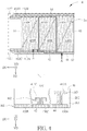
- FIG. 1 is a schematic diagram illustrating a top view of an electronic device according to a first embodiment of the present disclosure.
- the electronic device 1 includes a plurality of voltage traces 12, a plurality of region electrodes 30, and a voltage source module 16, in which an end of each voltage trace 12 may be individually electrically connected to the voltage source module 16, the other end of each voltage trace 12 may be electrically connected to one corresponding region electrode 30.
- the voltage traces 12 of this embodiment may be for example divided into voltage traces 12A-12F that are electrically insulated from each other, and the region electrodes 30 may also be for example divided into the region electrodes 30A-30F that are electrically insulated from each other.
- the voltage trace 12A is electrically connected to the corresponding region electrode 30A
- the voltage trace 12B is electrically connected to the corresponding region electrode 30B, and so on, but the present disclosure is not limited thereto.
- the voltage source module 16 may provide different driving voltages to different voltage traces 12A-12F
- each of the region electrodes 30A-30F corresponding to different voltage traces 12A-12F can receive a corresponding driving voltage, such that the driving voltages provided to the region electrodes 30A-30F can be independent of each other.
- the region electrodes 30A-30F may be electrodes located in different regions and separated from each other.
- the region electrodes 30A-30F may be for example the region electrodes in descending order of distance from the voltage source module 16. In some embodiments, widths of slits between the adjacent region electrodes 30A-30F are not limited to that shown in FIG. 1 .
- each of the region electrodes 30A-30F may receive a required driving voltage, for example, the region electrodes 30A-30F may receive the same or approximately the same driving voltage without being affected by different distances from voltage source module 16.
- the term "the same" driving voltage refers to as the driving voltage in a range from 98% of a predetermined value to less than 102% of the predetermined value, and the driving voltage outside the range is regarded as a "different" driving voltage.
- the equivalent resistance of the voltage trace 12F closer to the voltage source module 16 is less than the equivalent resistance of the voltage trace 12A farther from the voltage source module 16, and by means of providing the driving voltage to the voltage trace 12A greater than the driving voltage provided to the voltage trace 12F by the voltage source module 16, the driving voltage received by the region electrode 30A corresponding to the voltage trace 12A can be compensated to be approximate to or the same as the driving voltage received by the region electrode 30F corresponding to the voltage trace 12F.
- the region electrodes 30B-30E respectively corresponding to the voltage traces 12B-12E may receive the same or approximate driving voltage.
- the region electrodes 30A-30F can receive the same driving voltage.
- the driving voltages provided to the voltage traces 12A-12F by the voltage source module 16 may be for example a DC voltage, but not limited thereto.
- the voltage source module 16 may optionally have a plurality of voltage output terminals 16A1-16F1, and the voltage output terminal 16A1-16F1 are respectively electrically connected to the corresponding voltage traces 12A-12F for providing a plurality of independent and different driving voltages.
- the voltage source module 16 may be a single voltage source that is controlled and outputted by single one control device 18, but is not limited thereto.
- the voltage source module 16 may include at least two voltage source that are controlled and outputted by one or two or more control devices 18.
- the control device may be for example an integrated circuit.
- the electronic device may include a display device, an antenna device, a sensing device, a tiled device or other suitable non-display device.
- the antenna device may be for example a liquid crystal antenna, but is not limited thereto.
- the tiled device may be for example a tiled display device or a tiled antenna device, but is not limited thereto. It is noted that the electronic device may be any combination of the above-mentioned, but is not limited thereto.
- the following electronic device 1 being the display device is taken as an example for detailing the content of the present disclosure, but the present disclosure is not limited thereto.
- a top-view shape of the electronic device 1 is not limited to be rectangular and may be other geometric shapes.
- the electronic device 1 of this embodiment may have a display region 1a and a peripheral region 1b outside the display region 1a, but not limited thereto.
- the peripheral region 1b is disposed on a side S1 of the display region 1a facing a first direction D1.
- the peripheral region 1b may be disposed on a side of the display region 1a facing a direction different from the first direction D1, but not limited thereto.
- the electronic device 1 may include a plurality of sub-pixels 20 disposed in the display region 1a and for displaying images. For clarity, an enlarged diagram at right part of FIG. 1 exemplifies one of the sub-pixels 20, but the present disclosure is not limited thereto.
- the region electrodes 30A-30F are respectively disposed in different regions of the display region 1a and used for electrically connecting the sub-pixels 20 in different regions to different voltage traces 12A-12F. At least one sub-pixel 20 may be disposed in each region, i.e. each of the region electrodes 30A-30F may correspond to and be electrically connected to at least one sub-pixel 20. In this embodiment, each of the region electrodes 30A-30F may correspond to plural sub-pixels 20, for example, a whole of plural red sub-pixels, plural blue sub-pixels and plural green sub-pixels corresponding to the same one of the region electrode 30A-30F may be electrically connected to the one of the region electrode30A-30F.
- the sub-pixels 20 electrically connected to one of the region electrodes 30A-30F may receive a driving voltage from the corresponding one of the voltage trace 12A-12F.
- the sub-pixel 20-1 and the sub-pixel 20-1' may be electrically connected to the same voltage trace 12A and receive the same driving voltage.
- each sub-pixel 20 may include a light-emitting unit 22 for generating a brightness of a required gray level of the sub-pixel.
- the light-emitting unit 22 may include organic light-emitting diode or inorganic light-emitting diode (such as quantum dot light-emitting diode (such as QLED or QDLED), mini-LED, Micro-LED).
- the light-emitting unit 22 may optionally include fluorescent material, phosphor material or other suitable material or any combination thereof, but not limited thereto.
- three sub-pixels 20 capable of generating light of different colors may form a pixel PX, but not limited thereto.
- the formation of the pixel PX may be determined according to arrangement of the sub-pixels 22, such as array arrangement, PenTile arrangement, or other suitable arrangement.
- each sub-pixel 20 may further include a circuit 14 for electrically connecting a corresponding one of the region electrodes 30A-30F to the light-emitting unit 22 so as to driving the light-emitting unit 22.
- the circuit 14 may include a driving transistor 24 and a switch transistor 26, in which the driving transistor 24 is for controlling brightness of the light-emitting unit 22, a source(drain) electrode of the driving transistor 24 is electrically connected to an anode of the light-emitting unit 22, and a drain(source) electrode of the driving transistor 24 is electrically connected to the voltage source module 16.
- the switch transistor 26 is for controlling switch of the driving transistor 24, and a drain(source) electrode is electrically connected to a gate electrode of the driving transistor 24, but the present disclosure is not limited thereto.
- the electronic device 1 may further include a plurality of scan lines and a plurality of data lines for transferring signals for controlling the circuit 14. One of the scan lines is electrically connected to a gate electrode of one corresponding switch transistor 26, and one of the data lines is electrically connected to the a source(drain) of one corresponding switch transistor 26.
- the circuit 14 may not include the switch transistor 26, and the gate electrode of the driving transistor 24 is electrically connected to the corresponding data line.
- FIG. 1 ignores the scan lines and the data lines, but not limited thereto.
- the circuit 14 of the present disclosure is not limited to that as shown in FIG. 1 , and in some embodiments, the circuit 14 may further include other transistor, or the transistors in the circuit 14 may have other connection mode.
- light-emitting units 22 may be light-emitting diode package capable of generating light of different colors that are electrically connected to three circuits 14 respectively, but not limited thereto.
- each sub-pixel 20 may further include a pixel electrode (not shown in figures) for electrically connecting the circuit 14 to the light-emitting unit 22.
- the pixel electrode may be for example the anode or cathode of the light-emitting unit 22 or other suitable electrode. It is noted that the region electrode 30 is used for electrically connecting the circuit 14 to the voltage trace 12 and is different from the pixel electrode that is electrically connected between the circuit 14 and the light-emitting unit 22.
- the electronic device 1 may further include driving components or circuits for driving the sub-pixels and traces disposed in the peripheral region 1b.
- the driving components, traces and the voltage source module 16 in the peripheral region 1b may be bent toward back side of the display device (i.e. the back surface without displaying images), so as to improve a screen-to-body ratio of the display device.
- the region electrodes 30A-30F may be located within the regions in the display region 1a in the descending order of distance from the voltage source module 16, for example, the region electrodes 30A-30F are sequentially arranged along the first direction D1 from a side S2 to the side S1 of the display region 1a, but not limited thereto.
- the arranging direction of the region electrodes 30A-30F may be a second direction D2 or a direction different from the first direction D1 and the second direction D2.
- the voltage traces 12A-12F of this embodiment individually extend from the peripheral region 1b to the display region 1a and are electrically connected to different region electrodes 30A-30F respectively.
- the voltage trace 12 electrically connected to the farther region electrode 30 may cross and be electrically insulated from other region electrode 12, for example, the voltage trace 12A may cross the region electrodes 30B-30F that are not electrically connected to the voltage trace 12A.
- lengths of the voltage traces 12A-12F extending to different region electrodes 30A-30F may be different, resulting in difference between the equivalent resistances of the voltage traces 12A-12F.
- R P ⁇ L/(W ⁇ H)
- the equivalent resistances of the voltage traces 12A-12F may be calculated, where R is an equivalent resistance of a corresponding one of the voltage traces 12A-12F, P is resistivity of a corresponding one of the voltage traces 12A-12F, L is a length of the corresponding one of the voltage traces 12A-12F, such as an extending length of the corresponding one of the voltage traces 12A-12F measured when the voltage traces 12A-12F have the same sectional area in a top-view direction VD, W is a line width of the corresponding one of the voltage traces 12A-12F, such as a sectional width of the corresponding one of the voltage traces 12A-12F measured along a direction perpendicular to the extending direction and parallel to a horizontal direction, and H is a line height of the corresponding one of the voltage traces 12A-12F, such as a sectional height of the corresponding one of the voltage traces 12A-12F measured along the top-view direction
- the horizontal direction may be for example the first direction D1, the second direction D2 or a direction parallel to a plane formed by the first direction D1 and the second direction D2.
- the voltage traces 12A-12F have the same sheet resistance, i.e. the voltage traces 12A-12F have the same resistivity, the same line height and the same line width, the voltage traces 12A-12F will have different equivalent resistances that are sequentially decreased, but not limited thereto.
- the electronic device 1 may achieve uniform brightness.
- the voltage trace 12A electrically connected from the voltage source module 16 to the sub-pixel 20-1 is longer than the voltage trace 12F electrically connected from the voltage source module 16 to the sub-pixel 20-2.
- the equivalent resistance of the voltage trace 12A is greater than the equivalent resistance of the voltage trace 12F.
- the voltage source module 16 may provide a voltage V1 to the voltage trace 12A and provide a voltage V2 to the voltage trace 12F, in which the voltage V1 is greater than the voltage V2.
- the equivalent resistance of the voltage trace 12A is greater than the equivalent resistance of the voltage trace 12F, the same voltage finally received by the sub-pixels 20 electrically connected to the region electrode 30A and the region electrode 30F.
- the voltage V1 and the voltage V2 provided by the voltage source module 16 may be 9.0V and 7.5V, but not limited thereto.
- the final voltage received by the sub-pixel 20-1 and the sub-pixel 20-2 can be substantially the same, and uniformity of image brightness of the display device may be increased accordingly.
- the number of the voltage traces 12A-12F extending from the peripheral region 1b to the same one of the region electrodes 30A-30F may be two, but not limited thereto.
- the electronic device 1 includes two voltage traces 12A electrically connected to the sub-pixels 20 of the same one region electrode 30A, and so forth.
- the voltage source module 16 may further have a plurality of voltage output terminals 16A2-16F2, and the voltage output terminals electrically connected to the same one of the region electrodes 30A-30F provide the same driving voltage.
- each of the voltage output terminals 16A2-16F2 provide the same driving voltage as that provided by a corresponding one of the voltage output terminals 16A1-16F1.
- the number of the voltage trace of the voltage traces 12A-12F electrically connected to one of the region electrodes 30A-30F may be one or two or more.
- the voltage traces 12A-12F may respectively extend to two sides (right side and left side) of the region electrodes 30A-30F.
- the voltage traces 12A-12F may be disposed on the same side of the region electrodes 30A-30F, but not limited thereto.
- the region electrodes 30A far from the peripheral region 1b is not in contact with two sides S3, S4 of the display region 1a arranged in the second direction D2, and the region electrodes 30B-30F between the region electrode 30A and the peripheral region 1b may have concave side facing the peripheral region 1b, but the present disclosure is not limited thereto.
- the size (i.e. the number of the sub-pixel corresponding to one of the region electrodes 30A-30F) and shape of one of the region electrodes 30A-30F may be determined according to the required display device. In some embodiments, the sizes of the region electrodes 30A-30F are determined based on whether the brightness of the sub-pixels 20 in the same one of the region electrode 30A-30F can be recognized by human eyes, but not limited thereto.
- the region electrodes 30 shown in left portion of FIG. 1 are exemplified and are not shown as real shape. As shown in the enlarged diagram in right portion of FIG. 1 , the region electrodes 30 may for example include a plurality of strip electrodes, but not limited thereto. In some embodiments, the voltage traces 12A-12F may not extend into the display region 1a, but the region electrodes 30 extend to the outside of the display region 1a to be electrically connected to the voltage traces 12A-12F. In this embodiment, the electronic device 1 may further include a common voltage line 32 electrically connected to the cathodes of the light-emitting units 22 of all the sub-pixels 20.
- the electronic device of the present disclosure is not limited to the above embodiment, and other embodiments may exist.
- same components of other embodiments would be labeled with the same symbols of the first embodiment in the following description.
- the following description will detail the dissimilarities among different embodiments and the identical features will not be redundantly described.
- FIG. 2 is a schematic diagram illustrating a top view of a part of sub-pixels, a part of region electrodes and a part of voltage traces of an electronic device according to a second embodiment of the present disclosure.
- FIG. 2 only shows a part of the region electrodes, a part of the sub-pixels and a part of the voltage traces and ignores the voltage source module, but not limited thereto.
- a different between the electronic device 2 provided in this embodiment and the first embodiment shown in FIG. 1 is that the sub-pixels 20 electrically connected to the same one of the region electrodes 30A-30F and corresponding to different colors may be electrically connected to different voltage traces.
- the sub-pixels 20 may be divided into a plurality of sub-pixels 20R, a plurality of sub-pixels 20G, and a plurality of sub-pixels 20B, in which the light-emitting units 22 of the sub-pixels 20R, the light-emitting units 22 of the sub-pixel 20G and the light-emitting units 22 of the sub-pixel 20B may generate light of different colors, such as red, green and blue respectively, but not limited thereto.
- the region electrode 30A may include a region electrode 30AR, a region electrode 30AG, and a region electrode 30AB that are electrically insulated from each other.
- the region electrodes 30AR, 30AG, 30AB are electrically connected to the sub-pixels 20R, the sub-pixels 20G and the sub-pixels 20B respectively.
- the voltage trace 12A extending to the region electrode 30A may include a voltage trace 12AR, a voltage trace 12AG, and a voltage trace 12AB that are electrically insulated from each other, in which the voltage trace 12AR, the voltage trace 12AG, and the voltage trace 12AB are electrically connected to the region electrodes 30AR, 30AG, 30AB respectively.
- the sub-pixels 20R, the sub-pixels 20G, and the sub-pixels 20B may be electrically connected to the voltage source module through the voltage trace 12AR, the voltage trace 12AG and the voltage trace 12AB respectively.
- sub-pixels 20R, the sub-pixels 20G and the sub-pixels 20B located in the same region may receive individual driving voltages respectively.
- voltage output terminal of the voltage source module electrically connected to the voltage trace 12A may include three voltage output terminals electrically connected to the voltage trace 12AR, the voltage trace 12AG and the voltage trace 12AB respectively.
- the voltage trace 12A receiving the same one driving voltage may extend into a region corresponding to the region electrode 30A and be electrically connected to the voltage traces 12AR, 12AG, 12AB through corresponding circuits (not shown), such that the driving voltages may be divided into three driving voltages through the corresponding circuits (not shown), and the three driving voltages are provided to the voltage traces 12AR, 12AG, 12AB respectively. Accordingly, the sub-pixels 20R, the sub-pixels 20G and the sub-pixels 20B may receive different driving voltages.
- the arrangement of this embodiment can facilitate the sub-pixels 20R, 20G, 20B of different colors to be driven separately, thereby improving image quality of the display device.
- structures of other region electrodes may be the same as the structure of the region electrode 30A.
- FIG. 3 is a schematic diagram illustrating a top view of an electronic device according to a third embodiment of the present disclosure.
- FIG. 3 shows only the voltage traces and the region electrodes, but not limited thereto.
- the voltage traces 312A-312F and the region electrodes 330A-330F of the electronic device 3 provided in this embodiment may be formed of the same conductive layer M1.
- a difference between this embodiment and the above embodiment is that the voltage traces 312A-312F are located in the peripheral region 1b.
- At least one of the voltage traces 312A-312F may extend along surrounding of the display region 1a to the corresponding one of the region electrodes 330A-330F, for example, the voltage traces 312B, 312D extend along the side S4 to the corresponding region electrodes 330B, 330D.
- the region electrodes 330E, 330F close to the voltage source module are electrically connected to the voltage traces 312E, 312F on the side S1.
- the areas of different region electrodes 330A-330F may be equal, and shapes of different region electrodes 330A-330F are not limited to that shown in FIG. 3 and may be other shapes.
- the same one of the region electrodes 330A-330F is left-right asymmetrical, for example, the width of the region electrode 330A in the first direction D1 gradually increases along the second direction D2, and the region electrode 330A is electrically connected to the voltage trace 312A on the side S3 of the display region 1a; and the width of the adjacent region electrode 330B in the first direction D1 gradually increases along a direction opposite to the second direction D2, and the adjacent region electrode 330B is electrically connected to the voltage trace 312B on the side S4 of the display region 1a.
- Other region electrodes 330C, 330D may be varied based on the region electrode 330A and the adjacent region electrode 330B, but not limited thereto.
- the conductive layer M1 may include metal or other suitable material.
- the voltage traces 312A-312F and the region electrodes 330A-330F may be formed of different conductive layers but have the same arrangement as the third embodiment, in which different conductive layers may include the same material or different materials.
- a reference line D is drawn through a center of the side S1 and along the first direction D1 so as to extend across the region electrodes 330A-330F, and the reference points 330FP closest to the side S1 can be respectively found at the intersections of the reference points 330FP and the reference line D.
- the reference points 330FP are used to determine the distance between each of the region electrodes 330A-330F and the voltage source module 16, and the voltage source module 16 may provide the corresponding driving voltages according to the distances.
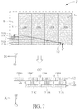
- FIG. 4 is a schematic diagram illustrating a sectional view and a top view of an electronic device according to a fourth embodiment of the present disclosure, in which a bottom portion of FIG. 4 schematically illustrates a sectional view of a top portion of FIG. 4 taken along a sectional line A-A'.
- FIG. 4 shows only the voltage traces and the region electrodes, but not limited thereto.
- a difference of the electronic device 4 provided in this embodiment and the third embodiment shown in FIG. 3 is that one of the voltage traces 412A-412F may at least partially overlap another one of the voltage traces 412A-412F in the top-view direction VD in this embodiment.
- the region electrodes 430A-430F and the voltage traces 412E, 412F may be formed of a conductive layer M1
- the voltage traces 412C, 412D may be formed of a conductive layer M2 on the conductive layer M1
- the voltage traces 412A, 412B may be formed of a conductive layer M3 on the conductive layer M2.
- an insulating layer IN1 is disposed between the conductive layer M1 and the conductive layer M2
- an insulating layer IN2 is disposed between the conductive layer M2 and the conductive layer M3.
- the voltage traces 412A, 412B may be formed of the conductive layer M2, and the voltage traces 412C, 412D may be formed of the conductive layer M3.
- the region electrodes 430A-430F may be formed of one of the conductive layer M2 and the conductive layer M3, the voltage traces 412C, 412D may be formed of another one of the conductive layer M1, the conductive layer M2 and the conductive layer M3 different from the conductive layer forming the region electrodes 430A-430F and the voltage traces 412E, 412F, and the voltage traces 412A, 412B may be formed of another one of the conductive layer M1, the conductive layer M2 and the conductive layer M3 different from the conductive layers forming the region electrodes 430A-430F and the voltage traces 412C, 412D, 412E, 412F.
- the insulating layer IN1 may have a plurality of contact holes 42, such that the voltage traces 412C, 412D may be electrically connected to the corresponding regions electrode 430C, 430D through the contact holes 42 respectively, and the insulating layer IN1 and the insulating layer IN2 may have a plurality of contact holes 44, such that the voltage traces 412A, 412B may be electrically connected to the corresponding region electrodes 430A, 430B through the contact holes 44 respectively.
- the electronic device 4 may further include a passivation layer 46 disposed on the insulating layer IN2 and the conductive layer M3.
- FIG. 5 is a schematic diagram illustrating a sectional view of an electronic device according to a fifth embodiment of the present disclosure, in which for clarity, FIG. 5 ignore the passivation, but not limited thereto.
- the voltage trace 512A may be formed of the conductive layer M1
- the region electrodes 530A, 530C, 530E may be formed of the conductive layer M3 in this embodiment, so the region electrode 530C extends into the contact hole 52 of the insulating layer IN2 to be connected to the voltage trace 512C
- the region electrode 530A extends into the contact hole 54 of the insulating layer IN1 and the insulating layer IN2 to be connected to the voltage trace 512A.
- other voltage traces and other the region electrodes may have the same structure as the region electrode 530A and the voltage trace 512A or the region electrode 530C and the voltage trace 512C and will not be redundantly detailed.
- FIG. 6 is a schematic diagram illustrating a top view and a sectional view of an electronic device according to a sixth embodiment of the present disclosure, in which a bottom portion of FIG. 6 schematically illustrates a sectional view of a top portion of FIG. 6 taken along a sectional line B-B'.
- FIG. 6 shows four voltage traces and four region electrodes, but the number of the voltage traces and the number of the region electrodes of the present disclosure are not limited thereto. Also, FIG. 6 ignores the passivation layer, but not limited thereto.
- a difference between the electronic device 6 and the third embodiment shown in FIG. 3 is that at least one of the voltage trace 612A-612D of this embodiment may overlap the display region 1a in the top-view direction VD.
- the region electrodes 630A-630D may be formed of the same conductive layer M1
- the voltage traces 612A-612C that are not electrically connected to the region electrode 630D may be formed of the same conductive layer M2
- the voltage trace 612D electrically connected to the region electrode 630D may be formed of the conductive layer M1, but not limited thereto.
- the voltage traces 612A-612C since the voltage traces 612A-612C are formed of the same conductive layer M2, the voltage traces 612A-612C may overlap the display region 1a in the top-view direction VD and be separated from each other, which means different voltage traces 612A-612C doesn't overlap each other.
- an insulating layer IN is disposed between the conductive layer M1 and the conductive layer M2 and has plural contact holes 62, such that each of the voltage traces 612A-612C may extend into corresponding one of the contact holes 62 to be electrically connected to the corresponding one of the region electrodes 630A-630C.
- the voltage trace 612D may be directly connected to the region electrode 630D. In some embodiments, the voltage trace 612D may overlap the display region 1a and be formed of the conductive layer M2.
- FIG. 7 is a schematic diagram illustrating a top view and a sectional view of an electronic device according to a seventh embodiment of the present disclosure, in which a bottom portion of FIG. 7 schematically illustrates a sectional view of a top portion of FIG. 7 taken along a sectional line C-C'.
- FIG. 7 shows only the voltage traces and the region electrodes and ignores the passivation layer, but not limited thereto.
- a difference between the electronic device 7 provided in this embodiment and the sixth embodiment shown in FIG. 6 is that the region electrodes 730A-730D and the voltage trace 712D are formed of the conductive layer M2, and the voltage traces 712A-712C are formed of the conductive layer M1 in this embodiment.
- the voltage traces 712A-712C of this embodiment extend into corresponding one of the contact holes 72 respectively to be electrically connected to corresponding one of the region electrodes 730A-730C.
- the voltage trace 712D may overlap the display region 1a and be formed of the conductive layer M1.
- FIG. 8 is a schematic diagram illustrating a top view and a sectional view of an electronic device according to an eighth embodiment of the present disclosure, in which a bottom portion of FIG. 8 schematically illustrates a sectional view of a top portion of FIG. 8 taken along a sectional line D-D'.
- FIG. 8 shows only the voltage traces and the region electrodes and ignores the passivation layer, but not limited thereto.
- a difference between the electronic device 8 provided in this embodiment and the sixth embodiment shown in FIG. 6 is that the voltage traces 812A-812C are formed of different conductive layers in this embodiment.
- the region electrodes 830A-830D and the voltage trace 812D may be formed of the same conductive layer M1, the voltage trace 812C may be formed of the conductive layer M2, the voltage trace 812B may be formed of the conductive layer M3, and the voltage trace 812A may be formed of the conductive layer M4.
- the voltage trace 812D may be directly connected to the region electrode 830D
- the voltage trace 812C may be electrically connected to the region electrode 830C through the contact hole 82 of the insulating layer IN1
- the voltage trace 812B may be electrically connected to the region electrode 830B through the contact hole 84 of the insulating layer IN1 and the insulating layer IN2
- the voltage trace 812A may be electrically connected to the region electrode 830A through the contact hole 86 of the insulating layer IN1, the insulating layer IN2 and the insulating layer IN3.
- FIG. 9 is a schematic diagram illustrating a top view and a sectional view of an electronic device according to a ninth embodiment of the present disclosure, in which a bottom portion of FIG. 9 schematically illustrates a sectional view of a top portion of FIG. 9 taken along a sectional line E-E'.
- FIG. 9 shows only the voltage traces and the region electrodes and ignores the passivation layer, but not limited thereto.
- a difference between the electronic device 9 provided in this embodiment and the eighth embodiment shown in FIG. 8 is that the region electrodes 930A-930D are formed of different conductive layers, and the voltage trace 912A-912D are formed of the same conductive in this embodiment.
- the region electrode 930D may be formed of the conductive layer M1
- the region electrode 930C may be formed of the conductive layer M2
- the region electrode 930B may be formed of the conductive layer M3
- the region electrode 930A may be formed of the conductive layer M4.
- the voltage traces 912A-912D may be formed of the conductive layer M4, so that the voltage trace 912A may be directly connected to the region electrode 930A, the voltage trace 912B may be electrically connected to the region electrode 930B through the contact hole 92 of the insulating layer IN3, the voltage trace 912C may be electrically connected to the region electrode 930C through the contact hole 94 of the insulating layer IN3 and the insulating layer IN2, and the voltage trace 912D may be electrically connected to the region electrode 930D through the contact hole 96 of the insulating layer IN3, the insulating layer IN2 and the insulating layer IN1.
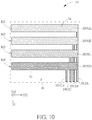
- FIG. 10 is a schematic diagram illustrating a top view of an electronic device according to a tenth embodiment of the present disclosure.
- FIG. 10 shows only the voltage traces and the region electrodes, but not limited thereto.
- a difference between the electronic device 10 provided in this embodiment and the sixth embodiment shown in FIG. 6 is that the region electrodes 1030A-1030D are formed of different conductive layers, and each of the voltage traces 1012A-1012D and a corresponding one of the region electrodes 1030A-1030D are formed of the same conductive layer.
- the region electrode 1030A and the voltage trace 1012A are formed of the conductive layer M1
- the region electrode 1030B and the voltage trace 1012B are formed of the conductive layer M2
- the region electrode 1030C and the voltage trace 1012C are formed of the conductive layer M3
- the region electrode 1030D and the voltage trace 1012D are formed of the conductive layer M4.
- the driving voltage received by the region electrode farther from the voltage source module can be compensated to be close to or equal to the driving voltage received by the region electrode closer to the voltage source module by providing different driving voltages to different voltage traces. Accordingly, the sub-pixels in different regions may be operated under the same driving voltage, thereby improving uniformity of image brightness of the electronic device.
Landscapes
- Engineering & Computer Science (AREA)
- Physics & Mathematics (AREA)
- Computer Hardware Design (AREA)
- General Physics & Mathematics (AREA)
- Theoretical Computer Science (AREA)
- Microelectronics & Electronic Packaging (AREA)
- Devices For Indicating Variable Information By Combining Individual Elements (AREA)
- Electroluminescent Light Sources (AREA)
Abstract
Description
- The present disclosure relates to an electronic device according to the pre-characterizing clauses of
claim 1, and more particularly to an electronic device providing different voltages to different region electrodes. - In self-emissive display devices, a light-emitting component in each sub-pixel is directly used to display brightness level (gray level), so the self-emissive display device can have advantages of high contrast, wide viewing angle, short response time and light weight as compared with non-self-emissive display devices, such that the self-emissive display device can replace the non-self-emissive display device in some applications and become mainstream. In the self-emissive display device, since the required image is displayed by controlling the brightness level of each light-emitting component, driving voltage provided to each sub-pixel will affect the brightness of the light-emitting component.
- In conventional self-emissive display device, to drive the light-emitting component of each sub-pixel, each sub-pixel is electrically connected to the same voltage source by a corresponding voltage trace. However, with the difference in the distances between the sub-pixels and the voltage source, the equivalent resistances of the voltage traces are different. For this reason, when the voltage source provides the same driving voltage to the voltage traces, the sub-pixels electrically connected to the voltage traces with different equivalent resistances will receive different driving voltages, resulting in inconsistency of image brightness of the display device.
- This in mind, the present disclosure aims at providing an electronic device that provides different driving voltages to different voltage traces to improve uniformity of image brightness.
- This is achieved by an electronic device with different voltage traces provided with different driving voltages according to the claims. The dependent claims pertain to corresponding further developments and improvements.
- As will be seen more clearly from the detailed description following below, an electronic device is provided by the present disclosure. The electronic device includes a first voltage trace, a second voltage trace, a first region electrode, a second region electrode, and a voltage source module. The second voltage trace is electrically insulated from the first voltage trace, the first region electrode is electrically connected to the first voltage trace, and the second region electrode is electrically connected to the second voltage trace. The voltage source module provides a first driving voltage to the first voltage trace and provides a second driving voltage to the second voltage trace, in which the first driving voltage is different from the second driving voltage.
- These and other objectives of the present disclosure will no doubt become obvious to those of ordinary skill in the art after reading the following detailed description of the embodiment that is illustrated in the various figures and drawings.
- In the following, the disclosure is further illustrated by way of example, taking reference to the accompanying drawings. Thereof:
-
FIG. 1 is a schematic diagram illustrating a top view of an electronic device according to a first embodiment of the present disclosure; -
FIG. 2 is a schematic diagram illustrating a top view of a part of sub-pixels, a part of region electrodes and a part of voltage traces of an electronic device according to a second embodiment of the present disclosure; -
FIG. 3 is a schematic diagram illustrating a top view of an electronic device according to a third embodiment of the present disclosure; -
FIG. 4 is a schematic diagram illustrating a sectional view and a top view of an electronic device according to a fourth embodiment of the present disclosure; -
FIG. 5 is a schematic diagram illustrating a sectional view of an electronic device according to a fifth embodiment of the present disclosure; -
FIG. 6 is a schematic diagram illustrating a top view and a sectional view of an electronic device according to a sixth embodiment of the present disclosure; -
FIG. 7 is a schematic diagram illustrating a top view and a sectional view of an electronic device according to a seventh embodiment of the present disclosure; -
FIG. 8 is a schematic diagram illustrating a top view and a sectional view of an electronic device according to an eighth embodiment of the present disclosure; -
FIG. 9 is a schematic diagram illustrating a top view and a sectional view of an electronic device according to a ninth embodiment of the present disclosure; and -
FIG. 10 is a schematic diagram illustrating a top view of an electronic device according to a tenth embodiment of the present disclosure. - The present disclosure may be understood by reference to the following detailed description, taken in conjunction with the drawings as described below. It is noted that, for purposes of illustrative clarity and being easily understood by the readers, various drawings of this disclosure show a portion of the electronic device, and certain components in various drawings may not be drawn to scale. In addition, the number and dimension of each component shown in drawings are only illustrative and are not intended to limit the scope of the present disclosure.
- Certain terms are used throughout the description and following claims to refer to particular components. As one skilled in the art will understand, electronic equipment manufacturers may refer to a component by different names. This document does not intend to distinguish between components that differ in name but not function. In the following description and in the claims, the terms "include", "comprise" and "have" are used in an open-ended fashion, and thus should be interpreted to mean "include, but not limited to...".
- It will be understood that when a component is referred to as being "connected to" another component (or its variant), it can be directly connected to the another component, or connected to the another component through one or more intervening components.
- Spatially relative terms, such as "above", "on", "beneath", "below", "under", "left", "right", "before", "front", "after", "behind" and the like, used in the following embodiments only refer to the directions in the drawings and are not intended to limit the present disclosure. It should be understood that the components in the drawings may be disposed in any kind of formation known by one skilled in the related art to describe the components in a certain way. Furthermore, when one layer is "on" another layer or a substrate, it can be "directly on" the another layer or the substrate, or the one layer is on the another layer or the substrate, or another layer may be sandwiched between the one layer and the another layer or the substrate.
- In addition, in this specification, relative expressions, such as "lower", "bottom", "upper" or "top", may be used to describe the position of one component relative to another. It is understood that if the device in the figures is turned over, components described as "lower" would then be oriented to be "upper" components.
- Although the terms such as first, second, etc. may be used in the description and following claims to describe various components in claims, these terms doesn't mean or represent the claimed components have order and doesn't represent the order of one claimed component and another one claimed component, or the sequence in manufacturing method. These terms are used to discriminate a claimed component with a denomination from another one claimed component with the same denomination.
- It should be noted that the technical features in different embodiments described in the following can be replaced, recombined, or mixed with one another to constitute another embodiment without departing from the spirit of the present disclosure.
-
FIG. 1 is a schematic diagram illustrating a top view of an electronic device according to a first embodiment of the present disclosure. Theelectronic device 1 includes a plurality ofvoltage traces 12, a plurality ofregion electrodes 30, and avoltage source module 16, in which an end of eachvoltage trace 12 may be individually electrically connected to thevoltage source module 16, the other end of eachvoltage trace 12 may be electrically connected to onecorresponding region electrode 30. The voltage traces 12 of this embodiment may be for example divided intovoltage traces 12A-12F that are electrically insulated from each other, and theregion electrodes 30 may also be for example divided into theregion electrodes 30A-30F that are electrically insulated from each other. As an example, thevoltage trace 12A is electrically connected to thecorresponding region electrode 30A, thevoltage trace 12B is electrically connected to thecorresponding region electrode 30B, and so on, but the present disclosure is not limited thereto. Since thevoltage source module 16 may provide different driving voltages todifferent voltage traces 12A-12F, each of theregion electrodes 30A-30F corresponding todifferent voltage traces 12A-12F can receive a corresponding driving voltage, such that the driving voltages provided to theregion electrodes 30A-30F can be independent of each other. Theregion electrodes 30A-30F may be electrodes located in different regions and separated from each other. Theregion electrodes 30A-30F may be for example the region electrodes in descending order of distance from thevoltage source module 16. In some embodiments, widths of slits between theadjacent region electrodes 30A-30F are not limited to that shown inFIG. 1 . - For example, when equivalent resistances of the voltage traces 12A-12F are not the same, by means of providing different and independent driving voltages to
different voltage traces 12A-12F, each of theregion electrodes 30A-30F may receive a required driving voltage, for example, theregion electrodes 30A-30F may receive the same or approximately the same driving voltage without being affected by different distances fromvoltage source module 16. As used herein, the term "the same" driving voltage refers to as the driving voltage in a range from 98% of a predetermined value to less than 102% of the predetermined value, and the driving voltage outside the range is regarded as a "different" driving voltage. Taking thevoltage traces 12A-12F being respectively electrically connected to theregion electrodes 30 in descending order of distance from thevoltage source module 16 as an example, the equivalent resistance of thevoltage trace 12F closer to thevoltage source module 16 is less than the equivalent resistance of thevoltage trace 12A farther from thevoltage source module 16, and by means of providing the driving voltage to thevoltage trace 12A greater than the driving voltage provided to thevoltage trace 12F by thevoltage source module 16, the driving voltage received by theregion electrode 30A corresponding to thevoltage trace 12A can be compensated to be approximate to or the same as the driving voltage received by theregion electrode 30F corresponding to thevoltage trace 12F. For the same reason, theregion electrodes 30B-30E respectively corresponding to thevoltage traces 12B-12E may receive the same or approximate driving voltage. Therefore, no matter what distance between theregion electrodes 30A-30F and thevoltage source module 16 is, theregion electrodes 30A-30F can receive the same driving voltage. In this embodiment, the driving voltages provided to thevoltage traces 12A-12F by thevoltage source module 16 may be for example a DC voltage, but not limited thereto. - The
voltage source module 16 may optionally have a plurality of voltage output terminals 16A1-16F1, and the voltage output terminal 16A1-16F1 are respectively electrically connected to thecorresponding voltage traces 12A-12F for providing a plurality of independent and different driving voltages. In this embodiment, thevoltage source module 16 may be a single voltage source that is controlled and outputted by single onecontrol device 18, but is not limited thereto. In some embodiments, thevoltage source module 16 may include at least two voltage source that are controlled and outputted by one or two ormore control devices 18. In some embodiments, the control device may be for example an integrated circuit. - The electronic device may include a display device, an antenna device, a sensing device, a tiled device or other suitable non-display device. The antenna device may be for example a liquid crystal antenna, but is not limited thereto. The tiled device may be for example a tiled display device or a tiled antenna device, but is not limited thereto. It is noted that the electronic device may be any combination of the above-mentioned, but is not limited thereto. The following
electronic device 1 being the display device is taken as an example for detailing the content of the present disclosure, but the present disclosure is not limited thereto. In some embodiments, a top-view shape of theelectronic device 1 is not limited to be rectangular and may be other geometric shapes. - As shown in
FIG. 1 , theelectronic device 1 of this embodiment may have a display region 1a and aperipheral region 1b outside the display region 1a, but not limited thereto. In this embodiment, theperipheral region 1b is disposed on a side S1 of the display region 1a facing a first direction D1. In some embodiments, theperipheral region 1b may be disposed on a side of the display region 1a facing a direction different from the first direction D1, but not limited thereto. Theelectronic device 1 may include a plurality of sub-pixels 20 disposed in the display region 1a and for displaying images. For clarity, an enlarged diagram at right part ofFIG. 1 exemplifies one of the sub-pixels 20, but the present disclosure is not limited thereto. Theregion electrodes 30A-30F are respectively disposed in different regions of the display region 1a and used for electrically connecting the sub-pixels 20 in different regions to different voltage traces 12A-12F. At least one sub-pixel 20 may be disposed in each region, i.e. each of theregion electrodes 30A-30F may correspond to and be electrically connected to at least onesub-pixel 20. In this embodiment, each of theregion electrodes 30A-30F may correspond to plural sub-pixels 20, for example, a whole of plural red sub-pixels, plural blue sub-pixels and plural green sub-pixels corresponding to the same one of theregion electrode 30A-30F may be electrically connected to the one of the region electrode30A-30F. In other words, the sub-pixels 20 electrically connected to one of theregion electrodes 30A-30F may receive a driving voltage from the corresponding one of thevoltage trace 12A-12F. For example, the sub-pixel 20-1 and the sub-pixel 20-1' may be electrically connected to thesame voltage trace 12A and receive the same driving voltage. - Taking a self-emissive display device as an example, each sub-pixel 20 may include a light-emitting
unit 22 for generating a brightness of a required gray level of the sub-pixel. In some embodiments, the light-emittingunit 22 may include organic light-emitting diode or inorganic light-emitting diode (such as quantum dot light-emitting diode (such as QLED or QDLED), mini-LED, Micro-LED). The light-emittingunit 22 may optionally include fluorescent material, phosphor material or other suitable material or any combination thereof, but not limited thereto. In this embodiment, three sub-pixels 20 capable of generating light of different colors may form a pixel PX, but not limited thereto. In some embodiments, the formation of the pixel PX may be determined according to arrangement of the sub-pixels 22, such as array arrangement, PenTile arrangement, or other suitable arrangement. - In some embodiments, each sub-pixel 20 may further include a
circuit 14 for electrically connecting a corresponding one of theregion electrodes 30A-30F to the light-emittingunit 22 so as to driving the light-emittingunit 22. For example, thecircuit 14 may include a drivingtransistor 24 and aswitch transistor 26, in which the drivingtransistor 24 is for controlling brightness of the light-emittingunit 22, a source(drain) electrode of the drivingtransistor 24 is electrically connected to an anode of the light-emittingunit 22, and a drain(source) electrode of the drivingtransistor 24 is electrically connected to thevoltage source module 16. Theswitch transistor 26 is for controlling switch of the drivingtransistor 24, and a drain(source) electrode is electrically connected to a gate electrode of the drivingtransistor 24, but the present disclosure is not limited thereto. Furthermore, theelectronic device 1 may further include a plurality of scan lines and a plurality of data lines for transferring signals for controlling thecircuit 14. One of the scan lines is electrically connected to a gate electrode of one correspondingswitch transistor 26, and one of the data lines is electrically connected to the a source(drain) of one correspondingswitch transistor 26. In some embodiments, thecircuit 14 may not include theswitch transistor 26, and the gate electrode of the drivingtransistor 24 is electrically connected to the corresponding data line. For clearly illustrating theelectronic device 1 of this embodiment,FIG. 1 ignores the scan lines and the data lines, but not limited thereto. Thecircuit 14 of the present disclosure is not limited to that as shown inFIG. 1 , and in some embodiments, thecircuit 14 may further include other transistor, or the transistors in thecircuit 14 may have other connection mode. In some embodiments, light-emittingunits 22 may be light-emitting diode package capable of generating light of different colors that are electrically connected to threecircuits 14 respectively, but not limited thereto. In some embodiments, each sub-pixel 20 may further include a pixel electrode (not shown in figures) for electrically connecting thecircuit 14 to the light-emittingunit 22. In some embodiments, the pixel electrode may be for example the anode or cathode of the light-emittingunit 22 or other suitable electrode. It is noted that theregion electrode 30 is used for electrically connecting thecircuit 14 to thevoltage trace 12 and is different from the pixel electrode that is electrically connected between thecircuit 14 and the light-emittingunit 22. - In some embodiments, the
electronic device 1 may further include driving components or circuits for driving the sub-pixels and traces disposed in theperipheral region 1b. In some embodiments, the driving components, traces and thevoltage source module 16 in theperipheral region 1b may be bent toward back side of the display device (i.e. the back surface without displaying images), so as to improve a screen-to-body ratio of the display device. - In this embodiment, the
region electrodes 30A-30F may be located within the regions in the display region 1a in the descending order of distance from thevoltage source module 16, for example, theregion electrodes 30A-30F are sequentially arranged along the first direction D1 from a side S2 to the side S1 of the display region 1a, but not limited thereto. The arranging direction of theregion electrodes 30A-30F may be a second direction D2 or a direction different from the first direction D1 and the second direction D2. The voltage traces 12A-12F of this embodiment individually extend from theperipheral region 1b to the display region 1a and are electrically connected todifferent region electrodes 30A-30F respectively. When one of theregion electrodes 30 is not the electrode closest to theperipheral region 1b, thevoltage trace 12 electrically connected to thefarther region electrode 30 may cross and be electrically insulated fromother region electrode 12, for example, thevoltage trace 12A may cross theregion electrodes 30B-30F that are not electrically connected to thevoltage trace 12A. Hence, lengths of the voltage traces 12A-12F extending todifferent region electrodes 30A-30F may be different, resulting in difference between the equivalent resistances of the voltage traces 12A-12F. - Based on formula (1): R=P×L/(W×H), the equivalent resistances of the voltage traces 12A-12F may be calculated, where R is an equivalent resistance of a corresponding one of the voltage traces 12A-12F, P is resistivity of a corresponding one of the voltage traces 12A-12F, L is a length of the corresponding one of the voltage traces 12A-12F, such as an extending length of the corresponding one of the voltage traces 12A-12F measured when the voltage traces 12A-12F have the same sectional area in a top-view direction VD, W is a line width of the corresponding one of the voltage traces 12A-12F, such as a sectional width of the corresponding one of the voltage traces 12A-12F measured along a direction perpendicular to the extending direction and parallel to a horizontal direction, and H is a line height of the corresponding one of the voltage traces 12A-12F, such as a sectional height of the corresponding one of the voltage traces 12A-12F measured along the top-view direction VD. The horizontal direction may be for example the first direction D1, the second direction D2 or a direction parallel to a plane formed by the first direction D1 and the second direction D2. For example, when the voltage traces 12A-12F have the same sheet resistance, i.e. the voltage traces 12A-12F have the same resistivity, the same line height and the same line width, the voltage traces 12A-12F will have different equivalent resistances that are sequentially decreased, but not limited thereto. It is noted that, by means of providing different driving voltages to different voltage traces 12A-12F by the
voltage source module 16, for example, providing the driving voltages from high to low in order to the voltage traces 12A-12F with equivalent resistances from high to low in sequence, the driving voltage received by the sub-pixel 20, such as the sub-pixel 20-1 or 20-1', farther from thevoltage source module 16 is appropriately compensated to be the same as or approximately the same as the driving voltage received by the sub-pixel 20, such as the sub-pixel 20-2, closer to thevoltage source module 16, thereby mitigating the issue of different driving voltages received by the sub-pixels 20 due to different distances between the sub-pixels 20 and thevoltage source module 16. Accordingly, theelectronic device 1 may achieve uniform brightness. - It is noted that in this embodiment, since the sub-pixel 20-1 electrically connected to the
region electrode 30A is farther from thevoltage source module 16 than the sub-pixel 20-2 electrically connected to theregion electrode 30F, thevoltage trace 12A electrically connected from thevoltage source module 16 to the sub-pixel 20-1 is longer than thevoltage trace 12F electrically connected from thevoltage source module 16 to the sub-pixel 20-2. When the voltage traces 12A, 12F have the same sheet resistance, the equivalent resistance of thevoltage trace 12A is greater than the equivalent resistance of thevoltage trace 12F. As an example, thevoltage source module 16 may provide a voltage V1 to thevoltage trace 12A and provide a voltage V2 to thevoltage trace 12F, in which the voltage V1 is greater than the voltage V2. Because the equivalent resistance of thevoltage trace 12A is greater than the equivalent resistance of thevoltage trace 12F, the same voltage finally received by the sub-pixels 20 electrically connected to theregion electrode 30A and theregion electrode 30F. For example, when all the sub-pixels 20 of theelectronic device 1 is predetermined to receive a voltage, such as 7V, the voltage V1 and the voltage V2 provided by thevoltage source module 16 may be 9.0V and 7.5V, but not limited thereto. Through providing different driving voltages VI, V2 to thevoltage trace 12A and thevoltage trace 12F, the final voltage received by the sub-pixel 20-1 and the sub-pixel 20-2 can be substantially the same, and uniformity of image brightness of the display device may be increased accordingly. - In this embodiment, the number of the voltage traces 12A-12F extending from the
peripheral region 1b to the same one of theregion electrodes 30A-30F may be two, but not limited thereto. For example, theelectronic device 1 includes twovoltage traces 12A electrically connected to the sub-pixels 20 of the same oneregion electrode 30A, and so forth. In such situation, thevoltage source module 16 may further have a plurality of voltage output terminals 16A2-16F2, and the voltage output terminals electrically connected to the same one of theregion electrodes 30A-30F provide the same driving voltage. In this embodiment, each of the voltage output terminals 16A2-16F2 provide the same driving voltage as that provided by a corresponding one of the voltage output terminals 16A1-16F1. In some embodiments, the number of the voltage trace of the voltage traces 12A-12F electrically connected to one of theregion electrodes 30A-30F may be one or two or more. In this embodiment, the voltage traces 12A-12F may respectively extend to two sides (right side and left side) of theregion electrodes 30A-30F. In other embodiments, the voltage traces 12A-12F may be disposed on the same side of theregion electrodes 30A-30F, but not limited thereto. It is noted that, in this embodiment, theregion electrodes 30A far from theperipheral region 1b is not in contact with two sides S3, S4 of the display region 1a arranged in the second direction D2, and theregion electrodes 30B-30F between theregion electrode 30A and theperipheral region 1b may have concave side facing theperipheral region 1b, but the present disclosure is not limited thereto. The size (i.e. the number of the sub-pixel corresponding to one of theregion electrodes 30A-30F) and shape of one of theregion electrodes 30A-30F may be determined according to the required display device. In some embodiments, the sizes of theregion electrodes 30A-30F are determined based on whether the brightness of the sub-pixels 20 in the same one of theregion electrode 30A-30F can be recognized by human eyes, but not limited thereto. - The
region electrodes 30 shown in left portion ofFIG. 1 are exemplified and are not shown as real shape. As shown in the enlarged diagram in right portion ofFIG. 1 , theregion electrodes 30 may for example include a plurality of strip electrodes, but not limited thereto. In some embodiments, the voltage traces 12A-12F may not extend into the display region 1a, but theregion electrodes 30 extend to the outside of the display region 1a to be electrically connected to the voltage traces 12A-12F. In this embodiment, theelectronic device 1 may further include acommon voltage line 32 electrically connected to the cathodes of the light-emittingunits 22 of all the sub-pixels 20. - The electronic device of the present disclosure is not limited to the above embodiment, and other embodiments may exist. For simplicity, same components of other embodiments would be labeled with the same symbols of the first embodiment in the following description. To compare the embodiments conveniently, the following description will detail the dissimilarities among different embodiments and the identical features will not be redundantly described.
-
FIG. 2 is a schematic diagram illustrating a top view of a part of sub-pixels, a part of region electrodes and a part of voltage traces of an electronic device according to a second embodiment of the present disclosure. For clarity,FIG. 2 only shows a part of the region electrodes, a part of the sub-pixels and a part of the voltage traces and ignores the voltage source module, but not limited thereto. A different between theelectronic device 2 provided in this embodiment and the first embodiment shown inFIG. 1 is that the sub-pixels 20 electrically connected to the same one of theregion electrodes 30A-30F and corresponding to different colors may be electrically connected to different voltage traces. Taking theregion electrode 30A as an example, the sub-pixels 20 may be divided into a plurality of sub-pixels 20R, a plurality of sub-pixels 20G, and a plurality of sub-pixels 20B, in which the light-emittingunits 22 of the sub-pixels 20R, the light-emittingunits 22 of the sub-pixel 20G and the light-emittingunits 22 of the sub-pixel 20B may generate light of different colors, such as red, green and blue respectively, but not limited thereto. Theregion electrode 30A may include a region electrode 30AR, a region electrode 30AG, and a region electrode 30AB that are electrically insulated from each other. The region electrodes 30AR, 30AG, 30AB are electrically connected to the sub-pixels 20R, the sub-pixels 20G and the sub-pixels 20B respectively. In addition, thevoltage trace 12A extending to theregion electrode 30A may include a voltage trace 12AR, a voltage trace 12AG, and a voltage trace 12AB that are electrically insulated from each other, in which the voltage trace 12AR, the voltage trace 12AG, and the voltage trace 12AB are electrically connected to the region electrodes 30AR, 30AG, 30AB respectively. For this reason, the sub-pixels 20R, the sub-pixels 20G, and the sub-pixels 20B may be electrically connected to the voltage source module through the voltage trace 12AR, the voltage trace 12AG and the voltage trace 12AB respectively. That is to say that the sub-pixels 20R, the sub-pixels 20G and the sub-pixels 20B located in the same region (corresponding to thesame region electrode 30A) may receive individual driving voltages respectively. For example, voltage output terminal of the voltage source module electrically connected to thevoltage trace 12A may include three voltage output terminals electrically connected to the voltage trace 12AR, the voltage trace 12AG and the voltage trace 12AB respectively. In some embodiments, thevoltage trace 12A receiving the same one driving voltage may extend into a region corresponding to theregion electrode 30A and be electrically connected to the voltage traces 12AR, 12AG, 12AB through corresponding circuits (not shown), such that the driving voltages may be divided into three driving voltages through the corresponding circuits (not shown), and the three driving voltages are provided to the voltage traces 12AR, 12AG, 12AB respectively. Accordingly, the sub-pixels 20R, the sub-pixels 20G and the sub-pixels 20B may receive different driving voltages. When the light-emittingunits 22 of the sub-pixels 20R, the light-emittingunits 22 of the sub-pixels 20G and the light-emittingunits 22 of the sub-pixels 20B need different driving voltages, the arrangement of this embodiment can facilitate the sub-pixels 20R, 20G, 20B of different colors to be driven separately, thereby improving image quality of the display device. In some embodiments, structures of other region electrodes may be the same as the structure of theregion electrode 30A. -
FIG. 3 is a schematic diagram illustrating a top view of an electronic device according to a third embodiment of the present disclosure. For clarity,FIG. 3 shows only the voltage traces and the region electrodes, but not limited thereto. The voltage traces 312A-312F and theregion electrodes 330A-330F of theelectronic device 3 provided in this embodiment may be formed of the same conductive layer M1. A difference between this embodiment and the above embodiment is that the voltage traces 312A-312F are located in theperipheral region 1b. In this embodiment, at least one of the voltage traces 312A-312F may extend along surrounding of the display region 1a to the corresponding one of theregion electrodes 330A-330F, for example, the voltage traces 312B, 312D extend along the side S4 to thecorresponding region electrodes region electrodes different region electrodes 330A-330F may be equal, and shapes ofdifferent region electrodes 330A-330F are not limited to that shown inFIG. 3 and may be other shapes. In this embodiment, the same one of theregion electrodes 330A-330F is left-right asymmetrical, for example, the width of theregion electrode 330A in the first direction D1 gradually increases along the second direction D2, and theregion electrode 330A is electrically connected to thevoltage trace 312A on the side S3 of the display region 1a; and the width of theadjacent region electrode 330B in the first direction D1 gradually increases along a direction opposite to the second direction D2, and theadjacent region electrode 330B is electrically connected to thevoltage trace 312B on the side S4 of the display region 1a.Other region electrodes region electrode 330A and theadjacent region electrode 330B, but not limited thereto. In some embodiments, the conductive layer M1 may include metal or other suitable material. In some embodiments, the voltage traces 312A-312F and theregion electrodes 330A-330F may be formed of different conductive layers but have the same arrangement as the third embodiment, in which different conductive layers may include the same material or different materials. - In addition, in this embodiment, when the
voltage source module 16 is close to the side S1, a reference line D is drawn through a center of the side S1 and along the first direction D1 so as to extend across theregion electrodes 330A-330F, and the reference points 330FP closest to the side S1 can be respectively found at the intersections of the reference points 330FP and the reference line D. The reference points 330FP are used to determine the distance between each of theregion electrodes 330A-330F and thevoltage source module 16, and thevoltage source module 16 may provide the corresponding driving voltages according to the distances. -
FIG. 4 is a schematic diagram illustrating a sectional view and a top view of an electronic device according to a fourth embodiment of the present disclosure, in which a bottom portion ofFIG. 4 schematically illustrates a sectional view of a top portion ofFIG. 4 taken along a sectional line A-A'. For clarity,FIG. 4 shows only the voltage traces and the region electrodes, but not limited thereto. A difference of theelectronic device 4 provided in this embodiment and the third embodiment shown inFIG. 3 is that one of the voltage traces 412A-412F may at least partially overlap another one of the voltage traces 412A-412F in the top-view direction VD in this embodiment. Specifically, at least two of the voltage traces 412A-412F overlapping each other in the top-view direction VD may be formed of different conductive layers. For example, theregion electrodes 430A-430F and the voltage traces 412E, 412F may be formed of a conductive layer M1, the voltage traces 412C, 412D may be formed of a conductive layer M2 on the conductive layer M1, and the voltage traces 412A, 412B may be formed of a conductive layer M3 on the conductive layer M2. Also, an insulating layer IN1 is disposed between the conductive layer M1 and the conductive layer M2, and an insulating layer IN2 is disposed between the conductive layer M2 and the conductive layer M3. In some embodiments, the voltage traces 412A, 412B may be formed of the conductive layer M2, and the voltage traces 412C, 412D may be formed of the conductive layer M3. In some embodiments, theregion electrodes 430A-430F may be formed of one of the conductive layer M2 and the conductive layer M3, the voltage traces 412C, 412D may be formed of another one of the conductive layer M1, the conductive layer M2 and the conductive layer M3 different from the conductive layer forming theregion electrodes 430A-430F and the voltage traces 412E, 412F, and the voltage traces 412A, 412B may be formed of another one of the conductive layer M1, the conductive layer M2 and the conductive layer M3 different from the conductive layers forming theregion electrodes 430A-430F and the voltage traces 412C, 412D, 412E, 412F. - The insulating layer IN1 may have a plurality of contact holes 42, such that the voltage traces 412C, 412D may be electrically connected to the corresponding regions electrode 430C, 430D through the contact holes 42 respectively, and the insulating layer IN1 and the insulating layer IN2 may have a plurality of contact holes 44, such that the voltage traces 412A, 412B may be electrically connected to the
corresponding region electrodes peripheral region 1b located outside the display region 1a can be shrunk, thereby reduce border width of theelectronic device 4. In some embodiments, theelectronic device 4 may further include apassivation layer 46 disposed on the insulating layer IN2 and the conductive layer M3. -
FIG. 5 is a schematic diagram illustrating a sectional view of an electronic device according to a fifth embodiment of the present disclosure, in which for clarity,FIG. 5 ignore the passivation, but not limited thereto. A difference between theelectronic device 5 provided in this embodiment and the fourth embodiment shown inFIG. 4 is that thevoltage trace 512A may be formed of the conductive layer M1, and theregion electrodes region electrode 530C extends into thecontact hole 52 of the insulating layer IN2 to be connected to thevoltage trace 512C, and theregion electrode 530A extends into thecontact hole 54 of the insulating layer IN1 and the insulating layer IN2 to be connected to thevoltage trace 512A. In some embodiments, other voltage traces and other the region electrodes may have the same structure as theregion electrode 530A and thevoltage trace 512A or theregion electrode 530C and thevoltage trace 512C and will not be redundantly detailed. -
FIG. 6 is a schematic diagram illustrating a top view and a sectional view of an electronic device according to a sixth embodiment of the present disclosure, in which a bottom portion ofFIG. 6 schematically illustrates a sectional view of a top portion ofFIG. 6 taken along a sectional line B-B'. For clarity,FIG. 6 shows four voltage traces and four region electrodes, but the number of the voltage traces and the number of the region electrodes of the present disclosure are not limited thereto. Also,FIG. 6 ignores the passivation layer, but not limited thereto. A difference between theelectronic device 6 and the third embodiment shown inFIG. 3 is that at least one of thevoltage trace 612A-612D of this embodiment may overlap the display region 1a in the top-view direction VD. Specifically, theregion electrodes 630A-630D may be formed of the same conductive layer M1, the voltage traces 612A-612C that are not electrically connected to theregion electrode 630D may be formed of the same conductive layer M2, and thevoltage trace 612D electrically connected to theregion electrode 630D may be formed of the conductive layer M1, but not limited thereto. In this embodiment, since the voltage traces 612A-612C are formed of the same conductive layer M2, the voltage traces 612A-612C may overlap the display region 1a in the top-view direction VD and be separated from each other, which means different voltage traces 612A-612C doesn't overlap each other. In addition, an insulating layer IN is disposed between the conductive layer M1 and the conductive layer M2 and has plural contact holes 62, such that each of the voltage traces 612A-612C may extend into corresponding one of the contact holes 62 to be electrically connected to the corresponding one of theregion electrodes 630A-630C. Furthermore, thevoltage trace 612D may be directly connected to theregion electrode 630D. In some embodiments, thevoltage trace 612D may overlap the display region 1a and be formed of the conductive layer M2. -
FIG. 7 is a schematic diagram illustrating a top view and a sectional view of an electronic device according to a seventh embodiment of the present disclosure, in which a bottom portion ofFIG. 7 schematically illustrates a sectional view of a top portion ofFIG. 7 taken along a sectional line C-C'. For clarity,FIG. 7 shows only the voltage traces and the region electrodes and ignores the passivation layer, but not limited thereto. A difference between theelectronic device 7 provided in this embodiment and the sixth embodiment shown inFIG. 6 is that theregion electrodes 730A-730D and thevoltage trace 712D are formed of the conductive layer M2, and the voltage traces 712A-712C are formed of the conductive layer M1 in this embodiment. For this reason, the voltage traces 712A-712C of this embodiment extend into corresponding one of the contact holes 72 respectively to be electrically connected to corresponding one of theregion electrodes 730A-730C. In some embodiments, thevoltage trace 712D may overlap the display region 1a and be formed of the conductive layer M1. -
FIG. 8 is a schematic diagram illustrating a top view and a sectional view of an electronic device according to an eighth embodiment of the present disclosure, in which a bottom portion ofFIG. 8 schematically illustrates a sectional view of a top portion ofFIG. 8 taken along a sectional line D-D'. For clarity,FIG. 8 shows only the voltage traces and the region electrodes and ignores the passivation layer, but not limited thereto. A difference between theelectronic device 8 provided in this embodiment and the sixth embodiment shown inFIG. 6 is that the voltage traces 812A-812C are formed of different conductive layers in this embodiment. For example, theregion electrodes 830A-830D and thevoltage trace 812D may be formed of the same conductive layer M1, thevoltage trace 812C may be formed of the conductive layer M2, thevoltage trace 812B may be formed of the conductive layer M3, and thevoltage trace 812A may be formed of the conductive layer M4. Hence, thevoltage trace 812D may be directly connected to theregion electrode 830D, thevoltage trace 812C may be electrically connected to theregion electrode 830C through thecontact hole 82 of the insulating layer IN1, thevoltage trace 812B may be electrically connected to theregion electrode 830B through thecontact hole 84 of the insulating layer IN1 and the insulating layer IN2, and thevoltage trace 812A may be electrically connected to theregion electrode 830A through thecontact hole 86 of the insulating layer IN1, the insulating layer IN2 and the insulating layer IN3. -
FIG. 9 is a schematic diagram illustrating a top view and a sectional view of an electronic device according to a ninth embodiment of the present disclosure, in which a bottom portion ofFIG. 9 schematically illustrates a sectional view of a top portion ofFIG. 9 taken along a sectional line E-E'. For clarity,FIG. 9 shows only the voltage traces and the region electrodes and ignores the passivation layer, but not limited thereto. A difference between theelectronic device 9 provided in this embodiment and the eighth embodiment shown inFIG. 8 is that theregion electrodes 930A-930D are formed of different conductive layers, and thevoltage trace 912A-912D are formed of the same conductive in this embodiment. For example, theregion electrode 930D may be formed of the conductive layer M1, theregion electrode 930C may be formed of the conductive layer M2, theregion electrode 930B may be formed of the conductive layer M3, and theregion electrode 930A may be formed of the conductive layer M4. Also, the voltage traces 912A-912D may be formed of the conductive layer M4, so that thevoltage trace 912A may be directly connected to theregion electrode 930A, thevoltage trace 912B may be electrically connected to theregion electrode 930B through thecontact hole 92 of the insulating layer IN3, thevoltage trace 912C may be electrically connected to theregion electrode 930C through thecontact hole 94 of the insulating layer IN3 and the insulating layer IN2, and thevoltage trace 912D may be electrically connected to theregion electrode 930D through thecontact hole 96 of the insulating layer IN3, the insulating layer IN2 and the insulating layer IN1. -
FIG. 10 is a schematic diagram illustrating a top view of an electronic device according to a tenth embodiment of the present disclosure. For clarity,FIG. 10 shows only the voltage traces and the region electrodes, but not limited thereto. A difference between theelectronic device 10 provided in this embodiment and the sixth embodiment shown inFIG. 6 is that theregion electrodes 1030A-1030D are formed of different conductive layers, and each of the voltage traces 1012A-1012D and a corresponding one of theregion electrodes 1030A-1030D are formed of the same conductive layer. Specifically, theregion electrode 1030A and thevoltage trace 1012A are formed of the conductive layer M1, theregion electrode 1030B and the voltage trace 1012B are formed of the conductive layer M2, theregion electrode 1030C and thevoltage trace 1012C are formed of the conductive layer M3, and theregion electrode 1030D and the voltage trace 1012D are formed of the conductive layer M4. Hence, no contact hole is required in this embodiment. - In some embodiments, the technical features in above embodiments may be replaced, recombined, or mixed with one another without departing from the spirit of the present disclosure.
- In summary, in the electronic device of the present disclosure, since the voltage trace electrically connected to the region electrode farther from the voltage source module and the voltage trace electrically connected to the region electrode closer to the voltage source module are insulated from each other, the driving voltage received by the region electrode farther from the voltage source module can be compensated to be close to or equal to the driving voltage received by the region electrode closer to the voltage source module by providing different driving voltages to different voltage traces. Accordingly, the sub-pixels in different regions may be operated under the same driving voltage, thereby improving uniformity of image brightness of the electronic device.
Claims (15)
- An electronic device (1-10), characterized by:a first voltage trace (12A-12E);a second voltage trace (12B-12F) electrically insulated from the first voltage trace (12A-12E);a first region electrode (30A-30E) electrically connected to the first voltage trace (12A-12E);a second region electrode (30B-30F) electrically connected to the second voltage trace (12B-12F); anda voltage source module (16) providing a first driving voltage (VI) to the first voltage trace (12A-12E) and providing a second driving voltage (V2) to the second voltage trace (12B-12F), wherein the first driving voltage (VI) is different from the second driving voltage (V2).
- The electronic device (1-10) as claimed in claim 1, characterized in that the first region electrode (30A-30E) is farther from the voltage source module (16) than the second region electrode (30B-30F), and the first driving voltage (VI) is greater than the second driving voltage (V2).
- The electronic device (1-10) as claimed in claim 2, characterized in that the electronic device (1-10) has a display region (1a) and a peripheral region (1b) outside the display region (1a), the first region electrode (30A-30E) and the second region electrode (30B-30F) are disposed in the display region (1a), the first voltage trace (12A-12E) extends from the peripheral region (1b) to the first region electrode (30A-30E), and the second voltage trace (12B-12F) extends from the peripheral region (1b) to the second region electrode (30B-30F).
- The electronic device (1-10) as claimed in claim 1, 2, or 3, characterized in that the voltage source module (16) has a plurality of voltage output terminals (16A1-16F1), and two of the plurality of voltage output terminals (16A1-16F1) are electrically connected to the first voltage trace (12A-12E) and the second voltage trace (12B-12F) respectively.
- The electronic device (1-10) as claimed in claim 1, 2, 3, or 4, characterized in that an equivalent resistance of the first voltage trace (12A-12E) is different from an equivalent resistance of the second voltage trace (12B-12F).
- The electronic device (3) as claimed in any one of claims 1-5, characterized in that the first voltage trace (312A-312D), the second voltage trace (312C-312F), the first region electrode (312A-312D) and the second region electrode (312C-312F) are formed of a conductive layer (M1).
- The electronic device (3) as claimed in claim 6, characterized in that a width of the first region electrode (312A-312D) in a first direction (D1) gradually increases along a second direction (D2).
- The electronic device (4) as claimed in any one of claims 1-5, characterized in that in a top-view direction (VD) of the electronic device (4), the first voltage trace (412A-412D) at least partially overlaps the second voltage trace (412C-412F).
- The electronic device (6, 7, 9) as claimed in any one of claims 1-5, characterized in that in a top-view direction (VD) of the electronic device (6, 7, 9), the first voltage trace (612A-612B, 712A-712B, 912A-912C) is separated from the second voltage trace (612B-612C, 712B-712C, 912B-912D), and the first voltage trace (612A-612B, 712A-712B, 912A-912C) and the second voltage trace (612B-612C, 712B-712C, 912B-912D) are formed of a conductive layer (M1, M2, M4).
- The electronic device (8) as claimed in any one of claims 1-5, characterized in that in a top-view direction (VD) of the electronic device (8), the first voltage trace (812A-812C) is separated from the second voltage trace (812B-812D), and the first voltage trace (812A-812C) and the second voltage trace (812B-812D) are formed of two different conductive layers (M1-M4).
- The electronic device as claimed in any one of claims 1-5, characterized in that the first region electrode (1030A-1030C) and the first voltage trace (1012A-1012C) are formed of a conductive layer (M1-M3), and the second region electrode (1030B-1030D) and the second voltage trace (1012B-1012D) are formed of another conductive layer (M2-M4).
- The electronic device (1-10) as claimed in any one of claims 1-11, characterized in that the voltage source module (16) is a voltage source controlled by one control device (18).
- The electronic device (1-10) as claimed in any one of claims 1-12, further characterized by another first voltage trace (12A-12E) electrically connected to the first region electrode (30A-30E).
- The electronic device (1-10) as claimed in any one of claims 1-13, further characterized by a plurality of sub-pixels (20) and a common voltage line (32), wherein the common voltage line (32) is electrically connected to the sub-pixels (20).
- The electronic device (1-10) as claimed in any one of claims 1-13, further characterized by a sub-pixel (20R, 20G, or 20B) and another sub-pixel (20R, 20G, or 20B) for generating different colors, wherein the first region electrode (30A-30E) comprises two region electrodes (30AR, 30AG, 30AB) insulated from each other, and the region electrodes (30AR, 30AG, 30AB) are electrically connected to the sub-pixels (20R, 20G, 20B) respectively.
Applications Claiming Priority (2)
| Application Number | Priority Date | Filing Date | Title |
|---|---|---|---|
| US201862778297P | 2018-12-12 | 2018-12-12 | |
| CN201910649673.2A CN111312153A (en) | 2018-12-12 | 2019-07-18 | Electronic device |
Publications (1)
| Publication Number | Publication Date |
|---|---|
| EP3667653A1 true EP3667653A1 (en) | 2020-06-17 |
Family
ID=68808007
Family Applications (1)
| Application Number | Title | Priority Date | Filing Date |
|---|---|---|---|
| EP19213875.8A Pending EP3667653A1 (en) | 2018-12-12 | 2019-12-05 | Electronic device |
Country Status (4)
| Country | Link |
|---|---|
| US (3) | US11217655B2 (en) |
| EP (1) | EP3667653A1 (en) |
| KR (2) | KR102725002B1 (en) |
| CN (1) | CN119942966A (en) |
Families Citing this family (2)
| Publication number | Priority date | Publication date | Assignee | Title |
|---|---|---|---|---|
| CN111951720B (en) | 2020-08-10 | 2021-07-23 | Tcl华星光电技术有限公司 | Self-luminous display panel |
| CN112017595A (en) * | 2020-09-02 | 2020-12-01 | Tcl华星光电技术有限公司 | Display panel and electronic device |
Citations (5)
| Publication number | Priority date | Publication date | Assignee | Title |
|---|---|---|---|---|
| JPH02181120A (en) * | 1989-01-06 | 1990-07-13 | Hitachi Ltd | Liquid crystal display element |
| CN101859541A (en) * | 2010-04-29 | 2010-10-13 | 友达光电股份有限公司 | Organic Light Emitting Diode Display |
| CN104050915A (en) * | 2014-05-30 | 2014-09-17 | 京东方科技集团股份有限公司 | AMOLED display panel and AMOLED display device |
| US20160358545A1 (en) * | 2014-12-18 | 2016-12-08 | Boe Technology Group Co., Ltd. | Display array substrate, compensation method, display panel and display device |
| CN107994056A (en) * | 2017-11-21 | 2018-05-04 | 武汉华星光电半导体显示技术有限公司 | Display panel and the display device with the display panel |
Family Cites Families (26)
| Publication number | Priority date | Publication date | Assignee | Title |
|---|---|---|---|---|
| US6313889B1 (en) * | 1993-03-04 | 2001-11-06 | Samsung Electronics Co., Ltd. | Matrix-type display device capable of being repaired in pixel unit |
| TW293093B (en) * | 1994-09-08 | 1996-12-11 | Hitachi Ltd | |
| US6740938B2 (en) * | 2001-04-16 | 2004-05-25 | Semiconductor Energy Laboratory Co., Ltd. | Transistor provided with first and second gate electrodes with channel region therebetween |
| JP4731718B2 (en) * | 2001-04-27 | 2011-07-27 | 株式会社半導体エネルギー研究所 | Display device |
| US6835954B2 (en) * | 2001-12-29 | 2004-12-28 | Lg.Philips Lcd Co., Ltd. | Active matrix organic electroluminescent display device |
| JP4214946B2 (en) * | 2004-04-20 | 2009-01-28 | セイコーエプソン株式会社 | Electro-optical device and electronic apparatus |
| TWI263082B (en) * | 2005-03-02 | 2006-10-01 | Chi Mei Optoelectronics Corp | Liquid crystal display, pixel array substrate and method for preventing flicker in display panel applied thereto |
| JP2008058853A (en) * | 2006-09-04 | 2008-03-13 | Sony Corp | Display device and manufacturing method thereof |
| TWI390309B (en) * | 2009-04-17 | 2013-03-21 | Chimei Innolux Corp | Liquid crystal display panel and liquid crystal display applying the same |
| CN101989143B (en) * | 2009-07-31 | 2013-05-01 | 群康科技(深圳)有限公司 | Touch control device and control method thereof |
| KR101107161B1 (en) * | 2009-08-18 | 2012-01-25 | 삼성모바일디스플레이주식회사 | Power supply, display device including same, and driving method thereof |
| KR20120001470A (en) * | 2010-06-29 | 2012-01-04 | 삼성모바일디스플레이주식회사 | Power supply, display device including same, and driving method thereof |
| CN202710889U (en) | 2012-07-26 | 2013-01-30 | 京东方科技集团股份有限公司 | Array substrate unit, array substrate, liquid crystal display panel and liquid crystal display device |
| KR20140033834A (en) | 2012-09-11 | 2014-03-19 | 삼성디스플레이 주식회사 | Method of arranging power-lines for an organic light emitting display device, display panel module employing the same, and organic light emitting display device having the same |
| KR102061115B1 (en) * | 2013-02-26 | 2020-01-02 | 삼성디스플레이 주식회사 | Organic Light Emitting Display |
| CN103927968B (en) | 2013-06-18 | 2016-12-28 | 上海天马微电子有限公司 | OLED display device |
| CN104423673A (en) * | 2013-09-09 | 2015-03-18 | 天津富纳源创科技有限公司 | Touch screen and liquid crystal display device |
| TWI527201B (en) * | 2013-11-06 | 2016-03-21 | 友達光電股份有限公司 | Pixel structure and its manufacturing method |
| KR102242214B1 (en) * | 2014-03-05 | 2021-04-21 | 삼성디스플레이 주식회사 | Display device and method for manufacturing the same |
| KR102241848B1 (en) | 2014-08-12 | 2021-04-20 | 삼성디스플레이 주식회사 | Power supply device and Organic light emitting display apparatus comprising the power supply device |
| KR102272230B1 (en) * | 2014-10-29 | 2021-07-05 | 삼성디스플레이 주식회사 | Display panel for compensating negative power supply voltage, display module and mobile device including the same |
| CN104991362B (en) | 2015-04-22 | 2018-04-03 | 深圳市华星光电技术有限公司 | Display panel and display device |
| TWI595298B (en) * | 2015-12-14 | 2017-08-11 | 群創光電股份有限公司 | Display panel |
| CN105629605B (en) | 2016-01-06 | 2019-01-22 | 深圳市华星光电技术有限公司 | Array substrate, liquid crystal display panel and liquid crystal display device |
| CN107887421B (en) | 2017-10-30 | 2021-03-05 | 武汉天马微电子有限公司 | A display panel and display device |
| CN109686312B (en) * | 2019-03-04 | 2021-01-22 | 京东方科技集团股份有限公司 | Display panel and driving method thereof, and display device |
-
2019
- 2019-07-18 CN CN202510108521.7A patent/CN119942966A/en active Pending
- 2019-11-13 US US16/681,846 patent/US11217655B2/en active Active
- 2019-12-05 EP EP19213875.8A patent/EP3667653A1/en active Pending
- 2019-12-11 KR KR1020190164780A patent/KR102725002B1/en active Active
-
2021
- 2021-11-29 US US17/537,361 patent/US11849618B2/en active Active
-
2023
- 2023-11-08 US US18/504,190 patent/US12464919B2/en active Active
-
2024
- 2024-10-28 KR KR1020240148284A patent/KR102866208B1/en active Active
Patent Citations (5)
| Publication number | Priority date | Publication date | Assignee | Title |
|---|---|---|---|---|
| JPH02181120A (en) * | 1989-01-06 | 1990-07-13 | Hitachi Ltd | Liquid crystal display element |
| CN101859541A (en) * | 2010-04-29 | 2010-10-13 | 友达光电股份有限公司 | Organic Light Emitting Diode Display |
| CN104050915A (en) * | 2014-05-30 | 2014-09-17 | 京东方科技集团股份有限公司 | AMOLED display panel and AMOLED display device |
| US20160358545A1 (en) * | 2014-12-18 | 2016-12-08 | Boe Technology Group Co., Ltd. | Display array substrate, compensation method, display panel and display device |
| CN107994056A (en) * | 2017-11-21 | 2018-05-04 | 武汉华星光电半导体显示技术有限公司 | Display panel and the display device with the display panel |
Also Published As
| Publication number | Publication date |
|---|---|
| CN119942966A (en) | 2025-05-06 |
| KR102725002B1 (en) | 2024-11-04 |
| US11217655B2 (en) | 2022-01-04 |
| KR102866208B1 (en) | 2025-09-29 |
| US20220085141A1 (en) | 2022-03-17 |
| KR20200073147A (en) | 2020-06-23 |
| US12464919B2 (en) | 2025-11-04 |
| US20200194537A1 (en) | 2020-06-18 |
| KR20240160042A (en) | 2024-11-08 |
| US20240074267A1 (en) | 2024-02-29 |
| US11849618B2 (en) | 2023-12-19 |
Similar Documents
| Publication | Publication Date | Title |
|---|---|---|
| USRE50548E1 (en) | Organic light-emitting display device and manufacturing method of the same | |
| US20220328007A1 (en) | Driving backplane and display panel | |
| CN108648631B (en) | Flexible display panel and display device | |
| EP2333758B1 (en) | Organic light emitting display | |
| KR102866208B1 (en) | Electronic Device | |
| US9191663B2 (en) | Organic light emitting display panel | |
| US9368064B2 (en) | Display panel, display apparatus, and electronic system | |
| US10355063B2 (en) | Organic light emitting display panel and organic light emitting diode display device including the same | |
| US11342386B2 (en) | Array substrate and display device each having a data line connecting sub-pixels of different colors | |
| CN110660837B (en) | Display panel and display device | |
| US20080106532A1 (en) | Display device | |
| US20170193898A1 (en) | Organic light emitting display panel, organic light emitting display device, and repairing method of the same | |
| US20060279499A1 (en) | Organic light-emitting device | |
| US10460633B2 (en) | Pixel array, display substrate and display device | |
| CN115548078B (en) | Display panel and display device | |
| KR100614474B1 (en) | Electrooptic device, active matrix substrate and electronic instrument | |
| TWI252052B (en) | Electroluminescence display device | |
| KR20140116990A (en) | Array substrate | |
| KR20180052056A (en) | Flat display panel and manufacturing method thereof | |
| CN111312153A (en) | Electronic device | |
| KR20240153484A (en) | Light emitting display device and manufacturing method thereof | |
| KR102389384B1 (en) | Foldable display device | |
| EP4080568B1 (en) | Display device | |
| KR20250051367A (en) | Display module | |
| KR20230027919A (en) | Display module |
Legal Events
| Date | Code | Title | Description |
|---|---|---|---|
| PUAI | Public reference made under article 153(3) epc to a published international application that has entered the european phase |
Free format text: ORIGINAL CODE: 0009012 |
|
| STAA | Information on the status of an ep patent application or granted ep patent |
Free format text: STATUS: THE APPLICATION HAS BEEN PUBLISHED |
|
| AK | Designated contracting states |
Kind code of ref document: A1 Designated state(s): AL AT BE BG CH CY CZ DE DK EE ES FI FR GB GR HR HU IE IS IT LI LT LU LV MC MK MT NL NO PL PT RO RS SE SI SK SM TR |
|
| AX | Request for extension of the european patent |
Extension state: BA ME |
|
| STAA | Information on the status of an ep patent application or granted ep patent |
Free format text: STATUS: REQUEST FOR EXAMINATION WAS MADE |
|
| 17P | Request for examination filed |
Effective date: 20201210 |
|
| RBV | Designated contracting states (corrected) |
Designated state(s): AL AT BE BG CH CY CZ DE DK EE ES FI FR GB GR HR HU IE IS IT LI LT LU LV MC MK MT NL NO PL PT RO RS SE SI SK SM TR |
|
| STAA | Information on the status of an ep patent application or granted ep patent |
Free format text: STATUS: EXAMINATION IS IN PROGRESS |
|
| 17Q | First examination report despatched |
Effective date: 20210907 |
|
| GRAP | Despatch of communication of intention to grant a patent |
Free format text: ORIGINAL CODE: EPIDOSNIGR1 |
|
| STAA | Information on the status of an ep patent application or granted ep patent |
Free format text: STATUS: GRANT OF PATENT IS INTENDED |
|
| RIC1 | Information provided on ipc code assigned before grant |
Ipc: G09G 3/3225 20160101AFI20260615BHEP Ipc: G02F 1/1345 20060101ALI20260615BHEP |
|
| INTG | Intention to grant announced |
Effective date: 20260624 |