EP3665439B1 - Optical phase modulating scheme of a mioc of an interferometer type fiber optic gyroscope - Google Patents
Optical phase modulating scheme of a mioc of an interferometer type fiber optic gyroscope Download PDFInfo
- Publication number
- EP3665439B1 EP3665439B1 EP18743393.3A EP18743393A EP3665439B1 EP 3665439 B1 EP3665439 B1 EP 3665439B1 EP 18743393 A EP18743393 A EP 18743393A EP 3665439 B1 EP3665439 B1 EP 3665439B1
- Authority
- EP
- European Patent Office
- Prior art keywords
- modulation
- mioc
- fiber optic
- fog
- phase
- Prior art date
- Legal status (The legal status is an assumption and is not a legal conclusion. Google has not performed a legal analysis and makes no representation as to the accuracy of the status listed.)
- Active
Links
Images



Classifications
-
- G—PHYSICS
- G01—MEASURING; TESTING
- G01C—MEASURING DISTANCES, LEVELS OR BEARINGS; SURVEYING; NAVIGATION; GYROSCOPIC INSTRUMENTS; PHOTOGRAMMETRY OR VIDEOGRAMMETRY
- G01C19/00—Gyroscopes; Turn-sensitive devices using vibrating masses; Turn-sensitive devices without moving masses; Measuring angular rate using gyroscopic effects
- G01C19/58—Turn-sensitive devices without moving masses
- G01C19/64—Gyrometers using the Sagnac effect, i.e. rotation-induced shifts between counter-rotating electromagnetic beams
- G01C19/72—Gyrometers using the Sagnac effect, i.e. rotation-induced shifts between counter-rotating electromagnetic beams with counter-rotating light beams in a passive ring, e.g. fibre laser gyrometers
- G01C19/723—Heterodyning fibre optic gyrometers
-
- G—PHYSICS
- G01—MEASURING; TESTING
- G01C—MEASURING DISTANCES, LEVELS OR BEARINGS; SURVEYING; NAVIGATION; GYROSCOPIC INSTRUMENTS; PHOTOGRAMMETRY OR VIDEOGRAMMETRY
- G01C19/00—Gyroscopes; Turn-sensitive devices using vibrating masses; Turn-sensitive devices without moving masses; Measuring angular rate using gyroscopic effects
- G01C19/58—Turn-sensitive devices without moving masses
- G01C19/64—Gyrometers using the Sagnac effect, i.e. rotation-induced shifts between counter-rotating electromagnetic beams
- G01C19/72—Gyrometers using the Sagnac effect, i.e. rotation-induced shifts between counter-rotating electromagnetic beams with counter-rotating light beams in a passive ring, e.g. fibre laser gyrometers
Definitions
- This invention relates the inertial navigation and position systems sector, and specifically relates an optical phase modulation scheme for an interferometer fiber optic gyroscope (I-FOG), with closed-loop feedback control equipped with a digital mod/demod approach by allowing said modulation scheme to double the feedback processing speed and obtain a more accurate and linear dynamic response of the sensor when measuring rotation rate profiles characterized by high variations.
- I-FOG interferometer fiber optic gyroscope
- An I-FOG is a sensor consisting of a fiber interferometer that takes advantage of the Sagnac effect to measure the rotation rate of its sensitive element, given by a closed-loop path (typically a fiber optic coil), depending on the difference in optical path produced between two optical rays travelling in opposite directions in the sensitive element thanks to the relativistic principle of independence of the light speed from the considered reference system.
- the difference in the optical path implies a phase difference between the two propagating and counter-propagating rays, which is expressed in a variation of the optical power, measured by a photo-detector (typically a PinFET), which occurs when they interfere.
- ⁇ R 2 ⁇ LD ⁇ c ⁇
- ⁇ and c are, respectively, the wavelength and the light speed in the vacuum.
- the light injected into the sensitive element is modulated by an electro-optical phase modulator driven by a voltage signal - the waveform of which changes depending on the modulation scheme used - by means of an analogue modulation channel.
- the voltage signal applied to the phase modulator allows forcing a time dependent phase pattern, which allows the selection of an accurate working point on the interferometer and to obtain a more accurate reading of the phase depending on the measurement of the optical power through adequate demodulation of the signal read by the photo-detector.
- the ⁇ MOD (t) modulation is generally indicated as biasing modulation.
- the biasing modulation is flanked by ⁇ RET feedback modulation which allows to measure and compensate the ⁇ R phase shift so that the interferometer can operate constantly in the established working point:
- ⁇ V RET must be, in first approximation, proportional to the integral of the instant phase error ⁇ R .
- it will be necessary to collect the two values p 0 and p 1 in case of a modulation scheme based on two modulation levels, and the four values p 0 , p 1 , p 2 and p 3 in case of the four levels modulation scheme, at the photo-detector, hereafter referred to as PinFET.
- PinFET the photo-detector
- I-FOG sensors are directly linked to the geometrical dimensions of the coil and quantity of fiber used. The larger the size and greater the length of the fiber used for the coil, the higher the performances will be. But this implies that the more accurate sensors have larger control delay times than sensors that use less fiber, that is, the intrinsic bandwidth of I-FOG sensors configured in closed-loop formation is inversely proportional to the length of the fiber used.
- the increased latency in control may lead, in extreme dynamic conditions, or in presence of variable angular rate profiles and high angular accelerations, to an error in feedback control and to erroneous measurement of the angular rate.
- Figure 1 illustrates the basic and high level scheme of an I-FOG system in "all-digital" control configuration, consisting of a broadband optical source (1), an optical coupler (2), a phase modulator in lithium niobate (3), also known as a Multi Integrated Optical Circuit o MIOC, a fiber optic coil (4), a photo-detector or PinFET (5), an analogue-to-digital signal conversion block (6), a processor unit (7), a digital-to-analogue signal conversion block (8) and a modulation channel (9) that carries the modulation signal to the MIOC.
- a broadband optical source (1)
- an optical coupler (2) also known as a Multi Integrated Optical Circuit o MIOC
- a fiber optic coil (4) also known as a Multi Integrated Optical Circuit o MIOC
- a fiber optic coil (4) also known as a Multi Integrated Optical Circuit o MIOC
- a photo-detector or PinFET (5)
- the light produced by the source (1) is sent through the coupler (2), to the MIOC (3) where it is divided into two rays that are injected into the two branches of the coil (4). After the propagation in the coil (4), the two rays return to the modulator (3) where they recombine, interfering. The recombined ray thus obtained is conveyed, still through the coupler (2), to the PinFET (5) where it is converted into a voltage signal proportional to its power. The voltage signal is sampled in the analogue/digital conversion block (6) and demodulated in the processor unit (7).
- the value of the serrodyne ramp step is determined, which is then added to the biasing modulation pattern, thereby generating the digital modulation signal. It is then converted into an analogue voltage signal through the digital/analogue conversion block (8) and the signal thus obtained is conveyed to the MIOC electrodes through the analogue modulation channel (9) to modulate the light phase passing through its two branches.
- FIGS 2a, 2b and 2c illustrate:
- FIGS 3a, 3b and 3c illustrate:
- the pattern of the signal at the PinFET can be observed in the time that derives from this condition ( Fig. 4c ).
- the serrodyne ramp step must be updated every ⁇ , but the step value, just like the production of the measure of angular rate in output from the control unit, will be updated only every 2 ⁇ .
- the modulation scheme of the above-cited documents has a duration of each modulation level equal to ⁇ and therefore it is not able to obtain an improvement of the dynamic response of the sensors, as it allows to obtain a valid measure of ⁇ R every 2 ⁇ .
- Object of this invention is to correct the ⁇ R phase shift caused by the Sagnac effect with a new error measurement ⁇ R in the I-FOG sensor with a period ⁇ , that is, at the propagation time of the light in the sensitive element of the sensor.
- Another object of this invention is to correct the modulation channel gain of the MIOC with a new error measurement ⁇ G , in an I-FOG sensor with a period ⁇ , that is, at the propagation time of the light in the sensitive element of the sensor.
- Another object of this invention is the reduction of the vibration rectification phenomenon of the I-FOG sensors, in the absence of any system of mechanical damping, higher than one order of magnitude.
- Another object of this invention is to obtain higher dynamic performance with the same fiber length by doubling the demodulation frequency of the signal read by the interferometer and reducing the control latency from 2 ⁇ to ⁇ .
- Another object of this invention is to improve the dynamic response of the sensors by doubling their intrinsic bandwidth, and thereby achieve higher levels of accuracy and linearity using the same quantity of fiber.
- a further object of this invention is to double the tracking speed of the feedback control of the phase shift produced by the Sagnac effect, and consequently the bandwidth of the I-FOG sensors.
- Last but not least of the objects of this invention is to obtain a more accurate and linear dynamic response of the I-FOG sensors when measuring rotation rates and profiles characterized by extreme variations.
- this invention relates a modulation technique of a MIOC of an interferometer fiber optic gyroscope, I-FOG, with closed-loop feedback control with application of a digital mod/demod approach.
- Said technique for modulation of the MIOC is an 8-level scheme and the duration of each level of modulation is ⁇ 4.
- the technique for modulation of I-FOG sensors that is object of this patent application makes it possible to obtain higher dynamic performances with the same fiber length, doubling the frequency of demodulation of the signal read at the interferometer and reducing control latency from 2 ⁇ to ⁇ . This allows, with respect to the all-digital control techniques known in the state of the art and illustrated in [1] and [2], the dynamic response of the sensors to be improved, doubling the intrinsic bandwidth and reaching higher levels of accuracy and linearity with the same quantity of fiber.
- the value of the serrodyne ramp step (and angular rate data) can therefore be updated every ⁇ , thus doubling the tracking speed of the feedback control of the phase shift produced by the Sagnac effect and, consequently, the bandwidth of the I-FOG sensor.
- the 8-level modulation technique greatly mitigates this phenomenon by reaching, for example, for a 2,000 m of fiber sensor, the same control speed and bandwidth that was, with the techniques illustrated in [1] and [2], for a sensor of 1,000 m, and to obtain, at the same fiber length, a reduction in the vibration correction effects of the sensors output, in the absence of any mechanical damping system, equal to at least one order of magnitude.
- the benefits are less apparent since the MIOC half-wave voltage variations, object of the feedback effected on the modulating channel gain, are related to generally slow phenomena, such as temperature variations.
- ⁇ G it is possible to correct the MIOC modulation channel gain, in an I-FOG sensor, with periodicity equal to ⁇ , that is, at the light propagation time in the sensing element of the sensor.
- the 8-level modulation technique allows obtaining a more accurate and linear dynamic response to the I-FOG sensors when measuring rotating rate profiles characterized by high variations (strong angular accelerations), such as it happens, for example, in the presence of vibrations. This allows mitigating the distortion effects that may occur due to the nonlinear nature of the signal measured at the interferometer, given by a raised cosine, and the latency of the feedback control.
- the vibration rectification phenomenon of the I-FOG sensors can be reduced in absence of any mechanical damping system by a factor greater than one order of magnitude.
Landscapes
- Physics & Mathematics (AREA)
- Engineering & Computer Science (AREA)
- Optics & Photonics (AREA)
- Electromagnetism (AREA)
- Power Engineering (AREA)
- General Physics & Mathematics (AREA)
- Radar, Positioning & Navigation (AREA)
- Remote Sensing (AREA)
- Gyroscopes (AREA)
Description
- This invention relates the inertial navigation and position systems sector, and specifically relates an optical phase modulation scheme for an interferometer fiber optic gyroscope (I-FOG), with closed-loop feedback control equipped with a digital mod/demod approach by allowing said modulation scheme to double the feedback processing speed and obtain a more accurate and linear dynamic response of the sensor when measuring rotation rate profiles characterized by high variations.
- An I-FOG is a sensor consisting of a fiber interferometer that takes advantage of the Sagnac effect to measure the rotation rate of its sensitive element, given by a closed-loop path (typically a fiber optic coil), depending on the difference in optical path produced between two optical rays travelling in opposite directions in the sensitive element thanks to the relativistic principle of independence of the light speed from the considered reference system. The difference in the optical path implies a phase difference between the two propagating and counter-propagating rays, which is expressed in a variation of the optical power, measured by a photo-detector (typically a PinFET), which occurs when they interfere.
- The ΔΦR phase shift produced by the Sagnac effect, when the sensitive element is subjected to a rotation rate ω and when said sensitive element consists of a fiber optic coil having diameter D and length L, is given by the formula:


- Typically, in the various schemes of open-loop or closed-loop control of the I-FOG sensors, the light injected into the sensitive element is modulated by an electro-optical phase modulator driven by a voltage signal - the waveform of which changes depending on the modulation scheme used - by means of an analogue modulation channel. A voltage signal applied to the electrodes of the phase modulator causes a phase shift of the light that crosses it which, in first approximation, is proportional to the voltage according to the equation:

- The voltage signal applied to the phase modulator allows forcing a time dependent phase pattern, which allows the selection of an accurate working point on the interferometer and to obtain a more accurate reading of the phase depending on the measurement of the optical power through adequate demodulation of the signal read by the photo-detector. Considering that the rotation rate ω, and consequently also the ΔΦR phase shift, are generally functions of the time, the photo-detector signal becomes:

- The ΦMOD(t) modulation is generally indicated as biasing modulation. In the closed-loop control schemes of the I-FOG, the biasing modulation is flanked by ΦRET feedback modulation which allows to measure and compensate the ΔΦR phase shift so that the interferometer can operate constantly in the established working point:


- The different approaches in the control of an I-FOG differ substantially for the way in which the Φ(t)= ΦMOD(t)+ ΦR(t) modulation scheme is implemented and the consequent method of demodulation of the signal measured by the photo-detector.
- The known technique of modulation refers to the so-called all-digital control approach, where ΦMOD(t) is obtained by a square wave with 2τ period, where τ is the propagation time of the light in the sensitive element of the I-FOG, hereafter identified as a coil, and where the two levels of modulation last τ and their value is Φ0=π-α and Φ1=-π+α, which makes it possible to have two levels at the interferometer, in stationary conditions and of equal value,
i.e. 
- The characteristics and benefits of the control scheme with all-digital approach are shown in [1], while in [2] it is shown a variation in which the modulation pattern exhibits 4 Φ0=π-α, Φ1=π+α, Φ2=-π+α e Φ3=-π-α phase levels, each of duration equal to τ\2.
- In particular, the scheme illustrated in [2] constitutes an improvement over the scheme proposed in [1] as it allows the interferometer to identify four levels of power that, in stationary conditions and if the analogue channel of modulation gain is set correctly, are all equal to one another and equal to


- Moreover, an error in the analogue channel of modulation gain produces a signal

- In both the modulation schemes proposed in [1] and [2] the ΦRET phase shift that must be supplied to the phase modulator so as to follow that produced by the Sagnac effect is obtained by means of a VRET analogue modulation signal given by a step ramp of ΔVRET step amplitude, generally indicated as the serrodyne ramp, where the duration of each step must be τ and the phase step amplitude must be given by the equation:

- For the feedback control to correctly operate, ΔVRET must be, in first approximation, proportional to the integral of the instant phase error εR. To obtain the correct value of the serrodyne ramp step, therefore, it will be necessary to collect the two values p0 and p1, in case of a modulation scheme based on two modulation levels, and the four values p0, p1, p2 and p3 in case of the four levels modulation scheme, at the photo-detector, hereafter referred to as PinFET. In both cases, it will be necessary to wait a minimum time equal to the entire control cycle, given by one entire period of the modulation signal, or 2τ, to have an updated value of εR.
- This causes a minimum delay in the feedback control of the sensor which will be directly linked to the length of the optical path of the light rays and hence to the propagation time of the sensitive element. An additional delay due to the collection, filtering and processing of the signal is generally necessary for the PinFET to convert it to digital mode and send it to the processor that demodulates it.
- One of the advantages of I-FOG sensors is their extreme scalability: performances are directly linked to the geometrical dimensions of the coil and quantity of fiber used. The larger the size and greater the length of the fiber used for the coil, the higher the performances will be. But this implies that the more accurate sensors have larger control delay times than sensors that use less fiber, that is, the intrinsic bandwidth of I-FOG sensors configured in closed-loop formation is inversely proportional to the length of the fiber used. The increased latency in control may lead, in extreme dynamic conditions, or in presence of variable angular rate profiles and high angular accelerations, to an error in feedback control and to erroneous measurement of the angular rate.
-
Figure 1 illustrates the basic and high level scheme of an I-FOG system in "all-digital" control configuration, consisting of a broadband optical source (1), an optical coupler (2), a phase modulator in lithium niobate (3), also known as a Multi Integrated Optical Circuit o MIOC, a fiber optic coil (4), a photo-detector or PinFET (5), an analogue-to-digital signal conversion block (6), a processor unit (7), a digital-to-analogue signal conversion block (8) and a modulation channel (9) that carries the modulation signal to the MIOC. - The light produced by the source (1) is sent through the coupler (2), to the MIOC (3) where it is divided into two rays that are injected into the two branches of the coil (4). After the propagation in the coil (4), the two rays return to the modulator (3) where they recombine, interfering. The recombined ray thus obtained is conveyed, still through the coupler (2), to the PinFET (5) where it is converted into a voltage signal proportional to its power. The voltage signal is sampled in the analogue/digital conversion block (6) and demodulated in the processor unit (7). This is where, in addition to the rotation rate of the coil, the value of the serrodyne ramp step is determined, which is then added to the biasing modulation pattern, thereby generating the digital modulation signal. It is then converted into an analogue voltage signal through the digital/analogue conversion block (8) and the signal thus obtained is conveyed to the MIOC electrodes through the analogue modulation channel (9) to modulate the light phase passing through its two branches.
-
Figures 2a, 2b and 2c illustrate: - raised cosine pattern of interference obtained on the PinFET depending on the ΔΦ (
Fig. 2a ) phase shift, - the selected working point depending on the biasing modulation Φ0 e Φ1 (
Fig. 2b ) given by the p0 and p1 levels, and - the signal obtained at the PinFET over time (
Fig. 2c ) when the sensor is at rest and when it is subjected to a rotation that produces a ΔΦR phase shift due to the Sagnac effect in case of control scheme based on 2 levels of modulation [1]. It is noted how the Φ0 and Φ1 phases have a duration τ and, to obtain an updated measurement of the ΔΦR phase shift, given by εR=p0- p1, it is necessary to wait for a time equal to 2τ. -
Figures 3a, 3b and 3c illustrate: - the interference pattern obtained at the PinFET depending on the ΔΦ phase shift (
Fig. 3a ), - the selected working point depending on the biasing modulation Φ0, Φ1, Φ2 and Φ3 (
Fig. 3b ) given by the p0, p1, p2 and p3 levels, and - the signal obtained on the PinFET depending on time (
Fig. 3c ) when the sensor is subjected to rotation producing a ΔΦR phase shift due to the Sagnac effect in case of control scheme with 4 levels of modulation [2]. - In addition,
Figure 4 illustrates what happens in stationary conditions when the modulation channel gain is not correct, so that the equations Φ0=π-α, Φ1=π+α, Φ2=-π+α e Φ3=-π-α no longer apply. In particular, the pattern of the signal at the PinFET can be observed in the time that derives from this condition (Fig. 4c ). - As can be seen from
Figures 3 and4 , in first approximation it is possible to demodulate the signal at the PinFET to obtain simply and independently the variables that, in closed-loop, will be reset to close the feedback control of ΔΦR phase shift and the feedback control of the gain on the modulation channel, given respectively by εR=(p0+p3)-(p1+p2) and εG=(p0+p2)-(p1+p3). However, also in this case, given that the duration of each level of modulation is τ\2, to obtain an updated value of the phase and instant gain errors εR and εG, it will be necessary to wait, as in the case of modulation on 2 levels, for a time equal to 2τ. - For both control schemes of the I-FOG sensors illustrated so far, in order to follow the phase shift produced by the Sagnac effect, the serrodyne ramp step must be updated every τ, but the step value, just like the production of the measure of angular rate in output from the control unit, will be updated only every 2τ.
- In the state of the art, in the sector of the inertial navigation and position systems the following documents are known:
-
US 5 953 123 A that discloses an improved method and mechanism by which to align closed loop interferometric fiber optic gyroscopes, where method and means include aligning the gyroscope periodically at fixed time intervals. -
EP1499856A1 that discloses a method for suppressing dead band errors that may be present in a closed loop I-FOG. - The modulation scheme of the above-cited documents has a duration of each modulation level equal to τ and therefore it is not able to obtain an improvement of the dynamic response of the sensors, as it allows to obtain a valid measure of εR every 2τ.
- Object of this invention is to correct the ΔΦR phase shift caused by the Sagnac effect with a new error measurement εR in the I-FOG sensor with a period τ, that is, at the propagation time of the light in the sensitive element of the sensor.
- Another object of this invention is to correct the modulation channel gain of the MIOC with a new error measurement εG, in an I-FOG sensor with a period τ, that is, at the propagation time of the light in the sensitive element of the sensor.
- Another object of this invention is the reduction of the vibration rectification phenomenon of the I-FOG sensors, in the absence of any system of mechanical damping, higher than one order of magnitude.
- Another object of this invention is to obtain higher dynamic performance with the same fiber length by doubling the demodulation frequency of the signal read by the interferometer and reducing the control latency from 2τ to τ.
- Another object of this invention is to improve the dynamic response of the sensors by doubling their intrinsic bandwidth, and thereby achieve higher levels of accuracy and linearity using the same quantity of fiber.
- A further object of this invention is to double the tracking speed of the feedback control of the phase shift produced by the Sagnac effect, and consequently the bandwidth of the I-FOG sensors.
- Last but not least of the objects of this invention is to obtain a more accurate and linear dynamic response of the I-FOG sensors when measuring rotation rates and profiles characterized by extreme variations.
- Further characteristics and advantages of the invention will become clear from the description of a preferred embodiment but not exclusive, of a MIOC modulation technique at 8 levels, where the duration of each level of modulation is τ\4, object of this patent application, illustrated by way of indication but not limited in the drawing units in which:
-
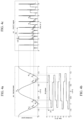
Figures 5a, 5b and 5c illustrate a modulation scheme at 8 levels when the sensor is at rest and when it is subjected to rotation at constant angular rate ω, which generates a ΔΦR phase shift by the Sagnac effect. -
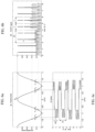
Figure 6 illustrates the effects of a gain error on the analogue modulation channel in stationary conditions when using the 8-level modulation scheme. - According to a preferred, but not limited embodiment, this invention relates a modulation technique of a MIOC of an interferometer fiber optic gyroscope, I-FOG, with closed-loop feedback control with application of a digital mod/demod approach. Said technique for modulation of the MIOC is an 8-level scheme and the duration of each level of modulation is τ\4.
- The technique for modulation of I-FOG sensors that is object of this patent application makes it possible to obtain higher dynamic performances with the same fiber length, doubling the frequency of demodulation of the signal read at the interferometer and reducing control latency from 2τ to τ. This allows, with respect to the all-digital control techniques known in the state of the art and illustrated in [1] and [2], the dynamic response of the sensors to be improved, doubling the intrinsic bandwidth and reaching higher levels of accuracy and linearity with the same quantity of fiber.
- As can be seen in
Figure 5 , illustrating the 8-level modulation scheme which drive the MIOC appropriately when the sensor is at rest and when it is subjected to rotation with constant angular rate ω, which generates a ΔΦR phase shift by the Sagnac effect, a periodical phase pattern can be identified, through the modulation channel and control logic, given by Φ0=π-α, Φ1=π+α, Φ2=-π+α, Φ3=-π-α, Φ4=-π+α, Φ5=-π-α, Φ6=π-α e Φ7=π+α (Fig. 5b ) which will correspond, at the interferometer to the values p0, p1, p2, p3, p4, p5, p6, p7. The duration of each of these values will be τ/4 (Fig. 5c ) and, once again, the duration of the entire control cycle of the I-FOG will be 2τ. However, it will be noted how the following equivalences apply:
- To modify the biasing modulation pattern so as to cancel the effect of the ΔΦR phase shift it will be necessary to add the biasing signal provided to the MIOC by a serrodyne ramp with a step having ΔVRET amplitude of duration τ and proportional to the separation of the levels p measured at the PinFET. But, while with the techniques described in [1] and [2] it was necessary to wait for a time 2τ to have a set of updated samples so as to determine the ΔVRET value, which has been said to be, in first approximation, proportional to the integral of the instant εR phase error, making it necessary to maintain the correction value unchanged for the next 2 steps of the serrodyne ramp, in the new proposed modulation scheme, as demonstrated by formulas (7) and (9), equivalences (10) and
Figure 5c , at each τ a complete and updated set of values p0, p1, p2, p3 will be available to determine:

- The value of the serrodyne ramp step (and angular rate data) can therefore be updated every τ, thus doubling the tracking speed of the feedback control of the phase shift produced by the Sagnac effect and, consequently, the bandwidth of the I-FOG sensor.
- With the εR error measurement there is the possibility of correcting the ΔΦR phase shift produced by the Sagnac effect in the I-FOG sensor with a period τ, that is, for the time necessary for propagation of the light in the sensitive element of the sensor.
- The benefits of this innovation can be imagined by thinking of a situation where the rotation rate of the sensor is not constant, but varies very quickly and, for example, between two successive time intervals τ the rotational speed ω has undergone a large variation (not a difficult thing in the presence of high entity frequency vibrations).
- By using the prior techniques, by upgrading εR only every 2τ, the phase variations produced by the Sagnac effect will be tracked with the same ΔVRET correction value for two consecutive times, producing a ΦRET phase that would no longer meet the ΦRET = -ΔΦR equality, hence committing an error that, in highly performing sensors - that can require a quantity of fiber greater than 2,000 m and consequently a propagation time τ in the coil not negligible in presence of high dynamics - can become significant and also lead to instability of the feedback control. In fact, it must be reminded that the interference pattern of the light rays after the propagation in fiber is a raised cosine and, when moving away from the selected working point, the nonlinear nature of that signal can be rapidly manifested. This phenomenon may even be exacerbated by an incorrect tracking by the feedback control.
- Thanks to an increase in the feedback dynamics of a factor of 2, the 8-level modulation technique greatly mitigates this phenomenon by reaching, for example, for a 2,000 m of fiber sensor, the same control speed and bandwidth that was, with the techniques illustrated in [1] and [2], for a sensor of 1,000 m, and to obtain, at the same fiber length, a reduction in the vibration correction effects of the sensors output, in the absence of any mechanical damping system, equal to at least one order of magnitude.
- By observing
Figure 6 , showing the effects of an analogue modulation channel gain error under stationary conditions when using the modulation technique, object of this patent application, it can be understood how also the correction speed of the gain error can be doubled, being able to evaluate εG at every τ through the formula:
- But in this case the benefits are less apparent since the MIOC half-wave voltage variations, object of the feedback effected on the modulating channel gain, are related to generally slow phenomena, such as temperature variations. With the error measurement εG it is possible to correct the MIOC modulation channel gain, in an I-FOG sensor, with periodicity equal to τ, that is, at the light propagation time in the sensing element of the sensor.
- The 8-level modulation technique allows obtaining a more accurate and linear dynamic response to the I-FOG sensors when measuring rotating rate profiles characterized by high variations (strong angular accelerations), such as it happens, for example, in the presence of vibrations. This allows mitigating the distortion effects that may occur due to the nonlinear nature of the signal measured at the interferometer, given by a raised cosine, and the latency of the feedback control.
- Through modulation technique, object of this patent application, the vibration rectification phenomenon of the I-FOG sensors can be reduced in absence of any mechanical damping system by a factor greater than one order of magnitude.
- The materials and dimensions of the invention as described above, illustrated in the accompanying drawings and as claimed below, may be any according to the requirements.
Claims (1)
- Optical phase modulating method of a MIOC (Multi Integrated Optical Circuit) of an interferometer type I-FOG fiber optic gyroscope with closed loop feedback control with digital modulation and demodulation approach comprising the step of modulating at 8 levels wherein each modulation level has a duration of one quarter of the light propagation time τ in a sensitive element consisting of a fiber optic coil.
Applications Claiming Priority (2)
| Application Number | Priority Date | Filing Date | Title |
|---|---|---|---|
| IT102017000091341A IT201700091341A1 (en) | 2017-08-07 | 2017-08-07 | Modulation scheme of the optical phase of a MIOC of an interferometric optical fiber gyroscope. |
| PCT/EP2018/025202 WO2019029845A1 (en) | 2017-08-07 | 2018-07-24 | Optical phase modulating scheme of a mioc of an interferometer type fiber optic gyroscope |
Publications (3)
| Publication Number | Publication Date |
|---|---|
| EP3665439A1 EP3665439A1 (en) | 2020-06-17 |
| EP3665439B1 true EP3665439B1 (en) | 2025-04-09 |
| EP3665439C0 EP3665439C0 (en) | 2025-04-09 |
Family
ID=60628094
Family Applications (1)
| Application Number | Title | Priority Date | Filing Date |
|---|---|---|---|
| EP18743393.3A Active EP3665439B1 (en) | 2017-08-07 | 2018-07-24 | Optical phase modulating scheme of a mioc of an interferometer type fiber optic gyroscope |
Country Status (7)
| Country | Link |
|---|---|
| US (1) | US11079231B2 (en) |
| EP (1) | EP3665439B1 (en) |
| ES (1) | ES3030183T3 (en) |
| HU (1) | HUE071269T2 (en) |
| IT (1) | IT201700091341A1 (en) |
| PL (1) | PL3665439T3 (en) |
| WO (1) | WO2019029845A1 (en) |
Families Citing this family (4)
| Publication number | Priority date | Publication date | Assignee | Title |
|---|---|---|---|---|
| FR3095053B1 (en) * | 2019-04-15 | 2021-04-16 | Ixblue | Loop or in-line fiber optic interferometer |
| CN111174773B (en) * | 2019-12-30 | 2022-04-05 | 浙江大学 | A Multi-Closed-Loop Algorithm for Fiber Optic Gyroscopes Based on Polyphase Modulation and Demodulation |
| CN113074713B (en) * | 2021-03-23 | 2023-01-24 | 安徽华驰动能科技有限公司 | High-dynamic control method of fiber-optic gyroscope |
| CN113074710A (en) * | 2021-03-23 | 2021-07-06 | 安徽华驰动能科技有限公司 | Closed-loop detection method for optimizing precision measurement precision of fiber-optic gyroscope |
Family Cites Families (6)
| Publication number | Priority date | Publication date | Assignee | Title |
|---|---|---|---|---|
| US5530545A (en) * | 1994-07-29 | 1996-06-25 | Litton Systems, Inc. | Method for reducing random walk in fiber optic gyroscopes |
| US5953123A (en) * | 1997-12-31 | 1999-09-14 | Aai Corporation | Fixed interval background auto-alignment for closed loop interferometric fiber optic gyroscopes |
| US6744519B2 (en) * | 2002-04-30 | 2004-06-01 | Honeywell International Inc. | Methods and apparatus for fiber optic gyroscope dead band error suppression modulation |
| FR2987111B1 (en) * | 2012-02-21 | 2014-03-07 | Ixblue | FIBER OPTIC MEASURING DEVICE, GYROMETER, NAVIGATION CENTER AND INERTIAL STABILIZATION |
| FR2990021B1 (en) * | 2012-04-27 | 2014-05-09 | Ixblue | FIBER OPTIC MEASURING DEVICE, GYROMETER, NAVIGATION CENTER AND INERTIAL STABILIZATION. |
| FR3011072B1 (en) * | 2013-09-24 | 2017-05-19 | Ixblue | MULTI-AXIS OPTICAL FIBER INTERFEROMETRIC SYSTEM AND METHOD FOR PROCESSING AN INTERFEROMETRIC SIGNAL IN SUCH A SYSTEM |
-
2017
- 2017-08-07 IT IT102017000091341A patent/IT201700091341A1/en unknown
-
2018
- 2018-07-24 HU HUE18743393A patent/HUE071269T2/en unknown
- 2018-07-24 WO PCT/EP2018/025202 patent/WO2019029845A1/en not_active Ceased
- 2018-07-24 ES ES18743393T patent/ES3030183T3/en active Active
- 2018-07-24 US US16/632,491 patent/US11079231B2/en active Active
- 2018-07-24 EP EP18743393.3A patent/EP3665439B1/en active Active
- 2018-07-24 PL PL18743393.3T patent/PL3665439T3/en unknown
Also Published As
| Publication number | Publication date |
|---|---|
| PL3665439T3 (en) | 2025-05-26 |
| WO2019029845A1 (en) | 2019-02-14 |
| ES3030183T3 (en) | 2025-06-26 |
| EP3665439A1 (en) | 2020-06-17 |
| IT201700091341A1 (en) | 2017-11-07 |
| EP3665439C0 (en) | 2025-04-09 |
| HUE071269T2 (en) | 2025-08-28 |
| US11079231B2 (en) | 2021-08-03 |
| US20210164782A1 (en) | 2021-06-03 |
Similar Documents
| Publication | Publication Date | Title |
|---|---|---|
| CN111174773B (en) | A Multi-Closed-Loop Algorithm for Fiber Optic Gyroscopes Based on Polyphase Modulation and Demodulation | |
| US11079231B2 (en) | Optical phase modulating scheme of a MIOC of an interferometer type fiber optic gyroscope | |
| EP3093618B1 (en) | Systems and methods for resonance switching resonator fiber optic gyroscopes (rfogs) with feed-forward processing | |
| CN115077567B (en) | Scale factor compensation system and method based on waveguide reset error | |
| EP1499856B1 (en) | Apparatus for dead band error suppression in fiber optic gyroscopes | |
| JP6404656B2 (en) | Method and apparatus for tracking / rocking the free spectral range of a resonator and its application to a resonator fiber optic gyroscope | |
| US8717575B2 (en) | Systems and methods for environmentally insensitive high-performance fiber-optic gyroscopes | |
| JP2002500376A (en) | Fiber optic gyroscope | |
| CN116184815B (en) | Closed-loop control method and system for eliminating reset error of fiber optic gyroscope | |
| US7515272B2 (en) | Digital feedback systems and methods for optical gyroscopes | |
| US10502585B2 (en) | Gyro rate computation for an interferometric fiber optic gyro | |
| CN113310483B (en) | A digital closed-loop fiber optic gyroscope eigenfrequency real-time tracking device and method | |
| RU2512599C1 (en) | Method of improving accuracy of closed-loop fibre-optic gyroscope | |
| Bergh | Dual-ramp closed-loop fiber-optic gyroscope | |
| US8301407B2 (en) | Stabilized solid-state gyrolaser | |
| Kurbatov | New methods to improve the performance of open and closed loop fiber-optic gyros | |
| CN105674976A (en) | Fiber optic gyro modulation-demodulation method, as well as method and device for improving scale factor stability | |
| CN114111754B (en) | Fiber optic gyroscope closed-loop control method and system for eliminating reset error and storage medium | |
| JP4520560B2 (en) | Method and apparatus for determining the number of fringes of an optical fiber gyro | |
| RU2512598C1 (en) | Method of reducing precision readiness time of fibre-optic gyroscope | |
| RU2194246C1 (en) | Method for processing optical fiber gyroscope ring interferometer signal | |
| JP3923077B2 (en) | How to reduce the random walk of a fiber optic gyroscope | |
| RU2627020C1 (en) | Method for improving accuracy of fiber-optic gyroscopes under vibration influence | |
| RU2523759C1 (en) | Angular velocity range extension for open-circuit fibre-optic gyro | |
| RU2626228C1 (en) | Method of improving accuracy of fibre-optic gyroscope with closed loop |
Legal Events
| Date | Code | Title | Description |
|---|---|---|---|
| STAA | Information on the status of an ep patent application or granted ep patent |
Free format text: STATUS: UNKNOWN |
|
| STAA | Information on the status of an ep patent application or granted ep patent |
Free format text: STATUS: THE INTERNATIONAL PUBLICATION HAS BEEN MADE |
|
| PUAI | Public reference made under article 153(3) epc to a published international application that has entered the european phase |
Free format text: ORIGINAL CODE: 0009012 |
|
| STAA | Information on the status of an ep patent application or granted ep patent |
Free format text: STATUS: REQUEST FOR EXAMINATION WAS MADE |
|
| 17P | Request for examination filed |
Effective date: 20200128 |
|
| AK | Designated contracting states |
Kind code of ref document: A1 Designated state(s): AL AT BE BG CH CY CZ DE DK EE ES FI FR GB GR HR HU IE IS IT LI LT LU LV MC MK MT NL NO PL PT RO RS SE SI SK SM TR |
|
| AX | Request for extension of the european patent |
Extension state: BA ME |
|
| DAV | Request for validation of the european patent (deleted) | ||
| DAX | Request for extension of the european patent (deleted) | ||
| RAP3 | Party data changed (applicant data changed or rights of an application transferred) |
Owner name: CIVITANAVI SYSTEMS S.P.A. |
|
| STAA | Information on the status of an ep patent application or granted ep patent |
Free format text: STATUS: EXAMINATION IS IN PROGRESS |
|
| 17Q | First examination report despatched |
Effective date: 20240513 |
|
| RAP3 | Party data changed (applicant data changed or rights of an application transferred) |
Owner name: CIVITANAVI SYSTEMS S.P.A. |
|
| GRAP | Despatch of communication of intention to grant a patent |
Free format text: ORIGINAL CODE: EPIDOSNIGR1 |
|
| STAA | Information on the status of an ep patent application or granted ep patent |
Free format text: STATUS: GRANT OF PATENT IS INTENDED |
|
| INTG | Intention to grant announced |
Effective date: 20250121 |
|
| GRAS | Grant fee paid |
Free format text: ORIGINAL CODE: EPIDOSNIGR3 |
|
| GRAA | (expected) grant |
Free format text: ORIGINAL CODE: 0009210 |
|
| STAA | Information on the status of an ep patent application or granted ep patent |
Free format text: STATUS: THE PATENT HAS BEEN GRANTED |
|
| AK | Designated contracting states |
Kind code of ref document: B1 Designated state(s): AL AT BE BG CH CY CZ DE DK EE ES FI FR GB GR HR HU IE IS IT LI LT LU LV MC MK MT NL NO PL PT RO RS SE SI SK SM TR |
|
| REG | Reference to a national code |
Ref country code: GB Ref legal event code: FG4D |
|
| REG | Reference to a national code |
Ref country code: CH Ref legal event code: EP |
|
| REG | Reference to a national code |
Ref country code: DE Ref legal event code: R096 Ref document number: 602018080947 Country of ref document: DE |
|
| REG | Reference to a national code |
Ref country code: IE Ref legal event code: FG4D |
|
| U01 | Request for unitary effect filed |
Effective date: 20250507 |
|
| U07 | Unitary effect registered |
Designated state(s): AT BE BG DE DK EE FI FR IT LT LU LV MT NL PT RO SE SI Effective date: 20250513 |
|
| REG | Reference to a national code |
Ref country code: ES Ref legal event code: FG2A Ref document number: 3030183 Country of ref document: ES Kind code of ref document: T3 Effective date: 20250626 |
|
| PGFP | Annual fee paid to national office [announced via postgrant information from national office to epo] |
Ref country code: PL Payment date: 20250627 Year of fee payment: 8 |
|
| PGFP | Annual fee paid to national office [announced via postgrant information from national office to epo] |
Ref country code: CZ Payment date: 20250625 Year of fee payment: 8 |
|
| PGFP | Annual fee paid to national office [announced via postgrant information from national office to epo] |
Ref country code: HU Payment date: 20250627 Year of fee payment: 8 |
|
| REG | Reference to a national code |
Ref country code: GR Ref legal event code: EP Ref document number: 20250400885 Country of ref document: GR Effective date: 20250613 |
|
| U20 | Renewal fee for the european patent with unitary effect paid |
Year of fee payment: 8 Effective date: 20250722 |
|
| REG | Reference to a national code |
Ref country code: HU Ref legal event code: AG4A Ref document number: E071269 Country of ref document: HU |
|
| PGFP | Annual fee paid to national office [announced via postgrant information from national office to epo] |
Ref country code: ES Payment date: 20250801 Year of fee payment: 8 |
|
| PGFP | Annual fee paid to national office [announced via postgrant information from national office to epo] |
Ref country code: NO Payment date: 20250729 Year of fee payment: 8 Ref country code: GR Payment date: 20250721 Year of fee payment: 8 |
|
| PGFP | Annual fee paid to national office [announced via postgrant information from national office to epo] |
Ref country code: TR Payment date: 20250722 Year of fee payment: 8 |
|
| PGFP | Annual fee paid to national office [announced via postgrant information from national office to epo] |
Ref country code: GB Payment date: 20250725 Year of fee payment: 8 |
|
| PG25 | Lapsed in a contracting state [announced via postgrant information from national office to epo] |
Ref country code: HR Free format text: LAPSE BECAUSE OF FAILURE TO SUBMIT A TRANSLATION OF THE DESCRIPTION OR TO PAY THE FEE WITHIN THE PRESCRIBED TIME-LIMIT Effective date: 20250409 |
|
| PGFP | Annual fee paid to national office [announced via postgrant information from national office to epo] |
Ref country code: CH Payment date: 20250801 Year of fee payment: 8 |
|
| PG25 | Lapsed in a contracting state [announced via postgrant information from national office to epo] |
Ref country code: RS Free format text: LAPSE BECAUSE OF FAILURE TO SUBMIT A TRANSLATION OF THE DESCRIPTION OR TO PAY THE FEE WITHIN THE PRESCRIBED TIME-LIMIT Effective date: 20250709 |
|
| PGFP | Annual fee paid to national office [announced via postgrant information from national office to epo] |
Ref country code: IE Payment date: 20250723 Year of fee payment: 8 |
|
| PG25 | Lapsed in a contracting state [announced via postgrant information from national office to epo] |
Ref country code: IS Free format text: LAPSE BECAUSE OF FAILURE TO SUBMIT A TRANSLATION OF THE DESCRIPTION OR TO PAY THE FEE WITHIN THE PRESCRIBED TIME-LIMIT Effective date: 20250809 |
|
| PG25 | Lapsed in a contracting state [announced via postgrant information from national office to epo] |
Ref country code: SM Free format text: LAPSE BECAUSE OF FAILURE TO SUBMIT A TRANSLATION OF THE DESCRIPTION OR TO PAY THE FEE WITHIN THE PRESCRIBED TIME-LIMIT Effective date: 20250409 |
|
| PG25 | Lapsed in a contracting state [announced via postgrant information from national office to epo] |
Ref country code: SK Free format text: LAPSE BECAUSE OF FAILURE TO SUBMIT A TRANSLATION OF THE DESCRIPTION OR TO PAY THE FEE WITHIN THE PRESCRIBED TIME-LIMIT Effective date: 20250409 |
|
| PLBE | No opposition filed within time limit |
Free format text: ORIGINAL CODE: 0009261 |
|
| STAA | Information on the status of an ep patent application or granted ep patent |
Free format text: STATUS: NO OPPOSITION FILED WITHIN TIME LIMIT |
|
| REG | Reference to a national code |
Ref country code: CH Ref legal event code: L10 Free format text: ST27 STATUS EVENT CODE: U-0-0-L10-L00 (AS PROVIDED BY THE NATIONAL OFFICE) Effective date: 20260218 |
|
| 26N | No opposition filed |
Effective date: 20260112 |