EP3663892A1 - Memory module with screen and motherboard module - Google Patents
Memory module with screen and motherboard module Download PDFInfo
- Publication number
- EP3663892A1 EP3663892A1 EP19204446.9A EP19204446A EP3663892A1 EP 3663892 A1 EP3663892 A1 EP 3663892A1 EP 19204446 A EP19204446 A EP 19204446A EP 3663892 A1 EP3663892 A1 EP 3663892A1
- Authority
- EP
- European Patent Office
- Prior art keywords
- memory
- screen
- module
- power conversion
- disposed
- Prior art date
- Legal status (The legal status is an assumption and is not a legal conclusion. Google has not performed a legal analysis and makes no representation as to the accuracy of the status listed.)
- Granted
Links
Images



Classifications
-
- G—PHYSICS
- G11—INFORMATION STORAGE
- G11C—STATIC STORES
- G11C5/00—Details of stores covered by group G11C11/00
- G11C5/02—Disposition of storage elements, e.g. in the form of a matrix array
- G11C5/04—Supports for storage elements, e.g. memory modules; Mounting or fixing of storage elements on such supports
-
- G—PHYSICS
- G06—COMPUTING OR CALCULATING; COUNTING
- G06F—ELECTRIC DIGITAL DATA PROCESSING
- G06F1/00—Details not covered by groups G06F3/00 - G06F13/00 and G06F21/00
- G06F1/16—Constructional details or arrangements
- G06F1/18—Packaging or power distribution
- G06F1/183—Internal mounting support structures, e.g. for supporting printed circuit boards
-
- G—PHYSICS
- G06—COMPUTING OR CALCULATING; COUNTING
- G06F—ELECTRIC DIGITAL DATA PROCESSING
- G06F1/00—Details not covered by groups G06F3/00 - G06F13/00 and G06F21/00
- G06F1/16—Constructional details or arrangements
- G06F1/1601—Constructional details related to the housing of computer displays, e.g. of CRT monitors, of flat displays
-
- G—PHYSICS
- G06—COMPUTING OR CALCULATING; COUNTING
- G06F—ELECTRIC DIGITAL DATA PROCESSING
- G06F1/00—Details not covered by groups G06F3/00 - G06F13/00 and G06F21/00
- G06F1/16—Constructional details or arrangements
- G06F1/18—Packaging or power distribution
- G06F1/183—Internal mounting support structures, e.g. for supporting printed circuit boards
- G06F1/185—Mounting of expansion boards
-
- G—PHYSICS
- G06—COMPUTING OR CALCULATING; COUNTING
- G06F—ELECTRIC DIGITAL DATA PROCESSING
- G06F1/00—Details not covered by groups G06F3/00 - G06F13/00 and G06F21/00
- G06F1/16—Constructional details or arrangements
- G06F1/18—Packaging or power distribution
- G06F1/183—Internal mounting support structures, e.g. for supporting printed circuit boards
- G06F1/185—Mounting of expansion boards
- G06F1/186—Securing of expansion boards in correspondence to slots provided at the computer enclosure
-
- G—PHYSICS
- G06—COMPUTING OR CALCULATING; COUNTING
- G06F—ELECTRIC DIGITAL DATA PROCESSING
- G06F1/00—Details not covered by groups G06F3/00 - G06F13/00 and G06F21/00
- G06F1/16—Constructional details or arrangements
- G06F1/20—Cooling means
-
- G—PHYSICS
- G06—COMPUTING OR CALCULATING; COUNTING
- G06F—ELECTRIC DIGITAL DATA PROCESSING
- G06F1/00—Details not covered by groups G06F3/00 - G06F13/00 and G06F21/00
- G06F1/26—Power supply means, e.g. regulation thereof
- G06F1/32—Means for saving power
- G06F1/3203—Power management, i.e. event-based initiation of a power-saving mode
- G06F1/3206—Monitoring of events, devices or parameters that trigger a change in power modality
- G06F1/3215—Monitoring of peripheral devices
- G06F1/3225—Monitoring of peripheral devices of memory devices
-
- H—ELECTRICITY
- H05—ELECTRIC TECHNIQUES NOT OTHERWISE PROVIDED FOR
- H05K—PRINTED CIRCUITS; CASINGS OR CONSTRUCTIONAL DETAILS OF ELECTRIC APPARATUS; MANUFACTURE OF ASSEMBLAGES OF ELECTRICAL COMPONENTS
- H05K1/00—Printed circuits
- H05K1/02—Details
- H05K1/0201—Thermal arrangements, e.g. for cooling, heating or preventing overheating
- H05K1/0203—Cooling of mounted components
-
- H—ELECTRICITY
- H05—ELECTRIC TECHNIQUES NOT OTHERWISE PROVIDED FOR
- H05K—PRINTED CIRCUITS; CASINGS OR CONSTRUCTIONAL DETAILS OF ELECTRIC APPARATUS; MANUFACTURE OF ASSEMBLAGES OF ELECTRICAL COMPONENTS
- H05K1/00—Printed circuits
- H05K1/18—Printed circuits structurally associated with non-printed electric components
- H05K1/182—Printed circuits structurally associated with non-printed electric components associated with components mounted in printed circuit boards [PCB], e.g. insert-mounted components [IMC]
-
- H—ELECTRICITY
- H05—ELECTRIC TECHNIQUES NOT OTHERWISE PROVIDED FOR
- H05K—PRINTED CIRCUITS; CASINGS OR CONSTRUCTIONAL DETAILS OF ELECTRIC APPARATUS; MANUFACTURE OF ASSEMBLAGES OF ELECTRICAL COMPONENTS
- H05K7/00—Constructional details common to different types of electric apparatus
- H05K7/14—Mounting supporting structure in casing or on frame or rack
- H05K7/1417—Mounting supporting structure in casing or on frame or rack having securing means for mounting boards, plates or wiring boards
- H05K7/1418—Card guides, e.g. grooves
-
- H—ELECTRICITY
- H01—ELECTRIC ELEMENTS
- H01R—ELECTRICALLY-CONDUCTIVE CONNECTIONS; STRUCTURAL ASSOCIATIONS OF A PLURALITY OF MUTUALLY-INSULATED ELECTRICAL CONNECTING ELEMENTS; COUPLING DEVICES; CURRENT COLLECTORS
- H01R12/00—Structural associations of a plurality of mutually-insulated electrical connecting elements, specially adapted for printed circuits, e.g. printed circuit boards [PCB], flat or ribbon cables, or like generally planar structures, e.g. terminal strips, terminal blocks; Coupling devices specially adapted for printed circuits, flat or ribbon cables, or like generally planar structures; Terminals specially adapted for contact with, or insertion into, printed circuits, flat or ribbon cables, or like generally planar structures
- H01R12/70—Coupling devices
- H01R12/71—Coupling devices for rigid printing circuits or like structures
- H01R12/72—Coupling devices for rigid printing circuits or like structures coupling with the edge of the rigid printed circuits or like structures
- H01R12/73—Coupling devices for rigid printing circuits or like structures coupling with the edge of the rigid printed circuits or like structures connecting to other rigid printed circuits or like structures
- H01R12/735—Printed circuits including an angle between each other
- H01R12/737—Printed circuits being substantially perpendicular to each other
-
- H—ELECTRICITY
- H05—ELECTRIC TECHNIQUES NOT OTHERWISE PROVIDED FOR
- H05K—PRINTED CIRCUITS; CASINGS OR CONSTRUCTIONAL DETAILS OF ELECTRIC APPARATUS; MANUFACTURE OF ASSEMBLAGES OF ELECTRICAL COMPONENTS
- H05K1/00—Printed circuits
- H05K1/02—Details
- H05K1/14—Structural association of two or more printed circuits
- H05K1/141—One or more single auxiliary printed circuits mounted on a main printed circuit, e.g. modules, adapters
-
- H—ELECTRICITY
- H05—ELECTRIC TECHNIQUES NOT OTHERWISE PROVIDED FOR
- H05K—PRINTED CIRCUITS; CASINGS OR CONSTRUCTIONAL DETAILS OF ELECTRIC APPARATUS; MANUFACTURE OF ASSEMBLAGES OF ELECTRICAL COMPONENTS
- H05K2201/00—Indexing scheme relating to printed circuits covered by H05K1/00
- H05K2201/10—Details of components or other objects attached to or integrated in a printed circuit board
- H05K2201/10007—Types of components
- H05K2201/10106—Light emitting diode [LED]
-
- H—ELECTRICITY
- H05—ELECTRIC TECHNIQUES NOT OTHERWISE PROVIDED FOR
- H05K—PRINTED CIRCUITS; CASINGS OR CONSTRUCTIONAL DETAILS OF ELECTRIC APPARATUS; MANUFACTURE OF ASSEMBLAGES OF ELECTRICAL COMPONENTS
- H05K2201/00—Indexing scheme relating to printed circuits covered by H05K1/00
- H05K2201/10—Details of components or other objects attached to or integrated in a printed circuit board
- H05K2201/10007—Types of components
- H05K2201/10128—Display
-
- H—ELECTRICITY
- H05—ELECTRIC TECHNIQUES NOT OTHERWISE PROVIDED FOR
- H05K—PRINTED CIRCUITS; CASINGS OR CONSTRUCTIONAL DETAILS OF ELECTRIC APPARATUS; MANUFACTURE OF ASSEMBLAGES OF ELECTRICAL COMPONENTS
- H05K2201/00—Indexing scheme relating to printed circuits covered by H05K1/00
- H05K2201/10—Details of components or other objects attached to or integrated in a printed circuit board
- H05K2201/10007—Types of components
- H05K2201/10128—Display
- H05K2201/10136—Liquid Crystal display [LCD]
-
- H—ELECTRICITY
- H05—ELECTRIC TECHNIQUES NOT OTHERWISE PROVIDED FOR
- H05K—PRINTED CIRCUITS; CASINGS OR CONSTRUCTIONAL DETAILS OF ELECTRIC APPARATUS; MANUFACTURE OF ASSEMBLAGES OF ELECTRICAL COMPONENTS
- H05K2201/00—Indexing scheme relating to printed circuits covered by H05K1/00
- H05K2201/10—Details of components or other objects attached to or integrated in a printed circuit board
- H05K2201/10007—Types of components
- H05K2201/10159—Memory
-
- H—ELECTRICITY
- H05—ELECTRIC TECHNIQUES NOT OTHERWISE PROVIDED FOR
- H05K—PRINTED CIRCUITS; CASINGS OR CONSTRUCTIONAL DETAILS OF ELECTRIC APPARATUS; MANUFACTURE OF ASSEMBLAGES OF ELECTRICAL COMPONENTS
- H05K2201/00—Indexing scheme relating to printed circuits covered by H05K1/00
- H05K2201/10—Details of components or other objects attached to or integrated in a printed circuit board
- H05K2201/10227—Other objects, e.g. metallic pieces
- H05K2201/10356—Cables
Definitions
- the invention relates to a memory module and a motherboard module, and in particular, to a memory module with a screen and a motherboard module.
- the light-emitting components may not provide more functions for the user.
- the invention provides a memory module with a screen, which does not occupy a power supply slot on the motherboard, and may display text messages and images.
- the invention provides a motherboard module including the memory module with the screen.
- a memory module with a screen of the invention includes a memory substrate, a power conversion module, a screen control module, and a screen.
- the memory substrate includes a plurality of memory components and a connection interface.
- the power conversion module is disposed on the memory substrate and electrically connected to the connection interface.
- the screen control module is disposed on the memory substrate and electrically connected to the connection interface and the power conversion module.
- the screen is disposed on the memory substrate, and the screen is electrically connected to the power conversion module and the screen control module to receive a voltage output from the power conversion module and a display signal output from the screen control module.
- the power conversion module and the screen control module are electrically connected to a plurality of empty pins of the connection interface of the memory substrate.
- the memory substrate further includes a standard height region and an expansion region, the expansion region is disposed beside the standard height region and away from the connection interface, the plurality of memory components are disposed in the standard height region, and the power conversion module and the screen control module are disposed on the expansion region.
- a heat dissipation cover is further disposed on the memory substrate and thermally coupled to the plurality of memory components.
- the heat dissipation cover has a surface, the screen is disposed on the surface, and the screen is thermally coupled to the surface.
- a flexible cable is further respectively connected to the screen and the memory substrate, and the screen is electrically connected to the power conversion module and the screen control module via the flexible cable.
- the motherboard module of the invention includes a motherboard, a memory module with a screen, a power conversion module, and a screen control module.
- the motherboard includes a memory slot.
- the memory module with the screen is detachably inserted into the memory slots.
- the memory module with the screen includes a memory substrate and a screen.
- the memory substrate includes a plurality of memory components and a connection interface, and the connection interface is detachably inserted into the corresponding memory slot.
- the screen is disposed on the memory substrate.
- the power conversion module is disposed on the memory substrate and electrically connected to the connection interface, or disposed on the motherboard and electrically connected to the memory slot.
- the screen control module is disposed on the memory substrate and electrically connected to the connection interface and the power conversion module, or is disposed on the motherboard and electrically connected to the memory slot and the power conversion module.
- the screen is electrically connected to the power conversion module and the screen control module to receive a voltage output by the power conversion module and a display signal output by the screen control module.
- the power conversion module and the screen control module are electrically connected to a plurality of empty pins of the connection interface of the memory substrate.
- the memory substrate is provided with the power conversion module and the screen control module, and the memory substrate further includes a standard height region and an expansion region, and the expansion region is disposed beside the standard height region and away from the connection interface, and in each memory substrate, the plurality of memory components are disposed in the standard height region, and the power conversion module and the screen control module are disposed on the expansion region.
- the memory module with the screen further includes a heat dissipation cover disposed on the memory substrate and thermally coupled to the plurality of memory components, the heat dissipation cover includes a surface, and the screen is disposed on the surface and thermally coupled to the heat dissipation cover.
- the memory module with the screen further includes a flexible cable fixed to the memory substrate, and the screen is electrically connected to the power conversion module and the screen control module via the flexible cable.
- the memory module with the screen includes the memory modules with the screen, and when the memory modules with the screen are inserted into the memory slots, the screens of the memory modules with the screen are spliced together into a combined screen.
- the screen of the memory module with the screen of the invention is electrically connected to the power conversion module and the screen control module, and the power conversion module and the screen control module are electrically connected to the connection interface.
- the power conversion module and the screen control module receive a signal from the motherboard via the memory slots.
- the power conversion module converts the voltage from the memory slots into the voltage required by the screen, and the screen control module processes the signal from the memory slots to control the screen displayed by the screen. Therefore, since the screen of the memory module with the screen of the invention shares the memory slots on the motherboard with the memory substrate, the motherboard does not need to have an additional slot for power supply and signal, thereby saving space on the motherboard.
- the screen of the memory module with the screen of the invention may display text messages and images to provide users with more information and visual effects.
- the power conversion module and the screen control module may also be optionally disposed on the motherboard and electrically connected to the memory slot, so that the screen of the memory module with the screen may still obtain the required voltage and control signal via the memory slots.
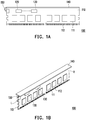
- FIG. 1A is a schematic view of a memory module with a screen in accordance with an embodiment of the invention.
- FIG. 1B is a perspective view of the memory module with the screen of FIG. 1A .
- a memory module 100 with a screen includes a memory substrate 110, a power conversion module 120, a screen control module 130, and a screen 140.
- the memory substrate 110 includes a plurality of memory components 111 and a connection interface 112.
- the connection interface 112 is, for example, a connection interface of a gold finger structure, but is not limited thereto.
- the power conversion module 120 is disposed on the memory substrate 110 and electrically connected (shown in broken lines) to the connection interface 112.
- the screen control module 130 is disposed on the memory substrate 110 and electrically connected to the connection interface 112 and the power conversion module 120.
- the screen 140 is disposed on the memory substrate 110, and the screen 140 is electrically connected to the power conversion module 120 and the screen control module 130 to receive a voltage output from the power conversion module 120 and a display signal output from the screen control module 130.
- the power conversion module 120 and the screen control module 130 are disposed on a lateral surface R of the memory substrate 110 the same as the memory components 111, but is not limited thereto. As long as the components on the memory substrate 110 do not interfere with each other, the power conversion module 120 and the screen control module 130 may also be disposed on another lateral surface L of the memory substrate 110, or the power conversion module 120 and the screen control module 130 may be disposed separately on the two lateral surfaces R and L on the memory substrate 110.
- the power conversion module 120 includes an integrated circuit, a passive component, a boosting circuit, a step-down circuit, or a combination thereof (not shown).
- the power conversion module 120 converts the initial voltage from the connection interface 112 into a converted voltage.
- the converted voltage is provided to the screen 140 and the screen control module 130, wherein the initial voltage is, for example, a voltage such as 0.6 volts, 1.2 volts, or 2.5 volts, and the converted voltage is, for example, 3.3 volts or the total voltage of the screen 140 plus other integrated circuits.
- the reason why the memory module 100 with the screen is provided with the power conversion module 120 is that the initial voltage from the connection interface 112 may only be used by the memory substrate 110 and cannot be directly provided to the screen 140 for use.
- an external screen is to be powered, an additional slot needs to be provided to provide a suitable voltage to the external screen, and the motherboard used in the memory module 100 with the screen of the present embodiment does not need to be additionally provided with an electrical slot exclusive for the screen 140.
- the memory module 100 with the screen of the present embodiment may directly convert the initial voltage into an appropriate voltage via the power conversion module 120 for use by the screen 140 and the screen control module 130 to save space on the motherboard.
- the screen control module 130 includes an integrated circuit, a passive component, a boosting circuit, a step-down circuit, or a combination thereof (not shown).
- the screen control module 130 receives the voltage provided by the power conversion module 120 and is electrically connected to the serial data (SDA) and the serial clock (SCL) of the connection interface 112 to obtain a signal from the motherboard.
- the motherboard may operate the display signal provided to the screen 140 by the screen control module 130 via a software or an application, for example, via a software or an application to switch display information, display graphics, etc., to provide users with more functionality and entertainment.
- the pins on the connection interface 112 of the gold finger structure of the memory substrate 110 leave empty pins (that is, undefined pin positions).
- the power conversion module 120 and the screen control module 130 are electrically connected to the memory slots on the motherboard via the empty pins of the connection interface 112 of the gold finger structure.
- the empty pins are, for example, the pin position number 47, 49, 54, 56, 93, 192, 194, 196, 197, 199, 201, 230, 234, 235, or 237 located on the connection interface 112 of the gold finger structure.
- the memory substrate 110 of the memory module 100 with the screen may still transmit the memory signal along the original pin position, and the signal transmission of the power conversion module 120 and the screen control module 130 does not affect the transmission of the original memory signal.
- the memory module 100 with the screen adopts a memory substrate 110 of a general industrial grade, and the height thereof is, for example, between 1.1 inches and 1.2 inches, and the memory components 111 are disposed on the memory substrate 110 that is closer to the connection interface 112 than the power conversion module 120 and the screen control module 130. That is, the plurality of memory components 111 are moved down to a position close to the connection interface 112, and the power conversion module 120 and the screen control module 130 are disposed above the plurality of memory components 111 and near the screen 140.
- the configuration of the memory components 111, the power conversion module 120, and the screen control module 130 is not limited thereto, and as long as the components on the memory substrate 110 do not interfere with each other, the configuration of the memory components 111, the power conversion module 120, and the screen control module 130 may be adjusted as required by the process.
- the memory module 100 with the screen further includes a flexible cable 150, and the flexible cable 150 is fixed to the memory substrate 110, and the manner of fixing is, for example, snapping, inlaying, or bonding, and is not limited thereto.
- the flexible cable 150 is electrically connected to the screen 140 and the memory substrate 110 via the wires inside that are not exposed, and the screen 140 may be electrically connected to the power conversion module 120 and the screen control module 130 via the flexible cable 150.
- the screen 140 may also be directly electrically connected to the power conversion module 120 and the screen control module 130 without the flexible cable 150.
- the method of electrical connection of the screen 140 to the power conversion module 120 and the screen control module 130 is not limited thereto.
- FIG. 2 is a schematic view of the memory module with the screen of FIG. 1A inserted into a motherboard.
- the motherboard module 10 includes the motherboard 11 and the memory module 100 with the screen.
- the motherboard 11 includes memory slots 11a.
- the connection interface 112 of the memory module 100 with the screen is detachably inserted into the memory slot 11a.
- only four memory slots 11a are schematically illustrated in FIG. 2 . In actuality, the number of the memory slots 11a may also be two or eight, and is not limited thereto.
- the power conversion module 120 and the screen control module 130 receive a signal from the motherboard 11 via the memory slot 11a.
- the power conversion module 120 converts the voltage from the memory slot 11a into the voltage required by the screen 140, and the screen control module 130 processes the signal from the memory slot 11a to control the picture displayed by the screen 140. Therefore, the screen 140 may display text messages or images, such as text messages or images such as the operating frequency or operating temperature of a central processing unit (CPU) to provide users with more functionality.
- CPU central processing unit
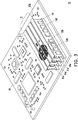
- FIG. 3 is a schematic view of a plurality of the memory module with the screen of FIG. 1A inserted into a motherboard.
- the four screens 140 of the four memory modules 100 with the screen are combined into a combined screen S, and the combined screen S may display a large area of text messages or images.
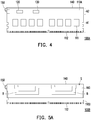
- FIG. 4 is a front view of a memory module with a screen in accordance with another embodiment of the invention.
- FIG. 4 is slightly different from the memory module with the screen of FIG. 1A to FIG. 1B .
- the difference is the height of the memory substrate.
- a memory substrate 110A is the memory substrate 110 heightened.
- Such a memory module 100A with the screen has a greater area, so that the components on the memory substrate 110A may be disposed on the memory substrate 110A with less space limit.
- the memory substrate 110A further includes a standard height region A1 and an expansion region A2.
- the expansion region A2 is disposed beside the standard height region A1 and away from the connection interface 112.
- the sum of the heights of the standard height region A1 and the extension region A2 is greater than 1.2 inches.
- the memory components 111 are disposed in the standard height region A1, and the power conversion module 120 and the screen control module 130 are disposed on the expansion region A2.
- the configuration of the memory components 111, the power conversion module 120, and the screen control module 130 is not limited thereto, and any configuration in which the components on the memory substrate 110A do not interfere with each other is within the scope of the invention.
- FIG. 5A is a front view of a memory module with a screen in accordance with another embodiment of the invention.
- FIG. 5B is a perspective view of the memory module with the screen of FIG. 5A .
- a memory module 100B with a screen further includes a heat dissipation cover 160 compared to the memory modules 100 and 100A with the screen.
- the heat dissipation cover 160 is clamped on the memory substrate 110B via a clip B, but is not limited thereto.
- the memory module 100B with the screen may not need the clip B, and instead the heat dissipation cover 160 may be fixed on the memory substrate 110B using a bonding method.
- the heat dissipation cover 160 is disposed on the memory substrate 110B and thermally coupled to the memory components 111. It should be noted that the memory components 111 are covered by the heat dissipation cover 160, so that the memory components cannot be seen in FIG. 5A and FIG. 5B .
- the heat dissipation cover 160 has a surface S, the screen 140 is disposed on the surface S, and the screen 140 is thermally coupled to the surface S. That is to say, the heat dissipation cover 160 has a function of simultaneously helping the memory components 111 and the screen 140 to dissipate heat.
- the surface S is, for example, the top surface of the heat dissipation cover 160, but is not limited thereto. In other embodiments, the surface S may also be the side surface of the heat dissipation cover 160.
- FIG. 6 is a perspective view of a memory module with a screen according to another embodiment of the invention.
- the surface S is a side surface of the heat dissipation cover 160
- the screen 140 is disposed on the surface S of the heat dissipation cover 160.
- the memory modules with the screen in FIGs. 5A and 5B or FIG. 6 may also include the flexible cable 150.
- the flexible cable 150 may also be fixed on the heat dissipation cover 160.
- the fixing method is, for example, engaging, inlaying, or bonding, but is not limited thereto, and any method in which the flexible cable 150 may be fixed to the memory substrate is within the scope of the invention.
- FIG. 7 is a front view of a memory module with a screen in accordance with another embodiment of the invention.
- FIG. 8 is a schematic diagram of a motherboard module in accordance with another embodiment of the invention. Referring to FIG. 7 and FIG. 8 , the main difference between a motherboard module 10C and the motherboard module 10 is that a power conversion module 120C and a screen control module 130C are both disposed on a motherboard 11C.
- the memory module 100C with the screen may be inserted into one of the memory slots 11a.
- the power conversion module 120C is disposed on the motherboard 11C and electrically connected to the memory slots 11a.
- the screen control module 130C is disposed on the motherboard 11C and electrically connected to the memory slots 11a and the power conversion module 120C.
- the power conversion module 120C converts the initial voltage from the circuit of the motherboard 11C into the converted voltage required by the screen 140, and the converted voltage passes through one of the empty pins on the connection interface 112 to supply power to the screen 140. That is to say, in the present embodiment, the voltage passing through the empty pin is the voltage required by the screen 140.
- the advantage of the present embodiment is that the memory manufacturer does not need to significantly change the design of the memory substrate 110C, and the screen 140 only needs to be disposed on the memory substrate 110C.
- FIG. 8 only schematically shows four memory slots 11a, four power conversion modules 120C and four screen control modules 130C, and in actuality, the number of the memory slots 11a may also be two or eight and is not limited thereto.
- the number of the power conversion module 120C and the screen control modules 130C is configured according to the corresponding number of the memory module 100C with the screen.
- the four screens 140 of the four memory modules 100 with the screen are combined into the combined screen S of FIG. 3 , and the combined screen S may display text messages or images.
- the screen of the memory module with the screen of the invention is electrically connected to the power conversion module and the screen control module, and the power conversion module and the screen control module are electrically connected to the connection interface.
- the power conversion module and the screen control module receive a signal from the motherboard via the memory slot.
- the power conversion module converts the voltage from the memory slot into the voltage required by the screen, and the screen control module processes the signal from the memory slot to control the image displayed by the screen. Therefore, since the screen of the memory module with the screen of the invention shares the memory slots on the motherboard with the memory substrate, the motherboard does not need to have an additional slot for power supply and signal, thereby saving space on the motherboard.
- the screen of the memory module with the screen of the invention may display text messages and images to provide users with more information and visual effects.
- the power conversion module and the screen control module may also be selectively disposed on the motherboard and electrically connected to the memory slots, so that the screen of the memory module with the screen may still obtain the required voltage and control signal via the memory slots.
- the user may operate the screen control module via a software or an application to provide users with a more diverse functionality. In this way, the memory module with the screen may provide more information and entertainment to the user without increasing the burden of motherboard space configuration.
Landscapes
- Engineering & Computer Science (AREA)
- Theoretical Computer Science (AREA)
- General Engineering & Computer Science (AREA)
- Physics & Mathematics (AREA)
- General Physics & Mathematics (AREA)
- Human Computer Interaction (AREA)
- Computer Hardware Design (AREA)
- Power Engineering (AREA)
- Microelectronics & Electronic Packaging (AREA)
- Devices For Indicating Variable Information By Combining Individual Elements (AREA)
- Memory System (AREA)
- Semiconductor Memories (AREA)
- Multimedia (AREA)
- Control Of Indicators Other Than Cathode Ray Tubes (AREA)
- User Interface Of Digital Computer (AREA)
- Debugging And Monitoring (AREA)
Abstract
Description
- The invention relates to a memory module and a motherboard module, and in particular, to a memory module with a screen and a motherboard module.
- In recent years, with the rapid development and advancement of technology, desktop computers have become quite common. At present, in order to provide users with more visual effects, some motherboards are provided with light-emitting components (such as LEDs), and additional slots are provided to insert the light-emitting components into the slots, so that the light-emitting components directly receive the voltage output from the motherboard.
- However, in addition to achieving the effect of light conversion, the light-emitting components may not provide more functions for the user.
- The invention provides a memory module with a screen, which does not occupy a power supply slot on the motherboard, and may display text messages and images.
- The invention provides a motherboard module including the memory module with the screen.
- A memory module with a screen of the invention includes a memory substrate, a power conversion module, a screen control module, and a screen. The memory substrate includes a plurality of memory components and a connection interface. The power conversion module is disposed on the memory substrate and electrically connected to the connection interface. The screen control module is disposed on the memory substrate and electrically connected to the connection interface and the power conversion module. The screen is disposed on the memory substrate, and the screen is electrically connected to the power conversion module and the screen control module to receive a voltage output from the power conversion module and a display signal output from the screen control module.
- In an embodiment of the invention, the power conversion module and the screen control module are electrically connected to a plurality of empty pins of the connection interface of the memory substrate.
- In an embodiment of the invention, the memory substrate further includes a standard height region and an expansion region, the expansion region is disposed beside the standard height region and away from the connection interface, the plurality of memory components are disposed in the standard height region, and the power conversion module and the screen control module are disposed on the expansion region.
- In an embodiment of the invention, a heat dissipation cover is further disposed on the memory substrate and thermally coupled to the plurality of memory components. The heat dissipation cover has a surface, the screen is disposed on the surface, and the screen is thermally coupled to the surface.
- In an embodiment of the invention, a flexible cable is further respectively connected to the screen and the memory substrate, and the screen is electrically connected to the power conversion module and the screen control module via the flexible cable.
- The motherboard module of the invention includes a motherboard, a memory module with a screen, a power conversion module, and a screen control module. The motherboard includes a memory slot. The memory module with the screen is detachably inserted into the memory slots. The memory module with the screen includes a memory substrate and a screen. The memory substrate includes a plurality of memory components and a connection interface, and the connection interface is detachably inserted into the corresponding memory slot. The screen is disposed on the memory substrate. The power conversion module is disposed on the memory substrate and electrically connected to the connection interface, or disposed on the motherboard and electrically connected to the memory slot. The screen control module is disposed on the memory substrate and electrically connected to the connection interface and the power conversion module, or is disposed on the motherboard and electrically connected to the memory slot and the power conversion module. In particular, when the memory module with the screen is inserted into the memory slot, the screen is electrically connected to the power conversion module and the screen control module to receive a voltage output by the power conversion module and a display signal output by the screen control module.
- In an embodiment of the invention, the power conversion module and the screen control module are electrically connected to a plurality of empty pins of the connection interface of the memory substrate.
- In an embodiment of the invention, the memory substrate is provided with the power conversion module and the screen control module, and the memory substrate further includes a standard height region and an expansion region, and the expansion region is disposed beside the standard height region and away from the connection interface, and in each memory substrate, the plurality of memory components are disposed in the standard height region, and the power conversion module and the screen control module are disposed on the expansion region.
- In an embodiment of the invention, the memory module with the screen further includes a heat dissipation cover disposed on the memory substrate and thermally coupled to the plurality of memory components, the heat dissipation cover includes a surface, and the screen is disposed on the surface and thermally coupled to the heat dissipation cover.
- In an embodiment of the invention, the memory module with the screen further includes a flexible cable fixed to the memory substrate, and the screen is electrically connected to the power conversion module and the screen control module via the flexible cable.
- In an embodiment of the invention, the memory module with the screen includes the memory modules with the screen, and when the memory modules with the screen are inserted into the memory slots, the screens of the memory modules with the screen are spliced together into a combined screen.
- Based on the above, the screen of the memory module with the screen of the invention is electrically connected to the power conversion module and the screen control module, and the power conversion module and the screen control module are electrically connected to the connection interface. When the memory module with the screen is inserted into the memory slot, the power conversion module and the screen control module receive a signal from the motherboard via the memory slots. The power conversion module converts the voltage from the memory slots into the voltage required by the screen, and the screen control module processes the signal from the memory slots to control the screen displayed by the screen. Therefore, since the screen of the memory module with the screen of the invention shares the memory slots on the motherboard with the memory substrate, the motherboard does not need to have an additional slot for power supply and signal, thereby saving space on the motherboard. In addition, the screen of the memory module with the screen of the invention may display text messages and images to provide users with more information and visual effects. In addition, in an embodiment, the power conversion module and the screen control module may also be optionally disposed on the motherboard and electrically connected to the memory slot, so that the screen of the memory module with the screen may still obtain the required voltage and control signal via the memory slots.
- In order to make the aforementioned features and advantages of the disclosure more comprehensible, embodiments accompanied with figures are described in detail below.
- The accompanying drawings are included to provide a further understanding of the invention, and are incorporated in and constitute a part of this specification. The drawings illustrate embodiments of the invention and, together with the description, serve to explain the principles of the invention.
-
FIG. 1A is a front view of a memory module with a screen in accordance with an embodiment of the invention. -
FIG. 1B is a perspective view of the memory module with the screen ofFIG. 1A . -
FIG. 2 is a schematic view of the memory module with the screen ofFIG. 1A inserted into a motherboard. -
FIG. 3 is a schematic view of a plurality of the memory module with the screen ofFIG. 1A inserted into a motherboard. -
FIG. 4 is a front view of a memory module with a screen in accordance with another embodiment of the invention. -
FIG. 5A is a front view of a memory module with a screen in accordance with another embodiment of the invention. -
FIG. 5B is a perspective view of the memory module with the screen ofFIG. 5A . -
FIG. 6 is a perspective view of a memory module with a screen in accordance with another embodiment of the invention. -
FIG. 7 is a front view of a memory module with a screen in accordance with another embodiment of the invention. -
FIG. 8 is the schematic diagram of a motherboard module in accordance with another embodiment of the invention. -
FIG. 1A is a schematic view of a memory module with a screen in accordance with an embodiment of the invention.FIG. 1B is a perspective view of the memory module with the screen ofFIG. 1A . Referring toFIG. 1A to FIG. 1B , amemory module 100 with a screen includes amemory substrate 110, apower conversion module 120, ascreen control module 130, and ascreen 140. Thememory substrate 110 includes a plurality ofmemory components 111 and aconnection interface 112. Here, theconnection interface 112 is, for example, a connection interface of a gold finger structure, but is not limited thereto. - In the present embodiment, the
power conversion module 120 is disposed on thememory substrate 110 and electrically connected (shown in broken lines) to theconnection interface 112. Thescreen control module 130 is disposed on thememory substrate 110 and electrically connected to theconnection interface 112 and thepower conversion module 120. Thescreen 140 is disposed on thememory substrate 110, and thescreen 140 is electrically connected to thepower conversion module 120 and thescreen control module 130 to receive a voltage output from thepower conversion module 120 and a display signal output from thescreen control module 130. - Referring to
FIG. 1B , in the present embodiment, thepower conversion module 120 and thescreen control module 130 are disposed on a lateral surface R of thememory substrate 110 the same as thememory components 111, but is not limited thereto. As long as the components on thememory substrate 110 do not interfere with each other, thepower conversion module 120 and thescreen control module 130 may also be disposed on another lateral surface L of thememory substrate 110, or thepower conversion module 120 and thescreen control module 130 may be disposed separately on the two lateral surfaces R and L on thememory substrate 110. - In detail, the
power conversion module 120 includes an integrated circuit, a passive component, a boosting circuit, a step-down circuit, or a combination thereof (not shown). Thepower conversion module 120 converts the initial voltage from theconnection interface 112 into a converted voltage. The converted voltage is provided to thescreen 140 and thescreen control module 130, wherein the initial voltage is, for example, a voltage such as 0.6 volts, 1.2 volts, or 2.5 volts, and the converted voltage is, for example, 3.3 volts or the total voltage of thescreen 140 plus other integrated circuits. - The reason why the
memory module 100 with the screen is provided with thepower conversion module 120 is that the initial voltage from theconnection interface 112 may only be used by thememory substrate 110 and cannot be directly provided to thescreen 140 for use. In general, if an external screen is to be powered, an additional slot needs to be provided to provide a suitable voltage to the external screen, and the motherboard used in thememory module 100 with the screen of the present embodiment does not need to be additionally provided with an electrical slot exclusive for thescreen 140. Thememory module 100 with the screen of the present embodiment may directly convert the initial voltage into an appropriate voltage via thepower conversion module 120 for use by thescreen 140 and thescreen control module 130 to save space on the motherboard. - In the present embodiment, the
screen control module 130 includes an integrated circuit, a passive component, a boosting circuit, a step-down circuit, or a combination thereof (not shown). Thescreen control module 130 receives the voltage provided by thepower conversion module 120 and is electrically connected to the serial data (SDA) and the serial clock (SCL) of theconnection interface 112 to obtain a signal from the motherboard. The motherboard may operate the display signal provided to thescreen 140 by thescreen control module 130 via a software or an application, for example, via a software or an application to switch display information, display graphics, etc., to provide users with more functionality and entertainment. - It is worth mentioning that, in general, the pins on the
connection interface 112 of the gold finger structure of thememory substrate 110 leave empty pins (that is, undefined pin positions). In the present embodiment, thepower conversion module 120 and thescreen control module 130 are electrically connected to the memory slots on the motherboard via the empty pins of theconnection interface 112 of the gold finger structure. Here, the empty pins are, for example, the pin position number 47, 49, 54, 56, 93, 192, 194, 196, 197, 199, 201, 230, 234, 235, or 237 located on theconnection interface 112 of the gold finger structure. In this way, thememory substrate 110 of thememory module 100 with the screen may still transmit the memory signal along the original pin position, and the signal transmission of thepower conversion module 120 and thescreen control module 130 does not affect the transmission of the original memory signal. - In addition, in the present embodiment, the
memory module 100 with the screen adopts amemory substrate 110 of a general industrial grade, and the height thereof is, for example, between 1.1 inches and 1.2 inches, and thememory components 111 are disposed on thememory substrate 110 that is closer to theconnection interface 112 than thepower conversion module 120 and thescreen control module 130. That is, the plurality ofmemory components 111 are moved down to a position close to theconnection interface 112, and thepower conversion module 120 and thescreen control module 130 are disposed above the plurality ofmemory components 111 and near thescreen 140. Of course, the configuration of thememory components 111, thepower conversion module 120, and thescreen control module 130 is not limited thereto, and as long as the components on thememory substrate 110 do not interfere with each other, the configuration of thememory components 111, thepower conversion module 120, and thescreen control module 130 may be adjusted as required by the process. - In addition, the
memory module 100 with the screen further includes aflexible cable 150, and theflexible cable 150 is fixed to thememory substrate 110, and the manner of fixing is, for example, snapping, inlaying, or bonding, and is not limited thereto. Theflexible cable 150 is electrically connected to thescreen 140 and thememory substrate 110 via the wires inside that are not exposed, and thescreen 140 may be electrically connected to thepower conversion module 120 and thescreen control module 130 via theflexible cable 150. In other embodiments, thescreen 140 may also be directly electrically connected to thepower conversion module 120 and thescreen control module 130 without theflexible cable 150. The method of electrical connection of thescreen 140 to thepower conversion module 120 and thescreen control module 130 is not limited thereto. -
FIG. 2 is a schematic view of the memory module with the screen ofFIG. 1A inserted into a motherboard. Referring toFIG. 2 , themotherboard module 10 includes themotherboard 11 and thememory module 100 with the screen. Themotherboard 11 includesmemory slots 11a. Theconnection interface 112 of thememory module 100 with the screen is detachably inserted into thememory slot 11a. It should be noted that only fourmemory slots 11a are schematically illustrated inFIG. 2 . In actuality, the number of thememory slots 11a may also be two or eight, and is not limited thereto. - In the present embodiment, when the
memory module 100 with the screen is inserted into thememory slot 11a, thepower conversion module 120 and thescreen control module 130 receive a signal from themotherboard 11 via thememory slot 11a. Thepower conversion module 120 converts the voltage from thememory slot 11a into the voltage required by thescreen 140, and thescreen control module 130 processes the signal from thememory slot 11a to control the picture displayed by thescreen 140. Therefore, thescreen 140 may display text messages or images, such as text messages or images such as the operating frequency or operating temperature of a central processing unit (CPU) to provide users with more functionality. -
FIG. 3 is a schematic view of a plurality of the memory module with the screen ofFIG. 1A inserted into a motherboard. Referring toFIG. 3 , when a plurality of (for example, four)memory modules 100 with the screen are inserted into thememory slots 11a, the fourscreens 140 of the fourmemory modules 100 with the screen are combined into a combined screen S, and the combined screen S may display a large area of text messages or images. - Other embodiments are listed below for illustration. It should be mentioned that, the embodiments below use the same device labels and portions of the content from previous embodiments. Specifically, the same labels are used to represent the same or similar devices, and the descriptions for the same techniques are omitted. The omitted portions are as described in the embodiments above and are not repeated in the embodiments below.
-
FIG. 4 is a front view of a memory module with a screen in accordance with another embodiment of the invention. Referring toFIG. 4, FIG. 4 is slightly different from the memory module with the screen ofFIG. 1A to FIG. 1B . The difference is the height of the memory substrate. In the present embodiment, amemory substrate 110A is thememory substrate 110 heightened. Such amemory module 100A with the screen has a greater area, so that the components on thememory substrate 110A may be disposed on thememory substrate 110A with less space limit. - In detail, the
memory substrate 110A further includes a standard height region A1 and an expansion region A2. The expansion region A2 is disposed beside the standard height region A1 and away from theconnection interface 112. The sum of the heights of the standard height region A1 and the extension region A2 is greater than 1.2 inches. Thememory components 111 are disposed in the standard height region A1, and thepower conversion module 120 and thescreen control module 130 are disposed on the expansion region A2. Of course, the configuration of thememory components 111, thepower conversion module 120, and thescreen control module 130 is not limited thereto, and any configuration in which the components on thememory substrate 110A do not interfere with each other is within the scope of the invention. -
FIG. 5A is a front view of a memory module with a screen in accordance with another embodiment of the invention.FIG. 5B is a perspective view of the memory module with the screen ofFIG. 5A . Referring toFIG. 5A andFIG. 5B , amemory module 100B with a screen further includes aheat dissipation cover 160 compared to thememory modules memory module 100B with the screen, theheat dissipation cover 160 is clamped on thememory substrate 110B via a clip B, but is not limited thereto. In other embodiments, thememory module 100B with the screen may not need the clip B, and instead theheat dissipation cover 160 may be fixed on thememory substrate 110B using a bonding method. Theheat dissipation cover 160 is disposed on thememory substrate 110B and thermally coupled to thememory components 111. It should be noted that thememory components 111 are covered by theheat dissipation cover 160, so that the memory components cannot be seen inFIG. 5A andFIG. 5B . - As shown in
FIG. 5A , theheat dissipation cover 160 has a surface S, thescreen 140 is disposed on the surface S, and thescreen 140 is thermally coupled to the surface S. That is to say, theheat dissipation cover 160 has a function of simultaneously helping thememory components 111 and thescreen 140 to dissipate heat. In the present embodiment, the surface S is, for example, the top surface of theheat dissipation cover 160, but is not limited thereto. In other embodiments, the surface S may also be the side surface of theheat dissipation cover 160. -
FIG. 6 is a perspective view of a memory module with a screen according to another embodiment of the invention. Referring toFIG. 6 , in the present embodiment, the surface S is a side surface of theheat dissipation cover 160, and thescreen 140 is disposed on the surface S of theheat dissipation cover 160. - It should be noted that the memory modules with the screen in
FIGs. 5A and5B or FIG. 6 may also include theflexible cable 150. In the present embodiment, theflexible cable 150 may also be fixed on theheat dissipation cover 160. The fixing method is, for example, engaging, inlaying, or bonding, but is not limited thereto, and any method in which theflexible cable 150 may be fixed to the memory substrate is within the scope of the invention. -
FIG. 7 is a front view of a memory module with a screen in accordance with another embodiment of the invention.FIG. 8 is a schematic diagram of a motherboard module in accordance with another embodiment of the invention. Referring toFIG. 7 andFIG. 8 , the main difference between a motherboard module 10C and themotherboard module 10 is that apower conversion module 120C and ascreen control module 130C are both disposed on amotherboard 11C. - In the present embodiment, the
memory module 100C with the screen may be inserted into one of thememory slots 11a. Thepower conversion module 120C is disposed on themotherboard 11C and electrically connected to thememory slots 11a. Thescreen control module 130C is disposed on themotherboard 11C and electrically connected to thememory slots 11a and thepower conversion module 120C. - In the present embodiment, the
power conversion module 120C converts the initial voltage from the circuit of themotherboard 11C into the converted voltage required by thescreen 140, and the converted voltage passes through one of the empty pins on theconnection interface 112 to supply power to thescreen 140. That is to say, in the present embodiment, the voltage passing through the empty pin is the voltage required by thescreen 140. In the present embodiment, compared to the configuration in which thepower conversion module 120C and thescreen control module 130C are disposed on thememory substrate 110C in themotherboard module 10, the advantage of the present embodiment is that the memory manufacturer does not need to significantly change the design of thememory substrate 110C, and thescreen 140 only needs to be disposed on thememory substrate 110C. -
FIG. 8 only schematically shows fourmemory slots 11a, fourpower conversion modules 120C and fourscreen control modules 130C, and in actuality, the number of thememory slots 11a may also be two or eight and is not limited thereto. The number of thepower conversion module 120C and thescreen control modules 130C is configured according to the corresponding number of thememory module 100C with the screen. - When a plurality of (for example, four)
memory modules 100 with the screen are inserted into thememory slots 11a, the fourscreens 140 of the fourmemory modules 100 with the screen are combined into the combined screen S ofFIG. 3 , and the combined screen S may display text messages or images. - Based on the above, the screen of the memory module with the screen of the invention is electrically connected to the power conversion module and the screen control module, and the power conversion module and the screen control module are electrically connected to the connection interface. When the memory module with the screen is inserted into the memory slot, the power conversion module and the screen control module receive a signal from the motherboard via the memory slot. The power conversion module converts the voltage from the memory slot into the voltage required by the screen, and the screen control module processes the signal from the memory slot to control the image displayed by the screen. Therefore, since the screen of the memory module with the screen of the invention shares the memory slots on the motherboard with the memory substrate, the motherboard does not need to have an additional slot for power supply and signal, thereby saving space on the motherboard. In addition, the screen of the memory module with the screen of the invention may display text messages and images to provide users with more information and visual effects. In addition, in an embodiment, the power conversion module and the screen control module may also be selectively disposed on the motherboard and electrically connected to the memory slots, so that the screen of the memory module with the screen may still obtain the required voltage and control signal via the memory slots. In addition, the user may operate the screen control module via a software or an application to provide users with a more diverse functionality. In this way, the memory module with the screen may provide more information and entertainment to the user without increasing the burden of motherboard space configuration.
Claims (11)
- A memory module (100, 100A, 100B, 100C) with a screen, comprising:a memory substrate (110, 110A, 110B, 110C) comprising a plurality of memory components (111) and a connection interface (112);a power conversion module (120, 120C) disposed on the memory substrate (110, 110A, 110B, 110C) and electrically connected to the connection interface (112);a screen control module (130, 130C) disposed on the memory substrate (110, 110A, 110B, 110C) and electrically connected to the connection interface (112) and the power conversion module (120, 120C); anda screen (140) disposed on the memory substrate (110, 110A, 110B, 110C), wherein the screen (140) is electrically connected to the power conversion module (120, 120C) and the screen control module (130, 130C) to receive a voltage output from the power conversion module (120, 120C) and a display signal output from the screen control module (130, 130C).
- The memory module (100, 100A, 100B, 100C) with the screen of claim 1, wherein the power conversion module (120, 120C) and the screen control module (130, 130C) are electrically connected to a plurality of empty pins of the connection interface (112) of the memory substrate (110, 110A, 110B, 110C).
- The memory module (100A) with the screen of any one of claims 1-2, wherein the memory substrate (110A) further comprises a standard height region (A1) and an expansion region (A2), the expansion region (A2) is disposed adjacent to the standard height region (A1) and away from the connection interface (112), the memory components (111) are disposed in the standard height region (A1), and the power conversion module (120) and the screen control module (130) are disposed on the expansion region (A2).
- The memory module (100, 100A, 100B, 100C) with the screen of any one of claims 1-3, further comprising:
a heat dissipation cover (160) disposed on the memory substrate (110, 110A, 110B, 110C) and thermally coupled to the memory components (111), wherein the heat dissipation cover (160) has a surface, the screen (140) is disposed on the surface, and the screen (140) is thermally coupled to the surface. - The memory module (100, 100A, 100B, 100C) with the screen of any one of claims 1-4, further comprising:
a flexible cable (150) respectively connected to the screen (140) and the memory substrate (110, 110A, 110B, 110C), wherein the screen (140) is electrically connected to the power conversion module (120, 120C) and the screen control module (130, 130C) via the flexible cable (150). - A motherboard module (10, 10C), comprising:a motherboard (11, 11C) comprising a plurality of memory slots (11a);at least one memory module (100, 100A, 100B, 100C) with a screen detachably inserted into at least one of the memory slots (11a), comprising:at least one memory substrate (110, 110A, 110B, 110C), wherein each of the memory substrates (110, 110A, 110B, 110C) comprises a plurality of memory components (111) and a connection interface (112), and the connection interface (112) is detachably inserted into the corresponding memory slot (11a); andat least one screen (140) disposed on the at least one memory substrate (110, 110A, 110B, 110C);at least one power conversion module (120, 120C) disposed on the at least one memory substrate (110, 110A, 110B, 110C) and electrically connected to the connection interface (112) or disposed on the motherboard (11, 11C) and electrically connected to the at least one of the memory slots (11a); andat least one screen control module (130, 130C) disposed on the at least one memory substrate (110, 110A, 110B, 110C) and electrically connected to the connection interface (112) and the at least one power conversion module (120, 120C) or disposed on the motherboard (11, 11C) and electrically connected to the at least one of the memory slots (11a) and the at least one power conversion module (120, 120C), whereinwhen the at least one memory module (100, 100A, 100B, 100C) with the screen (140) is inserted into the at least one of the memory slots (11a), the at least one screen (140) is electrically connected to the at least one power conversion module (120, 120C) and the at least one screen control module (130, 130C) to receive a voltage output by the at least one power conversion module (120, 120C) and a display signal output by the at least one screen control module (130, 130C).
- The motherboard module (10, 10C) of claim 6, wherein the at least one power conversion module (120, 120C) and the at least one screen control module (130, 130C) are electrically connected to a plurality of empty pins of the connection interface (112) of the at least one memory substrate (110, 110A, 110B, 110C).
- The motherboard module (10) of any one of claims 6-7, wherein each of the at least one memory substrates (110A) is provided with the corresponding power conversion module (120) and the corresponding screen control module (130), each of the at least one memory substrates (110A) further comprises a standard height region (A1) and an expansion region (A2), the expansion region (A2) is disposed adjacent to the standard height region (A1) and away from the connection interface (112), and in each of the memory substrates (110A), the memory components (111) are disposed in the standard height region (A1), and the power conversion module (120) and the screen control module (130) are disposed on the expansion region (A2).
- The motherboard module (10, 10C) of any one of claims 6-8, wherein the at least one memory module (100, 100A, 100B, 100C) with the screen further comprises:
at least one heat dissipation cover (160) disposed on the at least one memory substrate (110, 110A, 110B, 110C) and thermally coupled to the memory components (111), wherein the at least one heat dissipation cover (160) comprises at least one surface, and the at least one screen (140) is disposed on the at least one surface and thermally coupled to the at least one heat dissipation cover (160). - The motherboard module (10, 10C) of any one of claims 6-9, wherein the at least one memory module (100, 100A, 100B, 100C) with the screen further comprises:
at least one flexible cable (150) fixed to the at least one memory substrate (110, 110A, 110B, 110C), wherein the at least one screen (140) is electrically connected to the at least one power conversion module (120, 120C) and the at least one screen control module (130, 130C) via the at least one flexible cable (150). - The motherboard module (10, 10C) of any one of claims 6-10, wherein the at least one memory module (100, 100A, 100B, 100C) with the screen (140) comprises a plurality of memory modules (100, 100A, 100B, 100C) with the screen, and when the memory modules (100, 100A, 100B, 100C) with the screen are inserted into the memory slots (11a), the screens (140) of the memory modules (100, 100A, 100B, 100C) with the screen are spliced together into a combined screen (S).
Applications Claiming Priority (1)
| Application Number | Priority Date | Filing Date | Title |
|---|---|---|---|
| TW107143174A TWI708182B (en) | 2018-12-03 | 2018-12-03 | Memory module with screen and motherboard module |
Publications (2)
| Publication Number | Publication Date |
|---|---|
| EP3663892A1 true EP3663892A1 (en) | 2020-06-10 |
| EP3663892B1 EP3663892B1 (en) | 2022-08-17 |
Family
ID=68296320
Family Applications (1)
| Application Number | Title | Priority Date | Filing Date |
|---|---|---|---|
| EP19204446.9A Active EP3663892B1 (en) | 2018-12-03 | 2019-10-21 | Memory module with screen and motherboard module |
Country Status (6)
| Country | Link |
|---|---|
| US (1) | US11157048B2 (en) |
| EP (1) | EP3663892B1 (en) |
| JP (1) | JP6837528B2 (en) |
| KR (1) | KR20200067737A (en) |
| ES (1) | ES2925643T3 (en) |
| TW (1) | TWI708182B (en) |
Citations (4)
| Publication number | Priority date | Publication date | Assignee | Title |
|---|---|---|---|---|
| US20060045168A1 (en) * | 2004-08-31 | 2006-03-02 | Pny Technologies, Inc. | Electronic module with built-in temperature display |
| US20160212824A1 (en) * | 2015-01-20 | 2016-07-21 | Avexir Technologies Corporation | Electronic device and circuit module thereof |
| US9769893B1 (en) * | 2016-05-30 | 2017-09-19 | Apacer Technology Inc. | Light-emitting device and control method thereof |
| US20170315768A1 (en) * | 2015-12-01 | 2017-11-02 | Alson Technology Limited | Dynamic random access memory |
Family Cites Families (19)
| Publication number | Priority date | Publication date | Assignee | Title |
|---|---|---|---|---|
| JPH0672489B2 (en) | 1986-11-11 | 1994-09-14 | 戸田建設株式会社 | Form span adjustment device for automatic form machine |
| JPH08115399A (en) | 1994-10-19 | 1996-05-07 | Toshiba Corp | Memory card |
| JP3533418B2 (en) | 1999-03-23 | 2004-05-31 | コニカミノルタカメラ株式会社 | Digital camera |
| TWI321729B (en) * | 2006-12-13 | 2010-03-11 | Apacer Technology Inc | Dram module with solid state disk |
| CN101894057B (en) | 2009-05-18 | 2014-01-15 | 鸿富锦精密工业(深圳)有限公司 | Main board diagnostic card |
| TW201044262A (en) * | 2009-06-10 | 2010-12-16 | Nexcom Int Co Ltd | Assembled display device and display frame control method and system thereof |
| CN102270164A (en) | 2010-06-01 | 2011-12-07 | 鸿富锦精密工业(深圳)有限公司 | Fault diagnosis card of computer main board |
| CN202331310U (en) | 2011-11-07 | 2012-07-11 | 浪潮电子信息产业股份有限公司 | Multifunctional memory installing device |
| CN103377106A (en) * | 2012-04-25 | 2013-10-30 | 鸿富锦精密工业(深圳)有限公司 | Detection and identification circuit |
| CN103793303A (en) | 2012-11-01 | 2014-05-14 | 谢强 | Memory module test card based on computer mainboard |
| TWI492049B (en) * | 2013-02-06 | 2015-07-11 | Ibm | Memory module status indication method and apparatus |
| TWI519050B (en) * | 2015-01-20 | 2016-01-21 | 宇帷國際股份有限公司 | Electronic device and circuit module thereof |
| TWM508053U (en) * | 2015-05-12 | 2015-09-01 | Avexir Technologies Corp | Electric circuit module |
| US10429568B2 (en) * | 2015-10-30 | 2019-10-01 | Alson Technology Limited | Dynamic random access memory |
| US9839121B2 (en) * | 2015-11-13 | 2017-12-05 | Alson Technology Limited | Electronic device and dynamic random access memory thereof |
| CN205230594U (en) * | 2015-12-01 | 2016-05-11 | 宇帷国际股份有限公司 | Dynamic random access memory body |
| US9723697B1 (en) * | 2016-01-27 | 2017-08-01 | Alson Technology Limited | System for alternating light-emitting of dynamic random access memory |
| US20170339465A1 (en) | 2016-05-18 | 2017-11-23 | copper studios, inc. | Viewing habit influenced clip and sequence selection in an individualized video delivery system |
| TWI599872B (en) * | 2016-07-22 | 2017-09-21 | 宇瞻科技股份有限公司 | Expansion card with homogenized light output and light-homogenizing device thereof |
-
2018
- 2018-12-03 TW TW107143174A patent/TWI708182B/en active
-
2019
- 2019-09-03 US US16/558,343 patent/US11157048B2/en active Active
- 2019-10-01 KR KR1020190121550A patent/KR20200067737A/en not_active Ceased
- 2019-10-07 JP JP2019184730A patent/JP6837528B2/en active Active
- 2019-10-21 ES ES19204446T patent/ES2925643T3/en active Active
- 2019-10-21 EP EP19204446.9A patent/EP3663892B1/en active Active
Patent Citations (4)
| Publication number | Priority date | Publication date | Assignee | Title |
|---|---|---|---|---|
| US20060045168A1 (en) * | 2004-08-31 | 2006-03-02 | Pny Technologies, Inc. | Electronic module with built-in temperature display |
| US20160212824A1 (en) * | 2015-01-20 | 2016-07-21 | Avexir Technologies Corporation | Electronic device and circuit module thereof |
| US20170315768A1 (en) * | 2015-12-01 | 2017-11-02 | Alson Technology Limited | Dynamic random access memory |
| US9769893B1 (en) * | 2016-05-30 | 2017-09-19 | Apacer Technology Inc. | Light-emitting device and control method thereof |
Also Published As
| Publication number | Publication date |
|---|---|
| US11157048B2 (en) | 2021-10-26 |
| US20200174532A1 (en) | 2020-06-04 |
| TWI708182B (en) | 2020-10-21 |
| ES2925643T3 (en) | 2022-10-19 |
| EP3663892B1 (en) | 2022-08-17 |
| KR20200067737A (en) | 2020-06-12 |
| TW202022593A (en) | 2020-06-16 |
| JP6837528B2 (en) | 2021-03-03 |
| JP2020091845A (en) | 2020-06-11 |
Similar Documents
| Publication | Publication Date | Title |
|---|---|---|
| US6629181B1 (en) | Incremental bus structure for modular electronic equipment | |
| KR102763745B1 (en) | Electronic device with heat-radiant structure | |
| AU2018265974A1 (en) | Splicing screen, display device and mobile terminal | |
| EP3324268A1 (en) | Adaptive card and motherboard having the same | |
| KR20170098373A (en) | Touch screen panel and mobile terminal including thereof | |
| JP6588134B1 (en) | Lighting dummy card module | |
| US7354275B2 (en) | Graphics card connector module, and motherboard device having the same | |
| TW201520737A (en) | Electronic device and circuit module thereof | |
| CN112639663B (en) | Display device and electronic equipment | |
| KR102514130B1 (en) | Display device and manufacturing mehtod thereof | |
| US11157048B2 (en) | Memory module with screen and motherboard module | |
| TWI894267B (en) | Integrated display module and system | |
| US20220304155A1 (en) | Circuit board structure, display panel, display apparatus, and manufacturing method therefor | |
| CN111258385B (en) | Memory module with screen and mainboard module | |
| CN209590345U (en) | Optical transceiver module and optical fiber cable module | |
| US20240008169A1 (en) | Electronic device | |
| CN108008764A (en) | Circuit board composition | |
| CN203933612U (en) | Intelligence wearing equipment | |
| CN219761117U (en) | Display card module and electronic device | |
| US6947036B2 (en) | Liquid crystal display with space-saving conversion module | |
| TWI687796B (en) | Portable electronic apparatus with a main body module and related expansion module | |
| CN110610728A (en) | Memory board controlled with Universal Serial Bus | |
| KR100800686B1 (en) | LCD module and liquid crystal imaging means using the same | |
| KR102079591B1 (en) | Cable for connecting a monitor | |
| TWM680630U (en) | Electronic paper display system and its control device without independent power supply and control circuit. |
Legal Events
| Date | Code | Title | Description |
|---|---|---|---|
| PUAI | Public reference made under article 153(3) epc to a published international application that has entered the european phase |
Free format text: ORIGINAL CODE: 0009012 |
|
| STAA | Information on the status of an ep patent application or granted ep patent |
Free format text: STATUS: THE APPLICATION HAS BEEN PUBLISHED |
|
| AK | Designated contracting states |
Kind code of ref document: A1 Designated state(s): AL AT BE BG CH CY CZ DE DK EE ES FI FR GB GR HR HU IE IS IT LI LT LU LV MC MK MT NL NO PL PT RO RS SE SI SK SM TR |
|
| AX | Request for extension of the european patent |
Extension state: BA ME |
|
| STAA | Information on the status of an ep patent application or granted ep patent |
Free format text: STATUS: REQUEST FOR EXAMINATION WAS MADE |
|
| 17P | Request for examination filed |
Effective date: 20200910 |
|
| RBV | Designated contracting states (corrected) |
Designated state(s): AL AT BE BG CH CY CZ DE DK EE ES FI FR GB GR HR HU IE IS IT LI LT LU LV MC MK MT NL NO PL PT RO RS SE SI SK SM TR |
|
| STAA | Information on the status of an ep patent application or granted ep patent |
Free format text: STATUS: EXAMINATION IS IN PROGRESS |
|
| 17Q | First examination report despatched |
Effective date: 20201215 |
|
| GRAP | Despatch of communication of intention to grant a patent |
Free format text: ORIGINAL CODE: EPIDOSNIGR1 |
|
| STAA | Information on the status of an ep patent application or granted ep patent |
Free format text: STATUS: GRANT OF PATENT IS INTENDED |
|
| INTG | Intention to grant announced |
Effective date: 20220315 |
|
| GRAS | Grant fee paid |
Free format text: ORIGINAL CODE: EPIDOSNIGR3 |
|
| GRAA | (expected) grant |
Free format text: ORIGINAL CODE: 0009210 |
|
| STAA | Information on the status of an ep patent application or granted ep patent |
Free format text: STATUS: THE PATENT HAS BEEN GRANTED |
|
| AK | Designated contracting states |
Kind code of ref document: B1 Designated state(s): AL AT BE BG CH CY CZ DE DK EE ES FI FR GB GR HR HU IE IS IT LI LT LU LV MC MK MT NL NO PL PT RO RS SE SI SK SM TR |
|
| REG | Reference to a national code |
Ref country code: CH Ref legal event code: EP |
|
| REG | Reference to a national code |
Ref country code: DE Ref legal event code: R096 Ref document number: 602019018320 Country of ref document: DE |
|
| REG | Reference to a national code |
Ref country code: IE Ref legal event code: FG4D |
|
| REG | Reference to a national code |
Ref country code: AT Ref legal event code: REF Ref document number: 1512593 Country of ref document: AT Kind code of ref document: T Effective date: 20220915 |
|
| REG | Reference to a national code |
Ref country code: ES Ref legal event code: FG2A Ref document number: 2925643 Country of ref document: ES Kind code of ref document: T3 Effective date: 20221019 |
|
| REG | Reference to a national code |
Ref country code: NL Ref legal event code: MP Effective date: 20220817 |
|
| REG | Reference to a national code |
Ref country code: LT Ref legal event code: MG9D |
|
| PG25 | Lapsed in a contracting state [announced via postgrant information from national office to epo] |
Ref country code: SE Free format text: LAPSE BECAUSE OF FAILURE TO SUBMIT A TRANSLATION OF THE DESCRIPTION OR TO PAY THE FEE WITHIN THE PRESCRIBED TIME-LIMIT Effective date: 20220817 Ref country code: RS Free format text: LAPSE BECAUSE OF FAILURE TO SUBMIT A TRANSLATION OF THE DESCRIPTION OR TO PAY THE FEE WITHIN THE PRESCRIBED TIME-LIMIT Effective date: 20220817 Ref country code: PT Free format text: LAPSE BECAUSE OF FAILURE TO SUBMIT A TRANSLATION OF THE DESCRIPTION OR TO PAY THE FEE WITHIN THE PRESCRIBED TIME-LIMIT Effective date: 20221219 Ref country code: NO Free format text: LAPSE BECAUSE OF FAILURE TO SUBMIT A TRANSLATION OF THE DESCRIPTION OR TO PAY THE FEE WITHIN THE PRESCRIBED TIME-LIMIT Effective date: 20221117 Ref country code: NL Free format text: LAPSE BECAUSE OF FAILURE TO SUBMIT A TRANSLATION OF THE DESCRIPTION OR TO PAY THE FEE WITHIN THE PRESCRIBED TIME-LIMIT Effective date: 20220817 Ref country code: LV Free format text: LAPSE BECAUSE OF FAILURE TO SUBMIT A TRANSLATION OF THE DESCRIPTION OR TO PAY THE FEE WITHIN THE PRESCRIBED TIME-LIMIT Effective date: 20220817 Ref country code: LT Free format text: LAPSE BECAUSE OF FAILURE TO SUBMIT A TRANSLATION OF THE DESCRIPTION OR TO PAY THE FEE WITHIN THE PRESCRIBED TIME-LIMIT Effective date: 20220817 Ref country code: FI Free format text: LAPSE BECAUSE OF FAILURE TO SUBMIT A TRANSLATION OF THE DESCRIPTION OR TO PAY THE FEE WITHIN THE PRESCRIBED TIME-LIMIT Effective date: 20220817 |
|
| REG | Reference to a national code |
Ref country code: AT Ref legal event code: MK05 Ref document number: 1512593 Country of ref document: AT Kind code of ref document: T Effective date: 20220817 |
|
| PG25 | Lapsed in a contracting state [announced via postgrant information from national office to epo] |
Ref country code: PL Free format text: LAPSE BECAUSE OF FAILURE TO SUBMIT A TRANSLATION OF THE DESCRIPTION OR TO PAY THE FEE WITHIN THE PRESCRIBED TIME-LIMIT Effective date: 20220817 Ref country code: IS Free format text: LAPSE BECAUSE OF FAILURE TO SUBMIT A TRANSLATION OF THE DESCRIPTION OR TO PAY THE FEE WITHIN THE PRESCRIBED TIME-LIMIT Effective date: 20221217 Ref country code: HR Free format text: LAPSE BECAUSE OF FAILURE TO SUBMIT A TRANSLATION OF THE DESCRIPTION OR TO PAY THE FEE WITHIN THE PRESCRIBED TIME-LIMIT Effective date: 20220817 Ref country code: GR Free format text: LAPSE BECAUSE OF FAILURE TO SUBMIT A TRANSLATION OF THE DESCRIPTION OR TO PAY THE FEE WITHIN THE PRESCRIBED TIME-LIMIT Effective date: 20221118 |
|
| PG25 | Lapsed in a contracting state [announced via postgrant information from national office to epo] |
Ref country code: SM Free format text: LAPSE BECAUSE OF FAILURE TO SUBMIT A TRANSLATION OF THE DESCRIPTION OR TO PAY THE FEE WITHIN THE PRESCRIBED TIME-LIMIT Effective date: 20220817 Ref country code: RO Free format text: LAPSE BECAUSE OF FAILURE TO SUBMIT A TRANSLATION OF THE DESCRIPTION OR TO PAY THE FEE WITHIN THE PRESCRIBED TIME-LIMIT Effective date: 20220817 Ref country code: DK Free format text: LAPSE BECAUSE OF FAILURE TO SUBMIT A TRANSLATION OF THE DESCRIPTION OR TO PAY THE FEE WITHIN THE PRESCRIBED TIME-LIMIT Effective date: 20220817 Ref country code: CZ Free format text: LAPSE BECAUSE OF FAILURE TO SUBMIT A TRANSLATION OF THE DESCRIPTION OR TO PAY THE FEE WITHIN THE PRESCRIBED TIME-LIMIT Effective date: 20220817 Ref country code: AT Free format text: LAPSE BECAUSE OF FAILURE TO SUBMIT A TRANSLATION OF THE DESCRIPTION OR TO PAY THE FEE WITHIN THE PRESCRIBED TIME-LIMIT Effective date: 20220817 |
|
| REG | Reference to a national code |
Ref country code: DE Ref legal event code: R097 Ref document number: 602019018320 Country of ref document: DE |
|
| PG25 | Lapsed in a contracting state [announced via postgrant information from national office to epo] |
Ref country code: SK Free format text: LAPSE BECAUSE OF FAILURE TO SUBMIT A TRANSLATION OF THE DESCRIPTION OR TO PAY THE FEE WITHIN THE PRESCRIBED TIME-LIMIT Effective date: 20220817 Ref country code: MC Free format text: LAPSE BECAUSE OF FAILURE TO SUBMIT A TRANSLATION OF THE DESCRIPTION OR TO PAY THE FEE WITHIN THE PRESCRIBED TIME-LIMIT Effective date: 20220817 Ref country code: EE Free format text: LAPSE BECAUSE OF FAILURE TO SUBMIT A TRANSLATION OF THE DESCRIPTION OR TO PAY THE FEE WITHIN THE PRESCRIBED TIME-LIMIT Effective date: 20220817 |
|
| REG | Reference to a national code |
Ref country code: CH Ref legal event code: PL |
|
| PLBE | No opposition filed within time limit |
Free format text: ORIGINAL CODE: 0009261 |
|
| STAA | Information on the status of an ep patent application or granted ep patent |
Free format text: STATUS: NO OPPOSITION FILED WITHIN TIME LIMIT |
|
| REG | Reference to a national code |
Ref country code: BE Ref legal event code: MM Effective date: 20221031 |
|
| PG25 | Lapsed in a contracting state [announced via postgrant information from national office to epo] |
Ref country code: LU Free format text: LAPSE BECAUSE OF NON-PAYMENT OF DUE FEES Effective date: 20221021 Ref country code: AL Free format text: LAPSE BECAUSE OF FAILURE TO SUBMIT A TRANSLATION OF THE DESCRIPTION OR TO PAY THE FEE WITHIN THE PRESCRIBED TIME-LIMIT Effective date: 20220817 |
|
| 26N | No opposition filed |
Effective date: 20230519 |
|
| PG25 | Lapsed in a contracting state [announced via postgrant information from national office to epo] |
Ref country code: LI Free format text: LAPSE BECAUSE OF NON-PAYMENT OF DUE FEES Effective date: 20221031 Ref country code: CH Free format text: LAPSE BECAUSE OF NON-PAYMENT OF DUE FEES Effective date: 20221031 |
|
| PG25 | Lapsed in a contracting state [announced via postgrant information from national office to epo] |
Ref country code: SI Free format text: LAPSE BECAUSE OF FAILURE TO SUBMIT A TRANSLATION OF THE DESCRIPTION OR TO PAY THE FEE WITHIN THE PRESCRIBED TIME-LIMIT Effective date: 20220817 |
|
| PG25 | Lapsed in a contracting state [announced via postgrant information from national office to epo] |
Ref country code: BE Free format text: LAPSE BECAUSE OF NON-PAYMENT OF DUE FEES Effective date: 20221031 |
|
| PG25 | Lapsed in a contracting state [announced via postgrant information from national office to epo] |
Ref country code: IE Free format text: LAPSE BECAUSE OF NON-PAYMENT OF DUE FEES Effective date: 20221021 |
|
| PG25 | Lapsed in a contracting state [announced via postgrant information from national office to epo] |
Ref country code: HU Free format text: LAPSE BECAUSE OF FAILURE TO SUBMIT A TRANSLATION OF THE DESCRIPTION OR TO PAY THE FEE WITHIN THE PRESCRIBED TIME-LIMIT; INVALID AB INITIO Effective date: 20191021 |
|
| PG25 | Lapsed in a contracting state [announced via postgrant information from national office to epo] |
Ref country code: CY Free format text: LAPSE BECAUSE OF FAILURE TO SUBMIT A TRANSLATION OF THE DESCRIPTION OR TO PAY THE FEE WITHIN THE PRESCRIBED TIME-LIMIT Effective date: 20220817 |
|
| PG25 | Lapsed in a contracting state [announced via postgrant information from national office to epo] |
Ref country code: MK Free format text: LAPSE BECAUSE OF FAILURE TO SUBMIT A TRANSLATION OF THE DESCRIPTION OR TO PAY THE FEE WITHIN THE PRESCRIBED TIME-LIMIT Effective date: 20220817 Ref country code: IT Free format text: LAPSE BECAUSE OF FAILURE TO SUBMIT A TRANSLATION OF THE DESCRIPTION OR TO PAY THE FEE WITHIN THE PRESCRIBED TIME-LIMIT Effective date: 20220817 |
|
| PG25 | Lapsed in a contracting state [announced via postgrant information from national office to epo] |
Ref country code: TR Free format text: LAPSE BECAUSE OF FAILURE TO SUBMIT A TRANSLATION OF THE DESCRIPTION OR TO PAY THE FEE WITHIN THE PRESCRIBED TIME-LIMIT Effective date: 20220817 |
|
| PG25 | Lapsed in a contracting state [announced via postgrant information from national office to epo] |
Ref country code: BG Free format text: LAPSE BECAUSE OF FAILURE TO SUBMIT A TRANSLATION OF THE DESCRIPTION OR TO PAY THE FEE WITHIN THE PRESCRIBED TIME-LIMIT Effective date: 20220817 |
|
| PG25 | Lapsed in a contracting state [announced via postgrant information from national office to epo] |
Ref country code: MT Free format text: LAPSE BECAUSE OF FAILURE TO SUBMIT A TRANSLATION OF THE DESCRIPTION OR TO PAY THE FEE WITHIN THE PRESCRIBED TIME-LIMIT Effective date: 20220817 |
|
| PGFP | Annual fee paid to national office [announced via postgrant information from national office to epo] |
Ref country code: GB Payment date: 20250904 Year of fee payment: 7 |
|
| PGFP | Annual fee paid to national office [announced via postgrant information from national office to epo] |
Ref country code: FR Payment date: 20250908 Year of fee payment: 7 |
|
| PGFP | Annual fee paid to national office [announced via postgrant information from national office to epo] |
Ref country code: DE Payment date: 20250902 Year of fee payment: 7 |
|
| PGFP | Annual fee paid to national office [announced via postgrant information from national office to epo] |
Ref country code: ES Payment date: 20251107 Year of fee payment: 7 |