EP3660903A1 - Transparent light emitting element display - Google Patents
Transparent light emitting element display Download PDFInfo
- Publication number
- EP3660903A1 EP3660903A1 EP18837540.6A EP18837540A EP3660903A1 EP 3660903 A1 EP3660903 A1 EP 3660903A1 EP 18837540 A EP18837540 A EP 18837540A EP 3660903 A1 EP3660903 A1 EP 3660903A1
- Authority
- EP
- European Patent Office
- Prior art keywords
- wiring portion
- electrode wiring
- light emitting
- common electrode
- emitting element
- Prior art date
- Legal status (The legal status is an assumption and is not a legal conclusion. Google has not performed a legal analysis and makes no representation as to the accuracy of the status listed.)
- Granted
Links
Images


Classifications
-
- H—ELECTRICITY
- H10—SEMICONDUCTOR DEVICES; ELECTRIC SOLID-STATE DEVICES NOT OTHERWISE PROVIDED FOR
- H10H—INORGANIC LIGHT-EMITTING SEMICONDUCTOR DEVICES HAVING POTENTIAL BARRIERS
- H10H29/00—Integrated devices, or assemblies of multiple devices, comprising at least one light-emitting semiconductor element covered by group H10H20/00
- H10H29/10—Integrated devices comprising at least one light-emitting semiconductor component covered by group H10H20/00
- H10H29/14—Integrated devices comprising at least one light-emitting semiconductor component covered by group H10H20/00 comprising multiple light-emitting semiconductor components
- H10H29/142—Two-dimensional arrangements, e.g. asymmetric LED layout
-
- H—ELECTRICITY
- H10—SEMICONDUCTOR DEVICES; ELECTRIC SOLID-STATE DEVICES NOT OTHERWISE PROVIDED FOR
- H10H—INORGANIC LIGHT-EMITTING SEMICONDUCTOR DEVICES HAVING POTENTIAL BARRIERS
- H10H20/00—Individual inorganic light-emitting semiconductor devices having potential barriers, e.g. light-emitting diodes [LED]
- H10H20/80—Constructional details
- H10H20/83—Electrodes
-
- H—ELECTRICITY
- H10—SEMICONDUCTOR DEVICES; ELECTRIC SOLID-STATE DEVICES NOT OTHERWISE PROVIDED FOR
- H10H—INORGANIC LIGHT-EMITTING SEMICONDUCTOR DEVICES HAVING POTENTIAL BARRIERS
- H10H20/00—Individual inorganic light-emitting semiconductor devices having potential barriers, e.g. light-emitting diodes [LED]
- H10H20/80—Constructional details
- H10H20/85—Packages
- H10H20/857—Interconnections, e.g. lead-frames, bond wires or solder balls
-
- H—ELECTRICITY
- H10—SEMICONDUCTOR DEVICES; ELECTRIC SOLID-STATE DEVICES NOT OTHERWISE PROVIDED FOR
- H10W—GENERIC PACKAGES, INTERCONNECTIONS, CONNECTORS OR OTHER CONSTRUCTIONAL DETAILS OF DEVICES COVERED BY CLASS H10
- H10W90/00—Package configurations
Definitions
- the present application relates to a transparent light emitting element display.
- a transparent LED display made of a transparent electrode material is configured by applying the LED between glass and glass and has an advantage in that luxurious appearances may be created because no electric wire is visible. For this reason, the transparent LED display is utilized for interior decoration in hotels, department stores, and the like and increases in importance in implementing media facades of outer walls of buildings.
- ITO indium tin oxide
- the indium which is a main ingredient of the ITO transparent electrode material
- the indium has a high and inconsistent resistance value and thus has a disadvantage in that emitted LED light cannot exhibit desired and constant brightness.
- the transparent LED utilizing the ITO cannot be utilized as a high-performance and low-priced transparent electrode material.
- the ITO in fact, has been used as the transparent electrode material with the largest market share, but due to a limitation in terms of economic feasibility, restrictive performance, and the like, researches and technology development, which utilize new materials, are being consistently conducted.
- the metal mesh is a new material that occupies 85% of the materials substituted for the ITO, and the metal mesh is low in price and has high conductivity, such that the market related to the metal mesh expands in view of utilization.
- a transparent LED display which utilizes the metal mesh, has much better conductivity than a transparent display in the related art, makes it easy to perform maintenance, saves resources, greatly reduces environmental pollution, and has economic feasibility resulting from a reduction in manufacturing costs.
- the metal mesh may be widely applied for various purposes and may be likely to be applied and utilized as a new transparent electrode material for various products.
- the present application has been made an effort to provide a transparent light emitting element display using a metal mesh pattern.
- An exemplary embodiment of the present application provides a transparent light emitting element display comprising: a transparent substrate; at least one light emitting element which is provided on the transparent substrate; and a first common electrode wiring portion, a second common electrode wiring portion, and a signal electrode wiring portion which are provided on the transparent substrate, in which all of the first common electrode wiring portion, the second common electrode wiring portion, and the signal electrode wiring portion comprise metal mesh patterns, respectively, each of the metal mesh patterns, which constitute the first common electrode wiring portion, the second common electrode wiring portion, and the signal electrode wiring portion, has a standard deviation of a line width which is 20% or less, a standard deviation of a pitch which is 10% or less, and a standard deviation of a line height which is 10% or less, and the metal mesh patterns are provided in a region having an area of 80% or more of an overall area on the transparent substrate.
- the metal mesh patterns which have the same line width, the same line height, and the same pitch, are applied to the first common electrode wiring portion, the second common electrode wiring portion, and the signal electrode wiring portion, and as a result, it is possible to reduce wiring recognition.
- the metal mesh patterns are provided within the entire region of the effective screen portion on the transparent substrate except for the region in which the light emitting element is provided, it is possible to reduce resistance by maximizing the areas of the common electrode wiring portions.
- a transparent LED display provides urban residents with various spectacles by providing information service and creating sceneries, and demands for the transparent LED display are increased in various fields.
- the ITO in fact, has been used up to now as the transparent electrode material with the largest market share, but due to a limitation in terms of economic feasibility, restrictive performance, and the like, researches and technology development, which utilize new materials, are being consistently conducted.
- transparent electrode wiring was formed by using Ag nanowires or transparent metal oxide (ITO, IZO, etc.) in order to implement a transparent LED display in the related art.
- the Ag nanowire or the transparent metal oxide (ITO, IZO, etc.) has high resistance, the number of operating LEDs is restricted, and as a result, there is a limitation in increasing an area of the transparent LED display.
- a thickness of the Ag nanowire or the transparent metal oxide is increased to reduce the resistance, there occurs a problem that transmittance of the transparent LED display deteriorates.
- the present application is characterized by applying a metal mesh pattern to transparent electrode wiring of a transparent light emitting element display in order to provide the transparent light emitting element display having excellent resistance properties and visibility.
- a transparent light emitting element display comprises: a transparent substrate; at least one light emitting element which is provided on the transparent substrate; and a first common electrode wiring portion, a second common electrode wiring portion, and a signal electrode wiring portion which are provided on the transparent substrate, in which all of the first common electrode wiring portion, the second common electrode wiring portion, and the signal electrode wiring portion comprise metal mesh patterns, respectively, each of the metal mesh patterns, which constitute the first common electrode wiring portion, the second common electrode wiring portion, and the signal electrode wiring portion, has a standard deviation of a line width which is 20% or less, a standard deviation of a pitch which is 10% or less, and a standard deviation of a line height which is 10% or less, and the metal mesh patterns are provided in a region having an area of 80% or more of an overall area on the transparent substrate.
- At least four electrode pad portions which electrically connect the light emitting element with the first common electrode wiring portion, the second common electrode wiring portion, and the signal electrode wiring portion, may be provided between the transparent substrate and the light emitting element.
- no metal mesh pattern may be provided within at least a part of a region between the at least four electrode pad portions.
- two or more light emitting elements may be provided on the transparent substrate, and the two or more light emitting elements may be connected in series to the signal electrode wiring portion.
- the number of light emitting elements is not particularly limited and may be appropriately selected by those skilled in the art in consideration of the purpose or the like of the transparent light emitting element display. More specifically, the number of light emitting elements is related to resistance of an electrode, and the number of light emitting elements may be increased if the electrode has sufficiently low resistance and the display has a large area.
- Resolution is increased if the number of light emitting elements is increased in a state in which the area remains the same, and the area of the display is increased if the number of light emitting elements is increased in a state in which the interval remains the same, such that an electric wire line of an electric power supply unit may be reduced, and as a result, the number of light emitting elements may be appropriately selected by those skilled in the art in consideration of the purpose or the like of the transparent light emitting element display.
- the two or more light emitting elements may be connected in series to the signal electrode wiring portion and connected in series to the first common electrode wiring portion and the second common electrode wiring portion.
- the first common electrode wiring portion and the second common electrode wiring portion provide the amount of electric current sufficient to operate the light emitting element, and the light emitting element may be connected in series to the signal electrode wiring portion because it is possible to send a signal with only a low electric current when sending a color signal of the light emitting element.
- the respective electrodes are connected in parallel to the power supply unit to operate all of the light emitting elements and send a signal unlike the structure in the present application, all of the respective electrode widths need to be different from one another to adjust a resistance value in accordance with an arrangement distance between the light emitting elements (the electrode connected to the farthest light emitting element has the largest width), and it is difficult to implement a low-resistance electrode due to a spatial restriction to an electrode arrangement region because the multiple light emitting elements are provided.
- the signal electrode wiring portion may be provided between the first common electrode wiring portion and the second common electrode wiring portion.
- the first common electrode wiring portion may be a (+) common electrode wiring portion
- the second common electrode wiring portion may be a (-) common electrode wiring portion
- the first common electrode wiring portion may be a (-) common electrode wiring portion
- the second common electrode wiring portion may be a (+) common electrode wiring portion
- the electrode wiring of the transparent light emitting element display according to the exemplary embodiment of the present application is schematically illustrated in the following FIG. 1 .
- a channel is formed to have a structure in which the signal electrode wiring portion passes between the (+) common electrode wiring portion and the (-) common electrode wiring portion, such that the electrode wiring is not extended for each light emitting element and may be connected, as a common electrode, to the (+) common electrode wiring portion and the (-) common electrode wiring portion.
- Signal transmission between electrodes and a flow of a power supply in the transparent light emitting element display according to the exemplary embodiment of the present application is schematically illustrated in the following FIG. 2 .
- At least four electrode pad portions which electrically connect the light emitting element with the first common electrode wiring portion, the second common electrode wiring portion, and the signal electrode wiring portion, may be provided between the transparent substrate and the light emitting element.
- four electrode pad portions, which connect the light emitting element with the first common electrode wiring portion, the second common electrode wiring portion, and the signal electrode wiring portion may be provided between the transparent substrate and the light emitting element.
- the four electrode pad portions may comprise two signal electrode pad portions, one first common electrode pad portion, and one second common electrode pad portion.
- the two signal electrode pad portions are signal in-out pad portions for a light emitting element and may be provided at ends of the signal electrode wiring portions, respectively, and the first common electrode pad portion and the second common electrode pad portion may be provided at an end of the first common electrode wiring portion and an end of the second common electrode wiring portion, respectively.
- the ends mean regions in which the light emitting element is provided at an upper side thereof and the first common electrode wiring portion, the second common electrode wiring portion, and the signal electrode wiring portion are electrically connected to the light emitting element.
- At least one capacitor pad portion may be additionally comprised on the transparent substrate.
- the number of capacitor pad portions may be two.
- the capacitor pad portion is a pad to which a capacitor is attached, and the capacitor may serve to stabilize an electric current to be supplied to the light emitting element.
- FIGS. 3 and 4 are views each schematically illustrating an electrode pad portion of the transparent light emitting element display according to the exemplary embodiment of the present application.
- FIGS. 3 and 4 are views illustrating a case in which four electrode pad portions and two capacitor pad portions are provided.
- electrode pad portions 1 and 2 are signal in-out pad portions for a light emitting element, that is, electrode pad portions provided to be connected to ends of the signal electrode wiring portion
- an electrode pad portion 3 is a (+) pad portion of the light emitting element, that is, an electrode pad portion provided to be connected to an end of the (+) common electrode wiring portion
- an electrode pad portion 4 is a (-) pad portion of the light emitting element, that is, an electrode pad portion provided to be connected to an end of the (-) common electrode wiring portion.
- a capacitor pad portion 5 is a capacitor (+) pad portion
- a capacitor pad portion 6 is a capacitor (-) pad portion.
- Parts A, B, and C comprise metal mesh patterns, and no metal mesh pattern is provided between the electrode pad portions 1 to 4.
- the electrode pad portions 1 to 4 and the capacitor pad portions 5 and 6 comprise no metal mesh pattern, and the entire region of each of the pad portions may be made of metal. More specifically, since the electrode pad portions and the capacitor pad portions are portions to be covered by the welded light emitting element, the electrode pad portions and the capacitor pad portions comprise no metal mesh pattern, and the entire region of each of the pad portions may be made of metal.
- Intervals between the electrode pad portions and the capacitor pad portions may be each independently 0.1 mm to 1 mm. With the aforementioned intervals, it is possible to prevent a short-circuit in consideration of a tolerance when performing screen printing with solder paste for forming the light emitting element later.
- each of the electrode pad portions and the capacitor pad portions is not particularly limited and may be a quadrangular shape.
- a size of each of the electrode pad portions and the capacitor pad portions may be, but not limited only to, 0.1 mm 2 to 1 mm 2 .
- the four electrode pad portions may be joined to one light emitting element. That is, in the exemplary embodiment of the present application, in a case in which multiple light emitting elements are provided on a transparent substrate, the respective light emitting elements may be joined to the four electrode pad portions.
- the first common electrode wiring portion, the second common electrode wiring portion, and the signal electrode wiring portion may comprise metal mesh patterns, respectively, which have the same line width, the same line height, and the same pitch.
- the configuration in which the metal mesh patterns have the same line width means that a standard deviation of the line width is 20% or less, particularly, 10% or less, and more particularly, 5% or less.
- the configuration in which the metal mesh patterns have the same line height means that a standard deviation of the line height is 10% or less, particularly, 5% or less, and more particularly, 2% or less.
- the configuration in which the metal mesh patterns have the same pitch means that a standard deviation of the pitch is 10% or less, particularly, 5% or less, and more particularly, 2% or less.
- the metal mesh patterns may be provided within the entire region of an effective screen portion on the transparent substrate except for the region in which the light emitting element is provided. More specifically, the metal mesh patterns may be provided within a region having an area of 80% or more and 99.5% or less of an overall area on the transparent substrate. In addition, based on the overall area on the transparent substrate, the metal mesh patterns may be provided within a region having an area of 80% or more and 99.5% or less of an area of a region except for an FPCB pad portion region and a light emitting element pad portion region provided on the transparent substrate.
- the FPCB pad portion region may comprise an FPCB pad portion for applying external power, and an area of the FPCB pad portion region may be equal to or larger than an overall area of the FPCB pad portion and equal to or smaller than 3 times the overall area of the FPCB pad portion.
- the light emitting element pad portion region comprises the electrode pad portions, and an area of the light emitting element pad portion region may be equal to or larger than 1.5 times the overall area of the electrode pad portions and equal to or smaller than 3 times the overall area of the electrode pad portions.
- the metal mesh pattern may satisfy the following Expression 1.
- P ⁇ W 2 / P 2 0.8
- P represents the pitch of the metal mesh pattern
- W represents the line width of the metal mesh pattern
- pattern shapes in the technical field may be used as the metal mesh patterns of the first common electrode wiring portion, the second common electrode wiring portion, and the signal electrode wiring portion. More specifically, the metal mesh pattern may comprise a polygonal pattern having one or more shapes of a triangle, a quadrilateral, a pentagon, a hexagon, and an octagon.
- the metal mesh pattern may comprise a straight line, a curve, or a closed curve formed of a straight line or a curve.
- the metal mesh patterns may be provided within the entire region of the effective screen portion of the upper surface of the transparent substrate except for the region in which the light emitting element is provided, it is possible to obtain a maximally acceptable wiring region, and thus it is possible to improve resistance properties of the transparent light emitting element display. More specifically, surface resistance of the metal mesh pattern may be 0.1 ⁇ /sq or less.
- the pitch of the metal mesh pattern may be 100 ⁇ m to 1,000 ⁇ m, 100 ⁇ m to 600 ⁇ m, or 100 ⁇ m to 300 ⁇ m, but the pitch of the metal mesh pattern may be adjusted by those skilled in the art in accordance with desired transmittance and conductivity.
- a material of the metal mesh pattern is not particularly limited, but may comprise one or more types of metal and metal alloys.
- the metal mesh pattern may comprise, but not limited only to, gold, silver, aluminum, copper, neodymium, molybdenum, nickel, or an alloy thereof.
- the line height of the metal mesh pattern is not particularly limited, but may be 3 ⁇ m or more and 20 ⁇ m or less or 10 ⁇ m or less in terms of conductivity of the metal mesh pattern and economic feasibility of a forming process. More specifically, the line height of the metal mesh pattern may be 3 ⁇ m to 20 ⁇ m, or 3 ⁇ m to 10 ⁇ m.
- the line width of the metal mesh pattern may be, but not limited only to, 50 ⁇ m or less, 25 ⁇ m or less, or 20 ⁇ m or less.
- the smaller line width of the metal mesh pattern may be advantageous in terms of transmittance and wiring recognition but may cause a reduction in resistance, and in this case, the reduction in resistance may be improved by increasing the line height of the metal mesh pattern.
- the line width of the metal mesh pattern may be 5 ⁇ m or more.
- An aperture ratio of the metal mesh pattern that is, a ratio of an area, which is not covered by the pattern, may be 70% or more, 85% or more, or 95% or more.
- the metal mesh patterns which have the same line width, the same line height, and the same pitch, are applied to the first common electrode wiring portion, the second common electrode wiring portion, and the signal electrode wiring portion, and as a result, it is possible to reduce wiring recognition. If the metal mesh patterns of the first common electrode wiring portion, the second common electrode wiring portion, and the signal electrode wiring portion do not have the same line width, the same pitch, or the same line height, recognition of the wiring portions may be increased, which is not preferable.
- the metal mesh patterns of the first common electrode wiring portion, the second common electrode wiring portion, and the signal electrode wiring portion may be separated from one another by disconnected portions where no metal mesh pattern is provided.
- the disconnected portion means a region in which a part of the metal mesh pattern is disconnected and electrical connection is disconnected.
- a width of the disconnected portion may mean a distance between nearest ends of the first common electrode wiring portion, the second common electrode wiring portion, and the signal electrode wiring portion which are spaced apart from one another.
- a width of the disconnected portion may be, but not limited only to, 80 ⁇ m or less, 60 ⁇ m or less, 40 ⁇ m or less, or 30 ⁇ m or less.
- the width of the disconnected portion may be 5 ⁇ m or more.
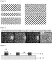
- the metal mesh pattern according to the exemplary embodiment of the present application is schematically illustrated in the following FIG. 5
- a metal mesh pattern in the related art is schematically illustrated in the following FIG. 6 .
- a line width 80, a line height 90, and a pitch 100 of the metal mesh pattern according to the exemplary embodiment of the present application are schematically illustrated in the following FIG. 8 .
- the line width, the line height, and the pitch of the metal mesh pattern may be measured by using a method known in the technical field. For example, a method of observing and measuring an SEM cross section, a measurement method using a non-contact surface shape measurer (optical profiler), a measurement method using a stylus surface profilometer (Alpha-Step or Surfacer Profiler), or the like may be used.
- the metal mesh patterns of the first common electrode wiring portion, the second common electrode wiring portion, and the signal electrode wiring portion may be formed by independent printing processes, respectively, or may be formed simultaneously by one printing process. Therefore, the metal mesh patterns of the first common electrode wiring portion, the second common electrode wiring portion, and the signal electrode wiring portion may have the same line width, the same pitch, and the same line height.
- the metal mesh patterns of the first common electrode wiring portion, the second common electrode wiring portion, and the signal electrode wiring portion may be formed on the transparent substrate.
- a printing method such as offset printing, screen printing, gravure printing, flexo-printing, inkjet printing, and nano-imprinting may be used as the printing method, but the printing method is not particularly limited, and a combination of the one or more methods may also be used.
- a roll-to-roll method, a roll-to-plate method, a plate-to-roll method, or a plate-to-plate method may be used as the printing method.
- a reverse offset printing method may be applied to implement a precise metal mesh pattern.
- a method may be performed in which ink, which may serve as a resist at the time of performing etching, is applied entirely onto the silicone-based rubber called a blanket, unnecessary parts are primarily removed by using an intaglio plate with a carved pattern called a cliche, the printed pattern remaining on the blanket is secondarily transferred onto a substrate such as a film or glass on which metal or the like is deposited, and then the transferred pattern is subjected to a firing process and an etching process to form a desired pattern.
- the printing method may comprise a direct printing method of forming a desired pattern by directly printing and then firing conductive ink by using the aforementioned reverse offset printing method.
- the line height of the pattern is flattened by pressing pressure, and conductivity may be imparted by a heat firing process, a microwave firing process, a laser partially firing process, or the like that makes connection made by mutual surface fusion of metal nanoparticles.
- a glass substrate or a plastic substrate which is known in the technical field, may be used as the transparent substrate, but the transparent substrate is not particularly limited.
- the light emitting element provided on the transparent substrate may be formed by using a material and a method known in the technical field.
- the Cu wiring pattern was formed to have the structure illustrated in the following FIG.
- a line width, a pitch, a line height, a width of a disconnected portion, and the like of the Cu wiring pattern are shown in the following Table 1.
- a standard deviation of the line width, the pitch, the line height, the width of the disconnected portion, and the like of the Cu wiring pattern was 2% or less.
- Low-temperature solder paste was printed onto an electrode pad portion by screen printing, and then LEDs were mounted on the solder paste. Thereafter, a solder paste reflow process was performed at about 170°C, such that metal in the solder paste bound and bonded the electrode pad portion and an LED pad portion.
- the wiring recognition was determined based on recognition of disconnection and channel with the naked eye at a spacing distance of 30 cm.
- the LED lighting was determined based on lighting of all of the 484 LEDs in a sheet of 0.5 m ⁇ 0.5 m, the LED lighting was evaluated as OK when all of the 484 LEDs were turned on, and the LED lighting was evaluated as NG when there were the LEDs that were not turned on.
- FIG. 7 An image operated by the transparent light emitting element display according to the exemplary embodiment of the present application is schematically illustrated in the following FIG. 7 .
- the transmittance was measured by using COH-400 of Nippon Denshoku Industries Co., Ltd.
- Comparative Example 1 was manufactured in the same manner as Experimental Example 1 except that electrode wiring was separately formed in the respective LEDs in Experimental Example 1.
- a line width, a pitch, a line height, a width of a disconnected portion, and the like of the Cu wiring pattern of Comparative Example 1 are shown in the following Table 2.
- Experimental Example 1 Comparative Example 1 Line Width ( ⁇ m) 20 20 Pitch ( ⁇ m) 200 200 Aperture Ratio (%) 81 84 Line Height ( ⁇ m) 5 5 Width of Disconnected Portion ( ⁇ m) 30 30 Linear Resistance ( ⁇ ) 1 12 Electrode Width (mm) 20 1.74 Electrode Length (mm) 440 460 LED Lighting OK NG
- the linear resistance was measured based on electrode wiring resistance to the last LED in a column in a power supply unit.
- the electrode width (interval between LEDs) of 20 mm is maintained to the last LED in Experimental Example 1, but in a case in which electrode wiring is formed in the respective LEDs in Comparative Example 1, the wiring width of the last LED in the column is reduced to 1.74 mm because the electrode width is divided and distributed to equalize resistance to the respective LEDs.
- the electrode length to the last LED is 440 mm in Experimental Example 1 because the 22 LEDs are disposed at an interval of 20 mm in the single column, while the electrode length is 460 mm in Comparative Example 1 because the interval of 20 mm between the LEDs is added to 440 mm.
- the metal mesh patterns which have the same line width, the same line height, and the same pitch, are applied to the first common electrode wiring portion, the second common electrode wiring portion, and the signal electrode wiring portion, it is possible to reduce wiring recognition.
- the metal mesh patterns are provided within the entire region of the effective screen portion on the upper surface of the transparent substrate except for the region in which the light emitting element is provided, it is possible to reduce resistance by maximizing the areas of the common electrode wiring portions.
Landscapes
- Electroluminescent Light Sources (AREA)
- Devices For Indicating Variable Information By Combining Individual Elements (AREA)
- Led Device Packages (AREA)
- Non-Insulated Conductors (AREA)
Abstract
Description
- This application claims priority to and the benefit of Korean Patent Application No.
10-2017-0096101 - The present application relates to a transparent light emitting element display.
- Recently in Korea, various types of scenery lighting as well as gorgeous signboards are created in parks and downtowns through fusion of cutting-edge ICT technologies and cutting-edge LED technologies, thereby providing urban residents with information and spectacles. In particular, a transparent LED display made of a transparent electrode material is configured by applying the LED between glass and glass and has an advantage in that luxurious appearances may be created because no electric wire is visible. For this reason, the transparent LED display is utilized for interior decoration in hotels, department stores, and the like and increases in importance in implementing media facades of outer walls of buildings.
- Demands for transparent electrodes, which are transparent, allow electricity to flow therethrough, and thus are used for touch screens or the like, are exponentially increased as smart devices come into wide use, and the most widely used transparent electrode, among the transparent electrodes, is indium tin oxide (ITO) which is oxide of indium and tin. However, the indium, which is a main ingredient of the ITO transparent electrode material, is produced only in some countries such as China, there is a small amount of indium reserves globally, and a large amount of costs are required to produce the indium. In addition, the indium has a high and inconsistent resistance value and thus has a disadvantage in that emitted LED light cannot exhibit desired and constant brightness. For this reason, there is a limitation in that the transparent LED utilizing the ITO cannot be utilized as a high-performance and low-priced transparent electrode material.
- The ITO, in fact, has been used as the transparent electrode material with the largest market share, but due to a limitation in terms of economic feasibility, restrictive performance, and the like, researches and technology development, which utilize new materials, are being consistently conducted. There are metal meshes, nanowires (Ag nanowires), carbon nanotubes (CNTs), conductive polymers, graphene, and the like as transparent electrode materials that attract the attention as next-generation materials. Among the materials, the metal mesh is a new material that occupies 85% of the materials substituted for the ITO, and the metal mesh is low in price and has high conductivity, such that the market related to the metal mesh expands in view of utilization.
- A transparent LED display, which utilizes the metal mesh, has much better conductivity than a transparent display in the related art, makes it easy to perform maintenance, saves resources, greatly reduces environmental pollution, and has economic feasibility resulting from a reduction in manufacturing costs. In addition, the metal mesh may be widely applied for various purposes and may be likely to be applied and utilized as a new transparent electrode material for various products.
- The present application has been made an effort to provide a transparent light emitting element display using a metal mesh pattern.
- An exemplary embodiment of the present application provides a transparent light emitting element display comprising: a transparent substrate; at least one light emitting element which is provided on the transparent substrate; and a first common electrode wiring portion, a second common electrode wiring portion, and a signal electrode wiring portion which are provided on the transparent substrate, in which all of the first common electrode wiring portion, the second common electrode wiring portion, and the signal electrode wiring portion comprise metal mesh patterns, respectively, each of the metal mesh patterns, which constitute the first common electrode wiring portion, the second common electrode wiring portion, and the signal electrode wiring portion, has a standard deviation of a line width which is 20% or less, a standard deviation of a pitch which is 10% or less, and a standard deviation of a line height which is 10% or less, and the metal mesh patterns are provided in a region having an area of 80% or more of an overall area on the transparent substrate.
- According to the exemplary embodiment of the present application, the metal mesh patterns, which have the same line width, the same line height, and the same pitch, are applied to the first common electrode wiring portion, the second common electrode wiring portion, and the signal electrode wiring portion, and as a result, it is possible to reduce wiring recognition. In addition, since the metal mesh patterns are provided within the entire region of the effective screen portion on the transparent substrate except for the region in which the light emitting element is provided, it is possible to reduce resistance by maximizing the areas of the common electrode wiring portions.
- In addition, according to the exemplary embodiment of the present application, it is possible to reduce wiring recognition by minimizing the widths of the disconnected portions that separate the metal mesh patterns of the first common electrode wiring portion, the second common electrode wiring portion, and the signal electrode wiring portion.
-
-
FIG. 1 is a view schematically illustrating electrode wiring of a transparent light emitting element display according to an exemplary embodiment of the present application. -
FIG. 2 is a view schematically illustrating signal transmission between electrodes and a flow of a power supply in the transparent light emitting element display according to the exemplary embodiment of the present application. -
FIGS. 3 and4 are views each schematically illustrating an electrode pad portion of the transparent light emitting element display according to the exemplary embodiment of the present application. -
FIG. 5 is a view schematically illustrating a metal mesh pattern according to the exemplary embodiment of the present application. -
FIG. 6 is a view schematically illustrating a metal mesh pattern in the related art. -
FIG. 7 is a view schematically illustrating an image operated by the transparent light emitting element display according to the exemplary embodiment of the present application. -
FIG. 8 is a view schematically illustrating a line width, a line height, and a pitch of the metal mesh pattern according to the exemplary embodiment of the present application. -
- 10:
- First common electrode wiring portion
- 20:
- Second common electrode wiring portion
- 30:
- Light emitting element
- 40:
- Power supply unit
- 50:
- Signal electrode wiring portion
- 60:
- Disconnected portion
- 70:
- Metal mesh pattern
- 80:
- Line width of metal mesh pattern
- 90:
- Line height of metal mesh pattern
- 100:
- Pitch of metal mesh pattern
- 110:
- Transparent substrate
- Hereinafter, the present application will be described in detail.
- A transparent LED display provides urban residents with various spectacles by providing information service and creating sceneries, and demands for the transparent LED display are increased in various fields. The ITO, in fact, has been used up to now as the transparent electrode material with the largest market share, but due to a limitation in terms of economic feasibility, restrictive performance, and the like, researches and technology development, which utilize new materials, are being consistently conducted.
- More specifically, transparent electrode wiring was formed by using Ag nanowires or transparent metal oxide (ITO, IZO, etc.) in order to implement a transparent LED display in the related art. However, because the Ag nanowire or the transparent metal oxide (ITO, IZO, etc.) has high resistance, the number of operating LEDs is restricted, and as a result, there is a limitation in increasing an area of the transparent LED display. In addition, in a case in which a thickness of the Ag nanowire or the transparent metal oxide is increased to reduce the resistance, there occurs a problem that transmittance of the transparent LED display deteriorates.
- Therefore, the present application is characterized by applying a metal mesh pattern to transparent electrode wiring of a transparent light emitting element display in order to provide the transparent light emitting element display having excellent resistance properties and visibility.
- A transparent light emitting element display according to an exemplary embodiment of the present application comprises: a transparent substrate; at least one light emitting element which is provided on the transparent substrate; and a first common electrode wiring portion, a second common electrode wiring portion, and a signal electrode wiring portion which are provided on the transparent substrate, in which all of the first common electrode wiring portion, the second common electrode wiring portion, and the signal electrode wiring portion comprise metal mesh patterns, respectively, each of the metal mesh patterns, which constitute the first common electrode wiring portion, the second common electrode wiring portion, and the signal electrode wiring portion, has a standard deviation of a line width which is 20% or less, a standard deviation of a pitch which is 10% or less, and a standard deviation of a line height which is 10% or less, and the metal mesh patterns are provided in a region having an area of 80% or more of an overall area on the transparent substrate.
- In the exemplary embodiment of the present application, at least four electrode pad portions, which electrically connect the light emitting element with the first common electrode wiring portion, the second common electrode wiring portion, and the signal electrode wiring portion, may be provided between the transparent substrate and the light emitting element. In this case, as illustrated in
FIGS. 3 and4 to be described below, no metal mesh pattern may be provided within at least a part of a region between the at least four electrode pad portions. - In the exemplary embodiment of the present application, two or more light emitting elements may be provided on the transparent substrate, and the two or more light emitting elements may be connected in series to the signal electrode wiring portion. The number of light emitting elements is not particularly limited and may be appropriately selected by those skilled in the art in consideration of the purpose or the like of the transparent light emitting element display. More specifically, the number of light emitting elements is related to resistance of an electrode, and the number of light emitting elements may be increased if the electrode has sufficiently low resistance and the display has a large area. Resolution is increased if the number of light emitting elements is increased in a state in which the area remains the same, and the area of the display is increased if the number of light emitting elements is increased in a state in which the interval remains the same, such that an electric wire line of an electric power supply unit may be reduced, and as a result, the number of light emitting elements may be appropriately selected by those skilled in the art in consideration of the purpose or the like of the transparent light emitting element display.
- In the exemplary embodiment of the present application, the two or more light emitting elements may be connected in series to the signal electrode wiring portion and connected in series to the first common electrode wiring portion and the second common electrode wiring portion. The first common electrode wiring portion and the second common electrode wiring portion provide the amount of electric current sufficient to operate the light emitting element, and the light emitting element may be connected in series to the signal electrode wiring portion because it is possible to send a signal with only a low electric current when sending a color signal of the light emitting element. If the respective electrodes are connected in parallel to the power supply unit to operate all of the light emitting elements and send a signal unlike the structure in the present application, all of the respective electrode widths need to be different from one another to adjust a resistance value in accordance with an arrangement distance between the light emitting elements (the electrode connected to the farthest light emitting element has the largest width), and it is difficult to implement a low-resistance electrode due to a spatial restriction to an electrode arrangement region because the multiple light emitting elements are provided.
- In the exemplary embodiment of the present application, the signal electrode wiring portion may be provided between the first common electrode wiring portion and the second common electrode wiring portion.
- In the exemplary embodiment of the present application, the first common electrode wiring portion may be a (+) common electrode wiring portion, and the second common electrode wiring portion may be a (-) common electrode wiring portion. In addition, the first common electrode wiring portion may be a (-) common electrode wiring portion, and the second common electrode wiring portion may be a (+) common electrode wiring portion.
- The electrode wiring of the transparent light emitting element display according to the exemplary embodiment of the present application is schematically illustrated in the following
FIG. 1 . - According to the exemplary embodiment of the present application, a channel is formed to have a structure in which the signal electrode wiring portion passes between the (+) common electrode wiring portion and the (-) common electrode wiring portion, such that the electrode wiring is not extended for each light emitting element and may be connected, as a common electrode, to the (+) common electrode wiring portion and the (-) common electrode wiring portion. Signal transmission between electrodes and a flow of a power supply in the transparent light emitting element display according to the exemplary embodiment of the present application is schematically illustrated in the following
FIG. 2 . - In the exemplary embodiment of the present application, at least four electrode pad portions, which electrically connect the light emitting element with the first common electrode wiring portion, the second common electrode wiring portion, and the signal electrode wiring portion, may be provided between the transparent substrate and the light emitting element. According to the exemplary embodiment of the present application, four electrode pad portions, which connect the light emitting element with the first common electrode wiring portion, the second common electrode wiring portion, and the signal electrode wiring portion, may be provided between the transparent substrate and the light emitting element.
- In the exemplary embodiment of the present application, the four electrode pad portions may comprise two signal electrode pad portions, one first common electrode pad portion, and one second common electrode pad portion. The two signal electrode pad portions are signal in-out pad portions for a light emitting element and may be provided at ends of the signal electrode wiring portions, respectively, and the first common electrode pad portion and the second common electrode pad portion may be provided at an end of the first common electrode wiring portion and an end of the second common electrode wiring portion, respectively. The ends mean regions in which the light emitting element is provided at an upper side thereof and the first common electrode wiring portion, the second common electrode wiring portion, and the signal electrode wiring portion are electrically connected to the light emitting element.
- In addition, at least one capacitor pad portion may be additionally comprised on the transparent substrate. In the exemplary embodiment of the present application, the number of capacitor pad portions may be two.
- The capacitor pad portion is a pad to which a capacitor is attached, and the capacitor may serve to stabilize an electric current to be supplied to the light emitting element.
- The following
FIGS. 3 and4 are views each schematically illustrating an electrode pad portion of the transparent light emitting element display according to the exemplary embodiment of the present application.FIGS. 3 and4 are views illustrating a case in which four electrode pad portions and two capacitor pad portions are provided. - More specifically, in
FIGS. 3 and4 , part A illustrates a (+) common electrode wiring portion, part B illustrates a (-) common electrode wiring portion, and part C illustrates a signal electrode wiring portion. In addition, inFIGS. 3 and4 ,electrode pad portions electrode pad portion 3 is a (+) pad portion of the light emitting element, that is, an electrode pad portion provided to be connected to an end of the (+) common electrode wiring portion, and anelectrode pad portion 4 is a (-) pad portion of the light emitting element, that is, an electrode pad portion provided to be connected to an end of the (-) common electrode wiring portion. In addition, acapacitor pad portion 5 is a capacitor (+) pad portion, and acapacitor pad portion 6 is a capacitor (-) pad portion. - Parts A, B, and C comprise metal mesh patterns, and no metal mesh pattern is provided between the
electrode pad portions 1 to 4. In addition, theelectrode pad portions 1 to 4 and thecapacitor pad portions - Intervals between the electrode pad portions and the capacitor pad portions may be each independently 0.1 mm to 1 mm. With the aforementioned intervals, it is possible to prevent a short-circuit in consideration of a tolerance when performing screen printing with solder paste for forming the light emitting element later.
- The shape of each of the electrode pad portions and the capacitor pad portions is not particularly limited and may be a quadrangular shape. In addition, a size of each of the electrode pad portions and the capacitor pad portions may be, but not limited only to, 0.1 mm2 to 1 mm2.
- The four electrode pad portions may be joined to one light emitting element. That is, in the exemplary embodiment of the present application, in a case in which multiple light emitting elements are provided on a transparent substrate, the respective light emitting elements may be joined to the four electrode pad portions.
- In the exemplary embodiment of the present application, the first common electrode wiring portion, the second common electrode wiring portion, and the signal electrode wiring portion may comprise metal mesh patterns, respectively, which have the same line width, the same line height, and the same pitch. In the present application, the configuration in which the metal mesh patterns have the same line width means that a standard deviation of the line width is 20% or less, particularly, 10% or less, and more particularly, 5% or less. In addition, in the present application, the configuration in which the metal mesh patterns have the same line height means that a standard deviation of the line height is 10% or less, particularly, 5% or less, and more particularly, 2% or less. In addition, in the present application, the configuration in which the metal mesh patterns have the same pitch means that a standard deviation of the pitch is 10% or less, particularly, 5% or less, and more particularly, 2% or less.
- In the exemplary embodiment of the present application, the metal mesh patterns may be provided within the entire region of an effective screen portion on the transparent substrate except for the region in which the light emitting element is provided. More specifically, the metal mesh patterns may be provided within a region having an area of 80% or more and 99.5% or less of an overall area on the transparent substrate. In addition, based on the overall area on the transparent substrate, the metal mesh patterns may be provided within a region having an area of 80% or more and 99.5% or less of an area of a region except for an FPCB pad portion region and a light emitting element pad portion region provided on the transparent substrate. In the present application, the FPCB pad portion region may comprise an FPCB pad portion for applying external power, and an area of the FPCB pad portion region may be equal to or larger than an overall area of the FPCB pad portion and equal to or smaller than 3 times the overall area of the FPCB pad portion. In addition, in the present application, the light emitting element pad portion region comprises the electrode pad portions, and an area of the light emitting element pad portion region may be equal to or larger than 1.5 times the overall area of the electrode pad portions and equal to or smaller than 3 times the overall area of the electrode pad portions.
- In the exemplary embodiment of the present application, the metal mesh pattern may satisfy the following
Expression 1.
- In
Expression 1, P represents the pitch of the metal mesh pattern, and W represents the line width of the metal mesh pattern. - In the exemplary embodiment of the present application, pattern shapes in the technical field may be used as the metal mesh patterns of the first common electrode wiring portion, the second common electrode wiring portion, and the signal electrode wiring portion. More specifically, the metal mesh pattern may comprise a polygonal pattern having one or more shapes of a triangle, a quadrilateral, a pentagon, a hexagon, and an octagon.
- The metal mesh pattern may comprise a straight line, a curve, or a closed curve formed of a straight line or a curve.
- Since the metal mesh patterns may be provided within the entire region of the effective screen portion of the upper surface of the transparent substrate except for the region in which the light emitting element is provided, it is possible to obtain a maximally acceptable wiring region, and thus it is possible to improve resistance properties of the transparent light emitting element display. More specifically, surface resistance of the metal mesh pattern may be 0.1 Ω/sq or less.
- The pitch of the metal mesh pattern may be 100 µm to 1,000 µm, 100 µm to 600 µm, or 100 µm to 300 µm, but the pitch of the metal mesh pattern may be adjusted by those skilled in the art in accordance with desired transmittance and conductivity.
- A material of the metal mesh pattern is not particularly limited, but may comprise one or more types of metal and metal alloys. The metal mesh pattern may comprise, but not limited only to, gold, silver, aluminum, copper, neodymium, molybdenum, nickel, or an alloy thereof.
- The line height of the metal mesh pattern is not particularly limited, but may be 3 µm or more and 20 µm or less or 10 µm or less in terms of conductivity of the metal mesh pattern and economic feasibility of a forming process. More specifically, the line height of the metal mesh pattern may be 3 µm to 20 µm, or 3 µm to 10 µm.
- The line width of the metal mesh pattern may be, but not limited only to, 50 µm or less, 25 µm or less, or 20 µm or less. The smaller line width of the metal mesh pattern may be advantageous in terms of transmittance and wiring recognition but may cause a reduction in resistance, and in this case, the reduction in resistance may be improved by increasing the line height of the metal mesh pattern. The line width of the metal mesh pattern may be 5 µm or more.
- An aperture ratio of the metal mesh pattern, that is, a ratio of an area, which is not covered by the pattern, may be 70% or more, 85% or more, or 95% or more.
- According to the exemplary embodiment of the present application, the metal mesh patterns, which have the same line width, the same line height, and the same pitch, are applied to the first common electrode wiring portion, the second common electrode wiring portion, and the signal electrode wiring portion, and as a result, it is possible to reduce wiring recognition. If the metal mesh patterns of the first common electrode wiring portion, the second common electrode wiring portion, and the signal electrode wiring portion do not have the same line width, the same pitch, or the same line height, recognition of the wiring portions may be increased, which is not preferable.
- In the exemplary embodiment of the present application, the metal mesh patterns of the first common electrode wiring portion, the second common electrode wiring portion, and the signal electrode wiring portion may be separated from one another by disconnected portions where no metal mesh pattern is provided. The disconnected portion means a region in which a part of the metal mesh pattern is disconnected and electrical connection is disconnected. A width of the disconnected portion may mean a distance between nearest ends of the first common electrode wiring portion, the second common electrode wiring portion, and the signal electrode wiring portion which are spaced apart from one another. A width of the disconnected portion may be, but not limited only to, 80 µm or less, 60 µm or less, 40 µm or less, or 30 µm or less. The width of the disconnected portion may be 5 µm or more.
- The metal mesh pattern according to the exemplary embodiment of the present application is schematically illustrated in the following
FIG. 5 , and a metal mesh pattern in the related art is schematically illustrated in the followingFIG. 6 . - In addition, a
line width 80, aline height 90, and apitch 100 of the metal mesh pattern according to the exemplary embodiment of the present application are schematically illustrated in the followingFIG. 8 . The line width, the line height, and the pitch of the metal mesh pattern may be measured by using a method known in the technical field. For example, a method of observing and measuring an SEM cross section, a measurement method using a non-contact surface shape measurer (optical profiler), a measurement method using a stylus surface profilometer (Alpha-Step or Surfacer Profiler), or the like may be used. - According to the exemplary embodiment of the present application, it is possible to reduce wiring recognition by minimizing the widths of the disconnected portions that separate the metal mesh patterns of the first common electrode wiring portion, the second common electrode wiring portion, and the signal electrode wiring portion.
- In the exemplary embodiment of the present application, the metal mesh patterns of the first common electrode wiring portion, the second common electrode wiring portion, and the signal electrode wiring portion may be formed by independent printing processes, respectively, or may be formed simultaneously by one printing process. Therefore, the metal mesh patterns of the first common electrode wiring portion, the second common electrode wiring portion, and the signal electrode wiring portion may have the same line width, the same pitch, and the same line height.
- In the exemplary embodiment of the present application, since a printing method is used to form the metal mesh patterns of the first common electrode wiring portion, the second common electrode wiring portion, and the signal electrode wiring portion, the metal mesh patterns of the first common electrode wiring portion, the second common electrode wiring portion, and the signal electrode wiring portion, which have thin and precise line widths, may be formed on the transparent substrate. A printing method such as offset printing, screen printing, gravure printing, flexo-printing, inkjet printing, and nano-imprinting may be used as the printing method, but the printing method is not particularly limited, and a combination of the one or more methods may also be used. A roll-to-roll method, a roll-to-plate method, a plate-to-roll method, or a plate-to-plate method may be used as the printing method.
- In the exemplary embodiment of the present application, a reverse offset printing method may be applied to implement a precise metal mesh pattern. To this end, in the present application, a method may be performed in which ink, which may serve as a resist at the time of performing etching, is applied entirely onto the silicone-based rubber called a blanket, unnecessary parts are primarily removed by using an intaglio plate with a carved pattern called a cliche, the printed pattern remaining on the blanket is secondarily transferred onto a substrate such as a film or glass on which metal or the like is deposited, and then the transferred pattern is subjected to a firing process and an etching process to form a desired pattern. In this method, since the substrate on which metal is deposited is used, uniformity of the line height is ensured within the entire region, such that there is an advantage in that resistance in a thickness direction may be uniformly maintained. In addition, in the present application, the printing method may comprise a direct printing method of forming a desired pattern by directly printing and then firing conductive ink by using the aforementioned reverse offset printing method. In this case, the line height of the pattern is flattened by pressing pressure, and conductivity may be imparted by a heat firing process, a microwave firing process, a laser partially firing process, or the like that makes connection made by mutual surface fusion of metal nanoparticles.
- In the exemplary embodiment of the present application, a glass substrate or a plastic substrate, which is known in the technical field, may be used as the transparent substrate, but the transparent substrate is not particularly limited.
- In the exemplary embodiment of the present application, the light emitting element provided on the transparent substrate may be formed by using a material and a method known in the technical field.
- Hereinafter, the exemplary embodiments described in the present specification will be exemplified through Examples. However, it is not intended that the scopes of the exemplary embodiments are limited by the following Examples.
- A raw material made by plating a transparent film (Polyester Film V7200 of SKC) with Cu and a dry film resist (DFR, SPG-152 of Asahi Chemical Industry) were laminated. Thereafter, exposure was performed in a state in which a pattern mask was attached thereto, and then development was performed, such that a desired DFR pattern was formed. Thereafter, Cu etching and DFR separation were performed to manufacture a desired Cu wiring pattern (the Cu wiring pattern was provided within a region having an area of 80% or more of the entire area on the transparent film). The Cu wiring pattern was formed to have the structure illustrated in the following
FIG. 3 , and a line width, a pitch, a line height, a width of a disconnected portion, and the like of the Cu wiring pattern are shown in the following Table 1. A standard deviation of the line width, the pitch, the line height, the width of the disconnected portion, and the like of the Cu wiring pattern was 2% or less. - Low-temperature solder paste was printed onto an electrode pad portion by screen printing, and then LEDs were mounted on the solder paste. Thereafter, a solder paste reflow process was performed at about 170°C, such that metal in the solder paste bound and bonded the electrode pad portion and an LED pad portion.
[Table 1] Experimental Example 1 Experimental Example 2 Experimental Example 3 Experimental Example 4 Line Width (µm) 20 20 20 30 Pitch (µm) 200 200 200 200 Aperture Ratio (%) 81 81 81 72 Line Height (µm) 5 2 5 5 Width of Disconnected Portion (µm) 30 30 100 30 Resistance (Ω/sq) 0.045 0.110 0.045 0.03 Wiring Recognition OK OK NG OK Transmittance (%) 72 72 72 63 LED Lighting OK NG OK OK - The wiring recognition was determined based on recognition of disconnection and channel with the naked eye at a spacing distance of 30 cm.
- The LED lighting was determined based on lighting of all of the 484 LEDs in a sheet of 0.5 m × 0.5 m, the LED lighting was evaluated as OK when all of the 484 LEDs were turned on, and the LED lighting was evaluated as NG when there were the LEDs that were not turned on.
- An image operated by the transparent light emitting element display according to the exemplary embodiment of the present application is schematically illustrated in the following
FIG. 7 . - The transmittance was measured by using COH-400 of Nippon Denshoku Industries Co., Ltd.
- Comparative Example 1 was manufactured in the same manner as Experimental Example 1 except that electrode wiring was separately formed in the respective LEDs in Experimental Example 1. A line width, a pitch, a line height, a width of a disconnected portion, and the like of the Cu wiring pattern of Comparative Example 1 are shown in the following Table 2.
[Table 2] Experimental Example 1 Comparative Example 1 Line Width (µm) 20 20 Pitch (µm) 200 200 Aperture Ratio (%) 81 84 Line Height (µm) 5 5 Width of Disconnected Portion (µm) 30 30 Linear Resistance (Ω) 1 12 Electrode Width (mm) 20 1.74 Electrode Length (mm) 440 460 LED Lighting OK NG - The linear resistance was measured based on electrode wiring resistance to the last LED in a column in a power supply unit.
- The electrode width (interval between LEDs) of 20 mm is maintained to the last LED in Experimental Example 1, but in a case in which electrode wiring is formed in the respective LEDs in Comparative Example 1, the wiring width of the last LED in the column is reduced to 1.74 mm because the electrode width is divided and distributed to equalize resistance to the respective LEDs.
- The electrode length to the last LED is 440 mm in Experimental Example 1 because the 22 LEDs are disposed at an interval of 20 mm in the single column, while the electrode length is 460 mm in Comparative Example 1 because the interval of 20 mm between the LEDs is added to 440 mm.
- As seen in the results, according to the exemplary embodiment of the present application, since the metal mesh patterns, which have the same line width, the same line height, and the same pitch, are applied to the first common electrode wiring portion, the second common electrode wiring portion, and the signal electrode wiring portion, it is possible to reduce wiring recognition. In addition, since the metal mesh patterns are provided within the entire region of the effective screen portion on the upper surface of the transparent substrate except for the region in which the light emitting element is provided, it is possible to reduce resistance by maximizing the areas of the common electrode wiring portions.
- In addition, according to the exemplary embodiment of the present application, it is possible to reduce wiring recognition by minimizing the widths of the disconnected portions that separate the metal mesh patterns of the first common electrode wiring portion, the second common electrode wiring portion, and the signal electrode wiring portion.
Claims (13)
- A transparent light emitting element display comprising:a transparent substrate;at least one light emitting element which is provided on the transparent substrate; anda first common electrode wiring portion, a second common electrode wiring portion, and a signal electrode wiring portion which are provided on the transparent substrate,wherein all of the first common electrode wiring portion, the second common electrode wiring portion, and the signal electrode wiring portion comprise metal mesh patterns, respectively,each of the metal mesh patterns, which constitute the first common electrode wiring portion, the second common electrode wiring portion, and the signal electrode wiring portion, has a standard deviation of a line width which is 20% or less, a standard deviation of a pitch which is 10% or less, and a standard deviation of a line height which is 10% or less, andthe metal mesh patterns are provided in a region having an area of 80% or more of an overall area on the transparent substrate.
- The transparent light emitting element display of claim 1, wherein at least four electrode pad portions, which electrically connect the light emitting element with the first common electrode wiring portion, the second common electrode wiring portion, and the signal electrode wiring portion, are provided between the transparent substrate and the light emitting element.
- The transparent light emitting element display of claim 2, wherein the at least four electrode pad portions comprise two signal electrode pad portions, one first common electrode pad portion, and one second common electrode pad portion.
- The transparent light emitting element display of claim 1, wherein the two or more light emitting elements are provided, and the two or more light emitting elements are connected in series to the signal electrode wiring portion.
- The transparent light emitting element display of claim 1, wherein the signal electrode wiring portion is provided between the first common electrode wiring portion and the second common electrode wiring portion.
- The transparent light emitting element display of claim 1, wherein the metal mesh pattern satisfies the following Expression 1,

- The transparent light emitting element display of claim 1, wherein surface resistance of the metal mesh pattern is 0.1 Ω/sq or less.
- The transparent light emitting element display of claim 1, wherein the line width of the metal mesh pattern is 50 µm or less, the pitch of the metal mesh pattern is 100 µm to 1,000 µm, and the line height of the metal mesh pattern is 3 µm or more.
- The transparent light emitting element display of claim 1, wherein the metal mesh patterns of the first common electrode wiring portion, the second common electrode wiring portion, and the signal electrode wiring portion are separated from one another by disconnected portions, respectively, where no metal mesh pattern is provided, and a width of the disconnected portion is 80 µm or less.
- The transparent light emitting element display of claim 2, wherein sizes of the electrode pad portions are each independently 0.1 mm2 to 1 mm2.
- The transparent light emitting element display of claim 2, wherein intervals between the at least four electrode pad portions are each independently 0.1 mm to 1 mm.
- The transparent light emitting element display of claim 1, wherein the metal mesh pattern comprises gold, silver, aluminum, copper, neodymium, molybdenum, nickel, or an alloy thereof.
- The transparent light emitting element display of claim 1, further comprising:
at least one capacitor pad portion on the transparent substrate.
Applications Claiming Priority (2)
| Application Number | Priority Date | Filing Date | Title |
|---|---|---|---|
| KR20170096101 | 2017-07-28 | ||
| PCT/KR2018/008407 WO2019022500A1 (en) | 2017-07-28 | 2018-07-25 | Transparent light emitting element display |
Publications (3)
| Publication Number | Publication Date |
|---|---|
| EP3660903A1 true EP3660903A1 (en) | 2020-06-03 |
| EP3660903A4 EP3660903A4 (en) | 2020-08-12 |
| EP3660903B1 EP3660903B1 (en) | 2022-02-09 |
Family
ID=65040641
Family Applications (1)
| Application Number | Title | Priority Date | Filing Date |
|---|---|---|---|
| EP18837540.6A Active EP3660903B1 (en) | 2017-07-28 | 2018-07-25 | Transparent light emitting element display |
Country Status (7)
| Country | Link |
|---|---|
| US (1) | US10964869B2 (en) |
| EP (1) | EP3660903B1 (en) |
| JP (1) | JP7031816B2 (en) |
| KR (1) | KR102149083B1 (en) |
| CN (1) | CN110770909B (en) |
| TW (1) | TWI669699B (en) |
| WO (1) | WO2019022500A1 (en) |
Families Citing this family (10)
| Publication number | Priority date | Publication date | Assignee | Title |
|---|---|---|---|---|
| KR102116393B1 (en) * | 2019-02-27 | 2020-05-28 | (주) 글로우원 | Transparent LED display panel having double-sided electrodes |
| CN110033711B (en) * | 2019-03-28 | 2024-07-26 | 深圳市晶泓科技有限公司 | Transparent LED display screen |
| CN110246428A (en) * | 2019-06-19 | 2019-09-17 | 大连集思特科技有限公司 | High-density transparent LED display screen and manufacturing method thereof |
| KR102287177B1 (en) * | 2019-07-24 | 2021-08-06 | 한솔테크닉스(주) | Transparent light emitting device |
| KR102287837B1 (en) * | 2019-12-05 | 2021-08-10 | 주식회사 리페어코리아 | Plate for manufaturing a transparent display using metal mesh |
| CN111554204A (en) * | 2020-06-08 | 2020-08-18 | 深圳市海柏恩科技有限公司 | A high-contrast transparent LED display |
| TWM614583U (en) * | 2020-11-30 | 2021-07-21 | 范文正 | Light emitting display device |
| KR102497889B1 (en) * | 2022-06-15 | 2023-02-09 | 주식회사 루미디아 | Electrode substrate of transparent display panel and transparent display panel including the same |
| CN118303149A (en) * | 2022-11-03 | 2024-07-05 | 京东方科技集团股份有限公司 | Display substrate and transparent display device |
| US20250022855A1 (en) * | 2023-07-14 | 2025-01-16 | Seoul Semiconductor Co., Ltd. | Light emitting module and light emitting system including the same |
Family Cites Families (34)
| Publication number | Priority date | Publication date | Assignee | Title |
|---|---|---|---|---|
| JP2934662B2 (en) * | 1994-09-27 | 1999-08-16 | フーリエ有限会社 | Display device |
| WO1996010244A1 (en) | 1994-09-27 | 1996-04-04 | Shinsuke Nishida | Display |
| GB0220613D0 (en) * | 2002-09-05 | 2002-10-16 | Koninkl Philips Electronics Nv | Electroluminescent display devices |
| JP4610416B2 (en) | 2005-06-10 | 2011-01-12 | 日本写真印刷株式会社 | Capacitive touch panel |
| US8274494B2 (en) * | 2008-02-28 | 2012-09-25 | 3M Innovative Properties Company | Touch screen sensor having varying sheet resistance |
| CN201226216Y (en) * | 2008-05-15 | 2009-04-22 | 蓝星光电科技股份有限公司 | Light-transmitting display device containing LED and control logic circuit |
| JP5249806B2 (en) | 2009-02-16 | 2013-07-31 | グンゼ株式会社 | Touch switch |
| TWI550649B (en) * | 2009-07-16 | 2016-09-21 | Lg化學股份有限公司 | Electrical conductor and preparation method thereof |
| KR101105887B1 (en) * | 2010-04-26 | 2012-01-16 | (주)케이스원 | LED package mounting board and manufacturing method thereof |
| TWM403720U (en) * | 2010-09-03 | 2011-05-11 | Blue Star Lighting Technology Co Ltd | FPC type LED display device |
| US9046974B2 (en) * | 2012-02-28 | 2015-06-02 | Eastman Kodak Company | Transparent touch-screen capacitor with micro-wire electrode |
| JP5888255B2 (en) * | 2013-01-31 | 2016-03-16 | 大日本印刷株式会社 | Electrode film, method for producing the same, and image display device |
| KR102011435B1 (en) | 2013-03-07 | 2019-08-19 | 삼성디스플레이 주식회사 | Display Device Integrated Touch Screen Panel and Driving Method Thereof |
| US20150268756A1 (en) * | 2013-09-11 | 2015-09-24 | Ronald Steven Cok | Multi-area micro-wire structure |
| TW201512914A (en) | 2013-09-17 | 2015-04-01 | Wintek Corp | Touch control panel and touch display device |
| KR20150033169A (en) | 2013-09-23 | 2015-04-01 | 엘지디스플레이 주식회사 | Light emitting diode package and liquid crystal display device using the same |
| US20150378481A1 (en) * | 2014-06-25 | 2015-12-31 | Ronald Steven Cok | Micro-wire electrodes having different spatial resolutions |
| CN104103674B (en) | 2014-08-04 | 2017-04-12 | 石益坚 | Capacitive driving electroluminescence display and manufacturing method thereof |
| CN106030839B (en) | 2014-09-26 | 2018-09-28 | 东芝北斗电子株式会社 | Light emitting module |
| WO2016047133A1 (en) | 2014-09-26 | 2016-03-31 | 東芝ホクト電子株式会社 | Light-emission module |
| JP6418910B2 (en) | 2014-11-14 | 2018-11-07 | 三菱電機株式会社 | Touch screen, touch panel and display device |
| US9811464B2 (en) | 2014-12-11 | 2017-11-07 | Intel Corporation | Apparatus and method for considering spatial locality in loading data elements for execution |
| CN104837178A (en) | 2015-01-29 | 2015-08-12 | 小米科技有限责任公司 | Network accessing method and device |
| KR101747846B1 (en) | 2015-01-30 | 2017-06-15 | 금호전기주식회사 | Transparent light emitting apparatus |
| KR101784406B1 (en) * | 2015-02-25 | 2017-10-12 | 금호전기주식회사 | Transparent light emitting apparatus |
| TWI610204B (en) * | 2015-02-27 | 2018-01-01 | Fujikura Ltd | Wiring body, wiring board, and touch detector |
| JP6470833B2 (en) * | 2015-03-04 | 2019-02-13 | 富士フイルム株式会社 | Touch panel adhesive sheet, touch panel laminate, capacitive touch panel |
| CN104777939B (en) * | 2015-04-24 | 2018-01-16 | 昆山龙腾光电有限公司 | Contact panel |
| JP6633622B2 (en) | 2015-05-01 | 2020-01-22 | 東芝ホクト電子株式会社 | Light emitting module |
| US10133426B2 (en) * | 2015-06-18 | 2018-11-20 | X-Celeprint Limited | Display with micro-LED front light |
| KR101689131B1 (en) * | 2015-07-24 | 2016-12-23 | 케이알에코스타 주식회사 | Transparent Display Using Metal Mesh |
| US10834815B2 (en) * | 2015-12-01 | 2020-11-10 | Japan Aviation Electronics Industry, Limited | Printed wiring line, electronic device, touch panel, gravure plate, printed wiring line formation method, touch panel production method, and electronic device production method |
| JP6833722B2 (en) | 2015-12-28 | 2021-02-24 | 東芝ホクト電子株式会社 | Luminous module |
| CN106293200A (en) * | 2016-07-26 | 2017-01-04 | 京东方科技集团股份有限公司 | A kind of cover plate and preparation method thereof, display device |
-
2018
- 2018-07-25 KR KR1020180086621A patent/KR102149083B1/en active Active
- 2018-07-25 US US16/625,299 patent/US10964869B2/en active Active
- 2018-07-25 EP EP18837540.6A patent/EP3660903B1/en active Active
- 2018-07-25 WO PCT/KR2018/008407 patent/WO2019022500A1/en not_active Ceased
- 2018-07-25 JP JP2019571303A patent/JP7031816B2/en active Active
- 2018-07-25 CN CN201880040549.XA patent/CN110770909B/en active Active
- 2018-07-27 TW TW107126171A patent/TWI669699B/en active
Also Published As
| Publication number | Publication date |
|---|---|
| KR102149083B1 (en) | 2020-08-27 |
| EP3660903B1 (en) | 2022-02-09 |
| US10964869B2 (en) | 2021-03-30 |
| WO2019022500A1 (en) | 2019-01-31 |
| CN110770909B (en) | 2023-11-10 |
| US20200251637A1 (en) | 2020-08-06 |
| TW201911278A (en) | 2019-03-16 |
| KR20190013564A (en) | 2019-02-11 |
| TWI669699B (en) | 2019-08-21 |
| EP3660903A4 (en) | 2020-08-12 |
| JP2020524823A (en) | 2020-08-20 |
| JP7031816B2 (en) | 2022-03-08 |
| CN110770909A (en) | 2020-02-07 |
Similar Documents
| Publication | Publication Date | Title |
|---|---|---|
| EP3660903B1 (en) | Transparent light emitting element display | |
| KR102075272B1 (en) | Transparent light emitting device display | |
| KR102129674B1 (en) | Electrode substrate for transparent light emitting device display and method for manufacturing thereof | |
| EP3742491B1 (en) | Electrode substrate for transparent light-emitting diode display device, and transparent light-emitting diode display device comprising same | |
| KR102130215B1 (en) | Transparent light emitting device display |
Legal Events
| Date | Code | Title | Description |
|---|---|---|---|
| STAA | Information on the status of an ep patent application or granted ep patent |
Free format text: STATUS: THE INTERNATIONAL PUBLICATION HAS BEEN MADE |
|
| PUAI | Public reference made under article 153(3) epc to a published international application that has entered the european phase |
Free format text: ORIGINAL CODE: 0009012 |
|
| STAA | Information on the status of an ep patent application or granted ep patent |
Free format text: STATUS: REQUEST FOR EXAMINATION WAS MADE |
|
| 17P | Request for examination filed |
Effective date: 20191212 |
|
| AK | Designated contracting states |
Kind code of ref document: A1 Designated state(s): AL AT BE BG CH CY CZ DE DK EE ES FI FR GB GR HR HU IE IS IT LI LT LU LV MC MK MT NL NO PL PT RO RS SE SI SK SM TR |
|
| AX | Request for extension of the european patent |
Extension state: BA ME |
|
| REG | Reference to a national code |
Ref country code: DE Ref legal event code: R079 Ref document number: 602018030726 Country of ref document: DE Free format text: PREVIOUS MAIN CLASS: H01L0027150000 Ipc: H01L0025075000 |
|
| A4 | Supplementary search report drawn up and despatched |
Effective date: 20200709 |
|
| RIC1 | Information provided on ipc code assigned before grant |
Ipc: H01L 25/075 20060101AFI20200704BHEP Ipc: H01L 33/62 20100101ALI20200704BHEP |
|
| DAV | Request for validation of the european patent (deleted) | ||
| DAX | Request for extension of the european patent (deleted) | ||
| GRAP | Despatch of communication of intention to grant a patent |
Free format text: ORIGINAL CODE: EPIDOSNIGR1 |
|
| STAA | Information on the status of an ep patent application or granted ep patent |
Free format text: STATUS: GRANT OF PATENT IS INTENDED |
|
| INTG | Intention to grant announced |
Effective date: 20210928 |
|
| GRAS | Grant fee paid |
Free format text: ORIGINAL CODE: EPIDOSNIGR3 |
|
| GRAA | (expected) grant |
Free format text: ORIGINAL CODE: 0009210 |
|
| STAA | Information on the status of an ep patent application or granted ep patent |
Free format text: STATUS: THE PATENT HAS BEEN GRANTED |
|
| AK | Designated contracting states |
Kind code of ref document: B1 Designated state(s): AL AT BE BG CH CY CZ DE DK EE ES FI FR GB GR HR HU IE IS IT LI LT LU LV MC MK MT NL NO PL PT RO RS SE SI SK SM TR |
|
| REG | Reference to a national code |
Ref country code: GB Ref legal event code: FG4D |
|
| REG | Reference to a national code |
Ref country code: CH Ref legal event code: EP Ref country code: AT Ref legal event code: REF Ref document number: 1468032 Country of ref document: AT Kind code of ref document: T Effective date: 20220215 |
|
| REG | Reference to a national code |
Ref country code: IE Ref legal event code: FG4D |
|
| REG | Reference to a national code |
Ref country code: DE Ref legal event code: R096 Ref document number: 602018030726 Country of ref document: DE |
|
| REG | Reference to a national code |
Ref country code: LT Ref legal event code: MG9D |
|
| REG | Reference to a national code |
Ref country code: NL Ref legal event code: MP Effective date: 20220209 |
|
| REG | Reference to a national code |
Ref country code: AT Ref legal event code: MK05 Ref document number: 1468032 Country of ref document: AT Kind code of ref document: T Effective date: 20220209 |
|
| PG25 | Lapsed in a contracting state [announced via postgrant information from national office to epo] |
Ref country code: SE Free format text: LAPSE BECAUSE OF FAILURE TO SUBMIT A TRANSLATION OF THE DESCRIPTION OR TO PAY THE FEE WITHIN THE PRESCRIBED TIME-LIMIT Effective date: 20220209 Ref country code: RS Free format text: LAPSE BECAUSE OF FAILURE TO SUBMIT A TRANSLATION OF THE DESCRIPTION OR TO PAY THE FEE WITHIN THE PRESCRIBED TIME-LIMIT Effective date: 20220209 Ref country code: PT Free format text: LAPSE BECAUSE OF FAILURE TO SUBMIT A TRANSLATION OF THE DESCRIPTION OR TO PAY THE FEE WITHIN THE PRESCRIBED TIME-LIMIT Effective date: 20220609 Ref country code: NO Free format text: LAPSE BECAUSE OF FAILURE TO SUBMIT A TRANSLATION OF THE DESCRIPTION OR TO PAY THE FEE WITHIN THE PRESCRIBED TIME-LIMIT Effective date: 20220509 Ref country code: NL Free format text: LAPSE BECAUSE OF FAILURE TO SUBMIT A TRANSLATION OF THE DESCRIPTION OR TO PAY THE FEE WITHIN THE PRESCRIBED TIME-LIMIT Effective date: 20220209 Ref country code: LT Free format text: LAPSE BECAUSE OF FAILURE TO SUBMIT A TRANSLATION OF THE DESCRIPTION OR TO PAY THE FEE WITHIN THE PRESCRIBED TIME-LIMIT Effective date: 20220209 Ref country code: HR Free format text: LAPSE BECAUSE OF FAILURE TO SUBMIT A TRANSLATION OF THE DESCRIPTION OR TO PAY THE FEE WITHIN THE PRESCRIBED TIME-LIMIT Effective date: 20220209 Ref country code: ES Free format text: LAPSE BECAUSE OF FAILURE TO SUBMIT A TRANSLATION OF THE DESCRIPTION OR TO PAY THE FEE WITHIN THE PRESCRIBED TIME-LIMIT Effective date: 20220209 Ref country code: BG Free format text: LAPSE BECAUSE OF FAILURE TO SUBMIT A TRANSLATION OF THE DESCRIPTION OR TO PAY THE FEE WITHIN THE PRESCRIBED TIME-LIMIT Effective date: 20220509 |
|
| PG25 | Lapsed in a contracting state [announced via postgrant information from national office to epo] |
Ref country code: PL Free format text: LAPSE BECAUSE OF FAILURE TO SUBMIT A TRANSLATION OF THE DESCRIPTION OR TO PAY THE FEE WITHIN THE PRESCRIBED TIME-LIMIT Effective date: 20220209 Ref country code: LV Free format text: LAPSE BECAUSE OF FAILURE TO SUBMIT A TRANSLATION OF THE DESCRIPTION OR TO PAY THE FEE WITHIN THE PRESCRIBED TIME-LIMIT Effective date: 20220209 Ref country code: GR Free format text: LAPSE BECAUSE OF FAILURE TO SUBMIT A TRANSLATION OF THE DESCRIPTION OR TO PAY THE FEE WITHIN THE PRESCRIBED TIME-LIMIT Effective date: 20220510 Ref country code: FI Free format text: LAPSE BECAUSE OF FAILURE TO SUBMIT A TRANSLATION OF THE DESCRIPTION OR TO PAY THE FEE WITHIN THE PRESCRIBED TIME-LIMIT Effective date: 20220209 Ref country code: AT Free format text: LAPSE BECAUSE OF FAILURE TO SUBMIT A TRANSLATION OF THE DESCRIPTION OR TO PAY THE FEE WITHIN THE PRESCRIBED TIME-LIMIT Effective date: 20220209 |
|
| PG25 | Lapsed in a contracting state [announced via postgrant information from national office to epo] |
Ref country code: IS Free format text: LAPSE BECAUSE OF FAILURE TO SUBMIT A TRANSLATION OF THE DESCRIPTION OR TO PAY THE FEE WITHIN THE PRESCRIBED TIME-LIMIT Effective date: 20220609 |
|
| PG25 | Lapsed in a contracting state [announced via postgrant information from national office to epo] |
Ref country code: SM Free format text: LAPSE BECAUSE OF FAILURE TO SUBMIT A TRANSLATION OF THE DESCRIPTION OR TO PAY THE FEE WITHIN THE PRESCRIBED TIME-LIMIT Effective date: 20220209 Ref country code: SK Free format text: LAPSE BECAUSE OF FAILURE TO SUBMIT A TRANSLATION OF THE DESCRIPTION OR TO PAY THE FEE WITHIN THE PRESCRIBED TIME-LIMIT Effective date: 20220209 Ref country code: RO Free format text: LAPSE BECAUSE OF FAILURE TO SUBMIT A TRANSLATION OF THE DESCRIPTION OR TO PAY THE FEE WITHIN THE PRESCRIBED TIME-LIMIT Effective date: 20220209 Ref country code: EE Free format text: LAPSE BECAUSE OF FAILURE TO SUBMIT A TRANSLATION OF THE DESCRIPTION OR TO PAY THE FEE WITHIN THE PRESCRIBED TIME-LIMIT Effective date: 20220209 Ref country code: DK Free format text: LAPSE BECAUSE OF FAILURE TO SUBMIT A TRANSLATION OF THE DESCRIPTION OR TO PAY THE FEE WITHIN THE PRESCRIBED TIME-LIMIT Effective date: 20220209 Ref country code: CZ Free format text: LAPSE BECAUSE OF FAILURE TO SUBMIT A TRANSLATION OF THE DESCRIPTION OR TO PAY THE FEE WITHIN THE PRESCRIBED TIME-LIMIT Effective date: 20220209 |
|
| REG | Reference to a national code |
Ref country code: DE Ref legal event code: R097 Ref document number: 602018030726 Country of ref document: DE |
|
| PG25 | Lapsed in a contracting state [announced via postgrant information from national office to epo] |
Ref country code: AL Free format text: LAPSE BECAUSE OF FAILURE TO SUBMIT A TRANSLATION OF THE DESCRIPTION OR TO PAY THE FEE WITHIN THE PRESCRIBED TIME-LIMIT Effective date: 20220209 |
|
| PLBE | No opposition filed within time limit |
Free format text: ORIGINAL CODE: 0009261 |
|
| STAA | Information on the status of an ep patent application or granted ep patent |
Free format text: STATUS: NO OPPOSITION FILED WITHIN TIME LIMIT |
|
| 26N | No opposition filed |
Effective date: 20221110 |
|
| PG25 | Lapsed in a contracting state [announced via postgrant information from national office to epo] |
Ref country code: SI Free format text: LAPSE BECAUSE OF FAILURE TO SUBMIT A TRANSLATION OF THE DESCRIPTION OR TO PAY THE FEE WITHIN THE PRESCRIBED TIME-LIMIT Effective date: 20220209 Ref country code: MC Free format text: LAPSE BECAUSE OF FAILURE TO SUBMIT A TRANSLATION OF THE DESCRIPTION OR TO PAY THE FEE WITHIN THE PRESCRIBED TIME-LIMIT Effective date: 20220209 |
|
| REG | Reference to a national code |
Ref country code: CH Ref legal event code: PL |
|
| REG | Reference to a national code |
Ref country code: BE Ref legal event code: MM Effective date: 20220731 |
|
| PG25 | Lapsed in a contracting state [announced via postgrant information from national office to epo] |
Ref country code: LU Free format text: LAPSE BECAUSE OF NON-PAYMENT OF DUE FEES Effective date: 20220725 Ref country code: LI Free format text: LAPSE BECAUSE OF NON-PAYMENT OF DUE FEES Effective date: 20220731 Ref country code: CH Free format text: LAPSE BECAUSE OF NON-PAYMENT OF DUE FEES Effective date: 20220731 |
|
| PG25 | Lapsed in a contracting state [announced via postgrant information from national office to epo] |
Ref country code: BE Free format text: LAPSE BECAUSE OF NON-PAYMENT OF DUE FEES Effective date: 20220731 |
|
| PG25 | Lapsed in a contracting state [announced via postgrant information from national office to epo] |
Ref country code: IT Free format text: LAPSE BECAUSE OF FAILURE TO SUBMIT A TRANSLATION OF THE DESCRIPTION OR TO PAY THE FEE WITHIN THE PRESCRIBED TIME-LIMIT Effective date: 20220209 Ref country code: IE Free format text: LAPSE BECAUSE OF NON-PAYMENT OF DUE FEES Effective date: 20220725 |
|
| PG25 | Lapsed in a contracting state [announced via postgrant information from national office to epo] |
Ref country code: MK Free format text: LAPSE BECAUSE OF FAILURE TO SUBMIT A TRANSLATION OF THE DESCRIPTION OR TO PAY THE FEE WITHIN THE PRESCRIBED TIME-LIMIT Effective date: 20220209 Ref country code: CY Free format text: LAPSE BECAUSE OF FAILURE TO SUBMIT A TRANSLATION OF THE DESCRIPTION OR TO PAY THE FEE WITHIN THE PRESCRIBED TIME-LIMIT Effective date: 20220209 |
|
| PG25 | Lapsed in a contracting state [announced via postgrant information from national office to epo] |
Ref country code: HU Free format text: LAPSE BECAUSE OF FAILURE TO SUBMIT A TRANSLATION OF THE DESCRIPTION OR TO PAY THE FEE WITHIN THE PRESCRIBED TIME-LIMIT; INVALID AB INITIO Effective date: 20180725 |
|
| PG25 | Lapsed in a contracting state [announced via postgrant information from national office to epo] |
Ref country code: MT Free format text: LAPSE BECAUSE OF FAILURE TO SUBMIT A TRANSLATION OF THE DESCRIPTION OR TO PAY THE FEE WITHIN THE PRESCRIBED TIME-LIMIT Effective date: 20220209 |
|
| REG | Reference to a national code |
Ref country code: DE Ref legal event code: R079 Ref document number: 602018030726 Country of ref document: DE Free format text: PREVIOUS MAIN CLASS: H01L0025075000 Ipc: H10H0029240000 |
|
| PGFP | Annual fee paid to national office [announced via postgrant information from national office to epo] |
Ref country code: GB Payment date: 20250624 Year of fee payment: 8 |
|
| PGFP | Annual fee paid to national office [announced via postgrant information from national office to epo] |
Ref country code: FR Payment date: 20250624 Year of fee payment: 8 |
|
| PGFP | Annual fee paid to national office [announced via postgrant information from national office to epo] |
Ref country code: DE Payment date: 20250624 Year of fee payment: 8 |
|
| PG25 | Lapsed in a contracting state [announced via postgrant information from national office to epo] |
Ref country code: TR Free format text: LAPSE BECAUSE OF FAILURE TO SUBMIT A TRANSLATION OF THE DESCRIPTION OR TO PAY THE FEE WITHIN THE PRESCRIBED TIME-LIMIT Effective date: 20220209 |