EP3660012A1 - Compound for organic optoelectronic device and organic optoelectronic device and display device - Google Patents
Compound for organic optoelectronic device and organic optoelectronic device and display device Download PDFInfo
- Publication number
- EP3660012A1 EP3660012A1 EP19211892.5A EP19211892A EP3660012A1 EP 3660012 A1 EP3660012 A1 EP 3660012A1 EP 19211892 A EP19211892 A EP 19211892A EP 3660012 A1 EP3660012 A1 EP 3660012A1
- Authority
- EP
- European Patent Office
- Prior art keywords
- group
- substituted
- compound
- unsubstituted
- optoelectronic device
- Prior art date
- Legal status (The legal status is an assumption and is not a legal conclusion. Google has not performed a legal analysis and makes no representation as to the accuracy of the status listed.)
- Granted
Links
- 0 *C(c1ccccc1)=NC(Cl)=N Chemical compound *C(c1ccccc1)=NC(Cl)=N 0.000 description 3
- IMSSXBNZPVJPMI-UHFFFAOYSA-N Clc1nc(-c2ccccc2)nc(-c(cc2)ccc2-c2cc3ccccc3cc2)n1 Chemical compound Clc1nc(-c2ccccc2)nc(-c(cc2)ccc2-c2cc3ccccc3cc2)n1 IMSSXBNZPVJPMI-UHFFFAOYSA-N 0.000 description 1
- BCJVAUGUKQWPRH-UHFFFAOYSA-N Clc1nc(-c2ccccc2)nc(-c2cccc3c2cccc3)n1 Chemical compound Clc1nc(-c2ccccc2)nc(-c2cccc3c2cccc3)n1 BCJVAUGUKQWPRH-UHFFFAOYSA-N 0.000 description 1
- UJOBWOGCFQCDNV-UHFFFAOYSA-N c(cc1)cc2c1[nH]c1ccccc21 Chemical compound c(cc1)cc2c1[nH]c1ccccc21 UJOBWOGCFQCDNV-UHFFFAOYSA-N 0.000 description 1
- HEECIECRUUAAKM-UHFFFAOYSA-N c(cc1)ccc1-c1nc(-c(cc2)ccc2-c2cc3ccccc3cc2)nc(-[n]2c(cccc3)c3c3c2cccc3)n1 Chemical compound c(cc1)ccc1-c1nc(-c(cc2)ccc2-c2cc3ccccc3cc2)nc(-[n]2c(cccc3)c3c3c2cccc3)n1 HEECIECRUUAAKM-UHFFFAOYSA-N 0.000 description 1
- PMBXHRWDOZOFIH-UHFFFAOYSA-N c(cc1)ccc1-c1nc(-c2c(cccc3)c3ccc2)nc(-c(cc2)ccc2-[n]2c(cccc3)c3c3c2cccc3)n1 Chemical compound c(cc1)ccc1-c1nc(-c2c(cccc3)c3ccc2)nc(-c(cc2)ccc2-[n]2c(cccc3)c3c3c2cccc3)n1 PMBXHRWDOZOFIH-UHFFFAOYSA-N 0.000 description 1
Images

Classifications
-
- H—ELECTRICITY
- H10—SEMICONDUCTOR DEVICES; ELECTRIC SOLID-STATE DEVICES NOT OTHERWISE PROVIDED FOR
- H10K—ORGANIC ELECTRIC SOLID-STATE DEVICES
- H10K85/00—Organic materials used in the body or electrodes of devices covered by this subclass
- H10K85/60—Organic compounds having low molecular weight
- H10K85/649—Aromatic compounds comprising a hetero atom
- H10K85/657—Polycyclic condensed heteroaromatic hydrocarbons
- H10K85/6572—Polycyclic condensed heteroaromatic hydrocarbons comprising only nitrogen in the heteroaromatic polycondensed ring system, e.g. phenanthroline or carbazole
-
- C—CHEMISTRY; METALLURGY
- C07—ORGANIC CHEMISTRY
- C07D—HETEROCYCLIC COMPOUNDS
- C07D403/00—Heterocyclic compounds containing two or more hetero rings, having nitrogen atoms as the only ring hetero atoms, not provided for by group C07D401/00
- C07D403/02—Heterocyclic compounds containing two or more hetero rings, having nitrogen atoms as the only ring hetero atoms, not provided for by group C07D401/00 containing two hetero rings
- C07D403/04—Heterocyclic compounds containing two or more hetero rings, having nitrogen atoms as the only ring hetero atoms, not provided for by group C07D401/00 containing two hetero rings directly linked by a ring-member-to-ring-member bond
-
- C—CHEMISTRY; METALLURGY
- C07—ORGANIC CHEMISTRY
- C07D—HETEROCYCLIC COMPOUNDS
- C07D403/00—Heterocyclic compounds containing two or more hetero rings, having nitrogen atoms as the only ring hetero atoms, not provided for by group C07D401/00
- C07D403/02—Heterocyclic compounds containing two or more hetero rings, having nitrogen atoms as the only ring hetero atoms, not provided for by group C07D401/00 containing two hetero rings
- C07D403/10—Heterocyclic compounds containing two or more hetero rings, having nitrogen atoms as the only ring hetero atoms, not provided for by group C07D401/00 containing two hetero rings linked by a carbon chain containing aromatic rings
-
- C—CHEMISTRY; METALLURGY
- C09—DYES; PAINTS; POLISHES; NATURAL RESINS; ADHESIVES; COMPOSITIONS NOT OTHERWISE PROVIDED FOR; APPLICATIONS OF MATERIALS NOT OTHERWISE PROVIDED FOR
- C09K—MATERIALS FOR MISCELLANEOUS APPLICATIONS, NOT PROVIDED FOR ELSEWHERE
- C09K11/00—Luminescent materials, e.g. electroluminescent or chemiluminescent
- C09K11/06—Luminescent materials, e.g. electroluminescent or chemiluminescent containing organic luminescent materials
-
- H—ELECTRICITY
- H10—SEMICONDUCTOR DEVICES; ELECTRIC SOLID-STATE DEVICES NOT OTHERWISE PROVIDED FOR
- H10K—ORGANIC ELECTRIC SOLID-STATE DEVICES
- H10K50/00—Organic light-emitting devices
- H10K50/10—OLEDs or polymer light-emitting diodes [PLED]
- H10K50/11—OLEDs or polymer light-emitting diodes [PLED] characterised by the electroluminescent [EL] layers
-
- H—ELECTRICITY
- H10—SEMICONDUCTOR DEVICES; ELECTRIC SOLID-STATE DEVICES NOT OTHERWISE PROVIDED FOR
- H10K—ORGANIC ELECTRIC SOLID-STATE DEVICES
- H10K85/00—Organic materials used in the body or electrodes of devices covered by this subclass
- H10K85/60—Organic compounds having low molecular weight
- H10K85/615—Polycyclic condensed aromatic hydrocarbons, e.g. anthracene
-
- H—ELECTRICITY
- H10—SEMICONDUCTOR DEVICES; ELECTRIC SOLID-STATE DEVICES NOT OTHERWISE PROVIDED FOR
- H10K—ORGANIC ELECTRIC SOLID-STATE DEVICES
- H10K85/00—Organic materials used in the body or electrodes of devices covered by this subclass
- H10K85/60—Organic compounds having low molecular weight
- H10K85/649—Aromatic compounds comprising a hetero atom
- H10K85/654—Aromatic compounds comprising a hetero atom comprising only nitrogen as heteroatom
-
- C—CHEMISTRY; METALLURGY
- C09—DYES; PAINTS; POLISHES; NATURAL RESINS; ADHESIVES; COMPOSITIONS NOT OTHERWISE PROVIDED FOR; APPLICATIONS OF MATERIALS NOT OTHERWISE PROVIDED FOR
- C09K—MATERIALS FOR MISCELLANEOUS APPLICATIONS, NOT PROVIDED FOR ELSEWHERE
- C09K2211/00—Chemical nature of organic luminescent or tenebrescent compounds
- C09K2211/10—Non-macromolecular compounds
- C09K2211/1003—Carbocyclic compounds
- C09K2211/1007—Non-condensed systems
-
- C—CHEMISTRY; METALLURGY
- C09—DYES; PAINTS; POLISHES; NATURAL RESINS; ADHESIVES; COMPOSITIONS NOT OTHERWISE PROVIDED FOR; APPLICATIONS OF MATERIALS NOT OTHERWISE PROVIDED FOR
- C09K—MATERIALS FOR MISCELLANEOUS APPLICATIONS, NOT PROVIDED FOR ELSEWHERE
- C09K2211/00—Chemical nature of organic luminescent or tenebrescent compounds
- C09K2211/10—Non-macromolecular compounds
- C09K2211/1003—Carbocyclic compounds
- C09K2211/1011—Condensed systems
-
- C—CHEMISTRY; METALLURGY
- C09—DYES; PAINTS; POLISHES; NATURAL RESINS; ADHESIVES; COMPOSITIONS NOT OTHERWISE PROVIDED FOR; APPLICATIONS OF MATERIALS NOT OTHERWISE PROVIDED FOR
- C09K—MATERIALS FOR MISCELLANEOUS APPLICATIONS, NOT PROVIDED FOR ELSEWHERE
- C09K2211/00—Chemical nature of organic luminescent or tenebrescent compounds
- C09K2211/10—Non-macromolecular compounds
- C09K2211/1018—Heterocyclic compounds
- C09K2211/1025—Heterocyclic compounds characterised by ligands
- C09K2211/1029—Heterocyclic compounds characterised by ligands containing one nitrogen atom as the heteroatom
-
- C—CHEMISTRY; METALLURGY
- C09—DYES; PAINTS; POLISHES; NATURAL RESINS; ADHESIVES; COMPOSITIONS NOT OTHERWISE PROVIDED FOR; APPLICATIONS OF MATERIALS NOT OTHERWISE PROVIDED FOR
- C09K—MATERIALS FOR MISCELLANEOUS APPLICATIONS, NOT PROVIDED FOR ELSEWHERE
- C09K2211/00—Chemical nature of organic luminescent or tenebrescent compounds
- C09K2211/10—Non-macromolecular compounds
- C09K2211/1018—Heterocyclic compounds
- C09K2211/1025—Heterocyclic compounds characterised by ligands
- C09K2211/1059—Heterocyclic compounds characterised by ligands containing three nitrogen atoms as heteroatoms
Definitions
- a compound for an organic optoelectronic device, an organic optoelectronic device, and a display device are disclosed.
- organic optoelectronic device is a device that converts electrical energy into photoenergy, and vice versa.
- An organic optoelectronic device may be classified as follows in accordance with its driving principles.
- One is a photoelectric device where excitons generated by photoenergy are separated into electrons and holes and the electrons and holes are transferred to different electrodes respectively and electrical energy is generated, and the other is a light emitting device to generate photoenergy from electrical energy by supplying a voltage or a current to electrodes.
- Examples of the organic optoelectronic device include an organic photoelectric device, an organic light emitting diode, an organic solar cell, and an organic photo conductor drum.
- the organic light emitting diode (OLED) has recently drawn attention due to an increase in demand for flat panel displays.
- the organic light emitting diode converts electrical energy into light, and the performance of organic light emitting diode is greatly influenced by the organic materials disposed between electrodes.
- An embodiment provides a compound for an organic optoelectronic device capable of realizing a high-efficiency and long life-span organic optoelectronic device.
- Another embodiment provides an organic optoelectronic device including the compound.
- Another embodiment provides a display device including the organic optoelectronic device.
- a compound for an organic optoelectronic device represented by Chemical Formula 1 is provided.
- Ar 1 is a substituted or unsubstituted C6 to C18 aryl group
- L 1 is a substituted or unsubstituted C6 to C20 arylene group, a substituted or unsubstituted C2 to C20 heteroarylene group, or a combination thereof
- L 2 is a single bond or a substituted or unsubstituted phenylene group.
- an organic optoelectronic device includes an anode and a cathode facing each other, and at least one organic layer disposed between the anode and the cathode, wherein the organic layer includes the aforementioned compound for an organic optoelectronic device.
- a display device including the organic optoelectronic device is provided.
- An organic optoelectronic device having high efficiency and a long life-span may be realized.
- FIGS. 1 and 2 are cross-sectional views showing organic light emitting diodes according to embodiments.
- substituted refers to replacement of at least one hydrogen of a substituent or a compound by deuterium, a halogen, a hydroxyl group, an amino group, a substituted or unsubstituted C1 to C30 amine group, a nitro group, a substituted or unsubstituted C1 to C40 silyl group, a C1 to C30 alkyl group, a C3 to C30 cycloalkyl group, a C3 to C30 heterocycloalkyl group, a C6 to C30 aryl group, a C2 to C30 heteroaryl group, a C1 to C20 alkoxy group, a C1 to C10 trifluoroalkyl group, a cyano group, or a combination thereof.
- substituted refers to replacement of at least one hydrogen of a substituent or a compound by deuterium, a C1 to C30 alkyl group, a C1 to C10 alkylsilyl group, a C6 to C30 arylsilyl group, a C3 to C30 cycloalkyl group, a C3 to C30 heterocycloalkyl group, a C6 to C30 aryl group, or a C2 to C30 heteroaryl group.
- substituted refers to replacement of at least one hydrogen of a substituent or a compound by deuterium, a C1 to C20 alkyl group, a C6 to C30 aryl group, or a C2 to C30 heteroaryl group.
- substituted refers to replacement of at least one hydrogen of a substituent or a compound by deuterium, a C1 to C5 alkyl group, a C6 to C18 aryl group, a pyridinyl group, a quinolinyl group, an isoquinolinyl group, a dibenzofuranyl group, a dibenzothiophenyl group, or a carbazolyl group.
- substituted refers to replacement of at least one hydrogen of a substituent or a compound by deuterium, a C1 to C5 alkyl group, a C6 to C18 aryl group, a dibenzofuranyl group, or a dibenzothiophenyl group.
- substituted refers to replacement of at least one hydrogen of a substituent or a compound by deuterium, a methyl group, an ethyl group, a propanyl group, a butyl group, a phenyl group, a biphenyl group, a terphenyl group, a naphthyl group, a triphenylenyl group, a dibenzofuranyl group, or a dibenzothiophenyl group.
- hetero refers to one including one to three heteroatoms selected from N, O, S, P, and Si, and remaining carbons in one functional group.
- aryl group refers to a group including at least one aromatic hydrocarbon moiety, and may include a group in which all elements of the aromatic hydrocarbon moiety have p-orbitals which form conjugation, for example a phenyl group, a naphthyl group, and the like, a group in which two or more aromatic hydrocarbon moieties may be linked by a sigma bond, for example a biphenyl group, a terphenyl group, a quarterphenyl group, and the like, and a group in which two or more aromatic hydrocarbon moieties are fused directly or indirectly to provide a non-aromatic fused ring, for example a fluorenyl group, and the like.
- the aryl group may include a monocyclic, polycyclic or fused ring polycyclic (i.e., rings sharing adjacent pairs of carbon atoms) functional group.
- heterocyclic group is a generic concept of a heteroaryl group, and may include at least one heteroatom selected from N, O, S, P, and Si instead of carbon (C) in a cyclic compound such as an aryl group, a cycloalkyl group, a fused ring thereof, or a combination thereof.
- a cyclic compound such as an aryl group, a cycloalkyl group, a fused ring thereof, or a combination thereof.
- the heterocyclic group is a fused ring, the entire ring or each ring of the heterocyclic group may include one or more heteroatoms.
- heteroaryl group may refer to an aryl group including at least one heteroatom selected from N, O, S, P, and Si. Two or more heteroaryl groups are linked by a sigma bond directly, or when the heteroaryl group includes two or more rings, the two or more rings may be fused. When the heteroaryl group is a fused ring, each ring may include one to three heteroatoms.
- the substituted or unsubstituted C6 to C30 aryl group may be a substituted or unsubstituted phenyl group, a substituted or unsubstituted naphthyl group, a substituted or unsubstituted anthracenyl group, a substituted or unsubstituted phenanthrenyl group, a substituted or unsubstituted naphthacenyl group, a substituted or unsubstituted pyrenyl group, a substituted or unsubstituted biphenyl group, a substituted or unsubstituted p-terphenyl group, a substituted or unsubstituted m-terphenyl group, a substituted or unsubstituted o-terphenyl group, a substituted or unsubstituted chrysenyl group, a substituted or unsubstituted triphenylene group, a substituted or unsubsti
- the substituted or unsubstituted C2 to C30 heterocyclic group may be a substituted or unsubstituted furanyl group, a substituted or unsubstituted thiophenyl group, a substituted or unsubstituted pyrrolyl group, a substituted or unsubstituted pyrazolyl group, a substituted or unsubstituted imidazolyl group, a substituted or unsubstituted triazolyl group, a substituted or unsubstituted oxazolyl group, a substituted or unsubstituted thiazolyl group, a substituted or unsubstituted oxadiazolyl group, a substituted or unsubstituted thiadiazolyl group, a substituted or unsubstituted pyridyl group, a substituted or unsubstituted pyrimidinyl group, a substituted or unsubstituted
- hole characteristics refer to an ability to donate an electron to form a hole when an electric field is applied and that a hole formed in the anode may be easily injected into the light emitting layer and transported in the light emitting layer due to conductive characteristics according to a highest occupied molecular orbital (HOMO) level.
- HOMO highest occupied molecular orbital
- electron characteristics refer to an ability to accept an electron when an electric field is applied and that electron formed in the cathode may be easily injected into the light emitting layer and transported in the light emitting layer due to conductive characteristics according to a lowest unoccupied molecular orbital (LUMO) level.
- LUMO lowest unoccupied molecular orbital
- a compound for an organic optoelectronic device having a structure in which an aryl group, a naphthyl group, and a carbazolyl group are each bonded to a same triazine group.
- the aryl group may be bonded to the triazine group via a single bond.
- the aryl group may be a substituted or unsubstituted C6 to C18 aryl group.
- the naphthyl group may be bonded to the triazine group via a first linking group that is bonded to the naphthyl group at position 2 or 3 of the naphthyl group.
- the first linking group may be a substituted or unsubstituted C6 to C20 arylene group, a substituted or unsubstituted C2 to C20 heteroarylene group, or a combination thereof.
- the carbazolyl group may be bonded to the triazine group via a second linking group that is bonded to the carbazolyl group at position 9 of the carbazolyl group.
- the second linking group may be a single bond or a substituted or unsubstituted phenylene group.
- a compound for an organic optoelectronic device according to an embodiment is represented by Chemical Formula 1.
- Ar 1 is a substituted or unsubstituted C6 to C18 aryl group
- L 1 is a substituted or unsubstituted C6 to C20 arylene group, a substituted or unsubstituted C2 to C20 heteroarylene group, or a combination thereof
- L 2 is a single bond or a substituted or unsubstituted phenylene group.
- the compound represented by Chemical Formula 1 has a structure in which an aryl group, a naphthyl group, and a 9-carbazolyl group are included around a triazine core simultaneously.
- the naphthyl group may be linked to triazine at position 2 or 3 via a linking group.
- a glass transition temperature may be improved by introducing 9-carbazole into the triazine core, and it has a suitable LUMO energy and a T1 energy suitable for the red host by introducing a naphthyl group substituted through the linking group.
- red host exhibiting high efficiency/long life-span/low voltage driving characteristics may be developed.
- L 1 may be a substituted or unsubstituted C6 to C20 arylene group, for example a substituted or unsubstituted phenylene group, or a substituted or unsubstituted biphenylene group.
- L 1 may be one of linking groups of Group I, and according to an embodiment, L 1 may be a phenylene group.
- Ar 1 may be a substituted or unsubstituted phenyl group, a substituted or unsubstituted biphenyl group, or a substituted or unsubstituted terphenyl group.
- Ar 1 may be one of substituents of Group II, and according to an embodiment, Ar 1 may be a substituted or unsubstituted phenyl group or a substituted or unsubstituted biphenyl group.
- the compound for the organic optoelectronic device may be one of compounds of Group A.
- the organic optoelectronic device may be any device to convert electrical energy into photoenergy and vice versa without particular limitation, and may be, for example an organic photoelectric device, an organic light emitting diode, an organic solar cell, and an organic photo-conductor drum.
- FIGS. 1 and 2 are cross-sectional views of each organic light emitting diode according to an embodiment.
- an organic light emitting diode 100 includes an anode 120 and a cathode 110 facing each other and an organic layer 105 disposed between the anode 120 and cathode 110.
- the anode 120 may be made of a conductor having a large work function to help hole injection, and may be for example a metal, a metal oxide and/or a conductive polymer.
- the anode 120 may be, for example a metal such as nickel, platinum, vanadium, chromium, copper, zinc, gold, and the like or an alloy thereof; a metal oxide such as zinc oxide, indium oxide, indium tin oxide (ITO), indium zinc oxide (IZO), and the like; a combination of a metal and an oxide such as ZnO and Al or SnO 2 and Sb; a conductive polymer such as poly(3-methylthiophene), poly(3,4-(ethylene-1,2-dioxy)thiophene) (PEDOT), polypyrrole, and polyaniline, but is not limited thereto.
- the cathode 110 may be made of a conductor having a small work function to help electron injection, and may be for example a metal, a metal oxide and/or a conductive polymer.
- the cathode 110 may be for example a metal such as magnesium, calcium, sodium, potassium, titanium, indium, yttrium, lithium, gadolinium, aluminum, silver, tin, lead, cesium, barium, and the like, or an alloy thereof; a multi-layer structure material such as LiF/Al, LiO 2 /Al, LiF/Ca, LiF/Al, and BaF 2 /Ca, but is not limited thereto.
- the organic layer 105 may include a light emitting layer 130 including the aforementioned compound for the organic optoelectronic device.
- the light emitting layer 130 may include for example the aforementioned compound for the organic optoelectronic device, and for example the compound for the organic optoelectronic device may be included as a phosphorescent host of the light emitting layer.
- the light emitting layer may further include at least one compound in addition to the aforementioned compound for an organic optoelectronic device.
- it may further include a dopant, for example a phosphorescent dopant, for example a red phosphorescent dopant.
- a dopant for example a phosphorescent dopant, for example a red phosphorescent dopant.
- the dopant is mixed with the compound for the organic optoelectronic device in small amount to cause light emission, and may be generally a material such as a metal complex that emits light by multiple excitation into a triplet or more.
- the dopant may be, for example an inorganic, organic, or organic/inorganic compound, and one or more types thereof may be used.
- Examples of the dopant may be a phosphorescent dopant and examples of the phosphorescent dopant may be an organometal compound including Ir, Pt, Os, Ti, Zr, Hf, Eu, Tb, Tm, Fe, Co, Ni, Ru, Rh, Pd, or a combination thereof.
- the phosphorescent dopant may be for example a compound represented by Chemical Formula Z, but is not limited thereto. [Chemical Formula Z] L 3 MX
- M is a metal
- L 3 and X are the same or different, and are a ligand to form a complex compound with M.
- the M may be, for example Ir, Pt, Os, Ti, Zr, Hf, Eu, Tb, Tm, Fe, Co, Ni, Ru, Rh, Pd, or a combination thereof and the L 3 and X may be, for example a bidentate ligand.
- the compound for the organic optoelectronic device may be formed into a film using a dry film-forming method such as chemical vapor deposition.
- an organic light emitting diode 200 further includes a hole auxiliary layer 140 as well as a light emitting layer 130.
- the hole auxiliary layer 140 may further increase hole injection and/or hole mobility between the anode 120 and light emitting layer 130 and block electrons.
- the hole auxiliary layer 140 may be, for example a hole transport layer, a hole injection layer, and/or an electron blocking layer, and may include at least one layer.
- the hole auxiliary layer 140 may include for example at least one of compounds of Group B.
- the hole auxiliary layer 140 may include a hole transport layer between the anode 120 and the light emitting layer 130 and a hole transport auxiliary layer between the light emitting layer 130 and the hole transport layer, and at least one of compounds of Group B may be included in the hole transport auxiliary layer.
- an organic light emitting diode may further include an electron transport layer, an electron injection layer, or a hole injection layer as the organic layer 105.
- the organic light emitting diodes 100 and 200 may be manufactured by forming an anode or a cathode on a substrate, forming an organic layer using a dry film formation method such as a vacuum deposition method (evaporation), sputtering, plasma plating, and ion plating, and forming a cathode or an anode thereon.
- a dry film formation method such as a vacuum deposition method (evaporation), sputtering, plasma plating, and ion plating, and forming a cathode or an anode thereon.
- the organic light emitting diode may be applied to an organic light emitting display device.
- 2,4-Dichloro-6-phenyl-1,3,5-triazine (21.0 g, 93.12 mmol), 4,4,5,5-tetramethyl-2-(4-naphthalen-2-yl-phenyl)-[1,3,2]dioxaborolane (20.5 g, 62.08 mmol), tetrakis(triphenylphosphine)palladium (2.1 g, 1.86 mmol), and potassium carbonate (17.1 g, 124.16 mmol) were put in a round-bottomed flask and dissolved in 200 mL of tetrahydrofuran and 100 mL of distilled water and then, heated and refluxed under a nitrogen atmosphere.
- ITO indium tin oxide
- a solvent such as isopropyl alcohol, acetone, methanol, and the like
- This obtained ITO transparent electrode was used as an anode
- Compound A was vacuum-deposited on the ITO substrate to form a 700 A-thick hole injection layer
- Compound B was deposited to be 50 ⁇ -thick on the hole injection layer
- Compound C was deposited to be 700 A-thick to form a hole transport layer.
- Compound C-1 was vacuum-deposited to be a 400 A-thick to form a hole transport auxiliary layer.
- 400 A-thick light emitting layer was formed by using Compound A-1 as a host and doping 2 wt% of [Ir(piq) 2 acac] as a dopant by a vacuum-deposition.
- a 300 ⁇ -thick electron transport layer was formed by simultaneously vacuum-depositing Compound D and Liq in a ratio of 1:1, and on the electron transport layer, Liq and Al were sequentially vacuum-deposited to be 15 ⁇ -thick and 1200 ⁇ -thick.
- An organic light emitting diode was thus manufactured.
- the organic light emitting diode had a five-layered organic thin layer, and specifically the following structure.
- Each organic light emitting diode was manufactured according to the same method as Example 1 except that the host compounds were changed as in Table 1.
- Each organic light emitting diode was manufactured according to the same method as Example 1 except that the host compounds were changed as in Table 1.
- the obtained organic light emitting diodes were measured regarding a current value flowing in the unit device, while increasing the voltage from 0 V to 10 V using a current-voltage meter (Keithley 2400), and the measured current value was divided by area to provide the results.
- Luminance was measured by using a luminance meter (Minolta Cs-1000A), while the voltage of the organic light emitting diodes was increased from 0 V to 10 V.
- the organic light emitting diodes according to Examples 1 to 5 exhibited greatly improved driving voltages, efficiency, and life-span compared with the organic light emitting diodes according to Comparative Examples 1 to 5.
Landscapes
- Chemical & Material Sciences (AREA)
- Organic Chemistry (AREA)
- Physics & Mathematics (AREA)
- Engineering & Computer Science (AREA)
- Materials Engineering (AREA)
- Spectroscopy & Molecular Physics (AREA)
- Optics & Photonics (AREA)
- Electroluminescent Light Sources (AREA)
- Plural Heterocyclic Compounds (AREA)
- Devices For Indicating Variable Information By Combining Individual Elements (AREA)
Abstract
Description
- This application claims priority to and the benefit of Korean Patent Application No.
10-2018-0149835 - A compound for an organic optoelectronic device, an organic optoelectronic device, and a display device are disclosed.
- An organic optoelectronic device (organic optoelectronic diode) is a device that converts electrical energy into photoenergy, and vice versa.
- An organic optoelectronic device may be classified as follows in accordance with its driving principles. One is a photoelectric device where excitons generated by photoenergy are separated into electrons and holes and the electrons and holes are transferred to different electrodes respectively and electrical energy is generated, and the other is a light emitting device to generate photoenergy from electrical energy by supplying a voltage or a current to electrodes.
- Examples of the organic optoelectronic device include an organic photoelectric device, an organic light emitting diode, an organic solar cell, and an organic photo conductor drum.
- Among them, the organic light emitting diode (OLED) has recently drawn attention due to an increase in demand for flat panel displays. The organic light emitting diode converts electrical energy into light, and the performance of organic light emitting diode is greatly influenced by the organic materials disposed between electrodes.
- An embodiment provides a compound for an organic optoelectronic device capable of realizing a high-efficiency and long life-span organic optoelectronic device.
- Another embodiment provides an organic optoelectronic device including the compound.
- Another embodiment provides a display device including the organic optoelectronic device.
- According to an embodiment, a compound for an organic optoelectronic device represented by Chemical Formula 1 is provided.


- In Chemical Formula 1,
Ar1 is a substituted or unsubstituted C6 to C18 aryl group,
L1 is a substituted or unsubstituted C6 to C20 arylene group, a substituted or unsubstituted C2 to C20 heteroarylene group, or a combination thereof, and
L2 is a single bond or a substituted or unsubstituted phenylene group. - According to another embodiment, an organic optoelectronic device includes an anode and a cathode facing each other, and at least one organic layer disposed between the anode and the cathode, wherein the organic layer includes the aforementioned compound for an organic optoelectronic device.
- According to another embodiment, a display device including the organic optoelectronic device is provided.
- An organic optoelectronic device having high efficiency and a long life-span may be realized.
-
FIGS. 1 and 2 are cross-sectional views showing organic light emitting diodes according to embodiments. - Hereinafter, embodiments of the present invention are described in detail. However, these embodiments are exemplary, the present invention is not limited thereto and the present invention is defined by the scope of claims.
- As used herein, when a definition is not otherwise provided, "substituted" refers to replacement of at least one hydrogen of a substituent or a compound by deuterium, a halogen, a hydroxyl group, an amino group, a substituted or unsubstituted C1 to C30 amine group, a nitro group, a substituted or unsubstituted C1 to C40 silyl group, a C1 to C30 alkyl group, a C3 to C30 cycloalkyl group, a C3 to C30 heterocycloalkyl group, a C6 to C30 aryl group, a C2 to C30 heteroaryl group, a C1 to C20 alkoxy group, a C1 to C10 trifluoroalkyl group, a cyano group, or a combination thereof.
- In one example of the present invention, "substituted" refers to replacement of at least one hydrogen of a substituent or a compound by deuterium, a C1 to C30 alkyl group, a C1 to C10 alkylsilyl group, a C6 to C30 arylsilyl group, a C3 to C30 cycloalkyl group, a C3 to C30 heterocycloalkyl group, a C6 to C30 aryl group, or a C2 to C30 heteroaryl group. In addition, in specific examples of the present invention, "substituted" refers to replacement of at least one hydrogen of a substituent or a compound by deuterium, a C1 to C20 alkyl group, a C6 to C30 aryl group, or a C2 to C30 heteroaryl group. In addition, in specific examples of the present invention, "substituted" refers to replacement of at least one hydrogen of a substituent or a compound by deuterium, a C1 to C5 alkyl group, a C6 to C18 aryl group, a pyridinyl group, a quinolinyl group, an isoquinolinyl group, a dibenzofuranyl group, a dibenzothiophenyl group, or a carbazolyl group. In addition, in specific examples of the present invention, "substituted" refers to replacement of at least one hydrogen of a substituent or a compound by deuterium, a C1 to C5 alkyl group, a C6 to C18 aryl group, a dibenzofuranyl group, or a dibenzothiophenyl group. In addition, in specific examples of the present invention, "substituted" refers to replacement of at least one hydrogen of a substituent or a compound by deuterium, a methyl group, an ethyl group, a propanyl group, a butyl group, a phenyl group, a biphenyl group, a terphenyl group, a naphthyl group, a triphenylenyl group, a dibenzofuranyl group, or a dibenzothiophenyl group.
- As used herein, when a definition is not otherwise provided, "hetero" refers to one including one to three heteroatoms selected from N, O, S, P, and Si, and remaining carbons in one functional group.
- In the present specification, "aryl group" refers to a group including at least one aromatic hydrocarbon moiety, and may include a group in which all elements of the aromatic hydrocarbon moiety have p-orbitals which form conjugation, for example a phenyl group, a naphthyl group, and the like, a group in which two or more aromatic hydrocarbon moieties may be linked by a sigma bond, for example a biphenyl group, a terphenyl group, a quarterphenyl group, and the like, and a group in which two or more aromatic hydrocarbon moieties are fused directly or indirectly to provide a non-aromatic fused ring, for example a fluorenyl group, and the like.
- The aryl group may include a monocyclic, polycyclic or fused ring polycyclic (i.e., rings sharing adjacent pairs of carbon atoms) functional group.
- In the present specification, "heterocyclic group" is a generic concept of a heteroaryl group, and may include at least one heteroatom selected from N, O, S, P, and Si instead of carbon (C) in a cyclic compound such as an aryl group, a cycloalkyl group, a fused ring thereof, or a combination thereof. When the heterocyclic group is a fused ring, the entire ring or each ring of the heterocyclic group may include one or more heteroatoms.
- For example, "heteroaryl group" may refer to an aryl group including at least one heteroatom selected from N, O, S, P, and Si. Two or more heteroaryl groups are linked by a sigma bond directly, or when the heteroaryl group includes two or more rings, the two or more rings may be fused. When the heteroaryl group is a fused ring, each ring may include one to three heteroatoms.
- More specifically, the substituted or unsubstituted C6 to C30 aryl group may be a substituted or unsubstituted phenyl group, a substituted or unsubstituted naphthyl group, a substituted or unsubstituted anthracenyl group, a substituted or unsubstituted phenanthrenyl group, a substituted or unsubstituted naphthacenyl group, a substituted or unsubstituted pyrenyl group, a substituted or unsubstituted biphenyl group, a substituted or unsubstituted p-terphenyl group, a substituted or unsubstituted m-terphenyl group, a substituted or unsubstituted o-terphenyl group, a substituted or unsubstituted chrysenyl group, a substituted or unsubstituted triphenylene group, a substituted or unsubstituted perylenyl group, a substituted or unsubstituted fluorenyl group, a substituted or unsubstituted indenyl group, or a combination thereof, but is not limited thereto.
- More specifically, the substituted or unsubstituted C2 to C30 heterocyclic group may be a substituted or unsubstituted furanyl group, a substituted or unsubstituted thiophenyl group, a substituted or unsubstituted pyrrolyl group, a substituted or unsubstituted pyrazolyl group, a substituted or unsubstituted imidazolyl group, a substituted or unsubstituted triazolyl group, a substituted or unsubstituted oxazolyl group, a substituted or unsubstituted thiazolyl group, a substituted or unsubstituted oxadiazolyl group, a substituted or unsubstituted thiadiazolyl group, a substituted or unsubstituted pyridyl group, a substituted or unsubstituted pyrimidinyl group, a substituted or unsubstituted pyrazinyl group, a substituted or unsubstituted triazinyl group, a substituted or unsubstituted benzofuranyl group, a substituted or unsubstituted benzothiophenyl group, a substituted or unsubstituted benzimidazolyl group, a substituted or unsubstituted indolyl group, a substituted or unsubstituted quinolinyl group, a substituted or unsubstituted isoquinolinyl group, a substituted or unsubstituted quinazolinyl group, a substituted or unsubstituted quinoxalinyl group, a substituted or unsubstituted naphthyridinyl group, a substituted or unsubstituted benzoxazinyl group, a substituted or unsubstituted benzthiazinyl group, a substituted or unsubstituted acridinyl group, a substituted or unsubstituted phenazinyl group, a substituted or unsubstituted phenothiazinyl group, a substituted or unsubstituted phenoxazinyl group, a substituted or unsubstituted dibenzofuranyl group, a substituted or unsubstituted dibenzothiophenyl group, or a combination thereof, but is not limited thereto.
- In the present specification, hole characteristics refer to an ability to donate an electron to form a hole when an electric field is applied and that a hole formed in the anode may be easily injected into the light emitting layer and transported in the light emitting layer due to conductive characteristics according to a highest occupied molecular orbital (HOMO) level.
- In addition, electron characteristics refer to an ability to accept an electron when an electric field is applied and that electron formed in the cathode may be easily injected into the light emitting layer and transported in the light emitting layer due to conductive characteristics according to a lowest unoccupied molecular orbital (LUMO) level.
- Hereinafter, a compound for an organic optoelectronic device, the compound having a structure in which an aryl group, a naphthyl group, and a carbazolyl group are each bonded to a same triazine group. The aryl group may be bonded to the triazine group via a single bond. The aryl group may be a substituted or unsubstituted C6 to C18 aryl group. The naphthyl group may be bonded to the triazine group via a first linking group that is bonded to the naphthyl group at position 2 or 3 of the naphthyl group. The first linking group may be a substituted or unsubstituted C6 to C20 arylene group, a substituted or unsubstituted C2 to C20 heteroarylene group, or a combination thereof. The carbazolyl group may be bonded to the triazine group via a second linking group that is bonded to the carbazolyl group at position 9 of the carbazolyl group. The second linking group may be a single bond or a substituted or unsubstituted phenylene group.
- A compound for an organic optoelectronic device according to an embodiment is represented by Chemical Formula 1.


- In Chemical Formula 1,
Ar1 is a substituted or unsubstituted C6 to C18 aryl group,
L1 is a substituted or unsubstituted C6 to C20 arylene group, a substituted or unsubstituted C2 to C20 heteroarylene group, or a combination thereof, and
L2 is a single bond or a substituted or unsubstituted phenylene group. - The compound represented by Chemical Formula 1 has a structure in which an aryl group, a naphthyl group, and a 9-carbazolyl group are included around a triazine core simultaneously.
- Specifically, the naphthyl group may be linked to triazine at position 2 or 3 via a linking group.
- A glass transition temperature may be improved by introducing 9-carbazole into the triazine core, and it has a suitable LUMO energy and a T1 energy suitable for the red host by introducing a naphthyl group substituted through the linking group. Thus, red host exhibiting high efficiency/long life-span/low voltage driving characteristics may be developed.
- Furthermore, when the naphthyl group is substituted at a 2 or 3 position as in the present invention, a glass transition temperature increases compared with the case that the naphthyl group is substituted at 1 and 4 positions, thereby increasing thermal stability and improving life-span.
- L1 may be a substituted or unsubstituted C6 to C20 arylene group, for example a substituted or unsubstituted phenylene group, or a substituted or unsubstituted biphenylene group.
- For example, L1 may be one of linking groups of Group I, and according to an embodiment, L1 may be a phenylene group.

- Ar1 may be a substituted or unsubstituted phenyl group, a substituted or unsubstituted biphenyl group, or a substituted or unsubstituted terphenyl group.
- For example, Ar1 may be one of substituents of Group II, and according to an embodiment, Ar1 may be a substituted or unsubstituted phenyl group or a substituted or unsubstituted biphenyl group.


- According to a specific embodiment, the compound for the organic optoelectronic device may be one of compounds of Group A.


- Hereinafter, an organic optoelectronic device to which the aforementioned compound is applied is described.
- The organic optoelectronic device may be any device to convert electrical energy into photoenergy and vice versa without particular limitation, and may be, for example an organic photoelectric device, an organic light emitting diode, an organic solar cell, and an organic photo-conductor drum.
- Herein, an organic light emitting diode as one example of an organic optoelectronic device is described referring to drawings.
-
FIGS. 1 and 2 are cross-sectional views of each organic light emitting diode according to an embodiment. - Referring to
FIG. 1 , an organiclight emitting diode 100 according to an embodiment includes ananode 120 and acathode 110 facing each other and anorganic layer 105 disposed between theanode 120 andcathode 110. - The
anode 120 may be made of a conductor having a large work function to help hole injection, and may be for example a metal, a metal oxide and/or a conductive polymer. Theanode 120 may be, for example a metal such as nickel, platinum, vanadium, chromium, copper, zinc, gold, and the like or an alloy thereof; a metal oxide such as zinc oxide, indium oxide, indium tin oxide (ITO), indium zinc oxide (IZO), and the like; a combination of a metal and an oxide such as ZnO and Al or SnO2 and Sb; a conductive polymer such as poly(3-methylthiophene), poly(3,4-(ethylene-1,2-dioxy)thiophene) (PEDOT), polypyrrole, and polyaniline, but is not limited thereto. - The
cathode 110 may be made of a conductor having a small work function to help electron injection, and may be for example a metal, a metal oxide and/or a conductive polymer. Thecathode 110 may be for example a metal such as magnesium, calcium, sodium, potassium, titanium, indium, yttrium, lithium, gadolinium, aluminum, silver, tin, lead, cesium, barium, and the like, or an alloy thereof; a multi-layer structure material such as LiF/Al, LiO2/Al, LiF/Ca, LiF/Al, and BaF2/Ca, but is not limited thereto. - The
organic layer 105 may include alight emitting layer 130 including the aforementioned compound for the organic optoelectronic device. - The
light emitting layer 130 may include for example the aforementioned compound for the organic optoelectronic device, and for example the compound for the organic optoelectronic device may be included as a phosphorescent host of the light emitting layer. - The light emitting layer may further include at least one compound in addition to the aforementioned compound for an organic optoelectronic device.
- For example, it may further include a dopant, for example a phosphorescent dopant, for example a red phosphorescent dopant.
- The dopant is mixed with the compound for the organic optoelectronic device in small amount to cause light emission, and may be generally a material such as a metal complex that emits light by multiple excitation into a triplet or more. The dopant may be, for example an inorganic, organic, or organic/inorganic compound, and one or more types thereof may be used.
- Examples of the dopant may be a phosphorescent dopant and examples of the phosphorescent dopant may be an organometal compound including Ir, Pt, Os, Ti, Zr, Hf, Eu, Tb, Tm, Fe, Co, Ni, Ru, Rh, Pd, or a combination thereof. The phosphorescent dopant may be for example a compound represented by Chemical Formula Z, but is not limited thereto.
[Chemical Formula Z] L3MX
- In Chemical Formula Z, M is a metal, and L3 and X are the same or different, and are a ligand to form a complex compound with M.
- The M may be, for example Ir, Pt, Os, Ti, Zr, Hf, Eu, Tb, Tm, Fe, Co, Ni, Ru, Rh, Pd, or a combination thereof and the L3 and X may be, for example a bidentate ligand.
- The compound for the organic optoelectronic device may be formed into a film using a dry film-forming method such as chemical vapor deposition.
- Referring to
FIG. 2 , an organiclight emitting diode 200 further includes a holeauxiliary layer 140 as well as alight emitting layer 130. The holeauxiliary layer 140 may further increase hole injection and/or hole mobility between theanode 120 and light emittinglayer 130 and block electrons. The holeauxiliary layer 140 may be, for example a hole transport layer, a hole injection layer, and/or an electron blocking layer, and may include at least one layer. - The hole
auxiliary layer 140 may include for example at least one of compounds of Group B. - Specifically, the hole
auxiliary layer 140 may include a hole transport layer between theanode 120 and thelight emitting layer 130 and a hole transport auxiliary layer between the light emittinglayer 130 and the hole transport layer, and at least one of compounds of Group B may be included in the hole transport auxiliary layer.


- In the hole transport auxiliary layer, known compounds disclosed in
US5061569A ,JP1993-009471A WO1995-009147A1 ,JP1995-126615A JP1998-095973A - In an embodiment, in
FIG. 1 or 2 , an organic light emitting diode may further include an electron transport layer, an electron injection layer, or a hole injection layer as theorganic layer 105. - The organic
light emitting diodes - The organic light emitting diode may be applied to an organic light emitting display device.
- Hereinafter, the embodiments are illustrated in more detail with reference to examples.. However, these examples are exemplary, and the present scope is not limited thereto.
-
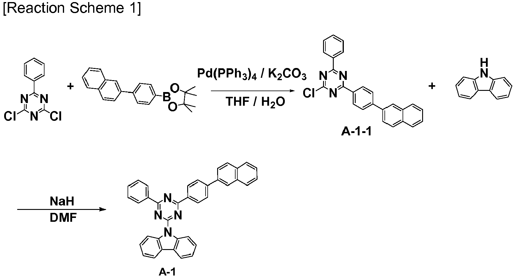
- 2,4-Dichloro-6-phenyl-1,3,5-triazine (21.0 g, 93.12 mmol), 4,4,5,5-tetramethyl-2-(4-naphthalen-2-yl-phenyl)-[1,3,2]dioxaborolane (20.5 g, 62.08 mmol), tetrakis(triphenylphosphine)palladium (2.1 g, 1.86 mmol), and potassium carbonate (17.1 g, 124.16 mmol) were put in a round-bottomed flask and dissolved in 200 mL of tetrahydrofuran and 100 mL of distilled water and then, heated and refluxed under a nitrogen atmosphere. After 6 hours, the reaction solution was cooled down, and after removing an aqueous layer therefrom, an organic layer therein was dried under a reduced pressure. The obtained solid was washed with water and methanol and recrystallized with 400 mL of toluene to obtain 18.0 g (yield of 74%) of Intermediate A-1-1.
- Intermediate A-1-1 (22.5 g 57.2 mmol) and carbazole (7.9 g, 47.6 mmol) were dissolved in 200 mL of DMF, and NaH was added thereto. After stirred the mixture at room temperature for 4 hours, the reaction solution was added to 500 mL of water to form a precipitate. A solid formed therein was filtered and then, washed with water and methanol. The obtained solid was recrystallized in 500 mL of chlorobenzene to obtain 22.8 g (91%) of Compound A-1.
LC/MS calculated for: C37H24N4 Exact Mass: 524.20 found for 524.25 [M+H] -

- 15.0 g (61%) of Intermediate A-3-1 was synthesized according to the same method as the a) of Synthesis Example 1 except that 2-biphenyl-4-yl-4,6-dichloro-[1,3,5]triazine (28.14 g, 93.15 mmol) and 4,4,5,5-tetramethyl-2-(4-naphthalen-1-yl-phenyl)-[1,3,2]dioxaborolane (20.5 g, 62.08 mmol) were used.
- 25.0 g (83%) of Compound A-3 was synthesized according the same method as the b) of Synthesis Example 1 except that Intermediate A-3-1 (26.9 g 57.19 mmol) and carbazole (9.5 g, 57.2 mmol) were used.
LC/MS calculated for: C43H28N4 Exact Mass: 600.23 found for 600.28 [M+H] -

- Intermediate A-1-1 (20.0 g, 50.78 mmol), 9-[4-(4,4,5,5-tetramethyl-[1,3,2]dioxaborolan-2-yl)-phenyl]-9H-carbazole (22.5 g, 60.93 mmol), and tetrakis(triphenylphosphine)palladium (1.7 g, 1.52 mmol), and potassium carbonate (14.0 g, 101.56 mmol) were dissolved in 300 mL of tetrahydrofuran and 150 mL of distilled water in a round-bottomed flask and then, heated and refluxed under a nitrogen atmosphere. After 12 hours, the reaction solution was cooled down, and after removing an aqueous layer therefrom, an organic layer therein was dried under a reduced pressure. The obtained solid was washed with water and methanol and then, recrystallized with 600 mL of monochlorobenzene to obtain 27.5 g (yield of 90%) of Compound A-17.
LC/MS calculated for: C43H28N4 Exact Mass: 600.23 found for 600.27 [M+H] -

- 13.9 g (91%) of Compound A-18 was synthesized according to the same method as Synthesis Example 3 except that Intermediate A-1-1 (10.0 g, 25.39 mmol) and 9-[3-(4,4,5,5-tetramethyl-[1,3,2]dioxaborolan-2-yl)-phenyl]-9H-carbazole (11.2 g, 30.47 mmol) were used.
LC/MS calculated for: C43H28N4 Exact Mass: 600.23 found for 600.27 [M+H] -

- 12.0 g (49%) of Intermediate A-19-1 were synthesized according to the same method as the a) of Synthesis Example 1 except that 2,4-dichloro-6-phenyl-1,3,5-triazine (21.1 g, 93.12 mmol) and 4,4,5,5-tetramethyl-2-(3-naphthalen-1-yl-phenyl)-[1,3,2]dioxaborolane (20.5 g, 62.08 mmol) were used.
- 13.9 g (91%) of Compound A-19 were synthesized according the same method as Synthesis Example 3 except that Intermediate A-19-1 (10.0 g, 25.39 mmol) and 9-[4-(4,4,5,5-tetramethyl-[1,3,2]dioxaborolan-2-yl)-phenyl]-9H-carbazole (11.2 g, 30.47 mmol) were used.
LC/MS calculated for: C43H28N4 Exact Mass: 600.23 found for 600.28 [M+H] -
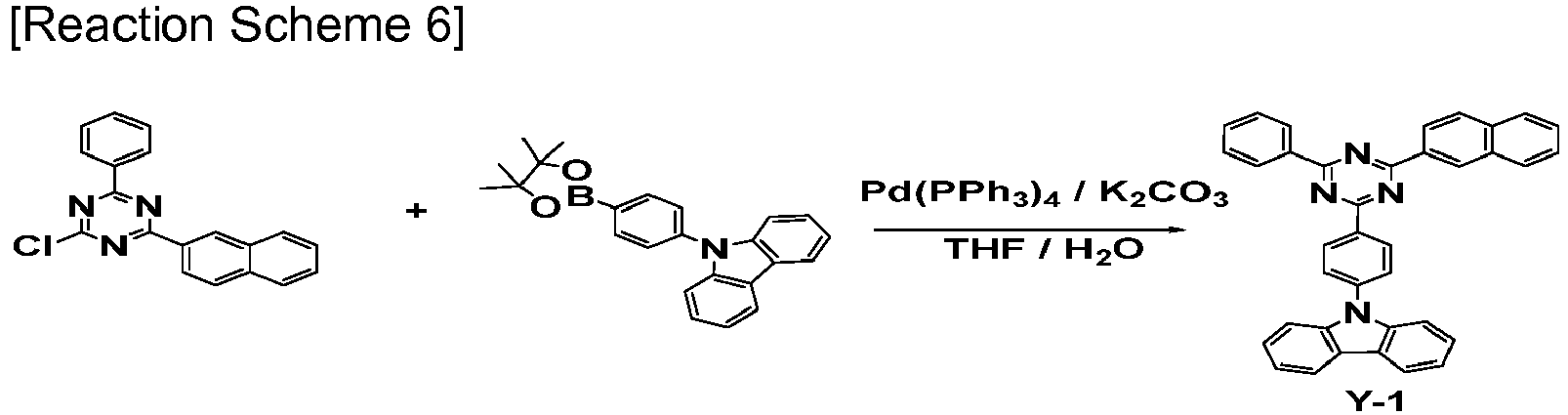
- 15.0 g (91%) of Compound Y-1 was synthesized according to the same method as Synthesis Example 3 except that an intermediate of 2-chloro-4-naphthalen-2-yl-6-phenyl-[1,3,5]triazine (10.0 g, 31.47 mmol) and 9-[4-(4,4,5,5-tetramethyl-[1,3,2]dioxaborolan-2-yl)-phenyl]-9H-carbazole (11.6 g, 31.47 mmol) were used.
LC/MS calculated for: C37H24N4 Exact Mass: 524.20 found for 524.27 [M+H] -


- 18.0 g (73%) of Compound Y-2 were synthesized according to the same method as Synthesis Example 3 except that 2-chloro-4-naphthalen-1-yl-6-phenyl-[1,3,5]triazine (15.0 g, 47.20 mmol) and 9-[4-(4,4,5,5-tetramethyl-[1,3,2]dioxaborolan-2-yl)-phenyl]-9H-carbazole (17.4 g, 47.20 mmol) were used.
LC/MS calculated for: C37H24N4 Exact Mass: 524.20 found for 524.25 [M+H] -

- 17.0 g (49%) of Intermediate Y-3-1 were synthesized according to the same method as the a) of Synthesis Example 1 except that an intermediate of 2,4-dichloro-6-phenyl-1,3,5-triazine (20.0 g, 88.47 mmol) and 4,4,5,5-tetramethyl-2-(4-naphthalen-1-yl-phenyl)-[1,3,2]dioxaborolane (27.76 g, 84.05 mmol) were used.
- 15.0 g (82%) of Intermediate Y-3 were synthesized according to the same method as Synthesis Example 3 except that Intermediate Y-3-1 (12.0 g, 30.47 mmol) and 9-[4-(4,4,5,5-tetramethyl-[1,3,2]dioxaborolan-2-yl)-phenyl]-9H-carbazole (13.5 g, 35.56 mmol) were used.
LC/MS calculated for: C43H28N4 Exact Mass: 600.23 found for 600.28 [M+H] -

- 12.0 g (75%) of Intermediate Y-4 were synthesized according to the same method as Synthesis Example 3 except that 2-biphenyl-4-yl-4-chloro-6-phenyl-[1,3,5]triazine (10.0 g, 29.09 mmol) and 9-[4-(4,4,5,5-tetramethyl-[1,3,2]dioxaborolan-2-yl)-phenyl]-9H-carbazole (12.9 g, 34.90 mmol) were used.
LC/MS calculated for: C39H26N4 Exact Mass: 550.22 found for 550.27 [M+H] -


- 10.0 g (66%) of Compound Y-5 were synthesized according to the same method as Synthesis Example 3 except that an intermediate of 4-chloro-6-(4-naphthalen-2-yl-phenyl)-2-phenyl-pyrimidine (10.0 g, 25.45 mmol) and 9-[4-(4,4,5,5-tetramethyl-[1,3,2]dioxaborolan-2-yl)-phenyl]-9H-carbazole (11.28 g, 30.54 mmol) were used.
LC/MS calculated for: C44H29N3 Exact Mass: 599.24 found for 599.29 [M+H] - A glass substrate coated with ITO (indium tin oxide) as a 1500 A-thick thin film was washed with distilled water. After washing with the distilled water, the glass substrate was ultrasonic wave-washed with a solvent such as isopropyl alcohol, acetone, methanol, and the like and dried and then, moved to a plasma cleaner, cleaned by using oxygen plasma for 10 minutes, and moved to a vacuum depositor. This obtained ITO transparent electrode was used as an anode, Compound A was vacuum-deposited on the ITO substrate to form a 700 A-thick hole injection layer, and Compound B was deposited to be 50 Å-thick on the hole injection layer, and then Compound C was deposited to be 700 A-thick to form a hole transport layer. On the hole transport layer, Compound C-1 was vacuum-deposited to be a 400 A-thick to form a hole transport auxiliary layer. On the hole transport auxiliary layer, 400 A-thick light emitting layer was formed by using Compound A-1 as a host and doping 2 wt% of [Ir(piq)2acac] as a dopant by a vacuum-deposition. Subsequently, on the light emitting layer, a 300 Å-thick electron transport layer was formed by simultaneously vacuum-depositing Compound D and Liq in a ratio of 1:1, and on the electron transport layer, Liq and Al were sequentially vacuum-deposited to be 15 Å-thick and 1200 Å-thick. An organic light emitting diode was thus manufactured.
- The organic light emitting diode had a five-layered organic thin layer, and specifically the following structure.
- ITO/Compound A (700 Å)/Compound B (50 Å)/Compound C (700 Å)/Compound C-1 (400 Å)/EML [Compound A-1: [Ir(piq)2acac] (2 wt%)] (400 Å)/Compound D : Liq (300 Å)/Liq (15 Å)/Al (1200 Å).
- Compound A: N4,N4'-diphenyl-N4,N4'-bis(9-phenyl-9H-carbazol-3-yl)biphenyl-4,4'-diamine
- Compound B: 1,4,5,8,9,11-hexaazatriphenylene-hexacarbonitrile (HAT-CN)
- Compound C: N-(biphenyl-4-yl)-9,9-dimethyl-N-(4-(9-phenyl-9H-carbazol-3-yl)phenyl)-9H-fluoren-2-amine
- Compound C-1: N,N-di([1,1'-biphenyl]-4-yl)-7,7-dimethyl-7H-fluoreno[4,3-b]benzofuran-10-amine
- Compound D: 8-(4-(4,6-di(naphthalen-2-yl)-1,3,5-triazin-2-yl)phenyl)quinoline
- Each organic light emitting diode was manufactured according to the same method as Example 1 except that the host compounds were changed as in Table 1.
- Each organic light emitting diode was manufactured according to the same method as Example 1 except that the host compounds were changed as in Table 1.
- Power efficiency of the organic light emitting diodes according to Examples 1 to 5 and Comparative Examples 1 to 5 was evaluated.
- Specific measurement methods are as follows, and the results are shown in Table 1.
- The obtained organic light emitting diodes were measured regarding a current value flowing in the unit device, while increasing the voltage from 0 V to 10 V using a current-voltage meter (Keithley 2400), and the measured current value was divided by area to provide the results.
- Luminance was measured by using a luminance meter (Minolta Cs-1000A), while the voltage of the organic light emitting diodes was increased from 0 V to 10 V.
- Power efficiency (cd/A) at the same current density (10 mA/cm2) were calculated by using the luminance, current density, and voltages (V) from the items (1) and (2).
- The results were obtained by measuring a time when current efficiency (cd/A) was decreased down to 90%, while luminance (cd/m2) was maintained to be 6000 cd/m2.
- A driving voltage of each diode was measured using a current-voltage meter (Keithley 2400) at 15 mA/cm2.
[Table 1] Host Color Power efficiency (cd/A) Driving voltage (V) Life-span T90 (h) Example 1 A-1 red 11.1 4.54 75 Example 2 A-3 red 12.0 4.45 70 Example 3 A-17 red 13.4 4.28 95 Example 4 A-18 red 13.8 4.15 80 Example 5 A-19 red 13.5 4.30 78 Comparative Example 1 Y-1 red 7.5 4.92 30 Comparative Example 2 Y-2 red 7.3 5.18 3 Comparative Example 3 Y-3 red 3.4 6.23 3 Comparative Example 4 Y-4 red 7.9 4.81 2 Comparative Example 5 Y-5 red 8.2 5.96 25 - Referring to Table 1, the organic light emitting diodes according to Examples 1 to 5 exhibited greatly improved driving voltages, efficiency, and life-span compared with the organic light emitting diodes according to Comparative Examples 1 to 5.
- While this invention has been described in connection with what is presently considered to be practical embodiments, it is to be understood that the invention is not limited to the disclosed embodiments, but, on the contrary, is intended to cover various modifications and equivalent arrangements included within the spirit and scope of the appended claims.
-
- 100, 200: organic light emitting diode
- 105: organic layer
- 110: cathode
- 120: anode
- 130: light emitting layer
- 140: hole auxiliary layer
Claims (10)
- A compound for an organic optoelectronic device represented by Chemical Formula 1:
 Ar1 is a substituted or unsubstituted C6 to C18 aryl group,L1 is a substituted or unsubstituted C6 to C20 arylene group, a substituted or unsubstituted C2 to C20 heteroarylene group, or a combination thereof, andL2 is a single bond or a substituted or unsubstituted phenylene group.
 - The compound for an organic optoelectronic device of claim 1, wherein L1 is a substituted or unsubstituted phenylene group or a substituted or unsubstituted biphenylene group.
- The compound for an organic optoelectronic device of claim 1 or 2, wherein L1 is one of linking groups of Group I:

- The compound for an organic optoelectronic device of any of the claims 1 to 3, wherein Ar1 is a substituted or unsubstituted phenyl group, a substituted or unsubstituted biphenyl group, or a substituted or unsubstituted terphenyl group.
- The compound for an organic optoelectronic device of any of the claims 1 to 4, wherein Ar1 is one of substituents of Group II:

- The compound for an organic optoelectronic device of any of the claims 1 to 5, which is one of compounds of Group A:


- An organic optoelectronic device, comprising
an anode and a cathode facing each other,
at least one organic layer disposed between the anode and the cathode,
wherein the organic layer comprises the compound for an organic optoelectronic device of any one of claim 1 to claim 6. - The organic optoelectronic device of claim 7, wherein
the organic layer comprises a light emitting layer, and
the light emitting layer comprises the compound for the organic optoelectronic device. - The organic optoelectronic device of claim 7 or 8, wherein the compound for the organic optoelectronic device is included as a phosphorescent host of the light emitting layer.
- A display device comprising the organic optoelectronic device of any of the claims 7 to 9.
Applications Claiming Priority (1)
| Application Number | Priority Date | Filing Date | Title |
|---|---|---|---|
| KR1020180149835A KR102213664B1 (en) | 2018-11-28 | 2018-11-28 | Compound for optoelectronic device and organic optoelectronic device and display device |
Publications (2)
| Publication Number | Publication Date |
|---|---|
| EP3660012A1 true EP3660012A1 (en) | 2020-06-03 |
| EP3660012B1 EP3660012B1 (en) | 2021-05-19 |
Family
ID=68731703
Family Applications (1)
| Application Number | Title | Priority Date | Filing Date |
|---|---|---|---|
| EP19211892.5A Active EP3660012B1 (en) | 2018-11-28 | 2019-11-27 | Compound for organic optoelectronic device and organic optoelectronic device and display device |
Country Status (6)
| Country | Link |
|---|---|
| US (1) | US11637247B2 (en) |
| EP (1) | EP3660012B1 (en) |
| JP (1) | JP6864063B2 (en) |
| KR (1) | KR102213664B1 (en) |
| CN (1) | CN111233838A (en) |
| TW (1) | TWI747087B (en) |
Families Citing this family (2)
| Publication number | Priority date | Publication date | Assignee | Title |
|---|---|---|---|---|
| KR102031300B1 (en) * | 2018-12-21 | 2019-10-11 | 삼성에스디아이 주식회사 | Compound for organic optoelectronic device, composition for organic optoelectronic device and organic optoelectronic device and display device |
| KR20260056722A (en) * | 2024-10-18 | 2026-04-27 | 삼성에스디아이 주식회사 | Organic optoelectronic device and display device |
Citations (7)
| Publication number | Priority date | Publication date | Assignee | Title |
|---|---|---|---|---|
| US5061569A (en) | 1990-07-26 | 1991-10-29 | Eastman Kodak Company | Electroluminescent device with organic electroluminescent medium |
| JPH059471A (en) | 1991-07-03 | 1993-01-19 | Mitsui Toatsu Chem Inc | Organic electroluminescent device |
| WO1995009147A1 (en) | 1993-09-29 | 1995-04-06 | Idemitsu Kosan Co., Ltd. | Organic electroluminescent element and arylenediamine derivative |
| JPH07126615A (en) | 1993-11-01 | 1995-05-16 | Matsushita Electric Ind Co Ltd | Electroluminescent device |
| JPH1095973A (en) | 1996-07-24 | 1998-04-14 | Mitsui Petrochem Ind Ltd | Luminescent compound for traveling control and traveling control method using the compound |
| WO2013073874A1 (en) * | 2011-11-18 | 2013-05-23 | Rohm And Haas Electronic Materials Korea Ltd. | Novel organic electroluminescent compounds and an organic electroluminescent device using the same |
| WO2014054912A1 (en) * | 2012-10-04 | 2014-04-10 | Rohm And Haas Electronic Materials Korea Ltd. | Organic electroluminescent compounds and organic electroluminescent device comprising the same |
Family Cites Families (30)
| Publication number | Priority date | Publication date | Assignee | Title |
|---|---|---|---|---|
| EP2169028B1 (en) | 2002-03-22 | 2018-11-21 | Idemitsu Kosan Co., Ltd. | Material for organic electroluminescent devices and organic electroluminescent devices made by using the same |
| WO2008117826A1 (en) | 2007-03-27 | 2008-10-02 | Nippon Steel Chemical Co., Ltd. | Compound for organic electroluminescent device and organic electroluminescent device |
| JP2010138121A (en) | 2008-12-12 | 2010-06-24 | Canon Inc | Triazine compound, and organic light emitting element employing the same |
| KR101288557B1 (en) | 2008-12-24 | 2013-07-22 | 제일모직주식회사 | Novel compound for organic photoelectric device and organic photoelectric device including the same |
| JP5167381B2 (en) | 2011-03-24 | 2013-03-21 | パナソニック株式会社 | Organic electroluminescence device |
| KR101813865B1 (en) | 2011-04-07 | 2018-01-02 | 미쯔비시 케미컬 주식회사 | Organic compound, charge transport material, composition containing said compound, organic electroluminescent element, display device, and lighting device |
| KR20120116282A (en) | 2011-04-12 | 2012-10-22 | 롬엔드하스전자재료코리아유한회사 | Novel organic electroluminescence compounds and organic electroluminescence device using the same |
| WO2013175747A1 (en) | 2012-05-22 | 2013-11-28 | 出光興産株式会社 | Organic electroluminescent element |
| CN103664894B (en) * | 2012-08-30 | 2016-12-28 | 昆山维信诺显示技术有限公司 | A kind of 6H naphtho-[2,1,8,7 klmn] a word used for translation derivant and application thereof |
| JP2014096417A (en) * | 2012-11-07 | 2014-05-22 | Idemitsu Kosan Co Ltd | Organic electroluminescent element and electronic device |
| JP5662991B2 (en) * | 2012-12-14 | 2015-02-04 | パナソニックIpマネジメント株式会社 | Organic electroluminescence device |
| WO2014122933A1 (en) | 2013-02-08 | 2014-08-14 | ソニー株式会社 | Organic electroluminescent element |
| KR102145885B1 (en) | 2013-06-05 | 2020-08-20 | 삼성디스플레이 주식회사 | Heterocyclic compound and organic light emitting device comprising same |
| KR102411748B1 (en) | 2014-03-17 | 2022-06-23 | 롬엔드하스전자재료코리아유한회사 | Electron Buffering Material and Organic Electroluminescent Device |
| KR101804630B1 (en) | 2014-09-05 | 2017-12-05 | 주식회사 엘지화학 | Multicyclic compound including nitrogen and organic electronic device using the same |
| KR101641781B1 (en) | 2014-09-12 | 2016-07-21 | 주식회사 엘지화학 | Organic light emitting device |
| KR101803599B1 (en) | 2014-09-12 | 2017-12-01 | 주식회사 엘지화학 | Organic light emitting diode |
| KR101709379B1 (en) | 2014-10-01 | 2017-02-23 | 주식회사 엘지화학 | Organic light emitting device |
| KR20160039492A (en) | 2014-10-01 | 2016-04-11 | 가톨릭대학교 산학협력단 | Compounds for organic optoelectronic device and organic optoelectronic device including the same |
| CN105646458A (en) | 2014-11-13 | 2016-06-08 | 上海和辉光电有限公司 | Compound and preparation method and application thereof |
| WO2016080749A1 (en) | 2014-11-18 | 2016-05-26 | Rohm And Haas Electronic Materials Korea Ltd. | A plurality of dopant materials and organic electroluminescent device comprising the same |
| CN107635978B (en) | 2016-01-26 | 2020-12-01 | 株式会社Lg化学 | Heterocyclic compound and organic light-emitting device comprising the same |
| KR102027030B1 (en) | 2016-05-27 | 2019-09-30 | 주식회사 엘지화학 | Organic light emitting device |
| KR20180063708A (en) | 2016-12-02 | 2018-06-12 | (주)피엔에이치테크 | An electroluminescent compound and an electroluminescent device comprising the same |
| JP7551273B2 (en) | 2018-01-11 | 2024-09-17 | 三星電子株式会社 | Compound, material for organic electroluminescence device, composition for organic electroluminescence device, and organic electroluminescence device |
| US11706977B2 (en) * | 2018-01-11 | 2023-07-18 | Samsung Electronics Co., Ltd. | Heterocyclic compound, composition including the same, and organic light-emitting device including the heterocyclic compound |
| US11077757B2 (en) * | 2018-05-03 | 2021-08-03 | Hyundai Motor Company | Vehicle and control method thereof |
| US11802124B2 (en) | 2018-07-09 | 2023-10-31 | Lg Chem, Ltd. | Compound and organic light emitting diode comprising same |
| KR102258085B1 (en) | 2018-10-04 | 2021-05-28 | 삼성에스디아이 주식회사 | Composition for organic optoelectronic device and organic optoelectronic device and display device |
| KR20200056811A (en) | 2018-11-15 | 2020-05-25 | 엘티소재주식회사 | Heterocyclic compound and organic light emitting device comprising the same |
-
2018
- 2018-11-28 KR KR1020180149835A patent/KR102213664B1/en active Active
-
2019
- 2019-11-25 US US16/693,959 patent/US11637247B2/en active Active
- 2019-11-27 CN CN201911179401.7A patent/CN111233838A/en active Pending
- 2019-11-27 EP EP19211892.5A patent/EP3660012B1/en active Active
- 2019-11-27 TW TW108143109A patent/TWI747087B/en active
- 2019-11-28 JP JP2019215421A patent/JP6864063B2/en active Active
Patent Citations (7)
| Publication number | Priority date | Publication date | Assignee | Title |
|---|---|---|---|---|
| US5061569A (en) | 1990-07-26 | 1991-10-29 | Eastman Kodak Company | Electroluminescent device with organic electroluminescent medium |
| JPH059471A (en) | 1991-07-03 | 1993-01-19 | Mitsui Toatsu Chem Inc | Organic electroluminescent device |
| WO1995009147A1 (en) | 1993-09-29 | 1995-04-06 | Idemitsu Kosan Co., Ltd. | Organic electroluminescent element and arylenediamine derivative |
| JPH07126615A (en) | 1993-11-01 | 1995-05-16 | Matsushita Electric Ind Co Ltd | Electroluminescent device |
| JPH1095973A (en) | 1996-07-24 | 1998-04-14 | Mitsui Petrochem Ind Ltd | Luminescent compound for traveling control and traveling control method using the compound |
| WO2013073874A1 (en) * | 2011-11-18 | 2013-05-23 | Rohm And Haas Electronic Materials Korea Ltd. | Novel organic electroluminescent compounds and an organic electroluminescent device using the same |
| WO2014054912A1 (en) * | 2012-10-04 | 2014-04-10 | Rohm And Haas Electronic Materials Korea Ltd. | Organic electroluminescent compounds and organic electroluminescent device comprising the same |
Also Published As
| Publication number | Publication date |
|---|---|
| CN111233838A (en) | 2020-06-05 |
| KR20200063737A (en) | 2020-06-05 |
| JP2020088398A (en) | 2020-06-04 |
| TW202020114A (en) | 2020-06-01 |
| US11637247B2 (en) | 2023-04-25 |
| US20200168813A1 (en) | 2020-05-28 |
| EP3660012B1 (en) | 2021-05-19 |
| KR102213664B1 (en) | 2021-02-05 |
| TWI747087B (en) | 2021-11-21 |
| JP6864063B2 (en) | 2021-04-21 |
| KR102213664B9 (en) | 2022-03-23 |
Similar Documents
| Publication | Publication Date | Title |
|---|---|---|
| EP3901148B1 (en) | Compound for organic optoelectronic element, composition for organic optoelectronic element and organic optoelectronic element and display device | |
| EP3575296B1 (en) | Triazine compound, composition and organic optoelectronic device and display device | |
| EP3664172B1 (en) | Compound for organic optoelectronic diode, organic optoelectronic diode, and display device | |
| EP3643762B1 (en) | Organic optoelectronic element and display device | |
| EP3553050B1 (en) | Composition and organic optoelectronic device and display device | |
| EP3480278B1 (en) | Compound for organic optoelectronic device, composition for organic optoelectronic device, organic optoelectronic device and display apparatus | |
| EP3486299B1 (en) | Compound for organic optoelectronic device, composition for organic optoelectronic device, organic optoelectronic device, and display device | |
| EP3657559A1 (en) | Organic optoelectronic diode and display device | |
| EP4027403A1 (en) | Organic alloy for organic optoelectronic device, organic optoelectronic device, and display device | |
| KR20200072211A (en) | Compound for optoelectronic device and organic optoelectronic device and display device | |
| US11362281B2 (en) | Compound for organic optoelectronic diode, composition for organic optoelectronic diode, organic optoelectronic diode, and display apparatus | |
| EP3992190A1 (en) | Compound for organic optoelectronic diode, composition for organic optoelectronic diode, organic optoelectronic diode, and display device | |
| CN110003127B (en) | Composition, organic optoelectronic device and display device | |
| EP4273148A1 (en) | Compound for organic optoelectronic element, composition for organic optoelectronic element, organic optoelectronic element, and display device | |
| EP3660012B1 (en) | Compound for organic optoelectronic device and organic optoelectronic device and display device | |
| US11690288B2 (en) | Composition for organic optoelectronic diode, organic optoelectronic diode, and display device | |
| KR20210039831A (en) | Compound for organic optoelectronic device, organic optoelectronic device and display device | |
| US12213378B2 (en) | Compound for organic optoelectronic device, organic optoelectronic device, and display device | |
| CN113943307B (en) | Compound for organic photoelectric device, composition for organic photoelectric device, and display device | |
| KR102430048B1 (en) | Compound for optoelectronic device and organic optoelectronic device and display device | |
| CN112368853B (en) | Compound for organic optoelectronic element, composition for organic optoelectronic element, organic optoelectronic element and display device | |
| KR102448567B1 (en) | Compounds for organic optoelectronic devices, organic optoelectronic devices and display devices |
Legal Events
| Date | Code | Title | Description |
|---|---|---|---|
| PUAI | Public reference made under article 153(3) epc to a published international application that has entered the european phase |
Free format text: ORIGINAL CODE: 0009012 |
|
| STAA | Information on the status of an ep patent application or granted ep patent |
Free format text: STATUS: REQUEST FOR EXAMINATION WAS MADE |
|
| 17P | Request for examination filed |
Effective date: 20191127 |
|
| AK | Designated contracting states |
Kind code of ref document: A1 Designated state(s): AL AT BE BG CH CY CZ DE DK EE ES FI FR GB GR HR HU IE IS IT LI LT LU LV MC MK MT NL NO PL PT RO RS SE SI SK SM TR |
|
| AX | Request for extension of the european patent |
Extension state: BA ME |
|
| RBV | Designated contracting states (corrected) |
Designated state(s): AL AT BE BG CH CY CZ DE DK EE ES FI FR GB GR HR HU IE IS IT LI LT LU LV MC MK MT NL NO PL PT RO RS SE SI SK SM TR |
|
| GRAP | Despatch of communication of intention to grant a patent |
Free format text: ORIGINAL CODE: EPIDOSNIGR1 |
|
| STAA | Information on the status of an ep patent application or granted ep patent |
Free format text: STATUS: GRANT OF PATENT IS INTENDED |
|
| INTG | Intention to grant announced |
Effective date: 20201223 |
|
| GRAS | Grant fee paid |
Free format text: ORIGINAL CODE: EPIDOSNIGR3 |
|
| GRAA | (expected) grant |
Free format text: ORIGINAL CODE: 0009210 |
|
| STAA | Information on the status of an ep patent application or granted ep patent |
Free format text: STATUS: THE PATENT HAS BEEN GRANTED |
|
| AK | Designated contracting states |
Kind code of ref document: B1 Designated state(s): AL AT BE BG CH CY CZ DE DK EE ES FI FR GB GR HR HU IE IS IT LI LT LU LV MC MK MT NL NO PL PT RO RS SE SI SK SM TR |
|
| REG | Reference to a national code |
Ref country code: GB Ref legal event code: FG4D |
|
| REG | Reference to a national code |
Ref country code: CH Ref legal event code: EP |
|
| REG | Reference to a national code |
Ref country code: DE Ref legal event code: R096 Ref document number: 602019004737 Country of ref document: DE |
|
| REG | Reference to a national code |
Ref country code: AT Ref legal event code: REF Ref document number: 1393855 Country of ref document: AT Kind code of ref document: T Effective date: 20210615 |
|
| REG | Reference to a national code |
Ref country code: IE Ref legal event code: FG4D |
|
| REG | Reference to a national code |
Ref country code: LT Ref legal event code: MG9D |
|
| REG | Reference to a national code |
Ref country code: AT Ref legal event code: MK05 Ref document number: 1393855 Country of ref document: AT Kind code of ref document: T Effective date: 20210519 |
|
| REG | Reference to a national code |
Ref country code: NL Ref legal event code: MP Effective date: 20210519 |
|
| PG25 | Lapsed in a contracting state [announced via postgrant information from national office to epo] |
Ref country code: BG Free format text: LAPSE BECAUSE OF FAILURE TO SUBMIT A TRANSLATION OF THE DESCRIPTION OR TO PAY THE FEE WITHIN THE PRESCRIBED TIME-LIMIT Effective date: 20210819 Ref country code: AT Free format text: LAPSE BECAUSE OF FAILURE TO SUBMIT A TRANSLATION OF THE DESCRIPTION OR TO PAY THE FEE WITHIN THE PRESCRIBED TIME-LIMIT Effective date: 20210519 Ref country code: HR Free format text: LAPSE BECAUSE OF FAILURE TO SUBMIT A TRANSLATION OF THE DESCRIPTION OR TO PAY THE FEE WITHIN THE PRESCRIBED TIME-LIMIT Effective date: 20210519 Ref country code: LT Free format text: LAPSE BECAUSE OF FAILURE TO SUBMIT A TRANSLATION OF THE DESCRIPTION OR TO PAY THE FEE WITHIN THE PRESCRIBED TIME-LIMIT Effective date: 20210519 Ref country code: FI Free format text: LAPSE BECAUSE OF FAILURE TO SUBMIT A TRANSLATION OF THE DESCRIPTION OR TO PAY THE FEE WITHIN THE PRESCRIBED TIME-LIMIT Effective date: 20210519 |
|
| PG25 | Lapsed in a contracting state [announced via postgrant information from national office to epo] |
Ref country code: GR Free format text: LAPSE BECAUSE OF FAILURE TO SUBMIT A TRANSLATION OF THE DESCRIPTION OR TO PAY THE FEE WITHIN THE PRESCRIBED TIME-LIMIT Effective date: 20210820 Ref country code: IS Free format text: LAPSE BECAUSE OF FAILURE TO SUBMIT A TRANSLATION OF THE DESCRIPTION OR TO PAY THE FEE WITHIN THE PRESCRIBED TIME-LIMIT Effective date: 20210919 Ref country code: LV Free format text: LAPSE BECAUSE OF FAILURE TO SUBMIT A TRANSLATION OF THE DESCRIPTION OR TO PAY THE FEE WITHIN THE PRESCRIBED TIME-LIMIT Effective date: 20210519 Ref country code: PL Free format text: LAPSE BECAUSE OF FAILURE TO SUBMIT A TRANSLATION OF THE DESCRIPTION OR TO PAY THE FEE WITHIN THE PRESCRIBED TIME-LIMIT Effective date: 20210519 Ref country code: NO Free format text: LAPSE BECAUSE OF FAILURE TO SUBMIT A TRANSLATION OF THE DESCRIPTION OR TO PAY THE FEE WITHIN THE PRESCRIBED TIME-LIMIT Effective date: 20210819 Ref country code: RS Free format text: LAPSE BECAUSE OF FAILURE TO SUBMIT A TRANSLATION OF THE DESCRIPTION OR TO PAY THE FEE WITHIN THE PRESCRIBED TIME-LIMIT Effective date: 20210519 Ref country code: SE Free format text: LAPSE BECAUSE OF FAILURE TO SUBMIT A TRANSLATION OF THE DESCRIPTION OR TO PAY THE FEE WITHIN THE PRESCRIBED TIME-LIMIT Effective date: 20210519 Ref country code: PT Free format text: LAPSE BECAUSE OF FAILURE TO SUBMIT A TRANSLATION OF THE DESCRIPTION OR TO PAY THE FEE WITHIN THE PRESCRIBED TIME-LIMIT Effective date: 20210920 |
|
| PG25 | Lapsed in a contracting state [announced via postgrant information from national office to epo] |
Ref country code: NL Free format text: LAPSE BECAUSE OF FAILURE TO SUBMIT A TRANSLATION OF THE DESCRIPTION OR TO PAY THE FEE WITHIN THE PRESCRIBED TIME-LIMIT Effective date: 20210519 |
|
| PG25 | Lapsed in a contracting state [announced via postgrant information from national office to epo] |
Ref country code: SK Free format text: LAPSE BECAUSE OF FAILURE TO SUBMIT A TRANSLATION OF THE DESCRIPTION OR TO PAY THE FEE WITHIN THE PRESCRIBED TIME-LIMIT Effective date: 20210519 Ref country code: ES Free format text: LAPSE BECAUSE OF FAILURE TO SUBMIT A TRANSLATION OF THE DESCRIPTION OR TO PAY THE FEE WITHIN THE PRESCRIBED TIME-LIMIT Effective date: 20210519 Ref country code: EE Free format text: LAPSE BECAUSE OF FAILURE TO SUBMIT A TRANSLATION OF THE DESCRIPTION OR TO PAY THE FEE WITHIN THE PRESCRIBED TIME-LIMIT Effective date: 20210519 Ref country code: DK Free format text: LAPSE BECAUSE OF FAILURE TO SUBMIT A TRANSLATION OF THE DESCRIPTION OR TO PAY THE FEE WITHIN THE PRESCRIBED TIME-LIMIT Effective date: 20210519 Ref country code: CZ Free format text: LAPSE BECAUSE OF FAILURE TO SUBMIT A TRANSLATION OF THE DESCRIPTION OR TO PAY THE FEE WITHIN THE PRESCRIBED TIME-LIMIT Effective date: 20210519 Ref country code: RO Free format text: LAPSE BECAUSE OF FAILURE TO SUBMIT A TRANSLATION OF THE DESCRIPTION OR TO PAY THE FEE WITHIN THE PRESCRIBED TIME-LIMIT Effective date: 20210519 Ref country code: SM Free format text: LAPSE BECAUSE OF FAILURE TO SUBMIT A TRANSLATION OF THE DESCRIPTION OR TO PAY THE FEE WITHIN THE PRESCRIBED TIME-LIMIT Effective date: 20210519 |
|
| REG | Reference to a national code |
Ref country code: DE Ref legal event code: R097 Ref document number: 602019004737 Country of ref document: DE |
|
| PLBE | No opposition filed within time limit |
Free format text: ORIGINAL CODE: 0009261 |
|
| STAA | Information on the status of an ep patent application or granted ep patent |
Free format text: STATUS: NO OPPOSITION FILED WITHIN TIME LIMIT |
|
| 26N | No opposition filed |
Effective date: 20220222 |
|
| PG25 | Lapsed in a contracting state [announced via postgrant information from national office to epo] |
Ref country code: IS Free format text: LAPSE BECAUSE OF FAILURE TO SUBMIT A TRANSLATION OF THE DESCRIPTION OR TO PAY THE FEE WITHIN THE PRESCRIBED TIME-LIMIT Effective date: 20210919 Ref country code: AL Free format text: LAPSE BECAUSE OF FAILURE TO SUBMIT A TRANSLATION OF THE DESCRIPTION OR TO PAY THE FEE WITHIN THE PRESCRIBED TIME-LIMIT Effective date: 20210519 |
|
| PG25 | Lapsed in a contracting state [announced via postgrant information from national office to epo] |
Ref country code: MC Free format text: LAPSE BECAUSE OF FAILURE TO SUBMIT A TRANSLATION OF THE DESCRIPTION OR TO PAY THE FEE WITHIN THE PRESCRIBED TIME-LIMIT Effective date: 20210519 |
|
| PG25 | Lapsed in a contracting state [announced via postgrant information from national office to epo] |
Ref country code: LU Free format text: LAPSE BECAUSE OF NON-PAYMENT OF DUE FEES Effective date: 20211127 Ref country code: IT Free format text: LAPSE BECAUSE OF FAILURE TO SUBMIT A TRANSLATION OF THE DESCRIPTION OR TO PAY THE FEE WITHIN THE PRESCRIBED TIME-LIMIT Effective date: 20210519 Ref country code: BE Free format text: LAPSE BECAUSE OF NON-PAYMENT OF DUE FEES Effective date: 20211130 |
|
| REG | Reference to a national code |
Ref country code: BE Ref legal event code: MM Effective date: 20211130 |
|
| PG25 | Lapsed in a contracting state [announced via postgrant information from national office to epo] |
Ref country code: IE Free format text: LAPSE BECAUSE OF NON-PAYMENT OF DUE FEES Effective date: 20211127 |
|
| PG25 | Lapsed in a contracting state [announced via postgrant information from national office to epo] |
Ref country code: FR Free format text: LAPSE BECAUSE OF NON-PAYMENT OF DUE FEES Effective date: 20211130 |
|
| PG25 | Lapsed in a contracting state [announced via postgrant information from national office to epo] |
Ref country code: CY Free format text: LAPSE BECAUSE OF FAILURE TO SUBMIT A TRANSLATION OF THE DESCRIPTION OR TO PAY THE FEE WITHIN THE PRESCRIBED TIME-LIMIT Effective date: 20210519 |
|
| REG | Reference to a national code |
Ref country code: CH Ref legal event code: PL |
|
| P01 | Opt-out of the competence of the unified patent court (upc) registered |
Effective date: 20230528 |
|
| PG25 | Lapsed in a contracting state [announced via postgrant information from national office to epo] |
Ref country code: LI Free format text: LAPSE BECAUSE OF NON-PAYMENT OF DUE FEES Effective date: 20221130 Ref country code: HU Free format text: LAPSE BECAUSE OF FAILURE TO SUBMIT A TRANSLATION OF THE DESCRIPTION OR TO PAY THE FEE WITHIN THE PRESCRIBED TIME-LIMIT; INVALID AB INITIO Effective date: 20191127 Ref country code: CH Free format text: LAPSE BECAUSE OF NON-PAYMENT OF DUE FEES Effective date: 20221130 |
|
| PG25 | Lapsed in a contracting state [announced via postgrant information from national office to epo] |
Ref country code: MK Free format text: LAPSE BECAUSE OF FAILURE TO SUBMIT A TRANSLATION OF THE DESCRIPTION OR TO PAY THE FEE WITHIN THE PRESCRIBED TIME-LIMIT Effective date: 20210519 |
|
| GBPC | Gb: european patent ceased through non-payment of renewal fee |
Effective date: 20231127 |
|
| PG25 | Lapsed in a contracting state [announced via postgrant information from national office to epo] |
Ref country code: MT Free format text: LAPSE BECAUSE OF FAILURE TO SUBMIT A TRANSLATION OF THE DESCRIPTION OR TO PAY THE FEE WITHIN THE PRESCRIBED TIME-LIMIT Effective date: 20210519 |
|
| PG25 | Lapsed in a contracting state [announced via postgrant information from national office to epo] |
Ref country code: GB Free format text: LAPSE BECAUSE OF NON-PAYMENT OF DUE FEES Effective date: 20231127 |
|
| PG25 | Lapsed in a contracting state [announced via postgrant information from national office to epo] |
Ref country code: GB Free format text: LAPSE BECAUSE OF NON-PAYMENT OF DUE FEES Effective date: 20231127 |
|
| PG25 | Lapsed in a contracting state [announced via postgrant information from national office to epo] |
Ref country code: TR Free format text: LAPSE BECAUSE OF FAILURE TO SUBMIT A TRANSLATION OF THE DESCRIPTION OR TO PAY THE FEE WITHIN THE PRESCRIBED TIME-LIMIT Effective date: 20210519 |
|
| PGFP | Annual fee paid to national office [announced via postgrant information from national office to epo] |
Ref country code: DE Payment date: 20251104 Year of fee payment: 7 |