EP3657680A1 - Touch button structure and electrical device - Google Patents
Touch button structure and electrical device Download PDFInfo
- Publication number
- EP3657680A1 EP3657680A1 EP18908364.5A EP18908364A EP3657680A1 EP 3657680 A1 EP3657680 A1 EP 3657680A1 EP 18908364 A EP18908364 A EP 18908364A EP 3657680 A1 EP3657680 A1 EP 3657680A1
- Authority
- EP
- European Patent Office
- Prior art keywords
- touch
- conductive
- touch panel
- key structure
- touch key
- Prior art date
- Legal status (The legal status is an assumption and is not a legal conclusion. Google has not performed a legal analysis and makes no representation as to the accuracy of the status listed.)
- Granted
Links
Images








Classifications
-
- H—ELECTRICITY
- H03—ELECTRONIC CIRCUITRY
- H03K—PULSE TECHNIQUE
- H03K17/00—Electronic switching or gating, i.e. not by contact-making and –breaking
- H03K17/94—Electronic switching or gating, i.e. not by contact-making and –breaking characterised by the way in which the control signals are generated
- H03K17/96—Touch switches
- H03K17/962—Capacitive touch switches
- H03K17/9622—Capacitive touch switches using a plurality of detectors, e.g. keyboard
-
- H—ELECTRICITY
- H03—ELECTRONIC CIRCUITRY
- H03K—PULSE TECHNIQUE
- H03K17/00—Electronic switching or gating, i.e. not by contact-making and –breaking
- H03K17/94—Electronic switching or gating, i.e. not by contact-making and –breaking characterised by the way in which the control signals are generated
- H03K17/96—Touch switches
- H03K17/962—Capacitive touch switches
-
- G—PHYSICS
- G06—COMPUTING OR CALCULATING; COUNTING
- G06F—ELECTRIC DIGITAL DATA PROCESSING
- G06F3/00—Input arrangements for transferring data to be processed into a form capable of being handled by the computer; Output arrangements for transferring data from processing unit to output unit, e.g. interface arrangements
- G06F3/01—Input arrangements or combined input and output arrangements for interaction between user and computer
- G06F3/03—Arrangements for converting the position or the displacement of a member into a coded form
- G06F3/041—Digitisers, e.g. for touch screens or touch pads, characterised by the transducing means
- G06F3/044—Digitisers, e.g. for touch screens or touch pads, characterised by the transducing means by capacitive means
-
- H—ELECTRICITY
- H01—ELECTRIC ELEMENTS
- H01H—ELECTRIC SWITCHES; RELAYS; SELECTORS; EMERGENCY PROTECTIVE DEVICES
- H01H13/00—Switches having rectilinearly-movable operating part or parts adapted for pushing or pulling in one direction only, e.g. push-button switch
- H01H13/02—Details
- H01H13/023—Light-emitting indicators
-
- H—ELECTRICITY
- H03—ELECTRONIC CIRCUITRY
- H03K—PULSE TECHNIQUE
- H03K2217/00—Indexing scheme related to electronic switching or gating, i.e. not by contact-making or -breaking covered by H03K17/00
- H03K2217/94—Indexing scheme related to electronic switching or gating, i.e. not by contact-making or -breaking covered by H03K17/00 characterised by the way in which the control signal is generated
- H03K2217/96—Touch switches
- H03K2217/96015—Constructional details for touch switches
- H03K2217/96023—Details of electro-mechanic connections between different elements, e.g.: sensing plate and integrated circuit containing electronics
-
- H—ELECTRICITY
- H03—ELECTRONIC CIRCUITRY
- H03K—PULSE TECHNIQUE
- H03K2217/00—Indexing scheme related to electronic switching or gating, i.e. not by contact-making or -breaking covered by H03K17/00
- H03K2217/94—Indexing scheme related to electronic switching or gating, i.e. not by contact-making or -breaking covered by H03K17/00 characterised by the way in which the control signal is generated
- H03K2217/96—Touch switches
- H03K2217/9607—Capacitive touch switches
- H03K2217/960755—Constructional details of capacitive touch and proximity switches
Definitions
- the present disclosure relates to the technical field of touch control technology, and in particular, to a touch key structure and an electrical appliance.
- the touch key configured to replace the traditional mechanical key.
- the touch key has following advantages over the traditional mechanical key:
- Capacitive touch-sensing key as the most common touch key, is actually just a small piece of "metal electrode" on the PCB, which forms a sensing capacitor with the surrounding "ground signal".
- metal electrode On the PCB, which forms a sensing capacitor with the surrounding "ground signal".
- the electric field would be interfered, causing a corresponding change in capacitance.
- an insulating cover layer such as glass layer should be placed on the sensing electrode due to safety factor and aesthetics factor etc., and the human finger is coupled with the metal sensing sheet through the cover to make the induced capacitance change (usually several pF).
- FIGS. 1 to 3 shows a capacitive touch sensing key 100' having a capacitive sensor constructed by using the spring
- the capacitive touch sensing key 100' includes a touch panel 1', a PCB board 2' and a key support 3'.
- a space is formed between the touch panel 1' and the PCB board 2' to accommodate components such as the wire plug (not labeled), the digital tube (not labeled), and a spring 4', etc.
- PCB board 2' is soldered with the spring 4'.
- the spring 4' abuts between the touch panel 1' and the PCB board 2' through its both ends.
- the spring 4' is prone to skew as it is compressed and tightened by the panel, which is prone to skew. If it is subjected to large amplitude vibration or impact during use, the spring 4' is easily detached from the installation position, causing the touch function to fail.
- the main objective of the present disclosure is to provide a touch key structure and an electrical appliance, which aims to improve a simple and reliable touch key structure to solve the problems of the complex structure and poor stability of the existing capacitive touch-sensing key structure.
- a touch key structure including:
- the present disclosure further provides an electrical appliance including a touch key structure, the touch key structure including:
- a sensing electrode is provided on the circuit board, and a conductive medium is provided between a key area of the touch panel and the sensing electrode.
- the finger and the sensing electrode form a capacitance.
- the capacitance is increased because the conductive medium is provided, and can be sensitively sensed when a finger approaches or touches the key area. Therefore, in the present disclosure, the sensing electrode and the conductive medium are easy to be installed and have good stability after installation, thereby making the touch key structure simple and reliable.
- Table 1 Label Name Label Name 100' Capacitive touch-sensing key 3' Key support 1' Touch panel 4' Spring 2' PCB board
- Table 2 Label Name Label Name 100 Touch key structure 3 Conductive medium 1 Touch panel 3a Conductive layer 1a Pillar 3b Conductive body 1b Cylindrical body 4 Support 2 Circuit board 41 Mounting hole 21 Sensing electrode 42 Convex part
- the descriptions, such as the "first”, the “second” in the embodiment of present disclosure can only be used for describing the aim of description, and cannot be understood as indicating or suggesting relative importance or impliedly indicating the number of the indicated technical character. Therefore, the character indicated by the "first”, the “second” can express or impliedly include at least one character.
- the technical solution of each embodiment can be combined with each other, however the technical solution must base on that the ordinary skill in that art can realize the technical solution, when the combination of the technical solutions is contradictory or cannot be realized, it should consider that the combination of the technical solutions does not exist, and is beyond the protection scope of the present disclosure.
- the present disclosure provides a touch key structure and an electrical appliance having the touch key structure.
- the electric appliance may be a cooking appliance, such as a rice cooker, an induction cooker, a cooking machine, a soymilk maker, or the like, and may also be other electric appliance such as an air conditioner, which is not limited in this application. All electrical appliances provided with the touch key structure are within the protection scope of the present disclosure, and the touch key structure provided in the present disclosure will be specifically described below with reference to the drawings.
- FIGS. 4 to 8 are a touch key structure according to a first embodiment of the present disclosure
- FIGS. 9 to 16 are a touch key structure according to a second embodiment of the present disclosure
- FIGS. 17 to 23 are a touch key structure according to a third embodiment of the present disclosure
- FIGS. 24 to 33 are a touch key structure according to a forth embodiment of the present disclosure
- FIGS. 34 to 35 are a touch key structure according to a fifth embodiment of the present disclosure.
- the touch key structure 100 includes a touch panel 1, a circuit board 2, and a conductive medium 3.
- the front side of the touch panel 1 has a key area for a user to touch (touch or approach) (in most cases, the key area forms a key identification, and the key identification may be a silk screen structure, or a bright area where LED light sees through the key area, etc.).
- the circuit board 2 is provided behind the touch panel 1, and a sensing electrode 21 is provided on the circuit board 2 corresponding to the key area.
- the conductive medium 3 is provided between the key area and the sensing electrode 21.
- the sensing electrode 21 and the finger constitute a capacitor, which is referred to as a "touch capacitor", and the formation process is not described in detail.
- the conductive medium 3 is equivalent to adding a conductor between two electrodes of the touch capacitor, so that the touch capacitor becomes larger and it is easier to detect a finger. Therefore, in the present disclosure, the sensing electrode 21 and the conductive medium 3 are easy to be installed and have good stability after installation, thereby making the touch key structure 100 simple and reliable in structure.
- the number and shape of the key area are not limited, and a plurality of the key areas set at a single point can be provided, or the key area can also be a sliding touch area set continuously.
- a plurality of the key areas, a plurality of the sensing electrodes 21 and a plurality of conductive media 3 are provided, and the key areas are in a one-to-one correspondence with the sensing electrodes 21 and the conductive media 3, and the specific number varies depending on the actual number of key areas.
- the relationship between the sensing electrode 21, the conductive medium 3, and the key area is not necessarily one-to-one correspondence, and one sensing electrode 21 may correspond to multiple key areas.
- the fingers are located in different key areas, and the capacitance between the finger and the sensing electrode 21 changes to identify different keys.
- the material, structure, and shape of the conductive medium 3 are also not limited, depending on actual needs or the difficulty, cost, and so on of production and manufacturing.
- the conductive medium 3 may be made of a metal material, and the metal material has a high conductivity, which makes the touch capacitor have a larger capacitance.
- the conductive medium 3 may be a conductive body 3b or a conductive layer 3a.
- the conductive body 3b may be a metal conductive body 3b or a non-metal + metal mixed conductive body 3b.
- the conductive layer 3a may be provided through physical means or chemical plating.
- the conductive layer 3a may be provided through water plating, evaporation, sputtering, electrophoresis, vacuum plating, spray coating, coating, chemical plating, etc.
- the physical means includes one of spray coating, brush coating, vacuum plating, and the like. Among them, spray coating, brush coating or vacuum plating can be selected, which is low cost and easy to implement.
- the touch key structure 100 further includes a support 4, which is provided between the circuit board 2 and the touch panel 1.
- the conductive medium 3 is provided on the support 4, and specifically, the support 4 is a key support, and the circuit board 2 is provided with an LED lamp.
- the key support is also provided with a cylindrical structure for accommodating LED indicators. The cylindrical structure isolates the LED lights to avoid mutual influence of light between the LED lights, so that the LED lights form an indication identification on the touch panel 1.
- the support should be made of an insulating material.
- the support 4 may be made of an insulating material with a material resistivity of 10 10 ⁇ .cm to 10 14 ⁇ .cm.
- the conductive medium may be made of a material with a resistivity of less than 10 10 ⁇ .cm, and may be made of a material with a resistivity of less than 10 4 ⁇ .cm. The lower the resistivity, the better the conductivity, and the higher the sensitivity of the touch key structure 100.
- the conductive medium 3 is a conductive body 3b provided on the support 4.
- the conductive body 3b can be provided in various shapes and sizes.
- the conductive body 3b has sufficient conductive medium, so that the touch key structure 100 has better touch sensitivity.
- the conductive body 3b may be a metal conductive body 3b.
- the conductive body 3b may be reliably installed on the support 4, the conductive body 3b and the support 4 are relatively easy to be fixed, and the connection relationship between the conductive body 3b and the support 4 is not limited.
- the conductive body 3b is integrally connected with the support 4 through a secondary molding method.
- the support 4 is injection-molded first, and then the molded support 4 is inserted into a mold to form the conductive body 3b, so that the conductive body 3b is integrally connected with the support 4.
- the conductive body 3b will not be loose due to other mechanical connection methods, which will affect the touch sensitivity of the touch key structure 100, thereby making the touch key structure 100 stable and reliable.
- the conductive body 3b is installed in the mounting hole 41 and at least one end (both ends in the present embodiment) of the conductive body 3b is exposed to the mounting hole 41, such that the conductive body 3b has a sufficient length.
- the distance between the sensing electrode 2 and the touch panel 1 is relatively short, thereby making the touch key structure 100 more sensitive.
- the conductive medium 3 is a conductive layer 3a provided on the support 4. Compared with providing the conductive body 3b on the support, it is easier to provide the conductive layer 3a on the support 4, and there is no problem of assembling and mounting between the conductive body 3b and the support 4.
- the conductive layer 3a may be formed on the support 4 through a physical means such as spray coating, brush coating, or vacuum plating or chemical plating.
- the support 4 is provided with a mounting hole 41, and the conductive layer 3a is provided in the mounting hole 41. Since the mounting hole 41 can form a sealing space by itself or by means of an external fixture, the conductive layer 3a may be provided on the inner wall of the mounting hole 41 through vacuum plating. Of course, it is obviously not limited to this, and chemical plating may also be used.
- the mounting hole 41 may be a blind hole or a through hole. Please refer to FIG. 14 to FIG. 15 , the mounting hole 41 is a through hole to avoid having an insulator between the key area and the sensing electrode 21, thereby affecting the size of the sensing capacitor and affecting the sensitivity of the touch key structure 100. Referring to FIG. 16 , the mounting hole 41 is a blind hole. That is, only one end of the mounting hole 41 is opened. For this reason, when the conductive layer 3a is provided, vacuum plating may be preferentially used.
- the support 4 in order to make the conductive medium 3 have a sufficiently large size in the inner-outer direction, the support 4 includes a convex part 42 protruded towards at least one side, and the mounting hole 41 is penetrated through the convex part 42.
- the support 4 includes two convex parts 42 protruded towards both sides, the mounting hole 41 is penetrated through the two convex parts 42, such that the distance between the conductive medium 3 and the sensing electrode 21 and the distance between the conductive medium 3 and the key area are both small, so that the touch capacitance is sufficiently large and the sensing sensitivity is higher.
- the outer surfaces of the convex parts 42 are all provided with the conductive layer 3a, and enough conductive medium 3 can be arranged, so that the touch capacitance is sufficiently large and the sensing sensitivity is higher.
- the conductive medium 3 is provided on a rear side of the touch panel 1. In this way, the structure of the support 4 can be omitted compared to the first and second embodiments. Obviously, the design is not limited to this.
- the conductive medium 3 may be embedded in the touch panel 1.
- the touch panel 1 is provided in multiple layers, and the conductive medium 3 is an intermediate layer provided on the touch panel 1, or a cavity may be formed inside the touch panel 1.
- the surface of the touch panel 1 is provided with an entrance communicating with the cavity, and the conductive medium 3 is provided in the cavity from the entrance.
- the conductive medium 3 is a conductive body 3b provided on the rear side of the touch panel 1.
- the conductive body 3b may be fixed to the rear side of the touch panel 1 through, for example, screws, buckles, adhesives, and the like.
- the conductive body 3b is integrally connected with the touch panel 1 through secondary molding. Specially, first, the touch panel 1 is injection-molded, and then the formed touch panel 1 is embedded in a mold to form the conductive body 3b, such that the touch panel 1 is integrally connected with the conductive body 3b.
- the conductive body 3b will not be loosened due to other mechanical connection methods, which will affect the touch sensitivity of the touch key structure 100.
- the conductive body 3b is in a cylindrical shape with openings at both ends, and one end of the conductive body 3b is connected to the touch panel 1, to facilitate the connection between the conductive body 3b and the touch panel 1.
- the conductive body 3b is in a cylindrical shape with an open end and a closed end, and the closed end of the conductive body 3b is connected to the touch panel 1, such that there is a sufficient area between the conductive body 3b and the sensing electrode 21, which makes the touch capacitance larger.
- FIG. 21 the conductive body 3b is in a cylindrical shape with openings at both ends, and one end of the conductive body 3b is connected to the touch panel 1, to facilitate the connection between the conductive body 3b and the touch panel 1.
- the conductive body 3b is in a cylindrical shape with an open end and a closed end, and the closed end of the conductive body 3b is connected to the touch panel 1, such that there is a sufficient area between the conductive body 3b and the sensing electrode 21, which makes the touch capacitance larger.
- the conductive body 3b is a solid conductive body 3b structure, and one end of the conductive body 3b is connected to the touch panel 1, such that the size of the conductive body 3b is larger, which makes the touch capacitance larger, thereby making the touch key structure 100 more sensitive.
- the conductive medium 3 is a conductive layer 3a provided on the rear side of the touch panel 1.
- the conductive layer 3a is easier to combine with the touch panel 1 than the conductive body 3b.
- the conductive layer 3a may be directly formed on the rear side of the touch panel 1 through physical means (coating, brushing, and vacuum plating) or chemical plating.
- the areas where the conductive layer 3a is provided are all protruding towards the touch electrode, and the specific shape of protruding structure is not limited. Referring to FIGS. 29 to 31 , a cylindrical body 1b with an opening towards the circuit board 2 is protruded on the rear side of the touch panel 1, and the conductive layer 3b is provided on an inner side, an outer side, and/or a rear end of the cylindrical body 1b. As shown in FIG.
- the conductive layer 3b is provided on the outer side of the cylindrical body 1b, such that the conductive layer 3a can be provided on the cylindrical body 1b through spraying or brushing, which is convenient for installation.
- the conductive layer 3b is provided on the inner side, the outer side, and the rear end surface of the cylindrical body 1, such that the layout area of the conductive layer 3a is large, which makes the touch capacitance larger.
- the conductive layer 3b is provided on the inner side of the cylindrical body 1, and the conductive layer 3a can be formed through vacuum plating or chemical plating. Referring to FIGS.
- a pillar 1a is protruded on the rear side of the touch panel 1, and the conductive layer 3a is provided on an outer side and/or a rear end surface of the pillar 1a.
- the conductive layer 3a is only provided on the outer side of the pillar 1a.
- the conductive layer 3a is provided on both the outer side and the end surface of the pillar 1a, and a sufficient number of the conductive media 3 can be provided.
- a distance between the conductive medium 3 and the sensing electrode 21 is d1
- a distance between the conductive medium 3 and the touch panel 1 is d2.
- the smaller d1 and d2 indicate that the distance between the conductive medium 3 and the sensing electrode 21 and the key area is sufficiently small, so that the touch capacitance is small and the sensitivity is high.
- a sum of d1 and d2 is greater than or equal to 0 and less than or equal to 2mm.
- a periphery of the area where the conductive medium 3 is laid out is exceeding the sensing electrode 21, such that the conductive medium 3 can completely cover the edge of the sensing electrode 21.
- an exceeding size cannot be too large, if it is too large, the distance between adjacent conductive media 3 is too small. Therefore, in the present embodiment, a periphery of the conductive medium 3 is exceeding the sensing electrode 21, and an exceeding size is H, and H is less than or equal to 3mm.
- the conductive medium 3 is a conductive layer 3a formed through spraying, and a thickness of the conductive layer 3a is D.
- D a thickness of the conductive layer 3a
- D is greater than or equal to 10 ⁇ m and less than or equal to 25 ⁇ m.
- a size of the conductive medium is K in a front-rear direction, and K is less than 15mm.
- the conductive medium 3 may be a discontinuous structure.
- the conductive medium 3 includes a plurality of sections arranged on the front-rear direction, and may also be a continuous structure.
- the touch capacitance is larger than the discontinuous structure.
- each of the conductive media 3 is continuously disposed.
- the conductive medium 3 is a conductive layer 3a, and the conductive medium 3 is made of the material selected from one of nickel powder, aluminum powder, silver powder, and silver copper powder. These metals have good stability and excellent electrical conductivity.
- a support 4 is provided between the touch panel 1 and the circuit board 2, a mounting hole 41 is defined in the support 4, and the conductive medium 3 is a conductive layer 3a provided on an inner wall of the mounting hole 41.
- the conductive medium is a conductive paint, and preferably, the resistance value of the conductive paint is controlled between 0.2 ⁇ and 0.6 ⁇ . Therefore, the touch key structure 100 has proper sensitivity.
- the conductive medium 3 is a conductive layer 3a, and the conductive medium 3 is made of the material selected from one of nickel powder, aluminum powder, silver powder, and silver copper powder. These metals have good stability and excellent electrical conductivity. And/or,
- the support 4 is made of an insulating material suitable for injection molding and selected from one of PP, ABS, PA, PMMA, PC, PC/ABS, and bakelite.
Landscapes
- Engineering & Computer Science (AREA)
- General Engineering & Computer Science (AREA)
- Theoretical Computer Science (AREA)
- Human Computer Interaction (AREA)
- Physics & Mathematics (AREA)
- General Physics & Mathematics (AREA)
- Switches That Are Operated By Magnetic Or Electric Fields (AREA)
- Input From Keyboards Or The Like (AREA)
Abstract
Description
- The present disclosure relates to the technical field of touch control technology, and in particular, to a touch key structure and an electrical appliance.
- Electronics are equipped with the touch key configured to replace the traditional mechanical key. The touch key has following advantages over the traditional mechanical key:
- 1. Without any movable mechanical parts, the touch key will not wear out and has an infinite life, which reduces the subsequent maintenance costs.
- 2. The sensing part of the touch key can be placed behind any insulating layer (such as, glass layer or plastic layer or ceramic layer, etc.), so the sensing part may be easily made into a sealed keyboard, thereby protecting it from moisture and water.
- 3. The panel pattern, the size and shape of the touch key can be arbitrarily designed, and characters, trademarks, perspective windows, etc., can be arbitrarily matched with each other. So the touch key has advantages that the metal panels and the mechanical panels do not have, such as, beautiful and fashionable appearance, no fading, no deformation, and good durability. As such the touch key can replace the existing ordinary panels (including metal keyboard, membrane keyboard, conductive plastic keyboard) due to its reliability and arbitrary aesthetic design.
- Capacitive touch-sensing key, as the most common touch key, is actually just a small piece of "metal electrode" on the PCB, which forms a sensing capacitor with the surrounding "ground signal". When a finger is close to the area above the electrode, the electric field would be interfered, causing a corresponding change in capacitance. Based on the change in capacitance, whether a human body approaches or touches the touch key can be detected. For the current capacitive touch-sensing key, an insulating cover layer such as glass layer should be placed on the sensing electrode due to safety factor and aesthetics factor etc., and the human finger is coupled with the metal sensing sheet through the cover to make the induced capacitance change (usually several pF). However, in some applications, since wire plug, digital tube, capacitor and LED are on the circuit board, the circuit board cannot be directly mounted under the cove. So that some transfer methods are needed. The most common method is to build a capacitive sensor using a spring. For example,
FIGS. 1 to 3 shows a capacitive touch sensing key 100' having a capacitive sensor constructed by using the spring, the capacitive touch sensing key 100' includes a touch panel 1', a PCB board 2' and a key support 3'. A space is formed between the touch panel 1' and the PCB board 2' to accommodate components such as the wire plug (not labeled), the digital tube (not labeled), and a spring 4', etc.. PCB board 2' is soldered with the spring 4'. The spring 4' abuts between the touch panel 1' and the PCB board 2' through its both ends. - However, there are many disadvantages to the spring 4', which is taken as a sensing electrode, resisting between the PCB 2' and the touch panel 1':
First, because each key must be equipped with one spring 4', the cost is increased. - Besides, the processes of mounting and soldering the spring 4' on the PCB board 2' are both relatively complicated. The pin of the touch spring 4' should be inserted into the through hole of the PCB board 2', then the spring 4' is soldered with the PCB board 2' through wave soldering. A lot of labor and fixtures are required, and the process is prone to appear problems such as loosening, skewing, displacement, poor welding, etc., which increases the cost of the process and the difficulty of quality assurance.
- In addition, during the complete assembly of the product, the spring 4' is prone to skew as it is compressed and tightened by the panel, which is prone to skew. If it is subjected to large amplitude vibration or impact during use, the spring 4' is easily detached from the installation position, causing the touch function to fail.
- In view of this, it is necessary to improve the existing capacitive touch-sensing key to provide a reliable capacitive touch-sensing key further with an easy installation advantage.
- The main objective of the present disclosure is to provide a touch key structure and an electrical appliance, which aims to improve a simple and reliable touch key structure to solve the problems of the complex structure and poor stability of the existing capacitive touch-sensing key structure.
- In order to achieve the above objective, the present disclosure provides a touch key structure, including:
- a touch panel, wherein a front side of the touch panel has a key area for a user to touch;
- a circuit board provided behind the touch panel, wherein the circuit board is provided with a sensing electrode corresponding to the key area; and
- a conductive medium provided between the key area and the sensing electrode.
- The present disclosure further provides an electrical appliance including a touch key structure, the touch key structure including:
- a touch panel, wherein a front side of the touch panel has a key area for a user to touch;
- a circuit board provided behind the touch panel, wherein the circuit board is provided with a sensing electrode corresponding to the key area; and
- a conductive medium provided between the key area and the sensing electrode.
- In the technical solutions of the present disclosure, a sensing electrode is provided on the circuit board, and a conductive medium is provided between a key area of the touch panel and the sensing electrode. When a user's finger touches or approaches the key area, the finger and the sensing electrode form a capacitance. The capacitance is increased because the conductive medium is provided, and can be sensitively sensed when a finger approaches or touches the key area. Therefore, in the present disclosure, the sensing electrode and the conductive medium are easy to be installed and have good stability after installation, thereby making the touch key structure simple and reliable.
- In order to more clearly illustrate the embodiments of the present disclosure or the technical solutions in the related art, the drawings used in the embodiments or the related art will be briefly described below. Obviously, the drawings in the following description are only some embodiments of the present disclosure. It will be apparent to those skilled in the art that other figures can be obtained from the structures illustrated in the drawings without the inventive effort.
-
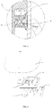
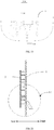
FIG. 1 is a schematic exploded perspective view of a capacitive touch-sensing key in the related art; -
FIG. 2 is a schematic cross-sectional view of the capacitive touch-sensing key inFIG. 1 ; -
FIG. 3 is an enlarged view of portion A' inFIG. 2 ; -
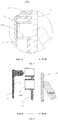
FIG. 4 is a schematic structural perspective view of a touch key structure according to a first embodiment of the present disclosure; -
FIG. 5 is a schematic structural plan view inFIG. 4 ; -
FIG. 6 is a schematic cross-sectional view taken along line L1-L1 inFIG. 4 ; -
FIG. 7 is an enlarged view of portion A1 inFIG. 6 ; -
FIG. 8 is a partial exploded schematic view inFIG. 6 ; -
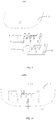
FIG. 9 is a schematic structural perspective view of a touch key structure according to a second embodiment of the present disclosure; -
FIG. 10 is a schematic structural plan view inFIG. 9 ; -
FIG. 11 is a schematic cross-sectional view taken along line L2-L2 inFIG. 10 ; -
FIG. 12 is an enlarged view of portion A2 inFIG. 11 ; -
FIG. 13 is a partial exploded schematic view inFIG. 11 ; -
FIG. 14 is a partial schematic structural view of the support and the conductive layer inFIG. 11 according to a first embodiment; -
FIG. 15 is a partial schematic structural view of the support and the conductive layer inFIG. 11 according to a second embodiment; -
FIG. 16 is a partial schematic structural view of the support and the conductive layer inFIG. 11 according to a third embodiment; -
FIG. 17 is a schematic structural perspective view of a touch key structure according to a third embodiment of the present disclosure; -
FIG. 18 is a schematic structural plan view inFIG. 17 ; -
FIG. 19 is a schematic cross-sectional view taken along line L3-L3 inFIG. 18 ; -
FIG. 20 is an enlarged view of portion A3 inFIG. 19 ; -
FIG. 21 is a partial schematic structural view of the touch panel and the conductive body inFIG. 18 according to a first embodiment; -
FIG. 22 is a partial schematic structural view of the touch panel and the conductive body inFIG. 18 according to a second embodiment; -
FIG. 23 is a partial schematic structural view of the touch panel and the conductive body inFIG. 18 according to a third embodiment; -
FIG. 24 is a schematic structural perspective view of a touch key structure according to a forth embodiment of the present disclosure; -
FIG. 25 is a schematic structural plan view inFIG. 24 ; -
FIG. 26 is a schematic cross-sectional view taken along line L4-L4 inFIG. 25 ; -
FIG. 27 is an enlarged view of portion A4 inFIG. 26 ; -
FIG. 28 is a partial exploded schematic view inFIG. 26 ; -
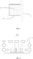
FIG. 29 is a partial schematic structural view of the touch panel and the conductive layer inFIG. 26 according to a first embodiment; -
FIG. 30 is a partial schematic structural view of the touch panel and the conductive layer inFIG. 26 according to a second embodiment; -
FIG. 31 is a partial schematic structural view of the touch panel and the conductive layer inFIG. 26 according to a third embodiment; -
FIG. 32 is a partial schematic structural view of the touch panel and the conductive layer inFIG. 26 according to a forth embodiment; -
FIG. 33 is a partial schematic structural view of the touch panel and the conductive layer inFIG. 26 according to a fifth embodiment; -
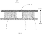
FIG. 34 is a schematic structural perspective view of a touch key structure according to a fifth embodiment of the present disclosure; and -
FIG. 35 is a schematic cross-sectional view inFIG. 34 . - Description of reference numerals in the related art:
Table 1 Label Name Label Name 100' Capacitive touch-sensing key 3' Key support 1' Touch panel 4' Spring 2' PCB board - Description of reference numerals in the present disclosure:
Table 2 Label Name Label Name 100 Touch key structure 3 Conductive medium 1 Touch panel 3a Conductive layer 1a Pillar 3b Conductive body 1b Cylindrical body 4 Support 2 Circuit board 41 Mounting hole 21 Sensing electrode 42 Convex part - The realization of the objective, functional characteristics, advantages of the present disclosure are further described with reference to the accompanying drawings.
- The technical solutions of the embodiments of the present disclosure will be clearly and completely described in the following with reference to the accompanying drawings. It is obvious that the embodiments to be described are only a part rather than all of the embodiments of the present disclosure. All other embodiments obtained by persons skilled in the art based on the embodiments of the present disclosure without creative efforts shall fall within the protection scope of the present disclosure.
- It is to be understood that, all of the directional instructions in the embodiments of the present disclosure (such as up, down, left, right, front, rear...) can only be used for explaining relative position relations, moving condition of the elements under a special form (referring to figures), and so on, if the special form changes, the directional instructions changes accordingly.
- In addition, the descriptions, such as the "first", the "second" in the embodiment of present disclosure, can only be used for describing the aim of description, and cannot be understood as indicating or suggesting relative importance or impliedly indicating the number of the indicated technical character. Therefore, the character indicated by the "first", the "second" can express or impliedly include at least one character. Besides, the technical solution of each embodiment can be combined with each other, however the technical solution must base on that the ordinary skill in that art can realize the technical solution, when the combination of the technical solutions is contradictory or cannot be realized, it should consider that the combination of the technical solutions does not exist, and is beyond the protection scope of the present disclosure.
- The present disclosure provides a touch key structure and an electrical appliance having the touch key structure. The electric appliance may be a cooking appliance, such as a rice cooker, an induction cooker, a cooking machine, a soymilk maker, or the like, and may also be other electric appliance such as an air conditioner, which is not limited in this application. All electrical appliances provided with the touch key structure are within the protection scope of the present disclosure, and the touch key structure provided in the present disclosure will be specifically described below with reference to the drawings.
FIGS. 4 to 8 are a touch key structure according to a first embodiment of the present disclosure;FIGS. 9 to 16 are a touch key structure according to a second embodiment of the present disclosure;FIGS. 17 to 23 are a touch key structure according to a third embodiment of the present disclosure;FIGS. 24 to 33 are a touch key structure according to a forth embodiment of the present disclosure; andFIGS. 34 to 35 are a touch key structure according to a fifth embodiment of the present disclosure. - In the embodiment of the present disclosure, referring to
FIGS. 4 to 8 , the touchkey structure 100 includes atouch panel 1, acircuit board 2, and aconductive medium 3. The front side of thetouch panel 1 has a key area for a user to touch (touch or approach) (in most cases, the key area forms a key identification, and the key identification may be a silk screen structure, or a bright area where LED light sees through the key area, etc.). Thecircuit board 2 is provided behind thetouch panel 1, and asensing electrode 21 is provided on thecircuit board 2 corresponding to the key area. Theconductive medium 3 is provided between the key area and thesensing electrode 21. - During a touch operation, a user's finger approaches or touches the key area, the
sensing electrode 21 and the finger constitute a capacitor, which is referred to as a "touch capacitor", and the formation process is not described in detail. Theconductive medium 3 is equivalent to adding a conductor between two electrodes of the touch capacitor, so that the touch capacitor becomes larger and it is easier to detect a finger. Therefore, in the present disclosure, thesensing electrode 21 and theconductive medium 3 are easy to be installed and have good stability after installation, thereby making the touchkey structure 100 simple and reliable in structure. - The number and shape of the key area are not limited, and a plurality of the key areas set at a single point can be provided, or the key area can also be a sliding touch area set continuously. In the embodiment of the present disclosure, a plurality of the key areas, a plurality of the
sensing electrodes 21 and a plurality ofconductive media 3 are provided, and the key areas are in a one-to-one correspondence with thesensing electrodes 21 and theconductive media 3, and the specific number varies depending on the actual number of key areas. Besides, the relationship between the sensingelectrode 21, theconductive medium 3, and the key area is not necessarily one-to-one correspondence, and onesensing electrode 21 may correspond to multiple key areas. The fingers are located in different key areas, and the capacitance between the finger and thesensing electrode 21 changes to identify different keys. - The material, structure, and shape of the
conductive medium 3 are also not limited, depending on actual needs or the difficulty, cost, and so on of production and manufacturing. Theconductive medium 3 may be made of a metal material, and the metal material has a high conductivity, which makes the touch capacitor have a larger capacitance. Theconductive medium 3 may be aconductive body 3b or aconductive layer 3a. Theconductive body 3b may be a metalconductive body 3b or a non-metal + metal mixedconductive body 3b. Alternatively, theconductive layer 3a may be provided through physical means or chemical plating. For example, theconductive layer 3a may be provided through water plating, evaporation, sputtering, electrophoresis, vacuum plating, spray coating, coating, chemical plating, etc. The physical means includes one of spray coating, brush coating, vacuum plating, and the like. Among them, spray coating, brush coating or vacuum plating can be selected, which is low cost and easy to implement. - The
conductive medium 3 is provided in a manner that is not limited, and may be provided on the touch panel or on a mounting structure between thetouch panel 1 and thecircuit board 2. The following describes it in combination with specific embodiments:
Referring toFIGS. 4 to 8 andFIGS. 9 to 16 , in the first embodiment and second embodiment of the present disclosure, the touchkey structure 100 further includes asupport 4, which is provided between thecircuit board 2 and thetouch panel 1. Theconductive medium 3 is provided on thesupport 4, and specifically, thesupport 4 is a key support, and thecircuit board 2 is provided with an LED lamp. The key support is also provided with a cylindrical structure for accommodating LED indicators. The cylindrical structure isolates the LED lights to avoid mutual influence of light between the LED lights, so that the LED lights form an indication identification on thetouch panel 1. - Obviously, the support should be made of an insulating material. For example, the
support 4 may be made of an insulating material with a material resistivity of 1010Ω.cm to 1014Ω.cm. The conductive medium may be made of a material with a resistivity of less than 1010Ω.cm, and may be made of a material with a resistivity of less than 104Ω.cm. The lower the resistivity, the better the conductivity, and the higher the sensitivity of the touchkey structure 100. - Referring to
FIGS. 4 to 8 , in the first embodiment of the present disclosure, theconductive medium 3 is aconductive body 3b provided on thesupport 4. Theconductive body 3b can be provided in various shapes and sizes. Theconductive body 3b has sufficient conductive medium, so that the touchkey structure 100 has better touch sensitivity. Theconductive body 3b may be a metalconductive body 3b. Theconductive body 3b may be reliably installed on thesupport 4, theconductive body 3b and thesupport 4 are relatively easy to be fixed, and the connection relationship between theconductive body 3b and thesupport 4 is not limited. In the present embodiment, theconductive body 3b is integrally connected with thesupport 4 through a secondary molding method. Specially, thesupport 4 is injection-molded first, and then the moldedsupport 4 is inserted into a mold to form theconductive body 3b, so that theconductive body 3b is integrally connected with thesupport 4. Theconductive body 3b will not be loose due to other mechanical connection methods, which will affect the touch sensitivity of the touchkey structure 100, thereby making the touchkey structure 100 stable and reliable. - Further, in the first embodiment of the present disclosure, referring to
FIG. 8 , theconductive body 3b is installed in the mountinghole 41 and at least one end (both ends in the present embodiment) of theconductive body 3b is exposed to the mountinghole 41, such that theconductive body 3b has a sufficient length. The distance between thesensing electrode 2 and thetouch panel 1 is relatively short, thereby making the touchkey structure 100 more sensitive. - Referring to
FIGS. 9 to 16 , in the second embodiment of the present disclosure, theconductive medium 3 is aconductive layer 3a provided on thesupport 4. Compared with providing theconductive body 3b on the support, it is easier to provide theconductive layer 3a on thesupport 4, and there is no problem of assembling and mounting between theconductive body 3b and thesupport 4. Theconductive layer 3a may be formed on thesupport 4 through a physical means such as spray coating, brush coating, or vacuum plating or chemical plating. - Specially, referring to
FIGS. 11 to 16 , in the present embodiment, thesupport 4 is provided with a mountinghole 41, and theconductive layer 3a is provided in the mountinghole 41. Since the mountinghole 41 can form a sealing space by itself or by means of an external fixture, theconductive layer 3a may be provided on the inner wall of the mountinghole 41 through vacuum plating. Of course, it is obviously not limited to this, and chemical plating may also be used. - The mounting
hole 41 may be a blind hole or a through hole. Please refer toFIG. 14 to FIG. 15 , the mountinghole 41 is a through hole to avoid having an insulator between the key area and thesensing electrode 21, thereby affecting the size of the sensing capacitor and affecting the sensitivity of the touchkey structure 100. Referring toFIG. 16 , the mountinghole 41 is a blind hole. That is, only one end of the mountinghole 41 is opened. For this reason, when theconductive layer 3a is provided, vacuum plating may be preferentially used. - Besides, in the present embodiment, in order to make the
conductive medium 3 have a sufficiently large size in the inner-outer direction, thesupport 4 includes aconvex part 42 protruded towards at least one side, and the mountinghole 41 is penetrated through theconvex part 42. Specially, in the present embodiment, thesupport 4 includes twoconvex parts 42 protruded towards both sides, the mountinghole 41 is penetrated through the twoconvex parts 42, such that the distance between theconductive medium 3 and thesensing electrode 21 and the distance between theconductive medium 3 and the key area are both small, so that the touch capacitance is sufficiently large and the sensing sensitivity is higher. - Further, in the present embodiment, referring to
FIG. 15 , the outer surfaces of theconvex parts 42 are all provided with theconductive layer 3a, and enough conductive medium 3 can be arranged, so that the touch capacitance is sufficiently large and the sensing sensitivity is higher. - Referring to
FIGS. 17 to 23 andFIGS. 24 to 33 , in the third and fourth embodiments of the touchkey structure 100 provided in the present disclosure, theconductive medium 3 is provided on a rear side of thetouch panel 1. In this way, the structure of thesupport 4 can be omitted compared to the first and second embodiments. Obviously, the design is not limited to this. Theconductive medium 3 may be embedded in thetouch panel 1. For example, thetouch panel 1 is provided in multiple layers, and theconductive medium 3 is an intermediate layer provided on thetouch panel 1, or a cavity may be formed inside thetouch panel 1. The surface of thetouch panel 1 is provided with an entrance communicating with the cavity, and theconductive medium 3 is provided in the cavity from the entrance. - Referring to
FIGS. 17 to 23 , according to a third embodiment of the present disclosure, theconductive medium 3 is aconductive body 3b provided on the rear side of thetouch panel 1. Theconductive body 3b may be fixed to the rear side of thetouch panel 1 through, for example, screws, buckles, adhesives, and the like. In the present embodiment, theconductive body 3b is integrally connected with thetouch panel 1 through secondary molding. Specially, first, thetouch panel 1 is injection-molded, and then the formedtouch panel 1 is embedded in a mold to form theconductive body 3b, such that thetouch panel 1 is integrally connected with theconductive body 3b. Theconductive body 3b will not be loosened due to other mechanical connection methods, which will affect the touch sensitivity of the touchkey structure 100. - The specific structure or shape of the
conductive body 3b is not limited. For example, referring toFIG. 21 , theconductive body 3b is in a cylindrical shape with openings at both ends, and one end of theconductive body 3b is connected to thetouch panel 1, to facilitate the connection between theconductive body 3b and thetouch panel 1. Alternatively, referring toFIG. 22 , theconductive body 3b is in a cylindrical shape with an open end and a closed end, and the closed end of theconductive body 3b is connected to thetouch panel 1, such that there is a sufficient area between theconductive body 3b and thesensing electrode 21, which makes the touch capacitance larger. Further, referring toFIG. 23 , theconductive body 3b is a solidconductive body 3b structure, and one end of theconductive body 3b is connected to thetouch panel 1, such that the size of theconductive body 3b is larger, which makes the touch capacitance larger, thereby making the touchkey structure 100 more sensitive. - Referring to
FIGS. 24 to 33 , according to a fourth embodiment of the present disclosure, theconductive medium 3 is aconductive layer 3a provided on the rear side of thetouch panel 1. Theconductive layer 3a is easier to combine with thetouch panel 1 than theconductive body 3b. Theconductive layer 3a may be directly formed on the rear side of thetouch panel 1 through physical means (coating, brushing, and vacuum plating) or chemical plating. - Besides, in order to make the
conductive medium 3 have a sufficient size in the inner and outer directions, and the distance between theconductive medium 3 and thesensing electrode 21 is small, so that the sensing sensitivity of the touchkey structure 100 is high. In the present embodiment, the areas where theconductive layer 3a is provided are all protruding towards the touch electrode, and the specific shape of protruding structure is not limited. Referring toFIGS. 29 to 31 , acylindrical body 1b with an opening towards thecircuit board 2 is protruded on the rear side of thetouch panel 1, and theconductive layer 3b is provided on an inner side, an outer side, and/or a rear end of thecylindrical body 1b. As shown inFIG. 29 , theconductive layer 3b is provided on the outer side of thecylindrical body 1b, such that theconductive layer 3a can be provided on thecylindrical body 1b through spraying or brushing, which is convenient for installation. As shown inFIG. 30 , theconductive layer 3b is provided on the inner side, the outer side, and the rear end surface of thecylindrical body 1, such that the layout area of theconductive layer 3a is large, which makes the touch capacitance larger. As shown inFIG. 31 , theconductive layer 3b is provided on the inner side of thecylindrical body 1, and theconductive layer 3a can be formed through vacuum plating or chemical plating. Referring toFIGS. 32 and33 , a pillar 1a is protruded on the rear side of thetouch panel 1, and theconductive layer 3a is provided on an outer side and/or a rear end surface of the pillar 1a. As shown inFIG. 32 , theconductive layer 3a is only provided on the outer side of the pillar 1a. As shown inFIG. 33 , theconductive layer 3a is provided on both the outer side and the end surface of the pillar 1a, and a sufficient number of theconductive media 3 can be provided. - Referring to
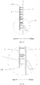
FIG. 34 andFIG. 35 , according to a fifth embodiment of the present disclosure, a distance between theconductive medium 3 and thesensing electrode 21 is d1, and a distance between theconductive medium 3 and thetouch panel 1 is d2. Theoretically, the smaller d1 and d2 indicate that the distance between theconductive medium 3 and thesensing electrode 21 and the key area is sufficiently small, so that the touch capacitance is small and the sensitivity is high. Thus, in the present embodiment, a sum of d1 and d2 is greater than or equal to 0 and less than or equal to 2mm. - A periphery of the area where the
conductive medium 3 is laid out is exceeding thesensing electrode 21, such that theconductive medium 3 can completely cover the edge of thesensing electrode 21. Obviously, an exceeding size cannot be too large, if it is too large, the distance between adjacentconductive media 3 is too small. Therefore, in the present embodiment, a periphery of theconductive medium 3 is exceeding thesensing electrode 21, and an exceeding size is H, and H is less than or equal to 3mm. - The
conductive medium 3 is aconductive layer 3a formed through spraying, and a thickness of theconductive layer 3a is D. Theoretically, the larger D is, the better, but the size of D is also limited by the process. In the present embodiment, D is greater than or equal to 10µm and less than or equal to 25µm. - In the present embodiment, limited by the distance between the
touch panel 1 and thecircuit board 2, a size of the conductive medium is K in a front-rear direction, and K is less than 15mm. - The
conductive medium 3 may be a discontinuous structure. For example, theconductive medium 3 includes a plurality of sections arranged on the front-rear direction, and may also be a continuous structure. When theconductive medium 3 is the continuous structure, the touch capacitance is larger than the discontinuous structure. In the present embodiment, each of theconductive media 3 is continuously disposed. - The
conductive medium 3 is aconductive layer 3a, and theconductive medium 3 is made of the material selected from one of nickel powder, aluminum powder, silver powder, and silver copper powder. These metals have good stability and excellent electrical conductivity. - In the present embodiment, a
support 4 is provided between thetouch panel 1 and thecircuit board 2, a mountinghole 41 is defined in thesupport 4, and theconductive medium 3 is aconductive layer 3a provided on an inner wall of the mountinghole 41. In the present embodiment, the conductive medium is a conductive paint, and preferably, the resistance value of the conductive paint is controlled between 0.2Ω and 0.6Ω. Therefore, the touchkey structure 100 has proper sensitivity. - The
conductive medium 3 is aconductive layer 3a, and theconductive medium 3 is made of the material selected from one of nickel powder, aluminum powder, silver powder, and silver copper powder. These metals have good stability and excellent electrical conductivity. And/or,
Thesupport 4 is made of an insulating material suitable for injection molding and selected from one of PP, ABS, PA, PMMA, PC, PC/ABS, and bakelite. - The above are only preferred embodiments of the present disclosure, and thus do not limit the scope of the present disclosure. In addition, in the case of no contradiction, the embodiments can be combined with each other. Under the concept of the present disclosure, the equivalent structural transformations made by the present specification and the drawings are directly or indirectly applied to other related technical fields, and are included in the scope of the present disclosure.
Claims (20)
- A touch key structure, comprising:a touch panel, wherein a front side of the touch panel has a key area for a user to touch;a circuit board provided behind the touch panel, wherein the circuit board is provided with a sensing electrode corresponding to the key area; anda conductive medium provided between the key area and the sensing electrode.
- The touch key structure of claim 1,
wherein a plurality of the key areas, a plurality of the sensing electrodes, and a plurality of the conductive media are provided, and the key areas are in a one-to-one correspondence with the sensing electrodes and the conductive media. - The touch key structure of claim 1,
wherein the conductive medium is a conductive body or a conductive layer, and
wherein the conductive layer is formed through a physical means or a chemical plating means. - The touch key structure of claim 1, further comprising:a support provided between the circuit board and the touch panel,wherein the conductive medium is provided on the support.
- The touch key structure of claim 4,
wherein the conductive medium is a conductive body provided on the support. - The touch key structure of claim 5,
wherein the conductive body is integrally connected with the support through a secondary molding method. - The touch key structure of claim 5,
wherein the support is provided with a mounting hole defined therethrough, and
wherein the conductive body is installed in the mounting hole and at least one end of the conductive body is exposed from the mounting hole. - The touch key structure of claim 4,
wherein the conductive medium is a conductive layer provided on the support. - The touch key structure of claim 8,
wherein the support is provided with a mounting hole, and
wherein the conductive layer is provided on an inner wall of the mounting hole. - The touch key structure of claim 9,
wherein the support comprises a convex part protruded towards at least one side, and the mounting hole is penetrated through the convex part. - The touch key structure of claim 10,
wherein the conductive layer is further provided on an outer surface of the convex part. - The touch key structure of claim 1,
wherein the conductive medium is provided on a rear side of the touch panel or is embedded inside the touch panel. - The touch key structure of claim 12,
wherein the conductive medium is a conductive body provided on the rear side of the touch panel. - The touch key structure of claim 13,
wherein the conductive body is integrally connected with the touch panel through a secondary molding method. - The touch key structure of claim 13,
wherein the conductive body is in a cylindrical shape with openings at both ends, and one end of the conductive body is connected to the touch panel; or
wherein the conductive body is in a cylindrical shape with an open end and a closed end, and the closed end of the conductive body is connected to the touch panel; or
wherein the conductive body is a solid conductive body structure, and one end of the conductive body is connected to the touch panel. - The touch key structure of claim 12,
wherein the conductive medium is a conductive layer provided on the rear side of the touch panel. - The touch key structure of claim 16,
wherein a pillar is protruded on the rear side of the touch panel, and the conductive layer is provided on an outer side and/or a rear end surface of the pillar; or
a cylindrical body with an opening towards the circuit board is protruded on the rear side of the touch panel, and the conductive layer is provided on an inner side, an outer side, and/or a rear end surface of the cylindrical body. - The touch key structure of claim 1,
wherein a distance between the conductive medium and the sensing electrode is d1, a distance between the conductive medium and the touch panel is d2, and a sum of d1 and d2 is greater than or equal to 0, and less than or equal to 2mm; or
wherein a periphery of the conductive medium is exceeding the sensing electrode, an exceeding size is H, and H is less than or equal to 3mm; or
wherein the conductive medium is a conductive layer formed through spraying, a thickness of the conductive layer is D, and D is greater than or equal to 10µm, and less than or equal to 25µm; or
wherein a size of the conductive medium in a front-rear direction is K, and K is less than 15mm. - The touch key structure of claim 1,
wherein the key area is provided with a key identification. - An electrical appliance comprising a touch key structure, the touch key structure comprising:a touch panel, wherein a front side of the touch panel has a key area for a user to touch;a circuit board provided behind the touch panel, wherein the circuit board is provided with a sensing electrode corresponding to the key area; anda conductive medium provided between the key area and the sensing electrode.
Applications Claiming Priority (3)
| Application Number | Priority Date | Filing Date | Title |
|---|---|---|---|
| CN201820323233.9U CN207884595U (en) | 2018-03-08 | 2018-03-08 | Touch key-press structure and electric appliance |
| CN201810193657.2A CN110247649A (en) | 2018-03-08 | 2018-03-08 | Touch key-press structure and electric appliance |
| PCT/CN2018/103635 WO2019169839A1 (en) | 2018-03-08 | 2018-08-31 | Touch button structure and electrical device |
Publications (3)
| Publication Number | Publication Date |
|---|---|
| EP3657680A1 true EP3657680A1 (en) | 2020-05-27 |
| EP3657680A4 EP3657680A4 (en) | 2020-08-26 |
| EP3657680B1 EP3657680B1 (en) | 2025-01-15 |
Family
ID=67845452
Family Applications (1)
| Application Number | Title | Priority Date | Filing Date |
|---|---|---|---|
| EP18908364.5A Active EP3657680B1 (en) | 2018-03-08 | 2018-08-31 | Touch button structure and electrical device |
Country Status (5)
| Country | Link |
|---|---|
| US (1) | US11385744B2 (en) |
| EP (1) | EP3657680B1 (en) |
| JP (1) | JP6927508B2 (en) |
| KR (1) | KR102234689B1 (en) |
| WO (1) | WO2019169839A1 (en) |
Family Cites Families (12)
| Publication number | Priority date | Publication date | Assignee | Title |
|---|---|---|---|---|
| KR101098635B1 (en) | 2004-02-13 | 2011-12-23 | 큐알쥐 리미티드 | Capacitive Sensor |
| KR100840357B1 (en) | 2006-09-21 | 2008-06-20 | 에이디반도체(주) | Brighter Switch Module |
| TW200945137A (en) | 2008-04-28 | 2009-11-01 | Altek Corp | Touch screen |
| CN201639562U (en) * | 2010-01-29 | 2010-11-17 | 惠而浦(中国)投资有限公司 | Capacitance touch induction key |
| CN202206358U (en) | 2011-02-18 | 2012-04-25 | 广东德怡电子科技有限公司 | Capacitance induction key panel |
| CN202889318U (en) | 2012-10-15 | 2013-04-17 | 芜湖美的厨卫电器制造有限公司 | Touch press-key device and smoke exhauster |
| WO2015037171A1 (en) * | 2013-09-11 | 2015-03-19 | ソニー株式会社 | Sensor device, input device, and electronic device |
| JP6585404B2 (en) * | 2015-07-10 | 2019-10-02 | シャープ株式会社 | Image display device |
| CN106484168A (en) | 2015-09-01 | 2017-03-08 | 博西华电器(江苏)有限公司 | Touch sensing unit, user interface components and household electrical appliance |
| CN205750750U (en) | 2016-04-25 | 2016-11-30 | 成都智拓水族用品有限公司 | A kind of touch control display device |
| JP2018006228A (en) * | 2016-07-06 | 2018-01-11 | パナソニックIpマネジメント株式会社 | Operation display device |
| CN207884596U (en) | 2018-03-08 | 2018-09-18 | 佛山市顺德区美的电热电器制造有限公司 | Touch key-press structure and electric appliance |
-
2018
- 2018-08-31 US US16/770,539 patent/US11385744B2/en active Active
- 2018-08-31 EP EP18908364.5A patent/EP3657680B1/en active Active
- 2018-08-31 WO PCT/CN2018/103635 patent/WO2019169839A1/en not_active Ceased
- 2018-08-31 JP JP2020517560A patent/JP6927508B2/en active Active
- 2018-08-31 KR KR1020207004502A patent/KR102234689B1/en active Active
Also Published As
| Publication number | Publication date |
|---|---|
| EP3657680A4 (en) | 2020-08-26 |
| WO2019169839A1 (en) | 2019-09-12 |
| JP6927508B2 (en) | 2021-09-01 |
| US20210165513A1 (en) | 2021-06-03 |
| JP2020535535A (en) | 2020-12-03 |
| EP3657680B1 (en) | 2025-01-15 |
| KR20200027002A (en) | 2020-03-11 |
| US11385744B2 (en) | 2022-07-12 |
| KR102234689B1 (en) | 2021-03-31 |
Similar Documents
| Publication | Publication Date | Title |
|---|---|---|
| CN104521144B (en) | Capacitance-sensitive soft-touch control | |
| CN102243544B (en) | Touch screen, touch screen manufacturing method and touch display device | |
| KR101138138B1 (en) | Translucent touch screens including invisible electronic component connections | |
| US9954525B2 (en) | Touch- and/or proximity-sensitive input device, and household appliance having the input device | |
| CN201440650U (en) | Touch control device | |
| US20130314347A1 (en) | Touch panel and input device using same | |
| US20150286311A1 (en) | Passive touch pen | |
| CN101958082B (en) | display system with touch keys | |
| CN203661024U (en) | Touch control switch | |
| CN102684665B (en) | Capacitive Switch Module | |
| CN102185605A (en) | Touch sensitive film | |
| CN207884595U (en) | Touch key-press structure and electric appliance | |
| EP3657680B1 (en) | Touch button structure and electrical device | |
| CN110247649A (en) | Touch key-press structure and electric appliance | |
| JP2014235893A (en) | Control panel | |
| CN103780239A (en) | Piezoelectric electret film key | |
| CN211375577U (en) | Integrated touch panel device of car inner shell | |
| CN209895308U (en) | Capacitive touch keyboard and electrical appliance applying same | |
| CN106484168A (en) | Touch sensing unit, user interface components and household electrical appliance | |
| CN206790468U (en) | Soft-touch control | |
| CN207884596U (en) | Touch key-press structure and electric appliance | |
| CN202889318U (en) | Touch press-key device and smoke exhauster | |
| CN113645760A (en) | Integrated circuit board with LED lamp and touch key | |
| CN101551579B (en) | Imaging device | |
| CN202043089U (en) | Touch induction film |
Legal Events
| Date | Code | Title | Description |
|---|---|---|---|
| STAA | Information on the status of an ep patent application or granted ep patent |
Free format text: STATUS: THE INTERNATIONAL PUBLICATION HAS BEEN MADE |
|
| PUAI | Public reference made under article 153(3) epc to a published international application that has entered the european phase |
Free format text: ORIGINAL CODE: 0009012 |
|
| STAA | Information on the status of an ep patent application or granted ep patent |
Free format text: STATUS: REQUEST FOR EXAMINATION WAS MADE |
|
| 17P | Request for examination filed |
Effective date: 20200217 |
|
| AK | Designated contracting states |
Kind code of ref document: A1 Designated state(s): AL AT BE BG CH CY CZ DE DK EE ES FI FR GB GR HR HU IE IS IT LI LT LU LV MC MK MT NL NO PL PT RO RS SE SI SK SM TR |
|
| AX | Request for extension of the european patent |
Extension state: BA ME |
|
| A4 | Supplementary search report drawn up and despatched |
Effective date: 20200727 |
|
| RIC1 | Information provided on ipc code assigned before grant |
Ipc: H03K 17/96 20060101AFI20200722BHEP |
|
| DAV | Request for validation of the european patent (deleted) | ||
| DAX | Request for extension of the european patent (deleted) | ||
| STAA | Information on the status of an ep patent application or granted ep patent |
Free format text: STATUS: EXAMINATION IS IN PROGRESS |
|
| 17Q | First examination report despatched |
Effective date: 20220412 |
|
| GRAP | Despatch of communication of intention to grant a patent |
Free format text: ORIGINAL CODE: EPIDOSNIGR1 |
|
| STAA | Information on the status of an ep patent application or granted ep patent |
Free format text: STATUS: GRANT OF PATENT IS INTENDED |
|
| INTG | Intention to grant announced |
Effective date: 20241017 |
|
| GRAS | Grant fee paid |
Free format text: ORIGINAL CODE: EPIDOSNIGR3 |
|
| GRAA | (expected) grant |
Free format text: ORIGINAL CODE: 0009210 |
|
| STAA | Information on the status of an ep patent application or granted ep patent |
Free format text: STATUS: THE PATENT HAS BEEN GRANTED |
|
| AK | Designated contracting states |
Kind code of ref document: B1 Designated state(s): AL AT BE BG CH CY CZ DE DK EE ES FI FR GB GR HR HU IE IS IT LI LT LU LV MC MK MT NL NO PL PT RO RS SE SI SK SM TR |
|
| REG | Reference to a national code |
Ref country code: CH Ref legal event code: EP Ref country code: GB Ref legal event code: FG4D |
|
| REG | Reference to a national code |
Ref country code: DE Ref legal event code: R096 Ref document number: 602018078605 Country of ref document: DE |
|
| REG | Reference to a national code |
Ref country code: IE Ref legal event code: FG4D |
|
| REG | Reference to a national code |
Ref country code: NL Ref legal event code: MP Effective date: 20250115 |
|
| PG25 | Lapsed in a contracting state [announced via postgrant information from national office to epo] |
Ref country code: NL Free format text: LAPSE BECAUSE OF FAILURE TO SUBMIT A TRANSLATION OF THE DESCRIPTION OR TO PAY THE FEE WITHIN THE PRESCRIBED TIME-LIMIT Effective date: 20250115 |
|
| PG25 | Lapsed in a contracting state [announced via postgrant information from national office to epo] |
Ref country code: RS Free format text: LAPSE BECAUSE OF FAILURE TO SUBMIT A TRANSLATION OF THE DESCRIPTION OR TO PAY THE FEE WITHIN THE PRESCRIBED TIME-LIMIT Effective date: 20250415 |
|
| PG25 | Lapsed in a contracting state [announced via postgrant information from national office to epo] |
Ref country code: FI Free format text: LAPSE BECAUSE OF FAILURE TO SUBMIT A TRANSLATION OF THE DESCRIPTION OR TO PAY THE FEE WITHIN THE PRESCRIBED TIME-LIMIT Effective date: 20250115 |
|
| PG25 | Lapsed in a contracting state [announced via postgrant information from national office to epo] |
Ref country code: PL Free format text: LAPSE BECAUSE OF FAILURE TO SUBMIT A TRANSLATION OF THE DESCRIPTION OR TO PAY THE FEE WITHIN THE PRESCRIBED TIME-LIMIT Effective date: 20250115 |
|
| PG25 | Lapsed in a contracting state [announced via postgrant information from national office to epo] |
Ref country code: ES Free format text: LAPSE BECAUSE OF FAILURE TO SUBMIT A TRANSLATION OF THE DESCRIPTION OR TO PAY THE FEE WITHIN THE PRESCRIBED TIME-LIMIT Effective date: 20250115 |
|
| REG | Reference to a national code |
Ref country code: LT Ref legal event code: MG9D |
|
| PG25 | Lapsed in a contracting state [announced via postgrant information from national office to epo] |
Ref country code: NO Free format text: LAPSE BECAUSE OF FAILURE TO SUBMIT A TRANSLATION OF THE DESCRIPTION OR TO PAY THE FEE WITHIN THE PRESCRIBED TIME-LIMIT Effective date: 20250415 Ref country code: IS Free format text: LAPSE BECAUSE OF FAILURE TO SUBMIT A TRANSLATION OF THE DESCRIPTION OR TO PAY THE FEE WITHIN THE PRESCRIBED TIME-LIMIT Effective date: 20250515 |
|
| REG | Reference to a national code |
Ref country code: AT Ref legal event code: MK05 Ref document number: 1760492 Country of ref document: AT Kind code of ref document: T Effective date: 20250115 |
|
| PG25 | Lapsed in a contracting state [announced via postgrant information from national office to epo] |
Ref country code: HR Free format text: LAPSE BECAUSE OF FAILURE TO SUBMIT A TRANSLATION OF THE DESCRIPTION OR TO PAY THE FEE WITHIN THE PRESCRIBED TIME-LIMIT Effective date: 20250115 |
|
| PG25 | Lapsed in a contracting state [announced via postgrant information from national office to epo] |
Ref country code: PT Free format text: LAPSE BECAUSE OF FAILURE TO SUBMIT A TRANSLATION OF THE DESCRIPTION OR TO PAY THE FEE WITHIN THE PRESCRIBED TIME-LIMIT Effective date: 20250515 Ref country code: LV Free format text: LAPSE BECAUSE OF FAILURE TO SUBMIT A TRANSLATION OF THE DESCRIPTION OR TO PAY THE FEE WITHIN THE PRESCRIBED TIME-LIMIT Effective date: 20250115 |
|
| PG25 | Lapsed in a contracting state [announced via postgrant information from national office to epo] |
Ref country code: BG Free format text: LAPSE BECAUSE OF FAILURE TO SUBMIT A TRANSLATION OF THE DESCRIPTION OR TO PAY THE FEE WITHIN THE PRESCRIBED TIME-LIMIT Effective date: 20250115 Ref country code: GR Free format text: LAPSE BECAUSE OF FAILURE TO SUBMIT A TRANSLATION OF THE DESCRIPTION OR TO PAY THE FEE WITHIN THE PRESCRIBED TIME-LIMIT Effective date: 20250416 |
|
| PG25 | Lapsed in a contracting state [announced via postgrant information from national office to epo] |
Ref country code: AT Free format text: LAPSE BECAUSE OF FAILURE TO SUBMIT A TRANSLATION OF THE DESCRIPTION OR TO PAY THE FEE WITHIN THE PRESCRIBED TIME-LIMIT Effective date: 20250115 |
|
| PG25 | Lapsed in a contracting state [announced via postgrant information from national office to epo] |
Ref country code: SE Free format text: LAPSE BECAUSE OF FAILURE TO SUBMIT A TRANSLATION OF THE DESCRIPTION OR TO PAY THE FEE WITHIN THE PRESCRIBED TIME-LIMIT Effective date: 20250115 |
|
| PG25 | Lapsed in a contracting state [announced via postgrant information from national office to epo] |
Ref country code: SM Free format text: LAPSE BECAUSE OF FAILURE TO SUBMIT A TRANSLATION OF THE DESCRIPTION OR TO PAY THE FEE WITHIN THE PRESCRIBED TIME-LIMIT Effective date: 20250115 |
|
| PG25 | Lapsed in a contracting state [announced via postgrant information from national office to epo] |
Ref country code: DK Free format text: LAPSE BECAUSE OF FAILURE TO SUBMIT A TRANSLATION OF THE DESCRIPTION OR TO PAY THE FEE WITHIN THE PRESCRIBED TIME-LIMIT Effective date: 20250115 |
|
| PGFP | Annual fee paid to national office [announced via postgrant information from national office to epo] |
Ref country code: DE Payment date: 20250827 Year of fee payment: 8 |
|
| PG25 | Lapsed in a contracting state [announced via postgrant information from national office to epo] |
Ref country code: IT Free format text: LAPSE BECAUSE OF FAILURE TO SUBMIT A TRANSLATION OF THE DESCRIPTION OR TO PAY THE FEE WITHIN THE PRESCRIBED TIME-LIMIT Effective date: 20250115 |
|
| PGFP | Annual fee paid to national office [announced via postgrant information from national office to epo] |
Ref country code: GB Payment date: 20250826 Year of fee payment: 8 |
|
| REG | Reference to a national code |
Ref country code: DE Ref legal event code: R097 Ref document number: 602018078605 Country of ref document: DE |
|
| PGFP | Annual fee paid to national office [announced via postgrant information from national office to epo] |
Ref country code: FR Payment date: 20250826 Year of fee payment: 8 |
|
| PG25 | Lapsed in a contracting state [announced via postgrant information from national office to epo] |
Ref country code: EE Free format text: LAPSE BECAUSE OF FAILURE TO SUBMIT A TRANSLATION OF THE DESCRIPTION OR TO PAY THE FEE WITHIN THE PRESCRIBED TIME-LIMIT Effective date: 20250115 Ref country code: CZ Free format text: LAPSE BECAUSE OF FAILURE TO SUBMIT A TRANSLATION OF THE DESCRIPTION OR TO PAY THE FEE WITHIN THE PRESCRIBED TIME-LIMIT Effective date: 20250115 |
|
| PG25 | Lapsed in a contracting state [announced via postgrant information from national office to epo] |
Ref country code: RO Free format text: LAPSE BECAUSE OF FAILURE TO SUBMIT A TRANSLATION OF THE DESCRIPTION OR TO PAY THE FEE WITHIN THE PRESCRIBED TIME-LIMIT Effective date: 20250115 |
|
| PG25 | Lapsed in a contracting state [announced via postgrant information from national office to epo] |
Ref country code: SK Free format text: LAPSE BECAUSE OF FAILURE TO SUBMIT A TRANSLATION OF THE DESCRIPTION OR TO PAY THE FEE WITHIN THE PRESCRIBED TIME-LIMIT Effective date: 20250115 |
|
| PLBE | No opposition filed within time limit |
Free format text: ORIGINAL CODE: 0009261 |
|
| STAA | Information on the status of an ep patent application or granted ep patent |
Free format text: STATUS: NO OPPOSITION FILED WITHIN TIME LIMIT |
|
| REG | Reference to a national code |
Ref country code: CH Ref legal event code: L10 Free format text: ST27 STATUS EVENT CODE: U-0-0-L10-L00 (AS PROVIDED BY THE NATIONAL OFFICE) Effective date: 20251126 |
|
| 26N | No opposition filed |
Effective date: 20251016 |
|
| REG | Reference to a national code |
Ref country code: CH Ref legal event code: H13 Free format text: ST27 STATUS EVENT CODE: U-0-0-H10-H13 (AS PROVIDED BY THE NATIONAL OFFICE) Effective date: 20260324 |
|
| PG25 | Lapsed in a contracting state [announced via postgrant information from national office to epo] |
Ref country code: MC Free format text: LAPSE BECAUSE OF FAILURE TO SUBMIT A TRANSLATION OF THE DESCRIPTION OR TO PAY THE FEE WITHIN THE PRESCRIBED TIME-LIMIT Effective date: 20250115 |
|
| PG25 | Lapsed in a contracting state [announced via postgrant information from national office to epo] |
Ref country code: LU Free format text: LAPSE BECAUSE OF NON-PAYMENT OF DUE FEES Effective date: 20250831 |
|
| PG25 | Lapsed in a contracting state [announced via postgrant information from national office to epo] |
Ref country code: CH Free format text: LAPSE BECAUSE OF NON-PAYMENT OF DUE FEES Effective date: 20250831 |