EP3657656A1 - Switched-tank dc transformer and voltage ratio switching method thereof - Google Patents
Switched-tank dc transformer and voltage ratio switching method thereof Download PDFInfo
- Publication number
- EP3657656A1 EP3657656A1 EP19207742.8A EP19207742A EP3657656A1 EP 3657656 A1 EP3657656 A1 EP 3657656A1 EP 19207742 A EP19207742 A EP 19207742A EP 3657656 A1 EP3657656 A1 EP 3657656A1
- Authority
- EP
- European Patent Office
- Prior art keywords
- switch
- inverting
- state
- rectifying
- tank
- Prior art date
- Legal status (The legal status is an assumption and is not a legal conclusion. Google has not performed a legal analysis and makes no representation as to the accuracy of the status listed.)
- Granted
Links
Images






Classifications
-
- H—ELECTRICITY
- H02—GENERATION; CONVERSION OR DISTRIBUTION OF ELECTRIC POWER
- H02M—APPARATUS FOR CONVERSION BETWEEN AC AND AC, BETWEEN AC AND DC, OR BETWEEN DC AND DC, AND FOR USE WITH MAINS OR SIMILAR POWER SUPPLY SYSTEMS; CONVERSION OF DC OR AC INPUT POWER INTO SURGE OUTPUT POWER; CONTROL OR REGULATION THEREOF
- H02M3/00—Conversion of DC power input into DC power output
- H02M3/22—Conversion of DC power input into DC power output with intermediate conversion into AC
- H02M3/24—Conversion of DC power input into DC power output with intermediate conversion into AC by static converters
- H02M3/28—Conversion of DC power input into DC power output with intermediate conversion into AC by static converters using discharge tubes with control electrode or semiconductor devices with control electrode to produce the intermediate AC
- H02M3/325—Conversion of DC power input into DC power output with intermediate conversion into AC by static converters using discharge tubes with control electrode or semiconductor devices with control electrode to produce the intermediate AC using devices of a triode or a transistor type requiring continuous application of a control signal
- H02M3/335—Conversion of DC power input into DC power output with intermediate conversion into AC by static converters using discharge tubes with control electrode or semiconductor devices with control electrode to produce the intermediate AC using devices of a triode or a transistor type requiring continuous application of a control signal using semiconductor devices only
- H02M3/33507—Conversion of DC power input into DC power output with intermediate conversion into AC by static converters using discharge tubes with control electrode or semiconductor devices with control electrode to produce the intermediate AC using devices of a triode or a transistor type requiring continuous application of a control signal using semiconductor devices only with automatic control of the output voltage or current, e.g. flyback converters
- H02M3/33523—Conversion of DC power input into DC power output with intermediate conversion into AC by static converters using discharge tubes with control electrode or semiconductor devices with control electrode to produce the intermediate AC using devices of a triode or a transistor type requiring continuous application of a control signal using semiconductor devices only with automatic control of the output voltage or current, e.g. flyback converters with galvanic isolation between input and output of both the power stage and the feedback loop
-
- H—ELECTRICITY
- H02—GENERATION; CONVERSION OR DISTRIBUTION OF ELECTRIC POWER
- H02M—APPARATUS FOR CONVERSION BETWEEN AC AND AC, BETWEEN AC AND DC, OR BETWEEN DC AND DC, AND FOR USE WITH MAINS OR SIMILAR POWER SUPPLY SYSTEMS; CONVERSION OF DC OR AC INPUT POWER INTO SURGE OUTPUT POWER; CONTROL OR REGULATION THEREOF
- H02M3/00—Conversion of DC power input into DC power output
- H02M3/02—Conversion of DC power input into DC power output without intermediate conversion into AC
- H02M3/04—Conversion of DC power input into DC power output without intermediate conversion into AC by static converters
- H02M3/06—Conversion of DC power input into DC power output without intermediate conversion into AC by static converters using resistors or capacitors, e.g. potential divider
- H02M3/07—Conversion of DC power input into DC power output without intermediate conversion into AC by static converters using resistors or capacitors, e.g. potential divider using capacitors charged and discharged alternately by semiconductor devices with control electrode, e.g. charge pumps
-
- H—ELECTRICITY
- H02—GENERATION; CONVERSION OR DISTRIBUTION OF ELECTRIC POWER
- H02M—APPARATUS FOR CONVERSION BETWEEN AC AND AC, BETWEEN AC AND DC, OR BETWEEN DC AND DC, AND FOR USE WITH MAINS OR SIMILAR POWER SUPPLY SYSTEMS; CONVERSION OF DC OR AC INPUT POWER INTO SURGE OUTPUT POWER; CONTROL OR REGULATION THEREOF
- H02M3/00—Conversion of DC power input into DC power output
- H02M3/01—Resonant DC/DC converters
-
- H—ELECTRICITY
- H02—GENERATION; CONVERSION OR DISTRIBUTION OF ELECTRIC POWER
- H02M—APPARATUS FOR CONVERSION BETWEEN AC AND AC, BETWEEN AC AND DC, OR BETWEEN DC AND DC, AND FOR USE WITH MAINS OR SIMILAR POWER SUPPLY SYSTEMS; CONVERSION OF DC OR AC INPUT POWER INTO SURGE OUTPUT POWER; CONTROL OR REGULATION THEREOF
- H02M3/00—Conversion of DC power input into DC power output
- H02M3/22—Conversion of DC power input into DC power output with intermediate conversion into AC
- H02M3/24—Conversion of DC power input into DC power output with intermediate conversion into AC by static converters
- H02M3/28—Conversion of DC power input into DC power output with intermediate conversion into AC by static converters using discharge tubes with control electrode or semiconductor devices with control electrode to produce the intermediate AC
-
- H—ELECTRICITY
- H02—GENERATION; CONVERSION OR DISTRIBUTION OF ELECTRIC POWER
- H02M—APPARATUS FOR CONVERSION BETWEEN AC AND AC, BETWEEN AC AND DC, OR BETWEEN DC AND DC, AND FOR USE WITH MAINS OR SIMILAR POWER SUPPLY SYSTEMS; CONVERSION OF DC OR AC INPUT POWER INTO SURGE OUTPUT POWER; CONTROL OR REGULATION THEREOF
- H02M3/00—Conversion of DC power input into DC power output
- H02M3/22—Conversion of DC power input into DC power output with intermediate conversion into AC
- H02M3/24—Conversion of DC power input into DC power output with intermediate conversion into AC by static converters
- H02M3/28—Conversion of DC power input into DC power output with intermediate conversion into AC by static converters using discharge tubes with control electrode or semiconductor devices with control electrode to produce the intermediate AC
- H02M3/325—Conversion of DC power input into DC power output with intermediate conversion into AC by static converters using discharge tubes with control electrode or semiconductor devices with control electrode to produce the intermediate AC using devices of a triode or a transistor type requiring continuous application of a control signal
- H02M3/335—Conversion of DC power input into DC power output with intermediate conversion into AC by static converters using discharge tubes with control electrode or semiconductor devices with control electrode to produce the intermediate AC using devices of a triode or a transistor type requiring continuous application of a control signal using semiconductor devices only
- H02M3/33569—Conversion of DC power input into DC power output with intermediate conversion into AC by static converters using discharge tubes with control electrode or semiconductor devices with control electrode to produce the intermediate AC using devices of a triode or a transistor type requiring continuous application of a control signal using semiconductor devices only having several active switching elements
- H02M3/33571—Half-bridge at primary side of an isolation transformer
-
- H—ELECTRICITY
- H02—GENERATION; CONVERSION OR DISTRIBUTION OF ELECTRIC POWER
- H02M—APPARATUS FOR CONVERSION BETWEEN AC AND AC, BETWEEN AC AND DC, OR BETWEEN DC AND DC, AND FOR USE WITH MAINS OR SIMILAR POWER SUPPLY SYSTEMS; CONVERSION OF DC OR AC INPUT POWER INTO SURGE OUTPUT POWER; CONTROL OR REGULATION THEREOF
- H02M3/00—Conversion of DC power input into DC power output
- H02M3/22—Conversion of DC power input into DC power output with intermediate conversion into AC
- H02M3/24—Conversion of DC power input into DC power output with intermediate conversion into AC by static converters
- H02M3/28—Conversion of DC power input into DC power output with intermediate conversion into AC by static converters using discharge tubes with control electrode or semiconductor devices with control electrode to produce the intermediate AC
- H02M3/325—Conversion of DC power input into DC power output with intermediate conversion into AC by static converters using discharge tubes with control electrode or semiconductor devices with control electrode to produce the intermediate AC using devices of a triode or a transistor type requiring continuous application of a control signal
- H02M3/335—Conversion of DC power input into DC power output with intermediate conversion into AC by static converters using discharge tubes with control electrode or semiconductor devices with control electrode to produce the intermediate AC using devices of a triode or a transistor type requiring continuous application of a control signal using semiconductor devices only
- H02M3/33569—Conversion of DC power input into DC power output with intermediate conversion into AC by static converters using discharge tubes with control electrode or semiconductor devices with control electrode to produce the intermediate AC using devices of a triode or a transistor type requiring continuous application of a control signal using semiconductor devices only having several active switching elements
- H02M3/33576—Conversion of DC power input into DC power output with intermediate conversion into AC by static converters using discharge tubes with control electrode or semiconductor devices with control electrode to produce the intermediate AC using devices of a triode or a transistor type requiring continuous application of a control signal using semiconductor devices only having several active switching elements having at least one active switching element at the secondary side of an isolation transformer
-
- H—ELECTRICITY
- H02—GENERATION; CONVERSION OR DISTRIBUTION OF ELECTRIC POWER
- H02M—APPARATUS FOR CONVERSION BETWEEN AC AND AC, BETWEEN AC AND DC, OR BETWEEN DC AND DC, AND FOR USE WITH MAINS OR SIMILAR POWER SUPPLY SYSTEMS; CONVERSION OF DC OR AC INPUT POWER INTO SURGE OUTPUT POWER; CONTROL OR REGULATION THEREOF
- H02M1/00—Details of apparatus for conversion
- H02M1/0048—Circuits or arrangements for reducing losses
- H02M1/0054—Transistor switching losses
- H02M1/0058—Transistor switching losses by employing soft switching techniques, i.e. commutation of transistors when applied voltage is zero or when current flow is zero
-
- H—ELECTRICITY
- H02—GENERATION; CONVERSION OR DISTRIBUTION OF ELECTRIC POWER
- H02M—APPARATUS FOR CONVERSION BETWEEN AC AND AC, BETWEEN AC AND DC, OR BETWEEN DC AND DC, AND FOR USE WITH MAINS OR SIMILAR POWER SUPPLY SYSTEMS; CONVERSION OF DC OR AC INPUT POWER INTO SURGE OUTPUT POWER; CONTROL OR REGULATION THEREOF
- H02M1/00—Details of apparatus for conversion
- H02M1/0067—Converter structures employing plural converter units, other than for parallel operation of the units on a single load
- H02M1/007—Plural converter units in cascade
-
- H—ELECTRICITY
- H02—GENERATION; CONVERSION OR DISTRIBUTION OF ELECTRIC POWER
- H02M—APPARATUS FOR CONVERSION BETWEEN AC AND AC, BETWEEN AC AND DC, OR BETWEEN DC AND DC, AND FOR USE WITH MAINS OR SIMILAR POWER SUPPLY SYSTEMS; CONVERSION OF DC OR AC INPUT POWER INTO SURGE OUTPUT POWER; CONTROL OR REGULATION THEREOF
- H02M3/00—Conversion of DC power input into DC power output
- H02M3/02—Conversion of DC power input into DC power output without intermediate conversion into AC
- H02M3/04—Conversion of DC power input into DC power output without intermediate conversion into AC by static converters
- H02M3/06—Conversion of DC power input into DC power output without intermediate conversion into AC by static converters using resistors or capacitors, e.g. potential divider
- H02M3/07—Conversion of DC power input into DC power output without intermediate conversion into AC by static converters using resistors or capacitors, e.g. potential divider using capacitors charged and discharged alternately by semiconductor devices with control electrode, e.g. charge pumps
- H02M3/073—Charge pumps of the Schenkel-type
-
- H—ELECTRICITY
- H02—GENERATION; CONVERSION OR DISTRIBUTION OF ELECTRIC POWER
- H02M—APPARATUS FOR CONVERSION BETWEEN AC AND AC, BETWEEN AC AND DC, OR BETWEEN DC AND DC, AND FOR USE WITH MAINS OR SIMILAR POWER SUPPLY SYSTEMS; CONVERSION OF DC OR AC INPUT POWER INTO SURGE OUTPUT POWER; CONTROL OR REGULATION THEREOF
- H02M3/00—Conversion of DC power input into DC power output
- H02M3/22—Conversion of DC power input into DC power output with intermediate conversion into AC
- H02M3/24—Conversion of DC power input into DC power output with intermediate conversion into AC by static converters
- H02M3/28—Conversion of DC power input into DC power output with intermediate conversion into AC by static converters using discharge tubes with control electrode or semiconductor devices with control electrode to produce the intermediate AC
- H02M3/325—Conversion of DC power input into DC power output with intermediate conversion into AC by static converters using discharge tubes with control electrode or semiconductor devices with control electrode to produce the intermediate AC using devices of a triode or a transistor type requiring continuous application of a control signal
- H02M3/335—Conversion of DC power input into DC power output with intermediate conversion into AC by static converters using discharge tubes with control electrode or semiconductor devices with control electrode to produce the intermediate AC using devices of a triode or a transistor type requiring continuous application of a control signal using semiconductor devices only
- H02M3/33538—Conversion of DC power input into DC power output with intermediate conversion into AC by static converters using discharge tubes with control electrode or semiconductor devices with control electrode to produce the intermediate AC using devices of a triode or a transistor type requiring continuous application of a control signal using semiconductor devices only of the forward type
- H02M3/33546—Conversion of DC power input into DC power output with intermediate conversion into AC by static converters using discharge tubes with control electrode or semiconductor devices with control electrode to produce the intermediate AC using devices of a triode or a transistor type requiring continuous application of a control signal using semiconductor devices only of the forward type with automatic control of the output voltage or current
-
- H—ELECTRICITY
- H02—GENERATION; CONVERSION OR DISTRIBUTION OF ELECTRIC POWER
- H02M—APPARATUS FOR CONVERSION BETWEEN AC AND AC, BETWEEN AC AND DC, OR BETWEEN DC AND DC, AND FOR USE WITH MAINS OR SIMILAR POWER SUPPLY SYSTEMS; CONVERSION OF DC OR AC INPUT POWER INTO SURGE OUTPUT POWER; CONTROL OR REGULATION THEREOF
- H02M3/00—Conversion of DC power input into DC power output
- H02M3/22—Conversion of DC power input into DC power output with intermediate conversion into AC
- H02M3/24—Conversion of DC power input into DC power output with intermediate conversion into AC by static converters
- H02M3/28—Conversion of DC power input into DC power output with intermediate conversion into AC by static converters using discharge tubes with control electrode or semiconductor devices with control electrode to produce the intermediate AC
- H02M3/325—Conversion of DC power input into DC power output with intermediate conversion into AC by static converters using discharge tubes with control electrode or semiconductor devices with control electrode to produce the intermediate AC using devices of a triode or a transistor type requiring continuous application of a control signal
- H02M3/335—Conversion of DC power input into DC power output with intermediate conversion into AC by static converters using discharge tubes with control electrode or semiconductor devices with control electrode to produce the intermediate AC using devices of a triode or a transistor type requiring continuous application of a control signal using semiconductor devices only
- H02M3/337—Conversion of DC power input into DC power output with intermediate conversion into AC by static converters using discharge tubes with control electrode or semiconductor devices with control electrode to produce the intermediate AC using devices of a triode or a transistor type requiring continuous application of a control signal using semiconductor devices only in push-pull configuration
- H02M3/3376—Conversion of DC power input into DC power output with intermediate conversion into AC by static converters using discharge tubes with control electrode or semiconductor devices with control electrode to produce the intermediate AC using devices of a triode or a transistor type requiring continuous application of a control signal using semiconductor devices only in push-pull configuration with automatic control of output voltage or current
-
- Y—GENERAL TAGGING OF NEW TECHNOLOGICAL DEVELOPMENTS; GENERAL TAGGING OF CROSS-SECTIONAL TECHNOLOGIES SPANNING OVER SEVERAL SECTIONS OF THE IPC; TECHNICAL SUBJECTS COVERED BY FORMER USPC CROSS-REFERENCE ART COLLECTIONS [XRACs] AND DIGESTS
- Y02—TECHNOLOGIES OR APPLICATIONS FOR MITIGATION OR ADAPTATION AGAINST CLIMATE CHANGE
- Y02B—CLIMATE CHANGE MITIGATION TECHNOLOGIES RELATED TO BUILDINGS, e.g. HOUSING, HOUSE APPLIANCES OR RELATED END-USER APPLICATIONS
- Y02B70/00—Technologies for an efficient end-user side electric power management and consumption
- Y02B70/10—Technologies improving the efficiency by using switched-mode power supplies [SMPS], i.e. efficient power electronics conversion e.g. power factor correction or reduction of losses in power supplies or efficient standby modes
Definitions
- the present disclosure relates to a switched-tank DC transformer, and more particularly to a switched-tank DC transformer and a voltage ratio switching method thereof.
- the voltage regulator module (VRM) with intermediate bus architecture (IBA) is usually utilized for transforming the power.
- the intermediate bus architecture includes an intermediate bus transformer.
- the conventional intermediate bus transformer is a low-frequency switching DC transformer or a full-bridge LLC circuit.
- the low-frequency switching DC transformer regulates the output voltage by changing the duty ratio, thus the adjustable output voltage is achieved.
- the full-bridge LLC circuit can achieve zero-voltage switching (ZVS) over the full range. Therefore, by controlling the switching frequency to equal the resonance frequency of the tank of the full-bridge LLC circuit, the voltage ratio is ensured to be the same at different loads, and a high efficiency of power transformation is achieved.
- An object of the present disclosure provides a switched-tank DC transformer and a voltage ratio switching method thereof.
- every support capacitor and every resonance tank is switchable to be in a normal state or a voltage ratio switching state. Accordingly, the voltage ratio of the switched-tank DC transformer is changed at will.
- the range of the output voltage can be limited by adjusting the voltage ratio of the switched-tank DC transformer. Therefore, both the high efficiency of power transformation and the adjustable output voltage are achieved.
- the voltage regulator module including the switched-tank DC transformer the efficiency and quality of supplying power thereof are enhanced.
- a switched-tank DC transformer includes an input terminal, an output terminal, 2n inverting switches, 2n rectifying switches, 2n-2 clamping switches, n resonance tanks and n-1 support capacitors.
- the 2n inverting switches are serially connected in sequence and form n inverting half-bridge circuits, where n is an integer larger than or equal to 2.
- the first inverting switch is electrically connected with the output terminal
- the (2n)th inverting switch is electrically connected with the input terminal
- the (2i-1)th inverting node is between the (2i)th inverting switch and the (2i-1)th inverting switch
- i is an integer larger than or equal to 2 and smaller than or equal to n.
- the 2n rectifying switches form n rectifying half-bridge circuits sequentially.
- Each of the n rectifying half-bridge circuits includes two rectifying switches serially connected with each other, one terminal of both the two rectifying switches are electrically connected with a rectifying node, the other terminal of the two rectifying switches are electrically connected with a ground terminal and the output terminal respectively, and the (i)th rectifying node is between the (2i)th rectifying switch and the (2i-1)th rectifying switch.
- the 2n-2 clamping switches form n-1 clamping half-bridge circuits sequentially.
- Each of the n-1 clamping half-bridge circuits includes two clamping switches serially connected with each other, one terminal of both the two clamping switches are electrically connected with a clamping node, the other terminal of the two clamping switches are electrically connected with the ground terminal and the output terminal respectively, and the (i-1)th clamping node is between the (2i-2)th clamping switch and the (2i-3)th clamping switch.
- the resonance tank is electrically connected between the corresponding inverting node and the corresponding rectifying node, and the (i)th resonance tank is electrically connected between the (2i-1)th inverting node and the (i)th rectifying node.
- the support capacitor is electrically connected between the corresponding inverting node and the corresponding clamping node, and the (i-1)th support capacitor is electrically connected between the (2i-2)th inverting node and the (i-1)th clamping node.
- Each of the n-1 support capacitors is switchable to be in a normal state or a voltage ratio switching state, and each of the n resonance tanks is switchable to be in the normal state or the voltage ratio switching state, thus a voltage ratio of the switched-tank DC transformer is allowed to vary between 2 and 2n.
- the (i-1)th support capacitor is in the normal state
- the (i-1)th clamping node is electrically connected with the ground terminal and the output terminal by turns.
- the (i-1)th clamping node When the (i-1)th support capacitor is in the voltage ratio switching state, the (i-1)th clamping node is kept constantly in an open-circuit condition, the (2i)th inverting switch or the (2i-2)th inverting switch is kept constantly in an ON state, the (2i-1)th inverting switch or the (2i-3)th inverting switch is kept constantly in the ON state.
- the (i)th resonance tank is in the normal state, the (i)th rectifying node is electrically connected with the output terminal and the ground terminal by turns.
- the (i)th rectifying node When the (i)th resonance tank is in the voltage ratio switching state, the (i)th rectifying node is kept constantly in the open-circuit condition, the (2i+1)th inverting switch or the (2i-1)th inverting switch is kept constantly in the ON state, the (2i)th inverting switch or the (2i-2)th inverting switch is kept constantly in the ON state.
- a voltage ratio switching method of a switched-tank DC transformer includes an input terminal, an output terminal, 2n inverting switches, 2n rectifying switches, 2n-2 clamping switches, n resonance tanks and n-1 support capacitors, where n is an integer larger than or equal to 2.
- the 2n inverting switches are serially connected in sequence and form n inverting half-bridge circuits, the first inverting switch is electrically connected with the output terminal, the (2n)th inverting switch is electrically connected with the input terminal, there is an inverting node between every two neighboring inverting switches, the (2i-1)th inverting node is between the (2i)th inverting switch and the (2i-1)th inverting switch, and i is an integer larger than or equal to 2 and smaller than or equal to n.
- each of the n rectifying half-bridge circuits includes two rectifying switches serially connected with each other, one terminal of both the two rectifying switches are electrically connected with a rectifying node, the other terminal of the two rectifying switches are electrically connected with a ground terminal and the output terminal respectively, and the (i)th rectifying node is between the (2i)th rectifying switch and the (2i-1)th rectifying switch.
- each of the n-1 clamping half-bridge circuits includes two clamping switches serially connected with each other, one terminal of both the two clamping switches are electrically connected with a clamping node, the other terminal of the two clamping switches are electrically connected with the ground terminal and the output terminal respectively, and the (i-1)th clamping node is between the (2i-2)th clamping switch and the (2i-3)th clamping switch.
- the resonance tank is electrically connected between the corresponding inverting node and the corresponding rectifying node, and the (i)th resonance tank is electrically connected between the (2i-1)th inverting node and the (i)th rectifying node.
- the support capacitor is electrically connected between the corresponding inverting node and the corresponding clamping node, and the (i-1)th support capacitor is electrically connected between the (2i-2)th inverting node and the (i-1)th clamping node.
- the voltage ratio switching method controls every support capacitor to be switchably in a normal state or a voltage ratio switching state.
- the voltage ratio switching method controls every resonance tank to be switchably in the normal state or the voltage ratio switching state.
- the voltage ratio switching method allows a voltage ratio of the switched-tank DC transformer to vary between 2 and 2n.
- the voltage ratio switching method includes: (a) controlling the (i-1)th support capacitor to be in the normal state, namely controlling the (i-1)th clamping node to electrically connect the ground terminal and the output terminal by turns; (b) controlling the (i-1)th support capacitor to be in the voltage ratio switching state, namely controlling the (i-1)th clamping node to be constantly in an open-circuit condition, controlling the (2i)th inverting switch or the (2i-2)th inverting switch to be constantly in an ON state, and controlling the (2i-1)th inverting switch or the (2i-3)th inverting switch to be constantly in the ON state; (c) controlling the (i)th resonance tank to be in the normal state, namely controlling the (i)th rectifying node to electrically connect the output terminal and the ground terminal by turns; and (d) controlling the (i)th resonance tank to be in the voltage ratio switching state, namely controlling the (i)th rectifying node to be constantly in the open-circuit condition, controlling the (2i+1)th in
- FIG. 1 is a schematic circuit diagram illustrating a switched-tank DC transformer according to an embodiment of the present disclosure.
- the switched-tank DC transformer 1 includes an input terminal 11, an output terminal 12, 2n inverting switches (T 1 , T 2 to T 2n ), 2n rectifying switches (D 1 , D 2 to D 2n ), 2n-2 clamping switches (S 1 , S 2 to S 2n-2 ), n resonance tanks (RT 1 , RT 2 to RT n ) and n-1 support capacitors (C 1 , C 2 to C n-1 ), where n is an integer larger than or equal to 2.
- the ratio of the input voltage to the output voltage is the voltage ratio of the switched-tank DC transformer 1.
- the 2n inverting switches T 1 , T 2 to T 2n are serially connected in sequence and form n inverting half-bridge circuits.
- the first inverting switch T 1 is electrically connected with the output terminal 12, and the (2n)th inverting switch T 2n is electrically connected with the input terminal 11.
- the first inverting node M 1 is between the first inverting switch T 1 and the second inverting switch T 2 .
- the second inverting node M 2 is between the second inverting switch T 2 and the third inverting switch T 3 .
- the (2n-1)th inverting node M 2n-1 is between the (2n-1)th inverting switch T 2n-1 and the (2n)th inverting switch T 2n .
- the (2i-1)th inverting node M 2i-1 is between the (2i-1)th inverting switch T 2i-1 and the (2i)th inverting switch T 2i , where i is an integer larger than or equal to 2 and smaller than or equal to n.
- Each rectifying half-bridge circuit includes two rectifying switches (D 1 , D 2 to D 2n ) serially connected with each other. One terminal of both the two rectifying switches (D 1 , D 2 to D 2n ) are electrically connected with a rectifying node (N 1 , N 2 to N n ), and the other terminal of the two rectifying switches (D 1 , D 2 to D 2n ) are electrically connected with a ground terminal and the output terminal 12 respectively.
- the first rectifying node N 1 is between the first rectifying switch D 1 and the second rectifying switch D 2 .
- the second rectifying node N 2 is between the third rectifying switch D 3 and the fourth rectifying switch D 4 .
- the (n)th rectifying node N n is between the (2n-1)th rectifying switch D 2n-1 and the (2n)th rectifying switch D 2n .
- the (i)th rectifying node N i is between the (2i-1)th rectifying switch D 2i-1 and the (2i)th rectifying switch D 2i .
- the 2n-2 clamping switches S 1 , S 2 to S 2n-2 form n-1 clamping half-bridge circuit(s) sequentially.
- Each clamping half-bridge circuit includes two clamping switches (S 1 , S 2 to S 2n-2 ) serially connected with each other.
- One terminal of both the two clamping switches (S 1 , S 2 to S 2n-2 ) are electrically connected with a clamping node (O 1 , O 2 to O n ), and the other terminal of the two clamping switches (S 1 , S 2 to S 2n-2 ) are electrically connected with the ground terminal and the output terminal 12 respectively.
- the first clamping node O 1 is between the first clamping switch S 1 and the second clamping switch S 2 .
- the second clamping node O 2 is between the third clamping switch S 3 and the fourth clamping switch S 4 .
- the (n-1)th clamping node O n-1 is between the (2n-3)th clamping switch S 2n-3 and the (2n-2)th clamping switch S 2n-2 .
- the (i-1)th clamping node O i-1 is between the (2i-3)th clamping switch S 2i-3 and the (2i-2)th clamping switch S 2i-2 .
- the resonance tank (RT 1 , RT 2 to RT n ) is electrically connected between the corresponding inverting node (M 1 , M 2 to M 2n-1 ) and the corresponding rectifying node (N 1 , N 2 to N n ).
- the first resonance tank RT 1 is electrically connected between the first inverting node M 1 and the first rectifying node N 1 .
- the second resonance tank RT 2 is electrically connected between the third inverting node M 3 and the second rectifying node N 2 .
- the (n)th resonance tank RT n is electrically connected between the (2n-1)th inverting node M 2n-1 and the (n)th rectifying node N n .
- each resonance tank (RT 1 , RT 2 to RT n ) includes an inductor and a capacitor serially connected with each other.
- each resonance tank (RT 1 , RT 2 to RT n ) includes an inductor or a capacitor.
- the support capacitor (C 1 , C 2 to C n-1 ) is electrically connected between the corresponding inverting node (M 1 , M 2 to M 2n-1 ) and the corresponding clamping node (O 1 , O 2 to O n ).
- the first support capacitor C 1 is electrically connected between the second inverting node M 2 and the first clamping node O 1 .
- the second support capacitor C 2 is electrically connected between the fourth inverting node M 4 and the second clamping node O 2 .
- the (n-1)th support capacitor C n-1 is electrically connected between the (2n-2)th inverting node M 2n-2 and the (n-1)th clamping node O n-1 .
- the (i-1)th support capacitor C i-1 is electrically connected between the (2i-2)th inverting node M 2i-2 and the (i-1)th clamping node O i-1 .
- every support capacitor (C 1 , C 2 to C n-1 ) is switchable to be in a normal state, a first voltage ratio switching state or a second voltage ratio switching state, and every resonance tank (RT 1 , RT 2 to RT n ) is switchable to be in the normal state or the second voltage ratio switching state. Accordingly, the voltage ratio of the switched-tank DC transformer 1 is allowed to vary between 1 and 2n.
- the range of the output voltage is limited by adjusting the voltage ratio of the switched-tank DC transformer 1. Therefore, both the high efficiency of power transformation and the adjustable output voltage are achieved.
- the (i-1)th clamping node O i-1 is electrically connected with the ground terminal and the output terminal 12 by turns.
- the (i)th rectifying node N i is electrically connected with the output terminal 12 and the ground terminal by turns.
- the first rectifying node N 1 is electrically connected with the output terminal 12 and the ground terminal by turns.
- the (2i-2)th clamping switch S 2i-2 , the (2i-1)th inverting switch T 2i-1 and the (2i-1)th rectifying switch D 2i-1 are simultaneously in an ON state or an OFF state.
- the (2i-3)th clamping switch S 2i-3 , the (2i)th inverting switch T 2i and the (2i)th rectifying switch D 2i are simultaneously in the OFF state or the ON state.
- the (2i-2)th clamping switch S 2i-2 and the (2i-3)th clamping switch S 2i-3 have opposite switch conditions and switch on by turns.
- the (2i-1)th inverting switch T 2i-1 and the (2i)th inverting switch T 2i have opposite switch conditions and switch on by turns.
- the (2i-1)th rectifying switch D 2i-1 and the (2i)th rectifying switch D 2i have opposite switch conditions and switch on by turns.
- the (i-1)th clamping node O i-1 is kept constantly in electrical connection with the ground terminal.
- the (2i-2)th clamping switch S 2i-2 is kept constantly in the OFF state
- the (2i-3)th clamping switch S 2i-3 is kept constantly in the ON state. Consequently, the (i-1)th clamping node O i-1 is kept constantly in electrical connection with the ground terminal.
- the (i-1)th clamping node O i-1 When the (i-1)th support capacitor C i-1 is in the second voltage ratio switching state, the (i-1)th clamping node O i-1 is kept constantly in an open-circuit condition, the (2i)th inverting switch T 2i and the (2i-2)th inverting switch T 2i-2 are kept constantly in the ON state, and the (2i-1)th inverting switch T 2i-1 and the (2i-3)th inverting switch T 2i-3 are kept constantly in the ON state.
- the (2i-1)th support capacitor C i-1 when the (i-1)th support capacitor C i-1 is in the second voltage ratio switching state, the (2i-2)th clamping switch S 2i-2 and the (2i-3)th clamping switch S 2i-3 are kept constantly in the OFF state. Consequently, the (i-1)th clamping node O i-1 is kept constantly in the open-circuit condition.
- the (i)th resonance tank RT i When the (i)th resonance tank RT i is in the second voltage ratio switching state, the (i)th rectifying node N i is kept constantly in the open-circuit condition, the (2i+1)th inverting switch T 2i+1 or the (2i-1)th inverting switch T 2i-1 is kept constantly in the ON state, and the (2i)th inverting switch T 2i or the (2i-2)th inverting switch T 2i-2 are kept constantly in the ON state.
- the (2i)th rectifying switch D 2i and the (2i-1)th rectifying switch D 2i-1 are kept constantly in the OFF state.
- the (i)th rectifying node N i is kept constantly in the open-circuit condition.
- the first rectifying node N 1 is kept constantly in the open-circuit condition (for example, keeping the first rectifying switch D 1 and the second rectifying switch D 2 constantly in the OFF state).
- the third inverting switch T 3 or the first inverting switch T 1 is kept constantly in the ON state.
- the second inverting switch T 2 is kept constantly in the ON state.
- the (n)th rectifying node N n is kept constantly in the open-circuit condition (for example, keeping the (2n-1)th rectifying switch D 2n-1 and the (2n)th rectifying switch D 2n constantly in the OFF state).
- the (2n-1)th inverting switch T 2n-1 is kept constantly in the ON state.
- the (2n)th inverting switch T 2n or the (2n-2)th inverting switch T 2n-2 is kept constantly in the ON state.
- any support capacitor (C 1 , C 2 to C n-1 ) When any support capacitor (C 1 , C 2 to C n-1 ) is switched from the normal state to the first voltage ratio switching state, the voltage ratio of the switched-tank DC transformer 1 is subtracted by 1. On the contrary, when any support capacitor (C 1 , C 2 to C n-1 ) is switched from the first voltage ratio switching state to the normal state, the voltage ratio of the switched-tank DC transformer 1 is increased by 1. Since the n-1 support capacitors C 1 , C 2 to C n-1 are all switchable to be in the normal state or the first voltage ratio switching state, the voltage ratio of the switched-tank DC transformer 1 is allowed to vary between (n+1) and 2n.
- any support capacitor (C 1 , C 2 to C n-1 ) or any resonance tank (RT 1 , RT 2 to RT n ) is switched from the normal state to the second voltage ratio switching state, the voltage ratio of the switched-tank DC transformer 1 is subtracted by 2.
- any support capacitor (C 1 , C 2 to C n-1 ) or any resonance tank (RT 1 , RT 2 to RT n ) is switched from the second voltage ratio switching state to the normal state, the voltage ratio of the switched-tank DC transformer 1 is increased by 2.
- the voltage ratio of the switched-tank DC transformer 1 is allowed to vary between 2 and 2n.
- a support capacitor(s) (C 1 , C 2 to C n-1 ) is/are switched from the normal state to the first voltage ratio switching state, and B resonance tank(s) (RT 1 , RT 2 to RT n ) is/are switched from the normal state to the second voltage ratio switching state, the voltage ratio of the switched-tank DC transformer 1 is subtracted by A+2B.
- a support capacitor(s) (C 1 , C 2 to C n-1 ) is/are switched from the first voltage ratio switching state to the normal state, and B resonance tank(s) (RT 1 , RT 2 to RT n ) is/are switched from the second voltage ratio switching state to the normal state
- the voltage ratio of the switched-tank DC transformer 1 is increased by A+2B.
- A is a natural number smaller than or equal to n-1
- B is a natural number smaller than or equal to n.
- the voltage ratio of the switched-tank DC transformer 1 is allowed to vary between 1 and 2n.
- the voltage ratio of the switched-tank DC transformer 1 is allowed to vary between 2 and 2n.
- FIG. 2A is a schematic circuit diagram illustrating the switched-tank DC transformer of FIG. 1 with n equal to 2.
- FIGS. 2B and 2C are schematic diagrams showing the different switch conditions of the switched-tank DC transformer of FIG. 2A . As shown in FIG.
- the switched-tank DC transformer 1 includes an input terminal 11, an output terminal 12, four inverting switches T 1 , T 2 , T 3 , T 4 , four rectifying switches D 1 , D 2 , D 3 , D 4 , two clamping switches S 1 , S 2 , two resonance tanks RT 1 , RT 2 and one support capacitor C 1 .
- the part of the circuit that the current not passing through is depicted by relatively thin lines. Therefore, the current path under different switch conditions can be recognized and distinguished. As shown in FIGS.
- the first clamping switch S 1 , the second inverting switch T 2 , the fourth inverting switch T 4 , the second rectifying switch D 2 and the fourth rectifying switch D 4 are simultaneously in the ON state or the OFF state.
- the second clamping switch S 2 , the first inverting switch T 1 , the third inverting switch T 3 , the first rectifying switch D 1 and the third rectifying switch D 3 are simultaneously in the OFF state or the ON state.
- the first clamping switch S 1 and the second clamping switch S 2 have opposite switch conditions and switch on by turns.
- the first inverting switch T 1 and the second inverting switch T 2 have opposite switch conditions and switch on by turns.
- the third inverting switch T 3 and the fourth inverting switch T 4 have opposite switch conditions and switch on by turns.
- the first rectifying switch D 1 and the second rectifying switch D 2 have opposite switch conditions and switch on by turns.
- the third rectifying switch D 3 and the fourth rectifying switch D 4 have opposite switch conditions and switch on by turns.
- the voltage ratio of the switched-tank DC transformer 1 is allowed to vary between 1 and 4.
- the first support capacitor C 1 is switched from the normal state to the first voltage ratio switching state, and the resonance tanks RT 1 , RT 2 are in the normal state.
- the first clamping switch S 1 is kept constantly in the ON state
- the second clamping switch S 2 is kept constantly in the OFF state
- the first clamping node O 1 is kept constantly in electrical connection with the ground terminal.
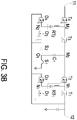
- the two different switch conditions are shown in FIGS. 3B and 3C .
- the voltage ratio of the switched-tank DC transformer 1 equals 3. Under this circumstance, the voltage ratio is reduced by 1 as compared with the voltage ratio of the switched-tank DC transformer 1 of FIG. 2A .
- the resonance tanks RT 1 , RT 2 are in the normal state.
- the first clamping switch S 1 and the second clamping switch S 2 are kept constantly in the OFF state, thus the first clamping node O 1 is kept constantly in the open-circuit condition.
- the second inverting switch T 2 and the third inverting switch T 3 are kept constantly in the ON state.
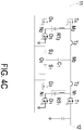
- the two different switch conditions are shown in FIGS. 4B and 4C .
- the voltage ratio of the switched-tank DC transformer 1 equals 2. Under this circumstance, the voltage ratio is reduced by 2 as compared with the voltage ratio of the switched-tank DC transformer 1 of FIG. 2A .
- the first resonance tank RT 1 or the second resonance tank RT 2 is switched from the normal state to the second voltage ratio switching state, so as to make the voltage ratio of the switched-tank DC transformer 1 equal to 2.
- the first clamping switch S 1 is kept constantly in the ON state
- the second clamping switch S 2 is kept constantly in the OFF state
- the first clamping node O 1 is kept constantly in electrical connection with the ground terminal.
- the third rectifying switch D 3 and the fourth rectifying switch D 4 are kept constantly in the OFF state, thus the second rectifying node N 2 is kept constantly in the open-circuit condition.
- the third inverting switch T 3 and the fourth inverting switch T 4 are kept constantly in the ON state.
- the voltage ratio of the switched-tank DC transformer 1 equals 1. Under this circumstance, the voltage ratio is reduced by 3 as compared with the voltage ratio of the switched-tank DC transformer 1 of FIG. 2A .
- the first support capacitor C 1 is switched from the normal state to the first voltage ratio switching state, and the first resonance tank RT 1 is switched from the normal state to the second voltage ratio switching state, so as to make the voltage ratio of the switched-tank DC transformer 1 equal to 1.
- FIG. 6 is a flowchart illustrating a voltage ratio switching method according an embodiment of the present disclosure.
- the voltage ratio switching method is applied to the switched-tank DC transformer 1 of FIG. 1 .
- the voltage ratio switching method controls the switch conditions of the support capacitors (C 1 , C 2 to C n-1 ) and the resonance tanks (RT 1 , RT 2 to RT n ), and further adjusts the voltage ratio of the switched-tank DC transformer 1.
- the voltage ratio switching method includes the following steps S1, S2, S3, S4 and S5.
- Step S1 Controlling the (i-1)th support capacitor C i-1 to be in the normal state, namely controlling the (i-1)th clamping node O i-1 to electrically connect the ground terminal and the output terminal 12 by turns.
- Step S2 Controlling the (i-1)th support capacitor C i-1 to be in the first voltage ratio switching state, namely controlling the (i-1)th clamping node O i-1 to be constantly in electrical connection with the ground terminal.
- the (2i-2)th clamping switch S 2i-2 is controlled to be constantly in the OFF state
- the (2i-3)th clamping switch S 2i-3 is controlled to be constantly in the ON state.
- Step S3 Controlling the (i-1)th support capacitor C i-1 to be in the second voltage ratio switching state, namely controlling the (i-1)th clamping node O i-1 to be constantly in the open-circuit condition, controlling the (2i)th inverting switch T 2i or the (2i-2)th inverting switch T 2i-2 to be constantly in the ON state, and controlling the (2i-1)th inverting switch T 2i-1 or the (2i-3)th inverting switch T 2i-3 to be constantly in the ON state.
- the (2i-2)th clamping switch S 2i-2 and the (2i-3)th clamping switch S 2i-3 are controlled to be constantly in the OFF state, thus the (i-1)th clamping node O i-1 is kept constantly in the open-circuit condition.
- Step S4 Controlling the (i)th resonance tank RT i to be in the normal state, namely controlling the (i)th rectifying node N i to electrically connect the output terminal 12 and the ground terminal by turns.
- Step S5 Controlling the (i)th resonance tank RT i to be in the second voltage ratio switching state, namely controlling the (i)th rectifying node N i to be constantly in the open-circuit condition, controlling the (2i+1)th inverting switch T 2i+1 or the (2i-1)th inverting switch T 2i-1 to be constantly in the ON state, and controlling the (2i)th inverting switch T 2i or the (2i-2)th inverting switch T 2i-2 to be constantly in the ON state.
- the (2i)th rectifying switch D 2i and the (2i-1)th rectifying switch D 2i-1 are controlled to be constantly in the OFF state, thus the (i)th rectifying node N i is kept constantly in the open-circuit condition.
- the step S4 further includes a step of controlling the first resonance tank RT 1 to be in the normal state, namely the first rectifying node N i is controlled to electrically connect the output terminal 12 and the ground terminal by turns.
- the step S5 further includes a step of controlling the first resonance tank RT 1 to be in the second voltage ratio switching state. Namely, the first rectifying node N 1 is controlled to be constantly in the open-circuit condition (for example, controlling the second rectifying switch D 2 and the first rectifying switch D 1 to be constantly in the OFF state).
- the third inverting switch T 3 or the first inverting switch T 1 is controlled to be constantly in the ON state.
- the second inverting switch T 2 is controlled to be constantly in the ON state.
- FIG. 6 only shows the steps included by the voltage ratio switching method. There is no order relationship among the steps S1, S2, S3, S4 and S5. One or plural of the steps can be performed in any order according to the actual requirements, and meanwhile the number of steps performed is not limited. Moreover, the above steps can be performed to one or plural support capacitor(s) (C 1 , C 2 to C n-1 ) and/or one or plural resonance tank(s) (RT 1 , RT 2 to RT n ). In addition, while the step(s) is/are performed, the effect on the voltage ratio of the switched-tank DC transformer 1 is described as follows.
- step S1 is performed to any support capacitor (C 1 , C 2 to C n-1 )
- step S2 is performed to that support capacitor (C 1 , C 2 to C n-1 )
- the voltage ratio of the switched-tank DC transformer 1 is subtracted by 1.
- step S2 is performed to any support capacitor (C 1 , C 2 to C n-1 )
- step S1 is performed to that support capacitor (C 1 , C 2 to C n-1 )
- the voltage ratio of the switched-tank DC transformer 1 is increased by 1.
- the voltage ratio of the switched-tank DC transformer 1 is allowed to vary between n+1 and 2n.
- step S1 is performed to any support capacitor (C 1 , C 2 to C n-1 )
- step S3 is performed to that support capacitor (C 1 , C 2 to C n-1 )
- the voltage ratio of the switched-tank DC transformer 1 is subtracted by 2.
- step S3 is performed to any support capacitor (C 1 , C 2 to C n-1 )
- the step S1 is performed to that support capacitor (C 1 , C 2 to C n-1 )
- the voltage ratio of the switched-tank DC transformer 1 is increased by 2. Since the n-1 support capacitors C 1 , C 2 to C n-1 can be switched between the normal state and the second voltage ratio switching state by the voltage ratio switching method, the voltage ratio of the switched-tank DC transformer 1 is allowed to vary between 2 and 2n.
- step S4 is performed to any resonance tank (RT 1 , RT 2 to RT n )
- step S5 is performed to that resonance tank (RT 1 , RT 2 to RT n )
- the voltage ratio of the switched-tank DC transformer 1 is subtracted by 2.
- the step S5 is performed to any resonance tank (RT 1 , RT 2 to RT n )
- the step S4 is performed to that resonance tank (RT 1 , RT 2 to RT n )
- the voltage ratio of the switched-tank DC transformer 1 is increased by 2. Since the n resonance tanks RT 1 , RT 2 to RT n can be switched between the normal state and the second voltage ratio switching state by the voltage ratio switching method, the voltage ratio of the switched-tank DC transformer 1 is allowed to vary between 2 and 2n.
- steps S1 and S4 are performed to A support capacitor(s) (C 1 , C 2 to C n-1 ) and B resonance tank(s) (RT 1 , RT 2 to RT n ) respectively
- steps S3 and S5 are performed to the A support capacitor(s) (C 1 , C 2 to C n-1 ) and the B resonance tank(s) (RT 1 , RT 2 to RT n ) respectively
- the voltage ratio of the switched-tank DC transformer 1 is subtracted by 2A+2B.
- the voltage ratio of the switched-tank DC transformer 1 is allowed to vary between 2 and 2n.
- steps S1 and S4 are performed to A support capacitor(s) (C 1 , C 2 to C n-1 ) and B resonance tank(s) (RT 1 , RT 2 to RT n ) respectively
- steps S2 and S5 are performed to the A support capacitor(s) (C 1 , C 2 to C n-1 ) and the B resonance tank(s) (RT 1 , RT 2 to RT n ) respectively
- the voltage ratio of the switched-tank DC transformer 1 is subtracted by A+2B.
- the voltage ratio of the switched-tank DC transformer 1 is allowed to vary between 1 and 2n.
- the present disclosure provides a switched-tank DC transformer and a voltage ratio switching method thereof.
- every support capacitor and every resonance tank is switchable to be in a normal state or a voltage ratio switching state. Accordingly, the voltage ratio of the switched-tank DC transformer is changed at will.
- the range of the output voltage can be limited by adjusting the voltage ratio of the switched-tank DC transformer. Therefore, both the high efficiency of power transformation and the adjustable output voltage are achieved.
- the voltage regulator module including the switched-tank DC transformer the efficiency and quality of supplying power thereof are enhanced.
Landscapes
- Engineering & Computer Science (AREA)
- Power Engineering (AREA)
- Dc-Dc Converters (AREA)
Abstract
Description
- The present disclosure relates to a switched-tank DC transformer, and more particularly to a switched-tank DC transformer and a voltage ratio switching method thereof.
- For ensuring the performance of the efficiency and quality of supplying power, the voltage regulator module (VRM) with intermediate bus architecture (IBA) is usually utilized for transforming the power. The intermediate bus architecture includes an intermediate bus transformer. Generally, the conventional intermediate bus transformer is a low-frequency switching DC transformer or a full-bridge LLC circuit. The low-frequency switching DC transformer regulates the output voltage by changing the duty ratio, thus the adjustable output voltage is achieved. The full-bridge LLC circuit can achieve zero-voltage switching (ZVS) over the full range. Therefore, by controlling the switching frequency to equal the resonance frequency of the tank of the full-bridge LLC circuit, the voltage ratio is ensured to be the same at different loads, and a high efficiency of power transformation is achieved.
- However, due to the high voltage ratio of the low-frequency switching DC transformer, the efficiency of power transformation thereof is low. In addition, due to the fixed voltage ratio of the full-bridge LLC circuit, the output voltage thereof is not adjustable. Consequently, neither the low-frequency switching DC transformer nor the full-bridge LLC circuit is able to achieve the high efficiency as well as the adjustable output voltage.
- Therefore, there is a need of providing a switched-tank DC transformer and a voltage ratio switching method thereof in order to overcome the above drawbacks.
- An object of the present disclosure provides a switched-tank DC transformer and a voltage ratio switching method thereof. In the switched-tank DC transformer, every support capacitor and every resonance tank is switchable to be in a normal state or a voltage ratio switching state. Accordingly, the voltage ratio of the switched-tank DC transformer is changed at will. When the input voltage varies in a wide range, the range of the output voltage can be limited by adjusting the voltage ratio of the switched-tank DC transformer. Therefore, both the high efficiency of power transformation and the adjustable output voltage are achieved. Moreover, with regard to the voltage regulator module including the switched-tank DC transformer, the efficiency and quality of supplying power thereof are enhanced.
- In accordance with an aspect of the present disclosure, there is provided a switched-tank DC transformer. The switched-tank DC transformer includes an input terminal, an output terminal, 2n inverting switches, 2n rectifying switches, 2n-2 clamping switches, n resonance tanks and n-1 support capacitors. The 2n inverting switches are serially connected in sequence and form n inverting half-bridge circuits, where n is an integer larger than or equal to 2. The first inverting switch is electrically connected with the output terminal, the (2n)th inverting switch is electrically connected with the input terminal, there is an inverting node between every two neighboring inverting switches, the (2i-1)th inverting node is between the (2i)th inverting switch and the (2i-1)th inverting switch, and i is an integer larger than or equal to 2 and smaller than or equal to n. The 2n rectifying switches form n rectifying half-bridge circuits sequentially. Each of the n rectifying half-bridge circuits includes two rectifying switches serially connected with each other, one terminal of both the two rectifying switches are electrically connected with a rectifying node, the other terminal of the two rectifying switches are electrically connected with a ground terminal and the output terminal respectively, and the (i)th rectifying node is between the (2i)th rectifying switch and the (2i-1)th rectifying switch. The 2n-2 clamping switches form n-1 clamping half-bridge circuits sequentially. Each of the n-1 clamping half-bridge circuits includes two clamping switches serially connected with each other, one terminal of both the two clamping switches are electrically connected with a clamping node, the other terminal of the two clamping switches are electrically connected with the ground terminal and the output terminal respectively, and the (i-1)th clamping node is between the (2i-2)th clamping switch and the (2i-3)th clamping switch. The resonance tank is electrically connected between the corresponding inverting node and the corresponding rectifying node, and the (i)th resonance tank is electrically connected between the (2i-1)th inverting node and the (i)th rectifying node. The support capacitor is electrically connected between the corresponding inverting node and the corresponding clamping node, and the (i-1)th support capacitor is electrically connected between the (2i-2)th inverting node and the (i-1)th clamping node. Each of the n-1 support capacitors is switchable to be in a normal state or a voltage ratio switching state, and each of the n resonance tanks is switchable to be in the normal state or the voltage ratio switching state, thus a voltage ratio of the switched-tank DC transformer is allowed to vary between 2 and 2n. When the (i-1)th support capacitor is in the normal state, the (i-1)th clamping node is electrically connected with the ground terminal and the output terminal by turns. When the (i-1)th support capacitor is in the voltage ratio switching state, the (i-1)th clamping node is kept constantly in an open-circuit condition, the (2i)th inverting switch or the (2i-2)th inverting switch is kept constantly in an ON state, the (2i-1)th inverting switch or the (2i-3)th inverting switch is kept constantly in the ON state. When the (i)th resonance tank is in the normal state, the (i)th rectifying node is electrically connected with the output terminal and the ground terminal by turns. When the (i)th resonance tank is in the voltage ratio switching state, the (i)th rectifying node is kept constantly in the open-circuit condition, the (2i+1)th inverting switch or the (2i-1)th inverting switch is kept constantly in the ON state, the (2i)th inverting switch or the (2i-2)th inverting switch is kept constantly in the ON state.
- In accordance with another aspect of the present disclosure, there is provided a voltage ratio switching method of a switched-tank DC transformer. The switched-tank DC transformer includes an input terminal, an output terminal, 2n inverting switches, 2n rectifying switches, 2n-2 clamping switches, n resonance tanks and n-1 support capacitors, where n is an integer larger than or equal to 2. The 2n inverting switches are serially connected in sequence and form n inverting half-bridge circuits, the first inverting switch is electrically connected with the output terminal, the (2n)th inverting switch is electrically connected with the input terminal, there is an inverting node between every two neighboring inverting switches, the (2i-1)th inverting node is between the (2i)th inverting switch and the (2i-1)th inverting switch, and i is an integer larger than or equal to 2 and smaller than or equal to n. The 2n rectifying switches form n rectifying half-bridge circuits sequentially, each of the n rectifying half-bridge circuits includes two rectifying switches serially connected with each other, one terminal of both the two rectifying switches are electrically connected with a rectifying node, the other terminal of the two rectifying switches are electrically connected with a ground terminal and the output terminal respectively, and the (i)th rectifying node is between the (2i)th rectifying switch and the (2i-1)th rectifying switch. The 2n-2 clamping switches form n-1 clamping half-bridge circuits sequentially, each of the n-1 clamping half-bridge circuits includes two clamping switches serially connected with each other, one terminal of both the two clamping switches are electrically connected with a clamping node, the other terminal of the two clamping switches are electrically connected with the ground terminal and the output terminal respectively, and the (i-1)th clamping node is between the (2i-2)th clamping switch and the (2i-3)th clamping switch. The resonance tank is electrically connected between the corresponding inverting node and the corresponding rectifying node, and the (i)th resonance tank is electrically connected between the (2i-1)th inverting node and the (i)th rectifying node. The support capacitor is electrically connected between the corresponding inverting node and the corresponding clamping node, and the (i-1)th support capacitor is electrically connected between the (2i-2)th inverting node and the (i-1)th clamping node. The voltage ratio switching method controls every support capacitor to be switchably in a normal state or a voltage ratio switching state. The voltage ratio switching method controls every resonance tank to be switchably in the normal state or the voltage ratio switching state. The voltage ratio switching method allows a voltage ratio of the switched-tank DC transformer to vary between 2 and 2n. The voltage ratio switching method includes: (a) controlling the (i-1)th support capacitor to be in the normal state, namely controlling the (i-1)th clamping node to electrically connect the ground terminal and the output terminal by turns; (b) controlling the (i-1)th support capacitor to be in the voltage ratio switching state, namely controlling the (i-1)th clamping node to be constantly in an open-circuit condition, controlling the (2i)th inverting switch or the (2i-2)th inverting switch to be constantly in an ON state, and controlling the (2i-1)th inverting switch or the (2i-3)th inverting switch to be constantly in the ON state; (c) controlling the (i)th resonance tank to be in the normal state, namely controlling the (i)th rectifying node to electrically connect the output terminal and the ground terminal by turns; and (d) controlling the (i)th resonance tank to be in the voltage ratio switching state, namely controlling the (i)th rectifying node to be constantly in the open-circuit condition, controlling the (2i+1)th inverting switch or the (2i-1)th inverting switch to be constantly in the ON state, and controlling the (2i)th inverting switch or the (2i-2)th inverting switch to be constantly in the ON state.
- The above contents of the present disclosure will become more readily apparent to those ordinarily skilled in the art after reviewing the following detailed description and accompanying drawings, in which:
-
-
FIG. 1 is a schematic circuit diagram illustrating a switched-tank DC transformer according to an embodiment of the present disclosure; -
FIG. 2A is a schematic circuit diagram illustrating the switched-tank DC transformer ofFIG. 1 with n equal to 2; -
FIGS. 2B and2C are schematic diagrams showing the different switch conditions of the switched-tank DC transformer ofFIG. 2A ; -
FIG. 3A is a schematic circuit diagram illustrating the switched-tank DC transformer ofFIG. 2A , wherein the support capacitor is in a first voltage ratio switching state, and the resonance tanks are in a normal state; -
FIGS. 3B and3C are schematic diagrams showing the different switch conditions of the switched-tank DC transformer ofFIG. 3A ; -
FIG. 4A is a schematic circuit diagram illustrating the switched-tank DC transformer ofFIG. 2A , wherein the support capacitor is in a second voltage ratio switching state, and the resonance tanks are in the normal state; -
FIGS. 4B and4C are schematic diagrams showing the different switch conditions of the switched-tank DC transformer ofFIG. 4A ; -
FIG. 5A is a schematic circuit diagram illustrating the switched-tank DC transformer ofFIG. 2A , wherein the support capacitor is in the first voltage ratio switching state, the first resonance tank is in the normal state, and the second resonance tank is in the second voltage ratio switching state; -
FIGS. 5B and5C are schematic diagrams showing the different switch conditions of the switched-tank DC transformer ofFIG. 5A ; and -
FIG. 6 is a flowchart illustrating a voltage ratio switching method according an embodiment of the present disclosure. - The present disclosure will now be described more specifically with reference to the following embodiments. It is to be noted that the following descriptions of preferred embodiments of this disclosure are presented herein for purpose of illustration and description only. It is not intended to be exhaustive or to be limited to the precise form disclosed.
-
FIG. 1 is a schematic circuit diagram illustrating a switched-tank DC transformer according to an embodiment of the present disclosure. As shown inFIG. 1 , the switched-tank DC transformer 1 includes aninput terminal 11, anoutput terminal 12, 2n inverting switches (T1, T2 to T2n), 2n rectifying switches (D1, D2 to D2n), 2n-2 clamping switches (S1, S2 to S2n-2), n resonance tanks (RT1, RT2 to RTn) and n-1 support capacitors (C1, C2 to Cn-1), where n is an integer larger than or equal to 2. There are an input voltage and an output voltage on theinput terminal 11 and theoutput terminal 12 respectively. The ratio of the input voltage to the output voltage is the voltage ratio of the switched-tank DC transformer 1. - The 2n inverting switches T1, T2 to T2n are serially connected in sequence and form n inverting half-bridge circuits. The first inverting switch T1 is electrically connected with the
output terminal 12, and the (2n)th inverting switch T2n is electrically connected with theinput terminal 11. There is an inverting node (M1, M2 to M2n-1) between every two neighboring inverting switches (T1, T2 to T2n). The first inverting node M1 is between the first inverting switch T1 and the second inverting switch T2. The second inverting node M2 is between the second inverting switch T2 and the third inverting switch T3. The (2n-1)th inverting node M2n-1 is between the (2n-1)th inverting switch T2n-1 and the (2n)th inverting switch T2n. On this basis, the (2i-1)th inverting node M2i-1 is between the (2i-1)th inverting switch T2i-1 and the (2i)th inverting switch T2i, where i is an integer larger than or equal to 2 and smaller than or equal to n. - The 2n rectifying switches D1, D2 to D2n form n rectifying half-bridge circuits sequentially. Each rectifying half-bridge circuit includes two rectifying switches (D1, D2 to D2n) serially connected with each other. One terminal of both the two rectifying switches (D1, D2 to D2n) are electrically connected with a rectifying node (N1, N2 to Nn), and the other terminal of the two rectifying switches (D1, D2 to D2n) are electrically connected with a ground terminal and the
output terminal 12 respectively. The first rectifying node N1 is between the first rectifying switch D1 and the second rectifying switch D2. The second rectifying node N2 is between the third rectifying switch D3 and the fourth rectifying switch D4. The (n)th rectifying node Nn is between the (2n-1)th rectifying switch D2n-1 and the (2n)th rectifying switch D2n. On this basis, the (i)th rectifying node Ni is between the (2i-1)th rectifying switch D2i-1 and the (2i)th rectifying switch D2i. - The 2n-2 clamping switches S1, S2 to S2n-2 form n-1 clamping half-bridge circuit(s) sequentially. Each clamping half-bridge circuit includes two clamping switches (S1, S2 to S2n-2) serially connected with each other. One terminal of both the two clamping switches (S1, S2 to S2n-2) are electrically connected with a clamping node (O1, O2 to On), and the other terminal of the two clamping switches (S1, S2 to S2n-2) are electrically connected with the ground terminal and the
output terminal 12 respectively. The first clamping node O1 is between the first clamping switch S1 and the second clamping switch S2. The second clamping node O2 is between the third clamping switch S3 and the fourth clamping switch S4. The (n-1)th clamping node On-1 is between the (2n-3)th clamping switch S2n-3 and the (2n-2)th clamping switch S2n-2. On this basis, the (i-1)th clamping node Oi-1 is between the (2i-3)th clamping switch S2i-3 and the (2i-2)th clamping switch S2i-2. - The resonance tank (RT1, RT2 to RTn) is electrically connected between the corresponding inverting node (M1, M2 to M2n-1) and the corresponding rectifying node (N1, N2 to Nn). The first resonance tank RT1 is electrically connected between the first inverting node M1 and the first rectifying node N1. The second resonance tank RT2 is electrically connected between the third inverting node M3 and the second rectifying node N2. The (n)th resonance tank RTn is electrically connected between the (2n-1)th inverting node M2n-1 and the (n)th rectifying node Nn. On this basis, the (i)th resonance tank RTi is electrically connected between the (2i-1)th inverting node M2i-1 and the (i)th rectifying node Ni. In an embodiment, each resonance tank (RT1, RT2 to RTn) includes an inductor and a capacitor serially connected with each other. In another embodiment, each resonance tank (RT1, RT2 to RTn) includes an inductor or a capacitor.
- The support capacitor (C1, C2 to Cn-1) is electrically connected between the corresponding inverting node (M1, M2 to M2n-1) and the corresponding clamping node (O1, O2 to On). The first support capacitor C1 is electrically connected between the second inverting node M2 and the first clamping node O1. The second support capacitor C2 is electrically connected between the fourth inverting node M4 and the second clamping node O2. The (n-1)th support capacitor Cn-1 is electrically connected between the (2n-2)th inverting node M2n-2 and the (n-1)th clamping node On-1. On this basis, the (i-1)th support capacitor Ci-1 is electrically connected between the (2i-2)th inverting node M2i-2 and the (i-1)th clamping node Oi-1.
- In the switched-
tank DC transformer 1, every support capacitor (C1, C2 to Cn-1) is switchable to be in a normal state, a first voltage ratio switching state or a second voltage ratio switching state, and every resonance tank (RT1, RT2 to RTn) is switchable to be in the normal state or the second voltage ratio switching state. Accordingly, the voltage ratio of the switched-tank DC transformer 1 is allowed to vary between 1 and 2n. When the input voltage varies in a wide range, the range of the output voltage is limited by adjusting the voltage ratio of the switched-tank DC transformer 1. Therefore, both the high efficiency of power transformation and the adjustable output voltage are achieved. According to the states of the support capacitors (C1, C2 to Cn-1) and the resonance tanks (RT1, RT2 to RTn), the operations of the nodes and switches of the switched-tank DC transformer 1 are described in detail as follows. - When the (i-1)th support capacitor Ci-1 is in the normal state, the (i-1)th clamping node Oi-1 is electrically connected with the ground terminal and the
output terminal 12 by turns. When the (i)th resonance tank RTi is in the normal state, the (i)th rectifying node Ni is electrically connected with theoutput terminal 12 and the ground terminal by turns. In an embodiment, when the first resonance RTi is in the normal state, the first rectifying node N1 is electrically connected with theoutput terminal 12 and the ground terminal by turns. In addition, when the (i-1)th support capacitor Ci-1 and the (i)th resonance tank RTi are both in the normal state, the (2i-2)th clamping switch S2i-2, the (2i-1)th inverting switch T2i-1 and the (2i-1)th rectifying switch D2i-1 are simultaneously in an ON state or an OFF state. Correspondingly, the (2i-3)th clamping switch S2i-3, the (2i)th inverting switch T2i and the (2i)th rectifying switch D2i are simultaneously in the OFF state or the ON state. In an embodiment, when the (i-1)th support capacitor Ci-1 and the (i)th resonance tank RTi are both in the normal state, the (2i-2)th clamping switch S2i-2 and the (2i-3)th clamping switch S2i-3 have opposite switch conditions and switch on by turns. The (2i-1)th inverting switch T2i-1 and the (2i)th inverting switch T2i have opposite switch conditions and switch on by turns. The (2i-1)th rectifying switch D2i-1 and the (2i)th rectifying switch D2i have opposite switch conditions and switch on by turns. - When the (i-1)th support capacitor Ci-1 is in the first voltage ratio switching state, the (i-1)th clamping node Oi-1 is kept constantly in electrical connection with the ground terminal. In an embodiment, when the (i-1)th support capacitor Ci-1 is in the first voltage ratio switching state, the (2i-2)th clamping switch S2i-2 is kept constantly in the OFF state, and the (2i-3)th clamping switch S2i-3 is kept constantly in the ON state. Consequently, the (i-1)th clamping node Oi-1 is kept constantly in electrical connection with the ground terminal.
- When the (i-1)th support capacitor Ci-1 is in the second voltage ratio switching state, the (i-1)th clamping node Oi-1 is kept constantly in an open-circuit condition, the (2i)th inverting switch T2i and the (2i-2)th inverting switch T2i-2 are kept constantly in the ON state, and the (2i-1)th inverting switch T2i-1 and the (2i-3)th inverting switch T2i-3 are kept constantly in the ON state. In an embodiment, when the (i-1)th support capacitor Ci-1 is in the second voltage ratio switching state, the (2i-2)th clamping switch S2i-2 and the (2i-3)th clamping switch S2i-3 are kept constantly in the OFF state. Consequently, the (i-1)th clamping node Oi-1 is kept constantly in the open-circuit condition.
- When the (i)th resonance tank RTi is in the second voltage ratio switching state, the (i)th rectifying node Ni is kept constantly in the open-circuit condition, the (2i+1)th inverting switch T2i+1 or the (2i-1)th inverting switch T2i-1 is kept constantly in the ON state, and the (2i)th inverting switch T2i or the (2i-2)th inverting switch T2i-2 are kept constantly in the ON state. In an embodiment, when the (i)th resonance tank RTi is in the second voltage ratio switching state, the (2i)th rectifying switch D2i and the (2i-1)th rectifying switch D2i-1 are kept constantly in the OFF state. Consequently, the (i)th rectifying node Ni is kept constantly in the open-circuit condition. In addition, when the first resonance tank RT1 is in the second voltage ratio switching state, the first rectifying node N1 is kept constantly in the open-circuit condition (for example, keeping the first rectifying switch D1 and the second rectifying switch D2 constantly in the OFF state). The third inverting switch T3 or the first inverting switch T1 is kept constantly in the ON state. The second inverting switch T2 is kept constantly in the ON state. When the (n)th resonance tank RTn is in the second voltage ratio switching state, the (n)th rectifying node Nn is kept constantly in the open-circuit condition (for example, keeping the (2n-1)th rectifying switch D2n-1 and the (2n)th rectifying switch D2n constantly in the OFF state). The (2n-1)th inverting switch T2n-1 is kept constantly in the ON state. The (2n)th inverting switch T2n or the (2n-2)th inverting switch T2n-2 is kept constantly in the ON state.
- Moreover, when the states of the support capacitor (C1, C2 to Cn-1) and/or the resonance tank (RT1, RT2 to RTn) are switched, the voltage ratio of the switched-
tank DC transformer 1 varies correspondingly. Some possible situations are listed as follows. - When any support capacitor (C1, C2 to Cn-1) is switched from the normal state to the first voltage ratio switching state, the voltage ratio of the switched-
tank DC transformer 1 is subtracted by 1. On the contrary, when any support capacitor (C1, C2 to Cn-1) is switched from the first voltage ratio switching state to the normal state, the voltage ratio of the switched-tank DC transformer 1 is increased by 1. Since the n-1 support capacitors C1, C2 to Cn-1 are all switchable to be in the normal state or the first voltage ratio switching state, the voltage ratio of the switched-tank DC transformer 1 is allowed to vary between (n+1) and 2n. - When any support capacitor (C1, C2 to Cn-1) or any resonance tank (RT1, RT2 to RTn) is switched from the normal state to the second voltage ratio switching state, the voltage ratio of the switched-
tank DC transformer 1 is subtracted by 2. On the contrary, when any support capacitor (C1, C2 to Cn-1) or any resonance tank (RT1, RT2 to RTn) is switched from the second voltage ratio switching state to the normal state, the voltage ratio of the switched-tank DC transformer 1 is increased by 2. Since the n-1 support capacitors C1, C2 to Cn-1 and the n resonance tanks RT1, RT2 to RTn are all switchable to be in the normal state or the second voltage ratio switching state, the voltage ratio of the switched-tank DC transformer 1 is allowed to vary between 2 and 2n. - When A support capacitor(s) (C1, C2 to Cn-1) is/are switched from the normal state to the first voltage ratio switching state, and B resonance tank(s) (RT1, RT2 to RTn) is/are switched from the normal state to the second voltage ratio switching state, the voltage ratio of the switched-
tank DC transformer 1 is subtracted by A+2B. On the contrary, when A support capacitor(s) (C1, C2 to Cn-1) is/are switched from the first voltage ratio switching state to the normal state, and B resonance tank(s) (RT1, RT2 to RTn) is/are switched from the second voltage ratio switching state to the normal state, the voltage ratio of the switched-tank DC transformer 1 is increased by A+2B. A is a natural number smaller than or equal to n-1, and B is a natural number smaller than or equal to n. Since the n-1 support capacitors C1, C2 to Cn-1 are switchable to be in the normal state or the first voltage ratio switching state, and the n resonance tanks RT1, RT2 to RTn are switchable to be in the normal state or the second voltage ratio switching state, the voltage ratio of the switched-tank DC transformer 1 is allowed to vary between 1 and 2n. - When A support capacitor(s) (C1, C2 to Cn-1) and B resonance tank(s) (RT1, RT2 to RTn) are switched from the normal state to the second voltage ratio switching state, the voltage ratio of the switched-
tank DC transformer 1 is subtracted by 2A+2B. On the contrary, when A support capacitor(s) (C1, C2 to Cn-1) and B resonance tank(s) (RT1, RT2 to RTn) are switched from the second voltage ratio switching state to the normal state, the voltage ratio of the switched-tank DC transformer 1 is increased by 2A+2B. Since the n-1 support capacitors C1, C2 to Cn-1 and the n resonance tanks RT1, RT2 to RTn are switchable to be in the normal state or the second voltage ratio switching state, the voltage ratio of the switched-tank DC transformer 1 is allowed to vary between 2 and 2n. - In order to be understood more easily, the switched-
tank DC transformer 1 with n equal to 2 is shown as an example, but the switched-tank DC transformer of the present disclosure is not limited thereto.FIG. 2A is a schematic circuit diagram illustrating the switched-tank DC transformer ofFIG. 1 with n equal to 2.FIGS. 2B and2C are schematic diagrams showing the different switch conditions of the switched-tank DC transformer ofFIG. 2A . As shown inFIG. 2A , in this embodiment, n equals 2, and the switched-tank DC transformer 1 includes aninput terminal 11, anoutput terminal 12, four inverting switches T1, T2, T3, T4, four rectifying switches D1, D2, D3, D4, two clamping switches S1, S2, two resonance tanks RT1, RT2 and one support capacitor C1. As shown in the schematic diagrams of different switch conditions (seeFIGS. 2B and2C ), the part of the circuit that the current not passing through is depicted by relatively thin lines. Therefore, the current path under different switch conditions can be recognized and distinguished. As shown inFIGS. 2B and2C , when the support capacitor C1 and the resonance tanks RT1, RT2 are all in the normal state, the first clamping switch S1, the second inverting switch T2, the fourth inverting switch T4, the second rectifying switch D2 and the fourth rectifying switch D4 are simultaneously in the ON state or the OFF state. Correspondingly, the second clamping switch S2, the first inverting switch T1, the third inverting switch T3, the first rectifying switch D1 and the third rectifying switch D3 are simultaneously in the OFF state or the ON state. In particular, the first clamping switch S1 and the second clamping switch S2 have opposite switch conditions and switch on by turns. The first inverting switch T1 and the second inverting switch T2 have opposite switch conditions and switch on by turns. The third inverting switch T3 and the fourth inverting switch T4 have opposite switch conditions and switch on by turns. The first rectifying switch D1 and the second rectifying switch D2 have opposite switch conditions and switch on by turns. The third rectifying switch D3 and the fourth rectifying switch D4 have opposite switch conditions and switch on by turns. - In this embodiment, by switching the states of the support capacitor C1 and the resonance tanks RT1, RT2, the voltage ratio of the switched-
tank DC transformer 1 is allowed to vary between 1 and 4. Some specific examples are shown as follows. However, in the actual applications, the way of switching the states of the support capacitor C1 and the resonance tanks RT1, RT2 is not limited thereto. - Under the circumstance that the first support capacitor C1 is switched from the normal state to the first voltage ratio switching state, and the resonance tanks RT1, RT2 are in the normal state. As shown in
FIG. 3A , the first clamping switch S1 is kept constantly in the ON state, the second clamping switch S2 is kept constantly in the OFF state, thus the first clamping node O1 is kept constantly in electrical connection with the ground terminal. The two different switch conditions are shown inFIGS. 3B and3C . The voltage ratio of the switched-tank DC transformer 1 equals 3. Under this circumstance, the voltage ratio is reduced by 1 as compared with the voltage ratio of the switched-tank DC transformer 1 ofFIG. 2A . - Under the circumstance that the first support capacitor C1 is switched from the normal state to the second voltage ratio switching state, and the resonance tanks RT1, RT2 are in the normal state. As shown in
FIG. 4A , the first clamping switch S1 and the second clamping switch S2 are kept constantly in the OFF state, thus the first clamping node O1 is kept constantly in the open-circuit condition. The second inverting switch T2 and the third inverting switch T3 are kept constantly in the ON state. The two different switch conditions are shown inFIGS. 4B and4C . The voltage ratio of the switched-tank DC transformer 1 equals 2. Under this circumstance, the voltage ratio is reduced by 2 as compared with the voltage ratio of the switched-tank DC transformer 1 ofFIG. 2A . Alternatively, in an embodiment, the first resonance tank RT1 or the second resonance tank RT2 is switched from the normal state to the second voltage ratio switching state, so as to make the voltage ratio of the switched-tank DC transformer 1 equal to 2. - Under the circumstance that the first support capacitor C1 is switched from the normal state to the first voltage ratio switching state, and the second resonance tank RT2 is switched from the normal state to the second voltage ratio switching state. As shown in
FIG. 5A , the first clamping switch S1 is kept constantly in the ON state, the second clamping switch S2 is kept constantly in the OFF state, thus the first clamping node O1 is kept constantly in electrical connection with the ground terminal. The third rectifying switch D3 and the fourth rectifying switch D4 are kept constantly in the OFF state, thus the second rectifying node N2 is kept constantly in the open-circuit condition. The third inverting switch T3 and the fourth inverting switch T4 are kept constantly in the ON state. The two different switch conditions are shown inFIGS. 5B and5C . The voltage ratio of the switched-tank DC transformer 1 equals 1. Under this circumstance, the voltage ratio is reduced by 3 as compared with the voltage ratio of the switched-tank DC transformer 1 ofFIG. 2A . Alternatively, in an embodiment, the first support capacitor C1 is switched from the normal state to the first voltage ratio switching state, and the first resonance tank RT1 is switched from the normal state to the second voltage ratio switching state, so as to make the voltage ratio of the switched-tank DC transformer 1 equal to 1. -
FIG. 6 is a flowchart illustrating a voltage ratio switching method according an embodiment of the present disclosure. The voltage ratio switching method is applied to the switched-tank DC transformer 1 ofFIG. 1 . The voltage ratio switching method controls the switch conditions of the support capacitors (C1, C2 to Cn-1) and the resonance tanks (RT1, RT2 to RTn), and further adjusts the voltage ratio of the switched-tank DC transformer 1. The voltage ratio switching method includes the following steps S1, S2, S3, S4 and S5. - Step S1:Controlling the (i-1)th support capacitor Ci-1 to be in the normal state, namely controlling the (i-1)th clamping node Oi-1 to electrically connect the ground terminal and the
output terminal 12 by turns. - Step S2:Controlling the (i-1)th support capacitor Ci-1 to be in the first voltage ratio switching state, namely controlling the (i-1)th clamping node Oi-1 to be constantly in electrical connection with the ground terminal. In an embodiment, the (2i-2)th clamping switch S2i-2 is controlled to be constantly in the OFF state, and the (2i-3)th clamping switch S2i-3 is controlled to be constantly in the ON state.
- Step S3:Controlling the (i-1)th support capacitor Ci-1 to be in the second voltage ratio switching state, namely controlling the (i-1)th clamping node Oi-1 to be constantly in the open-circuit condition, controlling the (2i)th inverting switch T2i or the (2i-2)th inverting switch T2i-2 to be constantly in the ON state, and controlling the (2i-1)th inverting switch T2i-1 or the (2i-3)th inverting switch T2i-3 to be constantly in the ON state. In an embodiment, the the (2i-2)th clamping switch S2i-2 and the (2i-3)th clamping switch S2i-3 are controlled to be constantly in the OFF state, thus the (i-1)th clamping node Oi-1 is kept constantly in the open-circuit condition.
- Step S4:Controlling the (i)th resonance tank RTi to be in the normal state, namely controlling the (i)th rectifying node Ni to electrically connect the
output terminal 12 and the ground terminal by turns. - Step S5:Controlling the (i)th resonance tank RTi to be in the second voltage ratio switching state, namely controlling the (i)th rectifying node Ni to be constantly in the open-circuit condition, controlling the (2i+1)th inverting switch T2i+1 or the (2i-1)th inverting switch T2i-1 to be constantly in the ON state, and controlling the (2i)th inverting switch T2i or the (2i-2)th inverting switch T2i-2 to be constantly in the ON state. In an embodiment, the (2i)th rectifying switch D2i and the (2i-1)th rectifying switch D2i-1 are controlled to be constantly in the OFF state, thus the (i)th rectifying node Ni is kept constantly in the open-circuit condition.
- In an embodiment, the step S4 further includes a step of controlling the first resonance tank RT1 to be in the normal state, namely the first rectifying node Ni is controlled to electrically connect the
output terminal 12 and the ground terminal by turns. In an embodiment, the step S5 further includes a step of controlling the first resonance tank RT1 to be in the second voltage ratio switching state. Namely, the first rectifying node N1 is controlled to be constantly in the open-circuit condition (for example, controlling the second rectifying switch D2 and the first rectifying switch D1 to be constantly in the OFF state). The third inverting switch T3 or the first inverting switch T1 is controlled to be constantly in the ON state. The second inverting switch T2 is controlled to be constantly in the ON state. - It is noted that
FIG. 6 only shows the steps included by the voltage ratio switching method. There is no order relationship among the steps S1, S2, S3, S4 and S5. One or plural of the steps can be performed in any order according to the actual requirements, and meanwhile the number of steps performed is not limited. Moreover, the above steps can be performed to one or plural support capacitor(s) (C1, C2 to Cn-1) and/or one or plural resonance tank(s) (RT1, RT2 to RTn). In addition, while the step(s) is/are performed, the effect on the voltage ratio of the switched-tank DC transformer 1 is described as follows. - After the step S1 is performed to any support capacitor (C1, C2 to Cn-1), if the step S2 is performed to that support capacitor (C1, C2 to Cn-1), the voltage ratio of the switched-
tank DC transformer 1 is subtracted by 1. On the contrary, after the step S2 is performed to any support capacitor (C1, C2 to Cn-1), if the step S1 is performed to that support capacitor (C1, C2 to Cn-1), the voltage ratio of the switched-tank DC transformer 1 is increased by 1. Since the n-1 support capacitors C1, C2 to Cn-1 can be switched between the normal state and the first voltage ratio switching state by the voltage ratio switching method, the voltage ratio of the switched-tank DC transformer 1 is allowed to vary between n+1 and 2n. - After the step S1 is performed to any support capacitor (C1, C2 to Cn-1), if the step S3 is performed to that support capacitor (C1, C2 to Cn-1), the voltage ratio of the switched-
tank DC transformer 1 is subtracted by 2. On the contrary, after the step S3 is performed to any support capacitor (C1, C2 to Cn-1), if the step S1 is performed to that support capacitor (C1, C2 to Cn-1), the voltage ratio of the switched-tank DC transformer 1 is increased by 2. Since the n-1 support capacitors C1, C2 to Cn-1 can be switched between the normal state and the second voltage ratio switching state by the voltage ratio switching method, the voltage ratio of the switched-tank DC transformer 1 is allowed to vary between 2 and 2n. - After the step S4 is performed to any resonance tank (RT1, RT2 to RTn), if the step S5 is performed to that resonance tank (RT1, RT2 to RTn), the voltage ratio of the switched-
tank DC transformer 1 is subtracted by 2. On the contrary, after the step S5 is performed to any resonance tank (RT1, RT2 to RTn), if the step S4 is performed to that resonance tank (RT1, RT2 to RTn), the voltage ratio of the switched-tank DC transformer 1 is increased by 2. Since the n resonance tanks RT1, RT2 to RTn can be switched between the normal state and the second voltage ratio switching state by the voltage ratio switching method, the voltage ratio of the switched-tank DC transformer 1 is allowed to vary between 2 and 2n. - After the steps S1 and S4 are performed to A support capacitor(s) (C1, C2 to Cn-1) and B resonance tank(s) (RT1, RT2 to RTn) respectively, if the steps S3 and S5 are performed to the A support capacitor(s) (C1, C2 to Cn-1) and the B resonance tank(s) (RT1, RT2 to RTn) respectively, the voltage ratio of the switched-
tank DC transformer 1 is subtracted by 2A+2B. On the contrary, after the steps S3 and S5 are performed to A support capacitor(s) (C1, C2 to Cn-1) and B resonance tank(s) (RT1, RT2 to RTn) respectively, if the steps S1 and S4 are performed to the A support capacitor(s) (C1, C2 to Cn-1) and the B resonance tank(s) (RT1, RT2 to RTn) respectively, the voltage ratio of the switched-tank DC transformer 1 is increased by 2A+2B. A is a natural number smaller than or equal to n-1, and B is a natural number smaller than or equal to n. Since the n-1 support capacitors C1, C2 to Cn-1 and the n resonance tanks RT1, RT2 to RTn can be switched between the normal state and the second voltage ratio switching state by the voltage ratio switching method, the voltage ratio of the switched-tank DC transformer 1 is allowed to vary between 2 and 2n. - After the steps S1 and S4 are performed to A support capacitor(s) (C1, C2 to Cn-1) and B resonance tank(s) (RT1, RT2 to RTn) respectively, if the steps S2 and S5 are performed to the A support capacitor(s) (C1, C2 to Cn-1) and the B resonance tank(s) (RT1, RT2 to RTn) respectively, the voltage ratio of the switched-
tank DC transformer 1 is subtracted by A+2B. On the contrary, after the steps S2 and S5 are performed to A support capacitor(s) (C1, C2 to Cn-1) and B resonance tank(s) (RT1, RT2 to RTn) respectively, if the steps S1 and S4 are performed to the A support capacitor(s) (C1, C2 to Cn-1) and the B resonance tank(s) (RT1, RT2 to RTn) respectively, the voltage ratio of the switched-tank DC transformer 1 is increased by A+2B. Since the n-1 support capacitors C1, C2 to Cn-1 and the n resonance tanks RT1, RT2 to RTn can be switched between the normal state and the first voltage ratio switching state by the voltage ratio switching method, the voltage ratio of the switched-tank DC transformer 1 is allowed to vary between 1 and 2n. - From the above descriptions, the present disclosure provides a switched-tank DC transformer and a voltage ratio switching method thereof. In the switched-tank DC transformer, every support capacitor and every resonance tank is switchable to be in a normal state or a voltage ratio switching state. Accordingly, the voltage ratio of the switched-tank DC transformer is changed at will. When the input voltage varies in a wide range, the range of the output voltage can be limited by adjusting the voltage ratio of the switched-tank DC transformer. Therefore, both the high efficiency of power transformation and the adjustable output voltage are achieved. Moreover, with regard to the voltage regulator module including the switched-tank DC transformer, the efficiency and quality of supplying power thereof are enhanced.
- While the disclosure has been described in terms of what is presently considered to be the most practical and preferred embodiments, it is to be understood that the disclosure needs not be limited to the disclosed embodiment. On the contrary, it is intended to cover various modifications and similar arrangements included within the spirit and scope of the appended claims which are to be accorded with the broadest interpretation so as to encompass all such modifications and similar structures.
Claims (15)
- A switched-tank DC transformer (1), comprising:an input terminal (11) and an output terminal (12);2n inverting switches serially connected to form n inverting half-bridge circuits, wherein n is an integer larger than or equal to 2, the first inverting switch (T1) is electrically connected with the output terminal (12), the (2n)th inverting switch (T2n) is electrically connected with the input terminal (11), there is an inverting node between every two neighboring inverting switches, the (2i-1)th inverting node (M2i-1) is between the (2i)th inverting switch (T2i) and the (2i-1)th inverting switch (T2i-1), and i is an integer larger than or equal to 2 and smaller than or equal to n;2n rectifying switches forming n rectifying half-bridge circuits sequentially, wherein each of the n rectifying half-bridge circuits comprises two rectifying switches serially connected with each other, one terminal of both the two rectifying switches are electrically connected with a rectifying node, the other terminal of the two rectifying switches are electrically connected with a ground terminal and the output terminal (12) respectively, and the (i)th rectifying node (Ni) is between the (2i)th rectifying switch (D2i) and the (2i-1)th rectifying switch (D2i-1);2n-2 clamping switches forming n-1 clamping half-bridge circuits sequentially, wherein each of the n-1 clamping half-bridge circuits comprises two clamping switches serially connected with each other, one terminal of both the two clamping switches are electrically connected with a clamping node, the other terminal of the two clamping switches are electrically connected with the ground terminal and the output terminal (12) respectively, and the (i-1)th clamping node (Oi-1) is between the (2i-2)th clamping switch (S2i-2) and the (2i-3)th clamping switch (S2i-3);n resonance tanks, wherein the resonance tank is electrically connected between the corresponding inverting node and the corresponding rectifying node, and the (i)th resonance tank (RTi) is electrically connected between the (2i-1)th inverting node (M2i-1) and the (i)th rectifying node (Ni); andn-1 support capacitors, wherein the support capacitor is electrically connected between the corresponding inverting node and the corresponding clamping node, and the (i-1)th support capacitor (Ci-1) is electrically connected between the (2i-2)th inverting node (M2i-2) and the (i-1)th clamping node (Oi-1),wherein each of the n-1 support capacitors is switchable to be in a normal state or a voltage ratio switching state, each of the n resonance tanks is switchable to be in the normal state or the voltage ratio switching state, thus a voltage ratio of the switched-tank DC transformer (1) is allowed to vary between 2 and 2n,when the (i-1)th support capacitor (Ci-1) is in the normal state, the (i-1)th clamping node (Oi-1) is electrically connected with the ground terminal and the output terminal (12) by turns; when the (i-1)th support capacitor (Ci-1) is in the voltage ratio switching state, the (i-1)th clamping node (Oi-1) is kept constantly in an open-circuit condition, the (2i)th inverting switch (T2i) or the (2i-2)th inverting switch (T2i-2) is kept constantly in an ON state, the (2i-1)th inverting switch (T2i-1) or the (2i-3)th inverting switch (T2i-3) is kept constantly in the ON state,when the (i)th resonance tank (RTi) is in the normal state, the (i)th rectifying node (Ni) is electrically connected with the output terminal (12) and the ground terminal by turns; when the (i)th resonance tank (RTi) is in the voltage ratio switching state, the (i)th rectifying node (Ni) is kept constantly in the open-circuit condition, the (2i+1)th inverting switch (T2i+1) or the (2i-1)th inverting switch (T2i-1) is kept constantly in the ON state, the (2i)th inverting switch (T2i) or the (2i-2)th inverting switch (T2i-2) is kept constantly in the ON state.
- The switched-tank DC transformer (1) according to claim 1, wherein when the first resonance tank (RT1) is in the normal state, the first rectifying node (N1) is electrically connected with the output terminal (12) and the ground terminal by turns; wherein when the first resonance tank (RT1) is in the voltage ratio switching state, the first rectifying node (N1) is kept constantly in the open-circuit condition, the third inverting switch (T3) or the first inverting switch (T1) is kept constantly in the ON state, and the second inverting switch (T2) is kept constantly in the ON state.
- The switched-tank DC transformer (1) according to claim 1, wherein when the (i-1)th support capacitor (Ci-1) and the (i)th resonance tank (RTi) are both in the normal state, the (2i-2)th clamping switch (S2i-2), the (2i-1)th inverting switch (T2i-1) and the (2i-1)th rectifying switch (D2i-1) are simultaneously in the ON state or a OFF state, and the (2i-3)th clamping switch (S2i-3), the (2i)th inverting switch (T2i) and the (2i)th rectifying switch (D2i) are simultaneously in the OFF state or the ON state correspondingly, and the (2i-2)th clamping switch (S2i-2) and the (2i-3)th clamping switch (S2i-3) have opposite switch conditions and switch on by turns; the (2i-1)th inverting switch (T2i-1) and the (2i)th inverting switch (T2i) have opposite switch conditions and switch on by turns; and the (2i-1)th rectifying switch (D2i-1) and the (2i)th rectifying switch (D2i) have opposite switch conditions and switch on by turns.
- The switched-tank DC transformer (1) according to claim 1, wherein when the (i-1)th support capacitor (Ci-1) is in the voltage ratio switching state, the (2i-2)th clamping switch (S2i-2) and the (2i-3)th clamping switch (S2i-3) are kept constantly in an OFF state, the (2i)th inverting switch (T2i) or the (2i-2)th inverting switch (T2i-2) is kept constantly in the ON state, and the (2i-1)th inverting switch (T2i-1) or the (2i-3)th inverting switch (T2i-3) is kept constantly in the ON state.
- The switched-tank DC transformer (1) according to claim 1, wherein when the (i)th resonance tank (RTi) is in the voltage ratio switching state, the (2i)th rectifying switch (D2i) and the (2i-1)th rectifying switch (D2i-1) are kept constantly in a OFF state, the (2i+1)th inverting switch (T2i+1) or the (2i-1)th inverting switch (T2i-1) is kept constantly in the ON state, and the (2i)th inverting switch (T2i) or the (2i-2)th inverting switch (T2i-2) is kept constantly in the ON state.
- The switched-tank DC transformer (1) according to claim 1, wherein when the first resonance tank (RT1) is in the voltage ratio switching state, the second rectifying switch (D2) and the first rectifying switch (D1) are kept constantly in an OFF state, the third inverting switch (T3) or the first inverting switch (T1) is kept constantly in the ON state, and the second inverting switch (T2) is kept constantly in the ON state.
- The switched-tank DC transformer (1) according to claim 1, wherein when any of the support capacitors or any of the resonance tanks is switched from the normal state to the voltage ratio switching state, the voltage ratio of the switched-tank DC transformer (1) is subtracted by 2, and when any of the support capacitors or any of the resonance tanks is switched from the voltage ratio switching state to the normal state, the voltage ratio of the switched-tank DC transformer (1) is increased by 2,
wherein when A support capacitor(s) and B resonance tank(s) are switched from the normal state to the voltage ratio switching state, the voltage ratio of the switched-tank DC transformer (1) is subtracted by 2A+2B, when A support capacitor(s) and B resonance tank(s) are switched from the voltage ratio switching state to the normal state, the voltage ratio of the switched-tank DC transformer (1) is increased by 2A+2B, and A is a natural number smaller than or equal to n-1, B is a natural number smaller than or equal to n. - A voltage ratio switching method of a switched-tank DC transformer (1), wherein the switched-tank DC transformer (1) comprises an input terminal (11), an output terminal (12), 2n inverting switches, 2n rectifying switches, 2n-2 clamping switches, n resonance tanks and n-1 support capacitors, n is an integer larger than or equal to 2, the 2n inverting switches are serially connected to form n inverting half-bridge circuits, the first inverting switch (T1) is electrically connected with the output terminal (12), the (2n)th inverting switch (T2n) is electrically connected with the input terminal (11), there is an inverting node between every two neighboring inverting switches, the (2i-1)th inverting node (M2i-1) is between the (2i)th inverting switch (T2i) and the (2i-1)th inverting switch (T2i-1), and i is an integer larger than or equal to 2 and smaller than or equal to n; the 2n rectifying switches form n rectifying half-bridge circuits sequentially, each of the n rectifying half-bridge circuits comprises two rectifying switches serially connected with each other, one terminal of both the two rectifying switches are electrically connected with a rectifying node, the other terminal of the two rectifying switches are electrically connected with a ground terminal and the output terminal (12) respectively, and the (i)th rectifying node (Ni) is between the (2i)th rectifying switch (D2i) and the (2i-1)th rectifying switch (D2i-1); the 2n-2 clamping switches form n-1 clamping half-bridge circuits sequentially, each of the n-1 clamping half-bridge circuits comprises two clamping switches serially connected with each other, one terminal of both the two clamping switches are electrically connected with a clamping node, the other terminal of the two clamping switches are electrically connected with the ground terminal and the output terminal (12) respectively, and the (i-1)th clamping node (Oi-1) is between the (2i-2)th clamping switch (S2i-2) and the (2i-3)th clamping switch (S2i-3); the resonance tank is electrically connected between the corresponding inverting node and the corresponding rectifying node, and the (i)th resonance tank (RTi) is electrically connected between the (2i-1)th inverting node (M2i-1) and the (i)th rectifying node (Ni); and the support capacitor is electrically connected between the corresponding inverting node and the corresponding clamping node, and the (i-1)th support capacitor (Ci-1) is electrically connected between the (2i-2)th inverting node (M2i-1) and the (i-1)th clamping node (Oi-1),
the voltage ratio switching method controlling every support capacitor to be switchably in a normal state or a voltage ratio switching state, the voltage ratio switching method controlling every resonance tank to be switchably in the normal state or the voltage ratio switching state, the voltage ratio switching method allowing a voltage ratio of the switched-tank DC transformer (1) to vary between 2 and 2n, the voltage ratio switching method comprising:(a) controlling the (i-1)th support capacitor (Ci-1) to be in the normal state, namely controlling the (i-1)th clamping node to electrically connect the ground terminal and the output terminal by turns;(b) controlling the (i-1)th support capacitor (Ci-1) to be in the voltage ratio switching state, namely controlling the (i-1)th clamping node (Oi-1) to be constantly in an open-circuit condition, controlling the (2i)th inverting switch (T2i) or the (2i-2)th inverting switch (T2i-2) to be constantly in an ON state, and controlling the (2i-1)th inverting switch (T2i-1) or the (2i-3)th inverting switch (T2i-3) to be constantly in the ON state;(c) controlling the (i)th resonance tank (RTi) to be in the normal state, namely controlling the (i)th rectifying node (Ni) to electrically connect the output terminal (12) and the ground terminal by turns; and(d) controlling the (i)th resonance tank (RTi) to be in the voltage ratio switching state, namely controlling the (i)th rectifying node (Ni) to be constantly in the open-circuit condition, controlling the (2i+1)th inverting switch (T2i+1) or the (2i-1)th inverting switch (T2i-1) to be constantly in the ON state, and controlling the (2i)th inverting switch (T2i) or the (2i-2)th inverting switch (T2i-2) to be constantly in the ON state. - The voltage ratio switching method according to claim 8,
wherein the step (c) further comprises a step of controlling the first resonance tank (RT1) to be in the normal state, namely the first rectifying node(N1) is controlled to electrically connect the output terminal (12) and the ground terminal by turns; and
wherein the step (d) further comprises a step of controlling the first resonance tank (RT1) to be in the voltage ratio switching state, namely, the first rectifying node(N1) is controlled to be constantly in the open-circuit condition, the third inverting switch (T3) or the first inverting switch(T1) is controlled to be constantly in the ON state, and the second inverting switch(T2) is controlled to be constantly in the ON state. - The voltage ratio switching method according to claim 8, wherein when the (i-1)th support capacitor (Ci-1) and the (i)th resonance tank (RTi) are both in the normal state, the (2i-2)th clamping switch (S2i-2), the (2i-1)th inverting switch (T2i-1) and the (2i-1)th rectifying switch (D2i-1) are simultaneously in the ON state or an OFF state, and the (2i-3)th clamping switch (S2i-3), the (2i)th inverting switch (T2i) and the (2i)th rectifying switch (D2i) are simultaneously in the OFF state or the ON state correspondingly, and the (2i-2)th clamping switch (S2i-2) and the (2i-3)th clamping switch (S2i-3) have opposite switch conditions and switch on by turns; the (2i-1)th inverting switch (T2i-1) and the (2i)th inverting switch (T2i) have opposite switch conditions and switch on by turns; and the (2i-1)th rectifying switch (D2i-1) and the (2i)th rectifying switch (D2i) have opposite switch conditions and switch on by turns.
- The voltage ratio switching method according to claim 8, wherein in the step (b), the (2i-2)th clamping switch (S2i-2) and the (2i-3)th clamping switch (S2i-3) are controlled to be constantly in an OFF state, the (2i)th inverting switch (T2i) or the (2i-2)th inverting switch (T2i-2) is controlled to be constantly in the ON state, and the (2i-1)th inverting switch (T2i-1) or the (2i-3)th inverting switch (T2i-3) is controlled to be constantly in the ON state.
- The voltage ratio switching method according to claim 8, wherein in the step (d), the (2i)th rectifying switch (D2i) and the (2i-1)th rectifying switch (D2i-1) are controlled to be constantly in an OFF state, the (2i+1)th inverting switch (T2i+1) or the (2i-1)th inverting switch (T2i-1) is controlled to be constantly in the ON state, and the (2i)th inverting switch (T2i) or the (2i-2)th inverting switch (T2i-2) is controlled to be constantly in the ON state,
wherein the step (d) further comprises: controlling the second rectifying switch (D2) and the first rectifying switch (D1) to be constantly in an OFF state, controlling the third inverting switch (T3) or the first inverting switch (T1) to be constantly in the ON state, and controlling the second inverting switch (T2) to be constantly in the ON state. - The voltage ratio switching method according to claim 8, wherein after performing the step (a) to any of the support capacitors, if the step (b) is performed to that support capacitor, the voltage ratio of the switched-tank DC transformer (1) is subtracted by 2, and wherein after performing the step (b) to any of the support capacitors, if the step (a) is performed to that support capacitor, the voltage ratio of the switched-tank DC transformer (1) is increased by 2.
- The voltage ratio switching method according to claim 8 wherein after performing the step (c) to any of the resonance tanks, if the step (d) is performed to that resonance tank, the voltage ratio of the switched-tank DC transformer (1) is subtracted by 2, and wherein after performing the step (d) to any of the resonance tanks, if the step (c) is performed to that resonance tank, the voltage ratio of the switched-tank DC transformer (1) is increased by 2.
- The voltage ratio switching method according to claim 8 wherein after performing the steps (a) and (c) to A support capacitor(s) and B resonance tank(s) respectively, if the steps (b) and (d) are performed to the A support capacitor(s) and the B resonance tank(s) respectively, the voltage ratio of the switched-tank DC transformer (1) is subtracted by 2A+2B, wherein after performing the steps (b) and (d) to A support capacitor(s) and B resonance tank(s) respectively, if the steps (a) and (c) are performed to the A support capacitor(s) and the B resonance tank(s) respectively, the voltage ratio of the switched-tank DC transformer (1) is increased by 2A+2B, and A is a natural number smaller than or equal to n-1, B is a natural number smaller than or equal to n.
Applications Claiming Priority (1)
| Application Number | Priority Date | Filing Date | Title |
|---|---|---|---|
| CN201811338938.9A CN111181403B (en) | 2018-11-12 | 2018-11-12 | Switch resonant cavity direct current converter and transformation ratio switching method thereof |
Publications (2)
| Publication Number | Publication Date |
|---|---|
| EP3657656A1 true EP3657656A1 (en) | 2020-05-27 |
| EP3657656B1 EP3657656B1 (en) | 2021-06-02 |
Family
ID=68502937
Family Applications (1)
| Application Number | Title | Priority Date | Filing Date |
|---|---|---|---|
| EP19207742.8A Active EP3657656B1 (en) | 2018-11-12 | 2019-11-07 | Switched-tank dc transformer and voltage ratio switching method thereof |
Country Status (3)
| Country | Link |
|---|---|
| US (1) | US10879808B2 (en) |
| EP (1) | EP3657656B1 (en) |
| CN (1) | CN111181403B (en) |
Families Citing this family (6)
| Publication number | Priority date | Publication date | Assignee | Title |
|---|---|---|---|---|
| CN111416518B (en) * | 2019-01-07 | 2023-10-03 | 马克西姆综合产品公司 | Variable switching frequency switching energy storage converter and related method |
| US11290008B2 (en) * | 2019-03-29 | 2022-03-29 | Mediatek Singapore Pte. Ltd. | Resonant switched-capacitor converter |
| TWI740619B (en) * | 2020-08-21 | 2021-09-21 | 國立臺灣科技大學 | Control circuit and control method for power converter |
| EP4207569A4 (en) * | 2020-09-01 | 2023-10-25 | Huawei Digital Power Technologies Co., Ltd. | DC/DC CONVERTER AND VOLTAGE GAIN CHANGING METHOD AND SYSTEM |
| CN113746326B (en) * | 2021-09-07 | 2024-05-28 | 上海伏达半导体有限公司 | Switched capacitor converter and method |
| US11855536B2 (en) * | 2021-09-23 | 2023-12-26 | Psemi Corporation | Power converters, power systems, and switch topologies |
Citations (1)
| Publication number | Priority date | Publication date | Assignee | Title |
|---|---|---|---|---|
| US9966842B1 (en) * | 2017-08-16 | 2018-05-08 | Google Llc | Parallel voltage regulator with switched capacitor or capacitor-inductor blocks |
Family Cites Families (17)
| Publication number | Priority date | Publication date | Assignee | Title |
|---|---|---|---|---|
| CN101534104A (en) * | 2009-04-01 | 2009-09-16 | 电子科技大学 | Miniature ultra wide band electrically tunable filter |
| CN103326580B (en) | 2011-12-01 | 2016-08-24 | 台达电子企业管理(上海)有限公司 | DC-to-DC converter, power converter and control method thereof |
| CN103701331B (en) * | 2013-12-24 | 2016-08-17 | 深圳开立生物医疗科技股份有限公司 | The LLC mode of resonance wide-voltage range output high-efficiency power of resonant frequency can be changed |
| US9985516B2 (en) * | 2014-02-12 | 2018-05-29 | Palo Alto Research Center Incorporated | DC/DC converter and method for zero voltage switching |
| AU2015244410A1 (en) * | 2014-04-09 | 2016-11-10 | Lionel O. Barthold | Multi-module dc-to-dc power transformation system |
| WO2016149319A1 (en) * | 2015-03-16 | 2016-09-22 | Finsix Corporation | Control of resonant power converters |
| CN204538976U (en) | 2015-04-26 | 2015-08-05 | 中国计量学院 | Realize 1/2 nthe variable stage switching capacity type AC-AC converter of no-load voltage ratio |
| CN204696926U (en) | 2015-06-19 | 2015-10-07 | 正德职业技术学院 | A kind of adjustable compression set LLC resonant converter frequently |
| US10879805B2 (en) * | 2015-09-22 | 2020-12-29 | Infineon Technologies Austria Ag | System and method for a switched-mode power supply having a transformer with a plurality of primary windings |
| CN106558994B (en) * | 2015-09-30 | 2020-03-13 | 株式会社村田制作所 | DC/DC converter |
| US9831776B1 (en) * | 2016-06-16 | 2017-11-28 | Google Inc. | DC-DC converter |
| CN106130356B (en) | 2016-07-13 | 2018-12-18 | 上海交通大学 | Regulation method based on the adjustable wide input LLC resonant converter of transformer voltage ratio |
| KR101776770B1 (en) * | 2016-09-08 | 2017-09-08 | 현대자동차 주식회사 | Dc-dc converter and control method thereof |
| US9917517B1 (en) * | 2016-10-26 | 2018-03-13 | Google Inc. | Switched tank converter |
| CN106655788A (en) * | 2016-12-30 | 2017-05-10 | 上海联影医疗科技有限公司 | Resonant converter |
| CN107395010B (en) | 2017-06-20 | 2019-04-23 | 天津大学 | Interleaved parallel switched capacitor type wide-gain bidirectional DC converter for energy storage systems |
| CN108696140A (en) | 2018-06-08 | 2018-10-23 | 山东大学 | Full-bridge resonance DC-DC converter with wide output voltage range and modulator approach |
-
2018
- 2018-11-12 CN CN201811338938.9A patent/CN111181403B/en active Active
-
2019
- 2019-11-06 US US16/676,382 patent/US10879808B2/en active Active
- 2019-11-07 EP EP19207742.8A patent/EP3657656B1/en active Active
Patent Citations (1)
| Publication number | Priority date | Publication date | Assignee | Title |
|---|---|---|---|---|
| US9966842B1 (en) * | 2017-08-16 | 2018-05-08 | Google Llc | Parallel voltage regulator with switched capacitor or capacitor-inductor blocks |
Also Published As
| Publication number | Publication date |
|---|---|
| US10879808B2 (en) | 2020-12-29 |
| CN111181403A (en) | 2020-05-19 |
| EP3657656B1 (en) | 2021-06-02 |
| CN111181403B (en) | 2021-03-09 |
| US20200153347A1 (en) | 2020-05-14 |
Similar Documents
| Publication | Publication Date | Title |
|---|---|---|
| EP3657656B1 (en) | Switched-tank dc transformer and voltage ratio switching method thereof | |
| EP3657655B1 (en) | Switched-tank dc transformer and voltage ratio switching method thereof | |
| JP6951222B2 (en) | Power converter and power conversion system | |
| US11641164B2 (en) | Power conversion circuit and power conversion apparatus with same | |
| CN113179020B (en) | Multi-phase current-sharing interleaved parallel LLC resonant converter device and implementation method | |
| US20130162048A1 (en) | Power module and multi power supply apparatus having the same | |
| US9837906B1 (en) | Multiphase DCDC converter with asymmetric GM | |
| US11894765B2 (en) | Power conversion device | |
| US9690311B2 (en) | Power supply apparatus | |
| US20200153331A1 (en) | Power device | |
| US10164544B2 (en) | Isolated partial power converter | |
| US11336187B2 (en) | Resonant switching converter | |
| US12580489B2 (en) | DC/DC converter and control method thereof | |
| CN104702115A (en) | Method of equally dividing power of input-parallel output-parallel modularized DC (Direct Current) converter | |
| RU2391763C2 (en) | Unit of supply from circuit with full bridge circuit and wide control range | |
| CN111030469B (en) | High-voltage power supply circuit | |
| CN212231338U (en) | Intermediate-power multi-path voltage output open-loop half-bridge resonant circuit based on IR2153S | |
| WO2008029343A2 (en) | Resonant power converter | |
| Noah et al. | Review of current balance mechanism in multiphase LLC resonant converters | |
| CN118920825A (en) | Voltage equalizing control circuit, source load system and electronic equipment | |
| CN113612393B (en) | Power supply circuit, direct current power supply and photovoltaic system | |
| CN118076995A (en) | Display device and display control method | |
| US20220376628A1 (en) | Apparatus and method for dc-to-dc conversion | |
| US20240243602A1 (en) | Charging Circuit and Charger | |
| CN115622410B (en) | Switch resonant tank conversion circuit, chip, mainboard and electronic equipment |
Legal Events
| Date | Code | Title | Description |
|---|---|---|---|
| PUAI | Public reference made under article 153(3) epc to a published international application that has entered the european phase |
Free format text: ORIGINAL CODE: 0009012 |
|
| STAA | Information on the status of an ep patent application or granted ep patent |
Free format text: STATUS: THE APPLICATION HAS BEEN PUBLISHED |
|
| AK | Designated contracting states |
Kind code of ref document: A1 Designated state(s): AL AT BE BG CH CY CZ DE DK EE ES FI FR GB GR HR HU IE IS IT LI LT LU LV MC MK MT NL NO PL PT RO RS SE SI SK SM TR |
|
| AX | Request for extension of the european patent |
Extension state: BA ME |
|
| STAA | Information on the status of an ep patent application or granted ep patent |
Free format text: STATUS: REQUEST FOR EXAMINATION WAS MADE |
|
| 17P | Request for examination filed |
Effective date: 20200604 |
|
| RBV | Designated contracting states (corrected) |
Designated state(s): AL AT BE BG CH CY CZ DE DK EE ES FI FR GB GR HR HU IE IS IT LI LT LU LV MC MK MT NL NO PL PT RO RS SE SI SK SM TR |
|
| GRAP | Despatch of communication of intention to grant a patent |
Free format text: ORIGINAL CODE: EPIDOSNIGR1 |
|
| STAA | Information on the status of an ep patent application or granted ep patent |
Free format text: STATUS: GRANT OF PATENT IS INTENDED |
|
| INTG | Intention to grant announced |
Effective date: 20201023 |
|
| GRAS | Grant fee paid |
Free format text: ORIGINAL CODE: EPIDOSNIGR3 |
|
| GRAJ | Information related to disapproval of communication of intention to grant by the applicant or resumption of examination proceedings by the epo deleted |
Free format text: ORIGINAL CODE: EPIDOSDIGR1 |
|
| GRAL | Information related to payment of fee for publishing/printing deleted |
Free format text: ORIGINAL CODE: EPIDOSDIGR3 |
|
| STAA | Information on the status of an ep patent application or granted ep patent |
Free format text: STATUS: REQUEST FOR EXAMINATION WAS MADE |
|
| INTC | Intention to grant announced (deleted) | ||
| GRAP | Despatch of communication of intention to grant a patent |
Free format text: ORIGINAL CODE: EPIDOSNIGR1 |
|
| STAA | Information on the status of an ep patent application or granted ep patent |
Free format text: STATUS: GRANT OF PATENT IS INTENDED |
|
| GRAA | (expected) grant |
Free format text: ORIGINAL CODE: 0009210 |
|
| STAA | Information on the status of an ep patent application or granted ep patent |
Free format text: STATUS: THE PATENT HAS BEEN GRANTED |
|
| INTG | Intention to grant announced |
Effective date: 20210416 |
|
| REG | Reference to a national code |
Ref country code: CH Ref legal event code: EP |
|
| AK | Designated contracting states |
Kind code of ref document: B1 Designated state(s): AL AT BE BG CH CY CZ DE DK EE ES FI FR GB GR HR HU IE IS IT LI LT LU LV MC MK MT NL NO PL PT RO RS SE SI SK SM TR |
|
| REG | Reference to a national code |
Ref country code: GB Ref legal event code: FG4D |
|
| REG | Reference to a national code |
Ref country code: AT Ref legal event code: REF Ref document number: 1399370 Country of ref document: AT Kind code of ref document: T Effective date: 20210615 |
|
| REG | Reference to a national code |
Ref country code: IE Ref legal event code: FG4D |
|
| REG | Reference to a national code |
Ref country code: DE Ref legal event code: R096 Ref document number: 602019005071 Country of ref document: DE |
|
| REG | Reference to a national code |
Ref country code: NL Ref legal event code: FP |
|
| REG | Reference to a national code |
Ref country code: LT Ref legal event code: MG9D |
|
| PG25 | Lapsed in a contracting state [announced via postgrant information from national office to epo] |
Ref country code: LT Free format text: LAPSE BECAUSE OF FAILURE TO SUBMIT A TRANSLATION OF THE DESCRIPTION OR TO PAY THE FEE WITHIN THE PRESCRIBED TIME-LIMIT Effective date: 20210602 Ref country code: HR Free format text: LAPSE BECAUSE OF FAILURE TO SUBMIT A TRANSLATION OF THE DESCRIPTION OR TO PAY THE FEE WITHIN THE PRESCRIBED TIME-LIMIT Effective date: 20210602 Ref country code: FI Free format text: LAPSE BECAUSE OF FAILURE TO SUBMIT A TRANSLATION OF THE DESCRIPTION OR TO PAY THE FEE WITHIN THE PRESCRIBED TIME-LIMIT Effective date: 20210602 Ref country code: BG Free format text: LAPSE BECAUSE OF FAILURE TO SUBMIT A TRANSLATION OF THE DESCRIPTION OR TO PAY THE FEE WITHIN THE PRESCRIBED TIME-LIMIT Effective date: 20210902 |
|
| REG | Reference to a national code |
Ref country code: AT Ref legal event code: MK05 Ref document number: 1399370 Country of ref document: AT Kind code of ref document: T Effective date: 20210602 |
|
| PG25 | Lapsed in a contracting state [announced via postgrant information from national office to epo] |
Ref country code: RS Free format text: LAPSE BECAUSE OF FAILURE TO SUBMIT A TRANSLATION OF THE DESCRIPTION OR TO PAY THE FEE WITHIN THE PRESCRIBED TIME-LIMIT Effective date: 20210602 Ref country code: SE Free format text: LAPSE BECAUSE OF FAILURE TO SUBMIT A TRANSLATION OF THE DESCRIPTION OR TO PAY THE FEE WITHIN THE PRESCRIBED TIME-LIMIT Effective date: 20210602 Ref country code: LV Free format text: LAPSE BECAUSE OF FAILURE TO SUBMIT A TRANSLATION OF THE DESCRIPTION OR TO PAY THE FEE WITHIN THE PRESCRIBED TIME-LIMIT Effective date: 20210602 Ref country code: NO Free format text: LAPSE BECAUSE OF FAILURE TO SUBMIT A TRANSLATION OF THE DESCRIPTION OR TO PAY THE FEE WITHIN THE PRESCRIBED TIME-LIMIT Effective date: 20210902 Ref country code: PL Free format text: LAPSE BECAUSE OF FAILURE TO SUBMIT A TRANSLATION OF THE DESCRIPTION OR TO PAY THE FEE WITHIN THE PRESCRIBED TIME-LIMIT Effective date: 20210602 Ref country code: GR Free format text: LAPSE BECAUSE OF FAILURE TO SUBMIT A TRANSLATION OF THE DESCRIPTION OR TO PAY THE FEE WITHIN THE PRESCRIBED TIME-LIMIT Effective date: 20210903 |
|
| PG25 | Lapsed in a contracting state [announced via postgrant information from national office to epo] |
Ref country code: SK Free format text: LAPSE BECAUSE OF FAILURE TO SUBMIT A TRANSLATION OF THE DESCRIPTION OR TO PAY THE FEE WITHIN THE PRESCRIBED TIME-LIMIT Effective date: 20210602 Ref country code: EE Free format text: LAPSE BECAUSE OF FAILURE TO SUBMIT A TRANSLATION OF THE DESCRIPTION OR TO PAY THE FEE WITHIN THE PRESCRIBED TIME-LIMIT Effective date: 20210602 Ref country code: ES Free format text: LAPSE BECAUSE OF FAILURE TO SUBMIT A TRANSLATION OF THE DESCRIPTION OR TO PAY THE FEE WITHIN THE PRESCRIBED TIME-LIMIT Effective date: 20210602 Ref country code: AT Free format text: LAPSE BECAUSE OF FAILURE TO SUBMIT A TRANSLATION OF THE DESCRIPTION OR TO PAY THE FEE WITHIN THE PRESCRIBED TIME-LIMIT Effective date: 20210602 Ref country code: CZ Free format text: LAPSE BECAUSE OF FAILURE TO SUBMIT A TRANSLATION OF THE DESCRIPTION OR TO PAY THE FEE WITHIN THE PRESCRIBED TIME-LIMIT Effective date: 20210602 Ref country code: PT Free format text: LAPSE BECAUSE OF FAILURE TO SUBMIT A TRANSLATION OF THE DESCRIPTION OR TO PAY THE FEE WITHIN THE PRESCRIBED TIME-LIMIT Effective date: 20211004 Ref country code: RO Free format text: LAPSE BECAUSE OF FAILURE TO SUBMIT A TRANSLATION OF THE DESCRIPTION OR TO PAY THE FEE WITHIN THE PRESCRIBED TIME-LIMIT Effective date: 20210602 Ref country code: SM Free format text: LAPSE BECAUSE OF FAILURE TO SUBMIT A TRANSLATION OF THE DESCRIPTION OR TO PAY THE FEE WITHIN THE PRESCRIBED TIME-LIMIT Effective date: 20210602 |
|
| REG | Reference to a national code |
Ref country code: DE Ref legal event code: R097 Ref document number: 602019005071 Country of ref document: DE |
|
| PLBE | No opposition filed within time limit |
Free format text: ORIGINAL CODE: 0009261 |
|
| STAA | Information on the status of an ep patent application or granted ep patent |
Free format text: STATUS: NO OPPOSITION FILED WITHIN TIME LIMIT |
|
| PG25 | Lapsed in a contracting state [announced via postgrant information from national office to epo] |
Ref country code: DK Free format text: LAPSE BECAUSE OF FAILURE TO SUBMIT A TRANSLATION OF THE DESCRIPTION OR TO PAY THE FEE WITHIN THE PRESCRIBED TIME-LIMIT Effective date: 20210602 |
|
| 26N | No opposition filed |
Effective date: 20220303 |
|
| PG25 | Lapsed in a contracting state [announced via postgrant information from national office to epo] |
Ref country code: AL Free format text: LAPSE BECAUSE OF FAILURE TO SUBMIT A TRANSLATION OF THE DESCRIPTION OR TO PAY THE FEE WITHIN THE PRESCRIBED TIME-LIMIT Effective date: 20210602 |
|
| PG25 | Lapsed in a contracting state [announced via postgrant information from national office to epo] |
Ref country code: MC Free format text: LAPSE BECAUSE OF FAILURE TO SUBMIT A TRANSLATION OF THE DESCRIPTION OR TO PAY THE FEE WITHIN THE PRESCRIBED TIME-LIMIT Effective date: 20210602 |
|
| PG25 | Lapsed in a contracting state [announced via postgrant information from national office to epo] |
Ref country code: LU Free format text: LAPSE BECAUSE OF NON-PAYMENT OF DUE FEES Effective date: 20211107 Ref country code: IT Free format text: LAPSE BECAUSE OF FAILURE TO SUBMIT A TRANSLATION OF THE DESCRIPTION OR TO PAY THE FEE WITHIN THE PRESCRIBED TIME-LIMIT Effective date: 20210602 Ref country code: BE Free format text: LAPSE BECAUSE OF NON-PAYMENT OF DUE FEES Effective date: 20211130 |
|
| REG | Reference to a national code |
Ref country code: BE Ref legal event code: MM Effective date: 20211130 |
|
| PG25 | Lapsed in a contracting state [announced via postgrant information from national office to epo] |
Ref country code: IE Free format text: LAPSE BECAUSE OF NON-PAYMENT OF DUE FEES Effective date: 20211107 |
|
| PG25 | Lapsed in a contracting state [announced via postgrant information from national office to epo] |
Ref country code: FR Free format text: LAPSE BECAUSE OF NON-PAYMENT OF DUE FEES Effective date: 20211130 |
|
| PG25 | Lapsed in a contracting state [announced via postgrant information from national office to epo] |
Ref country code: CY Free format text: LAPSE BECAUSE OF FAILURE TO SUBMIT A TRANSLATION OF THE DESCRIPTION OR TO PAY THE FEE WITHIN THE PRESCRIBED TIME-LIMIT Effective date: 20210602 |
|
| REG | Reference to a national code |
Ref country code: CH Ref legal event code: PL |
|
| PG25 | Lapsed in a contracting state [announced via postgrant information from national office to epo] |
Ref country code: LI Free format text: LAPSE BECAUSE OF NON-PAYMENT OF DUE FEES Effective date: 20221130 Ref country code: HU Free format text: LAPSE BECAUSE OF FAILURE TO SUBMIT A TRANSLATION OF THE DESCRIPTION OR TO PAY THE FEE WITHIN THE PRESCRIBED TIME-LIMIT; INVALID AB INITIO Effective date: 20191107 Ref country code: CH Free format text: LAPSE BECAUSE OF NON-PAYMENT OF DUE FEES Effective date: 20221130 |
|
| PG25 | Lapsed in a contracting state [announced via postgrant information from national office to epo] |
Ref country code: MK Free format text: LAPSE BECAUSE OF FAILURE TO SUBMIT A TRANSLATION OF THE DESCRIPTION OR TO PAY THE FEE WITHIN THE PRESCRIBED TIME-LIMIT Effective date: 20210602 |
|
| GBPC | Gb: european patent ceased through non-payment of renewal fee |
Effective date: 20231107 |
|
| PG25 | Lapsed in a contracting state [announced via postgrant information from national office to epo] |
Ref country code: MT Free format text: LAPSE BECAUSE OF FAILURE TO SUBMIT A TRANSLATION OF THE DESCRIPTION OR TO PAY THE FEE WITHIN THE PRESCRIBED TIME-LIMIT Effective date: 20210602 |
|
| PG25 | Lapsed in a contracting state [announced via postgrant information from national office to epo] |
Ref country code: GB Free format text: LAPSE BECAUSE OF NON-PAYMENT OF DUE FEES Effective date: 20231107 |
|
| PG25 | Lapsed in a contracting state [announced via postgrant information from national office to epo] |
Ref country code: GB Free format text: LAPSE BECAUSE OF NON-PAYMENT OF DUE FEES Effective date: 20231107 |
|
| PGFP | Annual fee paid to national office [announced via postgrant information from national office to epo] |
Ref country code: NL Payment date: 20250912 Year of fee payment: 7 |
|
| PG25 | Lapsed in a contracting state [announced via postgrant information from national office to epo] |
Ref country code: TR Free format text: LAPSE BECAUSE OF FAILURE TO SUBMIT A TRANSLATION OF THE DESCRIPTION OR TO PAY THE FEE WITHIN THE PRESCRIBED TIME-LIMIT Effective date: 20210602 |
|
| PGFP | Annual fee paid to national office [announced via postgrant information from national office to epo] |
Ref country code: DE Payment date: 20250910 Year of fee payment: 7 |