EP3657182A1 - Dynamic calibration of current sense for switching converters - Google Patents
Dynamic calibration of current sense for switching converters Download PDFInfo
- Publication number
- EP3657182A1 EP3657182A1 EP19200143.6A EP19200143A EP3657182A1 EP 3657182 A1 EP3657182 A1 EP 3657182A1 EP 19200143 A EP19200143 A EP 19200143A EP 3657182 A1 EP3657182 A1 EP 3657182A1
- Authority
- EP
- European Patent Office
- Prior art keywords
- voltage
- calibration
- transistor
- gain
- current
- Prior art date
- Legal status (The legal status is an assumption and is not a legal conclusion. Google has not performed a legal analysis and makes no representation as to the accuracy of the status listed.)
- Granted
Links
Images



Classifications
-
- G—PHYSICS
- G01—MEASURING; TESTING
- G01R—MEASURING ELECTRIC VARIABLES; MEASURING MAGNETIC VARIABLES
- G01R35/00—Testing or calibrating of apparatus covered by the other groups of this subclass
- G01R35/02—Testing or calibrating of apparatus covered by the other groups of this subclass of auxiliary devices, e.g. of instrument transformers according to prescribed transformation ratio, phase angle, or wattage rating
-
- G—PHYSICS
- G01—MEASURING; TESTING
- G01R—MEASURING ELECTRIC VARIABLES; MEASURING MAGNETIC VARIABLES
- G01R19/00—Arrangements for measuring currents or voltages or for indicating presence or sign thereof
- G01R19/0092—Measuring current only
-
- G—PHYSICS
- G01—MEASURING; TESTING
- G01R—MEASURING ELECTRIC VARIABLES; MEASURING MAGNETIC VARIABLES
- G01R35/00—Testing or calibrating of apparatus covered by the other groups of this subclass
- G01R35/005—Calibrating; Standards or reference devices, e.g. voltage or resistance standards, "golden" references
-
- G—PHYSICS
- G01—MEASURING; TESTING
- G01R—MEASURING ELECTRIC VARIABLES; MEASURING MAGNETIC VARIABLES
- G01R19/00—Arrangements for measuring currents or voltages or for indicating presence or sign thereof
- G01R19/32—Compensating for temperature change
-
- G—PHYSICS
- G01—MEASURING; TESTING
- G01R—MEASURING ELECTRIC VARIABLES; MEASURING MAGNETIC VARIABLES
- G01R19/00—Arrangements for measuring currents or voltages or for indicating presence or sign thereof
- G01R19/25—Arrangements for measuring currents or voltages or for indicating presence or sign thereof using digital measurement techniques
- G01R19/2513—Arrangements for monitoring electric power systems, e.g. power lines or loads; Logging
-
- G—PHYSICS
- G01—MEASURING; TESTING
- G01R—MEASURING ELECTRIC VARIABLES; MEASURING MAGNETIC VARIABLES
- G01R31/00—Arrangements for testing electric properties; Arrangements for locating electric faults; Arrangements for electrical testing characterised by what is being tested not provided for elsewhere
- G01R31/40—Testing power supplies
-
- H—ELECTRICITY
- H02—GENERATION; CONVERSION OR DISTRIBUTION OF ELECTRIC POWER
- H02M—APPARATUS FOR CONVERSION BETWEEN AC AND AC, BETWEEN AC AND DC, OR BETWEEN DC AND DC, AND FOR USE WITH MAINS OR SIMILAR POWER SUPPLY SYSTEMS; CONVERSION OF DC OR AC INPUT POWER INTO SURGE OUTPUT POWER; CONTROL OR REGULATION THEREOF
- H02M1/00—Details of apparatus for conversion
- H02M1/0003—Details of control, feedback or regulation circuits
- H02M1/0009—Devices or circuits for detecting current in a converter
-
- H—ELECTRICITY
- H02—GENERATION; CONVERSION OR DISTRIBUTION OF ELECTRIC POWER
- H02M—APPARATUS FOR CONVERSION BETWEEN AC AND AC, BETWEEN AC AND DC, OR BETWEEN DC AND DC, AND FOR USE WITH MAINS OR SIMILAR POWER SUPPLY SYSTEMS; CONVERSION OF DC OR AC INPUT POWER INTO SURGE OUTPUT POWER; CONTROL OR REGULATION THEREOF
- H02M1/00—Details of apparatus for conversion
- H02M1/0003—Details of control, feedback or regulation circuits
- H02M1/0012—Control circuits using digital or numerical techniques
-
- H—ELECTRICITY
- H02—GENERATION; CONVERSION OR DISTRIBUTION OF ELECTRIC POWER
- H02M—APPARATUS FOR CONVERSION BETWEEN AC AND AC, BETWEEN AC AND DC, OR BETWEEN DC AND DC, AND FOR USE WITH MAINS OR SIMILAR POWER SUPPLY SYSTEMS; CONVERSION OF DC OR AC INPUT POWER INTO SURGE OUTPUT POWER; CONTROL OR REGULATION THEREOF
- H02M3/00—Conversion of DC power input into DC power output
- H02M3/02—Conversion of DC power input into DC power output without intermediate conversion into AC
- H02M3/04—Conversion of DC power input into DC power output without intermediate conversion into AC by static converters
- H02M3/10—Conversion of DC power input into DC power output without intermediate conversion into AC by static converters using discharge tubes with control electrode or semiconductor devices with control electrode
- H02M3/145—Conversion of DC power input into DC power output without intermediate conversion into AC by static converters using discharge tubes with control electrode or semiconductor devices with control electrode using devices of a triode or transistor type requiring continuous application of a control signal
- H02M3/155—Conversion of DC power input into DC power output without intermediate conversion into AC by static converters using discharge tubes with control electrode or semiconductor devices with control electrode using devices of a triode or transistor type requiring continuous application of a control signal using semiconductor devices only
- H02M3/156—Conversion of DC power input into DC power output without intermediate conversion into AC by static converters using discharge tubes with control electrode or semiconductor devices with control electrode using devices of a triode or transistor type requiring continuous application of a control signal using semiconductor devices only with automatic control of output voltage or current, e.g. switching regulators
- H02M3/158—Conversion of DC power input into DC power output without intermediate conversion into AC by static converters using discharge tubes with control electrode or semiconductor devices with control electrode using devices of a triode or transistor type requiring continuous application of a control signal using semiconductor devices only with automatic control of output voltage or current, e.g. switching regulators including plural semiconductor devices as final control devices for a single load
Definitions
- This disclosure relates generally to temperature compensation, and more specifically to temperature compensation of an output stage of a Pulse Width Modulated (PWM) power converter.
- PWM Pulse Width Modulated
- Switching converters typically convert a variable input voltage to supply a regulated power output over a wide temperature range. Regulation of the supplied power may include monitoring output current and/or voltage characteristics to regulate a switching frequency of a PWM stage designed to switch power Field Effect Transistors (FETs). For proper power regulation, the temperature dependence of the power FETs requires compensation.
- FETs Field Effect Transistors
- a system for dynamic calibration of current sense for switching converters comprising:
- each of the current sense channels may comprise a transconductance amplifier configured to sense the respective transistor voltage, a Multiplying Digital to Analog Converter configured to multiply an amplifier output current of the transconductance amplifier by the gain to provide a calibration current, and the calibration resistor configured to sink the calibration current to generate the calibration voltage.
- a latch may be configured to store an averaged gain coefficient of a plurality of samples of the gain coefficient, and the gain of the first one and the second one of the current sense channels is determined by the averaged gain coefficient.
- the system may further comprise a load inductor connected between the phase node and a load capacitor, wherein a regulated voltage of the switching converter is formed on the load capacitor.
- the target voltage may be determined by measuring a respective calibration voltage of the third one of the current sense channels corresponding the respective transistor biased to the first voltage and an average target current flowing though the load inductor.
- the gain coefficient is determined while the ZTC current source is activated with a pulsed source.
- a method for dynamic calibration of current sense for switching converters comprising: biasing a reference transistor with a Zero Temperature Coefficient (ZTC) current source, and a respective gate of each of the reference transistor and a power transistor with a gate voltage, wherein each of the reference transistor and the power transistor comprises a matching temperature coefficient; multiplying a reference voltage sensed across the reference transistor by a first gain, thereby generating a first calibration voltage, wherein the first gain is determined by a gain coefficient; multiplying a transistor voltage sensed across the power transistor by the first gain, thereby generating a second calibration voltage; comparing the first calibration voltage to a target voltage to generate an error voltage; and determining the gain coefficient with an Analog to Digital Converter in response to the error voltage, thereby minimizing the error voltage and a difference between the target voltage and each of the first calibration voltage and the second calibration voltage.
- ZTC Zero Temperature Coefficient
- the method may further comprise activating the ZTC current source with a pulsed current source, wherein the gain coefficient is determined while the ZTC current source is activated.
- generating the first calibration voltage may further comprise sensing the reference voltage with a transconductance amplifier, converting an amplifier output of the transconductance amplifier with a Multiplying Digital to Analog Converter (MDAC) controlled by the first gain and generating the first calibration voltage by sinking an calibration current generated by the MDAC through a calibration resistor.
- MDAC Multiplying Digital to Analog Converter
- the method may further comprise compensating for a difference in a transistor gain between the reference transistor and the power transistor by changing a second gain of the MDAC.
- the method may further comprise compensating for a difference in a transistor gain between the reference transistor and the power transistor by changing a first resistance value of the calibration resistor used to determine the first calibration voltage relative to a second resistance value of a second calibration resistor used to determine the second calibration voltage.
- the method may further comprise deactivating the transconductance amplifier in response to deactivating the power transistor.
- the method may further comprise determining the target voltage by measuring the first calibration voltage corresponding to the reference transistor biased by the gate voltage and an average target current flowing through a load inductor connected between a load capacitor and the power transistor.
- an apparatus for dynamic calibration of current sense for switching converters comprising: a first one of a plurality of current sense channels configured to multiply by a first gain, a first voltage sensed between a first drain and a first source of a first transistor, and to generate a first calibration voltage therefrom, wherein the first gain is defined by a gain coefficient, and wherein a first gate voltage on a first gate of the first transistor controls a first current flowing between the first drain and the first source; a second one of the plurality of current sense channels configured to multiply by the first gain, a second voltage sensed between a second drain and a second source of a second transistor, and to generate a second calibration voltage therefrom, the second drain connected to a Zero Temperature Coefficient (ZTC) current source, the second source connected to a ground, a second gate of the second transistor biased to the first gate voltage and a first temperature coefficient of the first transistor equal to a second temperature coefficient of the second transistor; a comparator configured to generate an error voltage from a difference
- ZTC Zero Temperature Co
- each of the current sense channels may comprise a respective transconductance amplifier configured to sense a respective voltage between a respective drain and a respective source of the respective transistor, a respective Multiplying Digital to Analog Converter configured to multiply a respective amplifier output current of the respective transconductance amplifier by the first gain to provide a respective calibration current, and a respective calibration resistor configured to sink the respective calibration current to generate the respective calibration voltage.
- each of the respective calibration resistors of the current sense channels may have a same resistance.
- a first transistor gain of the first transistor may be greater than a second transistor gain of the second transistor, thereby reducing a second transistor current.
- a difference between the first transistor gain and the second transistor gain is compensated by a proportional change in a second gain of a respective Multiplying Digital to Analog Converter (MDAC) of the first one of the plurality of current sense channels, wherein the respective MDAC is configured to multiply the first voltage by the first gain to generate the first calibration voltage.
- MDAC Multiplying Digital to Analog Converter
- a difference between the first transistor gain and the second transistor gain may be compensated by a proportional change in a resistance of a respective resistor of the first one of the plurality of current sense channels, wherein the respective resistor may be configured to generate the first calibration voltage from a first calibration current.
- the apparatus may further comprise a switch configured to periodically activate the ZTC current source while the gain coefficient is determined.
- Embodiments described herein provide for lossless compensation of FET current variance due to temperature dependencies, fabrication process variation and input voltage changes.
- a separate calibration FET is used outside of the switching converter's inner control loop resulting in high-speed and accurate compensation.
- the calibration FET is biased with a Zero Temperature Coefficient (ZTC) current source to detect temperature variations and is used to adjust the gain of amplifiers used in the inner control loop of the switching converter.
- ZTC current source as referred to throughout this disclosure, has a temperature coefficient significantly lower than a respective temperature coefficient of the transistor biased by the ZTC current source. Accordingly, temperature variations of the ZTC current source are insignificant compared to the temperature variations of the transistor being calibrated.
- FIG. 1 shows an embodiment 10 of an output stage of a buck PWM converter.
- a high-side switch 12 is connected between a voltage supply node 14 and a phase node 16.
- a low-side switch 18 is connected between the phase node 16 and a ground 20.
- the voltage supply node 14 includes a voltage supply 22 connect to ground 20.
- the phase node 16 is connected to a load inductor 26.
- the load inductor 26 connects to a load capacitor 28 connected to ground 20 and a load resistor 30 connected to ground 20.
- the embodiment 10 shows a PWM converter in the ON configuration, wherein the high-side switch 12 is closed, the low-side switch 18 is open, and a current 32 flows from the voltage supply 22 through the load inductor 26, thereby producing a load current 34.
- FIG. 2 shows an embodiment 40, similar to the embodiment 10 of FIG. 1 , in an OFF configuration.
- the high-side switch 12 is open, the low-side switch 18 is closed, and a current 42 flows from the ground 20 through the load inductor 26, thereby producing the load current 34.
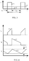
- FIG. 3 shows the timing of activating the high-side switch 12 and the low-side switch 18 of FIG. 1 and FIG. 2 .
- the high-side switch 12 is on and the low-side switch 18 is off, corresponding to the ON configuration shown in FIG. 1 .
- the timing pulse 52 the high-side switch 12 is off and the low-side switch 18 is on, corresponding to the OFF configuration shown in FIG. 2 . Consequently, an output voltage 54 is formed across the load capacitor 28.
- FIG. 4 shows the currents of FIG. 1 and FIG. 2 in relation to the switch timing of FIG. 3 .
- the high-side switch 12 is closed and current 32 (I A ) flows, causing an increase in the load current 34 (I L ).
- the low-side switch 18 is closed and current 42 (I B ) flows, causing a decrease in the load current 34 (I L ).
- the two currents 32 and 42 flowing in an interleaved fashion form the load current 34 shown as a saw tooth pattern with a current range 60.
- the current range 60 is smoothed (e.g., filtered) by the load capacitor 28, thereby producing the output voltage 54.
- an embodiment 70 includes a high-side transistor (e.g., a power FET) 72 having a drain connected to a voltage supply 74 and a source connected to a phase node 76.
- a low-side transistor (e.g., a power FET) 78 has a drain connected to the phase node 76 and a source connected to a ground 80.
- a switch controller 90 communicates with a driver 92 over a connection 94, in response to a PWM signal 96.
- the switch control 90 signals the driver 92 to activate a gate 100 of the high-side transistor 72 during a first timing phase, and to activate a gate 102 of the low-side transistor 78 during a second timing phase.
- the first timing phase and the second timing phase are non-overlapping.
- the first timing phase and the second timing phase are the timing pulse 50 and the timing pulse 52 as shown in FIG. 3 .
- the phase node 76 connects a load capacitor through a load inductor as shown in FIG. 1 and FIG. 2 and supplies a load current 104.
- the high-side transistor 72 and the low-side transistor 78 have the same temperature coefficient and are driven by the same gate voltage during their respective timing phases. Specifically, the resistance between the respective drain and source, including the active channel and junction resistance, changes with respect to temperature at the same rate for both the high-side transistor 72 and the low-side transistor 78, and both transistors are of the same dopant type (e.g. N-channel FET). A current flowing through either the high-side transistor 72 or the low-side transistor 78 develops a respective transistor voltage across the respective resistance and is sensed with a respective current sense channel 110a or 110b.
- the resistance between the respective drain and source including the active channel and junction resistance
- the resistance between the respective drain and source changes with respect to temperature at the same rate for both the high-side transistor 72 and the low-side transistor 78, and both transistors are of the same dopant type (e.g. N-channel FET).
- a current flowing through either the high-side transistor 72 or the low-side transistor 78 develops a respective transistor voltage across
- the current sense channel 110a includes a transconductance amplifier 112a configured to sense the transistor voltage between the drain and source terminals of the high-side transistor 72 to generate an amplifier output current 114a on a node 116a.
- the transconductance amplifier 112a is active only when the high-side transistor 72 is active by activating the gate 100. Gating the activation of the transconductance amplifier 112a prevents saturation of this amplifier because the transistor voltage across the high-side transistor 72 will increase significantly when the high-side transistor 72 is deactivated.
- the amplifier output current 114a is adjusted by a Multiplying Digital to Analog Converter (Multiplying DAC or MDAC) 118a to generate a first calibration current 120a on the first calibration node 122a.
- Multiplying DAC or MDAC Multiplying Digital to Analog Converter
- the first calibration current 120a is sunk by a first calibration resistor 124a connected between the first calibration node 122a and the ground 80. Accordingly, a first calibration voltage is generated across the first calibration resistor 124a.
- the MDAC 118a adjusts the amplifier output current 114a by a gain determined by a gain coefficient 126 to produce the first calibration current 120a, hence the MDAC 118a is also referred to as a Current DAC or IDAC.
- the current sense channel 110b includes a transconductance amplifier 112b configured to sense the transistor voltage between the drain and source terminals of the low-side transistor 78 to generate an amplifier output current 114b on a node 116b.
- the transconductance amplifier 112b is active only when the low-side transistor 78 is active by activating the gate 102. Gating the activation of the transconductance amplifier 112b prevents saturation of this amplifier because the transistor voltage across the low-side transistor 78 will increase significantly when the high-side transistor 72 is deactivated.
- the amplifier output current 114b is adjusted by an MDAC 118b to generate a second calibration current 120b on the second calibration node 122b.
- the second calibration current 120b is sunk by a second calibration resistor 124b connected between the second calibration node 122b and the ground 80. Accordingly, a second calibration voltage is generated across the second calibration resistor 124b.
- the MDAC 118b adjusts the amplifier output current 114b by a gain determined by the gain coefficient 126 to produce the second calibration current 120b, hence the MDAC 118b is also referred to as a Current DAC or IDAC.
- the respective calibration voltages on the calibration nodes 122a and 122b are alternately connected with respective switches 130 and 132 controlled by respective control signals 134 and 136 to generate an output voltage 140.
- the control signals 124 and 136 are synchronized to the activation of the respective high-side transistor 72 and the low-side transistor 78.
- the high-side transistor 72, the transconductance amplifier 112a and the switch 130 are activated during a first time period.
- the low-side transistor 78, the transconductance amplifier 112b and the switch 132 are activated during a second time period, wherein the first time period and the second time period are interleaved and non-overlapping.
- an additional controller uses the output voltage 140 to control and generate the PWM signal 96.
- the output voltage 140 is used for monitoring over-voltage protection of a switching converter including the current sense system 70.
- a transistor gain of the high-side transistor 72 and low-side transistor 78 are designed to be the same through proper layout techniques.
- the term "transistor gain" refers to a channel width of a transistor divided by a channel length of the transistor.
- a difference in the transistor gain between the high-side transistor 72 and low-side transistor 78 is compensated by either adjusting a gain of the MDAC 118a relative to the MDAC 118b or by adjusting a resistance of the calibration resistor 124a relative to the resistance of the calibration resistor 124b, or both.
- the high-side transistor 72 and low-side transistor 78 are placed (e.g. "laid out") in close proximity to each other.
- the calibration resistors 124a and 124b have matched resistance.
- the calibration resistors 124a and 124b are designed to be in close proximity to one another including usage of common-centroid layout practices and the like.
- FIG. 6 shows an embodiment 150 of a calibration circuit used to normalize the temperature dependency of the high-side transistor 72 and the low-side transistor 78 of FIG. 5 .
- the embodiment 150 includes a reference transistor 152 having a drain 154, a source connected to a ground 156, and a gate 158.
- the gate 158 is continuously biased to a same value as the pulsed gate values generated by the driver 92 of FIG. 5 , applied to the gates 100 and 102.
- the drain 154 is connected to a Zero Temperature Coefficient (ZTC) current source 160 supplied by a voltage source 162.
- ZTC Zero Temperature Coefficient
- the voltage source 162 is pulsed to enable current conduction through the reference transistor 152 only when calibration of the embodiment 70 of FIG. 5 is required.
- calibration occurs continuously to achieve the most accurate temperature compensation of the embodiment 70.
- calibration occurs infrequently when operating voltage and temperatures are relatively stable, and previously latched calibration values are used.
- a temperature and/or voltage monitor is used to trigger an update of calibration values when the temperature and/or voltage changes by a respective threshold value.
- the transistor gain for the reference transistor 152 is less than the transistor gain of either the high-side transistor 72 or the low-side transistor 78 of FIG. 5 , thereby reducing power consumption. Similar to the compensation methods described for transistor gain imbalances between the high-side transistor 72 and the low-side transistor 78, the reduced gain of the reference transistor 152 is compensated by adjusting a gain of both of the MDACs 118a and 188b by the same amount, or by adjusting the resistance of both of the calibration resistors 124a and 124b, or by adjusting both the MDACs and calibration resistors in proportional amounts.
- the reference transistor 152 is placed in close proximity to the high-side transistor 72 and the low-side transistor 78 (e.g. "laid out”).
- a calibration resistor 184 of the embodiment 150 has a matched resistance to the calibration resistors 124a and 124b.
- the calibration resistors 184, 124a and 124b are designed to be in close proximity to one another including usage of common-centroid layout practices and the like.
- the embodiment 150 includes a current sense channel 170 configured to sense a transistor voltage between the drain and source of the reference transistor 152 and to generate a calibration voltage on the calibration node 182.
- the current sense channel 170 includes a transconductance amplifier 172 connected between the drain and source of the reference transistor 152 and configured to sense a transistor voltage therebetween and to generate an amplifier output current 174 on a node 176.
- An MDAC 178 (also referred to as IDAC) receives the amplifier output current 174 and generates a calibration current 180 multiplied by a gain determined by the gain coefficient 186.
- the calibration voltage is formed on the calibration node 182 by a calibration resistor 184 connected to the ground 186 and configured to sink the calibration current 180.
- each of the calibration resistors 124a, 124b and 184 have a nominal resistance of 60 kilohms.
- the calibration voltage on the calibration node 182 is compared against a target voltage 190 with a low offset comparator 192 to generate an error voltage 194.
- the error voltage 194 is converted by an Analog to Digital Converter (ADC) 196 to determine the gain coefficient 186.
- ADC Analog to Digital Converter
- the ADC 196 is a sampling ADC.
- the gain coefficient 186 has a data width of six bits. The resolution of the calibration is related to the number of bits of the gain coefficient 186.
- the target voltage 190 is determined by converting a target coefficient 202 with a DAC 204.
- the target coefficient 202 is determined by measuring a calibration voltage of one of the current sense channels 110a or 110b corresponding to a gate bias on the respective gate 100 or 102, for a targeted load current 104 flowing flow an inductor (not shown), and for a targeted operating temperature, wherein the inductor is connected between the phase node 76 and a load capacitor (not shown).
- the target coefficient is determined to replicate the measured calibration voltage as the target voltage 190.
- the target coefficient 202 is stored in a One Time Programmable memory, a set of polysilicon or metal fuses, an EPROM, an EEPROM or the like. In one embodiment, the target coefficient 202 is determined at a final package test. In another embodiment, the target coefficient 202 is determined at a wafer probe test. In one embodiment, the gain coefficient 186 generated by the ADC 196 is supplied directly to the MDACs 118a and 118b. In another embodiment, the gain coefficient 186 is averaged over a plurality of clock samples of the ADC 196 and stored in a latch 198 to provide an averaged gain coefficient 200 to the MDACs 118a and 118b as the gain coefficient 126, shown in FIG. 5 .
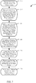
- FIG. 7 shows a method 210 for dynamic calibration of current sense for switching converters according to an example embodiment of the present disclosure.
- a reference transistor 152 is biased with a ZTC current source 160.
- a gate 158 of the reference transistor 152 and a power transistor 72 (or 78) is biased with a gate voltage, wherein each transistor has a same temperature coefficient.
- a transistor voltage sensed across the reference transistor 152 is multiplied by a gain to generate a first calibration voltage, wherein the gain is determined by a gain coefficient 186.
- a transistor voltage sensed across the power transistor 72 (or 78) is multiplied by the gain to generate a second calibration voltage.
- the first calibration voltage formed from the reference transistor 152, is compared to a target voltage 190 to generate an error voltage 194.
- the gain coefficient 186 is determined with an ADC 196 in response to the error voltage 194.
- a difference between the target voltage 190 and each of the calibration voltages is minimized.
- the dynamic calibration of current sense disclosed herein provides for high-speed and stable sensing because the current sense channels 110a and 110b are in an open loop configuration. Furthermore, the calibration is largely independent of the PWM duty cycle, supply voltage changes and the load inductor value. The temperature calibration consumes very little current and operates over a variety of environments with varying degrees of temperature, voltage and process variation.
- a system for dynamic calibration of current sense for switching converters comprises a first one, a second one and a third one of a plurality of current sense channels configured to multiply a respective transistor voltage sensed across a respective transistor by a gain to generate a respective calibration voltage across a respective resistor, wherein the gain is determined by a gain coefficient, and each respective transistor has a matching temperature coefficient and a respective gate.
- the respective transistor of the first one of the current sense channels is connected between a voltage supply and a phase node.
- the respective calibration resistor is connected to an output by a respective switch during a first phase.
- the respective gate is biased to a first voltage during the first phase.
- the respective transistor of the second one of the current sense channels is connected between the phase node and a ground.
- the respective calibration resistor is connected to the output by a respective switch during a second phase not overlapping in time with the first phase.
- the respective gate is biased to the first voltage during the second phase.
- the respective transistor of the third one of the current sense channels is connected between a Zero Temperature Coefficient (ZTC) current source and the ground.
- the respective gate is biased to the first voltage.
- a comparator is configured to compare the respective calibration voltage of the third sense channel to a target voltage to generate an error voltage.
- An Analog to Digital Converter is configured to convert the error voltage into the gain coefficient, thereby minimizing the error voltage and a difference between the target voltage and each respective calibration voltage.
- a method for dynamic calibration of current sense for switching converters comprises biasing a reference transistor with a Zero Temperature Coefficient (ZTC) current source, and a respective gate of each of the reference transistor and a power transistor with a gate voltage, wherein each of the reference transistor and the power transistor comprise a matching temperature coefficient.
- ZTC Zero Temperature Coefficient
- a reference voltage sensed across the reference transistor is multiplied by a first gain, thereby generating a first calibration voltage, wherein the first gain is determined by a gain coefficient.
- a transistor voltage sensed across the power transistor is multiplied by the first gain, thereby generating a second calibration voltage.
- the first calibration voltage is compared to a target voltage to generate an error voltage.
- the gain coefficient is determined with an Analog to Digital Converter in response to the error voltage, thereby minimizing the error voltage and a difference between the target voltage and each of the first calibration voltage and the second calibration voltage.
- an apparatus for dynamic calibration of current sense for switching converters comprises a first one of a plurality of current sense is channels configured to multiply by a first gain, a first voltage sensed between a first drain and a first source of a first transistor, and to generate a first calibration voltage therefrom, wherein the first gain is defined by a gain coefficient, and wherein a first gate voltage on a first gate of the first transistor controls a first current flowing between the first drain and the first source.
- a second one of the plurality of current sense channels is configured to multiply by the first gain, a second voltage sensed between a second drain and a second source of a second transistor, and to generate a second calibration voltage therefrom.
- the second drain is connected to a Zero Temperature Coefficient (ZTC) current source.
- ZTC Zero Temperature Coefficient
- the second source is connected to a ground.
- a second gate of the second transistor is biased to the first gate voltage and a first temperature coefficient of the first transistor is equal to a second temperature coefficient of the second transistor.
- a comparator is configured to generate an error voltage from a difference between the second calibration voltage and a target voltage.
- An Analog to Digital Converter is configured to determine the gain coefficient proportional to the error voltage, thereby minimizing the error voltage and a difference between the target voltage and each of the first calibration voltage and the second calibration voltage.
Landscapes
- Physics & Mathematics (AREA)
- General Physics & Mathematics (AREA)
- Engineering & Computer Science (AREA)
- Power Engineering (AREA)
- Dc-Dc Converters (AREA)
Abstract
Description
- This disclosure relates generally to temperature compensation, and more specifically to temperature compensation of an output stage of a Pulse Width Modulated (PWM) power converter.
- Switching converters typically convert a variable input voltage to supply a regulated power output over a wide temperature range. Regulation of the supplied power may include monitoring output current and/or voltage characteristics to regulate a switching frequency of a PWM stage designed to switch power Field Effect Transistors (FETs). For proper power regulation, the temperature dependence of the power FETs requires compensation.
- Existing temperature compensation techniques include the use of external components, which adds considerable cost and often additional connections or component level pins for the converter. Power converter efficiency is also an important design goal, hence lossless methods of temperature compensation are usually preferred. However, techniques to sense and compensate for FET temperature characteristics have been relatively slow and consume a lot of power.
- Other techniques based on sense FET topologies can give good performance at lower switching frequencies but have limited bandwidth and become too limited for use at higher switching frequencies (e.g., above 2 MHz). Depending on the ratio used, the sense current using this technique can reduce the system efficiency at lighter loads.
- Aspects of the disclosure are defined in the accompanying claims.
- In a first aspect, there is provided a system for dynamic calibration of current sense for switching converters comprising:
- a first one, a second one and a third one of a plurality of current sense channels configured to multiply a respective transistor voltage sensed across a respective transistor by a gain to generate a respective calibration voltage across a respective resistor, wherein the gain is determined by a gain coefficient, and each respective transistor has a matching temperature coefficient and a respective gate,
- the respective transistor of the first one of the current sense channels connected between a voltage supply and a phase node, the respective calibration resistor connected to an output by a respective switch during a first phase, and the respective gate biased to a first voltage during the first phase,
- the respective transistor of the second one of the current sense channels connected between the phase node and a ground, the respective calibration resistor connected to the output by a respective switch during a second phase not overlapping in time with the first phase, and the respective gate biased to the first voltage during the second phase,
- the respective transistor of the third one of the current sense channels connected between a Zero Temperature Coefficient (ZTC) current source and the ground, and the respective gate biased to the first voltage;
- a comparator configured to compare the respective calibration voltage of the third sense channel to a target voltage to generate an error voltage; and
- an Analog to Digital Converter configured to convert the error voltage into the gain coefficient, thereby minimizing the error voltage and a difference between the target voltage and each respective calibration voltage.
- In one or more embodiments, each of the current sense channels may comprise a transconductance amplifier configured to sense the respective transistor voltage, a Multiplying Digital to Analog Converter configured to multiply an amplifier output current of the transconductance amplifier by the gain to provide a calibration current, and the calibration resistor configured to sink the calibration current to generate the calibration voltage.
- In one or more embodiments, a latch may be configured to store an averaged gain coefficient of a plurality of samples of the gain coefficient, and the gain of the first one and the second one of the current sense channels is determined by the averaged gain coefficient.
- In one or more embodiments, the system may further comprise a load inductor connected between the phase node and a load capacitor, wherein a regulated voltage of the switching converter is formed on the load capacitor.
- In one or more embodiments, the target voltage may be determined by measuring a respective calibration voltage of the third one of the current sense channels corresponding the respective transistor biased to the first voltage and an average target current flowing though the load inductor.
- In one or more embodiments, the gain coefficient is determined while the ZTC current source is activated with a pulsed source.
- In a second aspect, there is provided a method for dynamic calibration of current sense for switching converters comprising: biasing a reference transistor with a Zero Temperature Coefficient (ZTC) current source, and a respective gate of each of the reference transistor and a power transistor with a gate voltage, wherein each of the reference transistor and the power transistor comprises a matching temperature coefficient; multiplying a reference voltage sensed across the reference transistor by a first gain, thereby generating a first calibration voltage, wherein the first gain is determined by a gain coefficient; multiplying a transistor voltage sensed across the power transistor by the first gain, thereby generating a second calibration voltage; comparing the first calibration voltage to a target voltage to generate an error voltage; and determining the gain coefficient with an Analog to Digital Converter in response to the error voltage, thereby minimizing the error voltage and a difference between the target voltage and each of the first calibration voltage and the second calibration voltage.
- In one or more embodiments, the method may further comprise activating the ZTC current source with a pulsed current source, wherein the gain coefficient is determined while the ZTC current source is activated.
- In one or more embodiments, generating the first calibration voltage may further comprise sensing the reference voltage with a transconductance amplifier, converting an amplifier output of the transconductance amplifier with a Multiplying Digital to Analog Converter (MDAC) controlled by the first gain and generating the first calibration voltage by sinking an calibration current generated by the MDAC through a calibration resistor.
- In one or more embodiments, the method may further comprise compensating for a difference in a transistor gain between the reference transistor and the power transistor by changing a second gain of the MDAC.
- In one or more embodiments, the method may further comprise compensating for a difference in a transistor gain between the reference transistor and the power transistor by changing a first resistance value of the calibration resistor used to determine the first calibration voltage relative to a second resistance value of a second calibration resistor used to determine the second calibration voltage.
- In one or more embodiments, the method may further comprise deactivating the transconductance amplifier in response to deactivating the power transistor.
- In one or more embodiments, the method may further comprise determining the target voltage by measuring the first calibration voltage corresponding to the reference transistor biased by the gate voltage and an average target current flowing through a load inductor connected between a load capacitor and the power transistor.
- In a third aspect, there is provided an apparatus for dynamic calibration of current sense for switching converters comprising: a first one of a plurality of current sense channels configured to multiply by a first gain, a first voltage sensed between a first drain and a first source of a first transistor, and to generate a first calibration voltage therefrom, wherein the first gain is defined by a gain coefficient, and wherein a first gate voltage on a first gate of the first transistor controls a first current flowing between the first drain and the first source; a second one of the plurality of current sense channels configured to multiply by the first gain, a second voltage sensed between a second drain and a second source of a second transistor, and to generate a second calibration voltage therefrom, the second drain connected to a Zero Temperature Coefficient (ZTC) current source, the second source connected to a ground, a second gate of the second transistor biased to the first gate voltage and a first temperature coefficient of the first transistor equal to a second temperature coefficient of the second transistor; a comparator configured to generate an error voltage from a difference between the second calibration voltage and a target voltage; and an Analog to Digital Converter configured to determine the gain coefficient proportional to the error voltage, thereby minimizing the error voltage and a difference between the target voltage and each of the first calibration voltage and the second calibration voltage.
- In one or more embodiments, each of the current sense channels may comprise a respective transconductance amplifier configured to sense a respective voltage between a respective drain and a respective source of the respective transistor, a respective Multiplying Digital to Analog Converter configured to multiply a respective amplifier output current of the respective transconductance amplifier by the first gain to provide a respective calibration current, and a respective calibration resistor configured to sink the respective calibration current to generate the respective calibration voltage.
- In one or more embodiments, each of the respective calibration resistors of the current sense channels may have a same resistance.
- In one or more embodiments, a first transistor gain of the first transistor may be greater than a second transistor gain of the second transistor, thereby reducing a second transistor current.
- In one or more embodiments, a difference between the first transistor gain and the second transistor gain is compensated by a proportional change in a second gain of a respective Multiplying Digital to Analog Converter (MDAC) of the first one of the plurality of current sense channels, wherein the respective MDAC is configured to multiply the first voltage by the first gain to generate the first calibration voltage.
- In one or more embodiments, a difference between the first transistor gain and the second transistor gain may be compensated by a proportional change in a resistance of a respective resistor of the first one of the plurality of current sense channels, wherein the respective resistor may be configured to generate the first calibration voltage from a first calibration current.
- In one or more embodiments, the apparatus may further comprise a switch configured to periodically activate the ZTC current source while the gain coefficient is determined.
- The present invention is illustrated by way of example and is not limited by the accompanying figures, in which like references indicate similar elements. Elements in the figures are illustrated for simplicity and clarity and have not necessarily been drawn to scale.
-
FIG. 1 is a schematic view of an embodiment of an output driver of a Pulse Width Modulated (PWM) power converter in an ON state. -
FIG. 2 is a schematic view of an embodiment of an output driver of a PWM power converter in an OFF state. -
FIG. 3 is a graphical view of timing waveforms of the embodiments ofFIG. 1 and FIG. 2 showing switch activation. -
FIG. 4 is a graphical view of timing waveforms of the embodiments ofFIG. 1 and FIG. 2 showing output current. -
FIG. 5 is a schematic view of a current sense system in accordance with an example embodiment of the present disclosure. -
FIG. 6 is a schematic view of a calibration circuit in accordance with an example embodiment of the present disclosure. -
FIG. 7 is a flowchart representation of a method for dynamic calibration of current sense for switching converters in accordance with an example embodiment of the present disclosure. - Embodiments described herein provide for lossless compensation of FET current variance due to temperature dependencies, fabrication process variation and input voltage changes. A separate calibration FET is used outside of the switching converter's inner control loop resulting in high-speed and accurate compensation. The calibration FET is biased with a Zero Temperature Coefficient (ZTC) current source to detect temperature variations and is used to adjust the gain of amplifiers used in the inner control loop of the switching converter. Specifically, the ZTC current source, as referred to throughout this disclosure, has a temperature coefficient significantly lower than a respective temperature coefficient of the transistor biased by the ZTC current source. Accordingly, temperature variations of the ZTC current source are insignificant compared to the temperature variations of the transistor being calibrated.
-
FIG. 1 shows anembodiment 10 of an output stage of a buck PWM converter. A high-side switch 12 is connected between avoltage supply node 14 and aphase node 16. A low-side switch 18 is connected between thephase node 16 and aground 20. Thevoltage supply node 14 includes avoltage supply 22 connect toground 20. Thephase node 16 is connected to aload inductor 26. Theload inductor 26 connects to aload capacitor 28 connected toground 20 and aload resistor 30 connected toground 20. Theembodiment 10 shows a PWM converter in the ON configuration, wherein the high-side switch 12 is closed, the low-side switch 18 is open, and a current 32 flows from thevoltage supply 22 through theload inductor 26, thereby producing aload current 34. -
FIG. 2 shows anembodiment 40, similar to theembodiment 10 ofFIG. 1 , in an OFF configuration. InFIG. 2 , the high-side switch 12 is open, the low-side switch 18 is closed, and a current 42 flows from theground 20 through theload inductor 26, thereby producing theload current 34.FIG. 3 shows the timing of activating the high-side switch 12 and the low-side switch 18 ofFIG. 1 and FIG. 2 . During thetime pulse 50, the high-side switch 12 is on and the low-side switch 18 is off, corresponding to the ON configuration shown inFIG. 1 . During thetiming pulse 52, the high-side switch 12 is off and the low-side switch 18 is on, corresponding to the OFF configuration shown inFIG. 2 . Consequently, anoutput voltage 54 is formed across theload capacitor 28. -
FIG. 4 shows the currents ofFIG. 1 and FIG. 2 in relation to the switch timing ofFIG. 3 . Specifically, during thetiming pulse 50, the high-side switch 12 is closed and current 32 (IA) flows, causing an increase in the load current 34 (IL). During thetiming pulse 52, the low-side switch 18 is closed and current 42 (IB) flows, causing a decrease in the load current 34 (IL). The twocurrents current range 60. Thecurrent range 60 is smoothed (e.g., filtered) by theload capacitor 28, thereby producing theoutput voltage 54. - Turning now to
FIG. 5 andFIG. 6 , example embodiments of a current sense system in accordance with the present disclosure are described. InFIG. 5 , anembodiment 70 includes a high-side transistor (e.g., a power FET) 72 having a drain connected to avoltage supply 74 and a source connected to aphase node 76. A low-side transistor (e.g., a power FET) 78 has a drain connected to thephase node 76 and a source connected to aground 80. Aswitch controller 90 communicates with adriver 92 over aconnection 94, in response to aPWM signal 96. Specifically, theswitch control 90 signals thedriver 92 to activate agate 100 of the high-side transistor 72 during a first timing phase, and to activate agate 102 of the low-side transistor 78 during a second timing phase. The first timing phase and the second timing phase are non-overlapping. In one embodiment, the first timing phase and the second timing phase are the timingpulse 50 and thetiming pulse 52 as shown inFIG. 3 . In an example embodiment, thephase node 76 connects a load capacitor through a load inductor as shown inFIG. 1 and FIG. 2 and supplies a load current 104. - In an example embodiment, the high-
side transistor 72 and the low-side transistor 78 have the same temperature coefficient and are driven by the same gate voltage during their respective timing phases. Specifically, the resistance between the respective drain and source, including the active channel and junction resistance, changes with respect to temperature at the same rate for both the high-side transistor 72 and the low-side transistor 78, and both transistors are of the same dopant type (e.g. N-channel FET). A current flowing through either the high-side transistor 72 or the low-side transistor 78 develops a respective transistor voltage across the respective resistance and is sensed with a respectivecurrent sense channel - The
current sense channel 110a includes atransconductance amplifier 112a configured to sense the transistor voltage between the drain and source terminals of the high-side transistor 72 to generate an amplifier output current 114a on anode 116a. In an example embodiment, thetransconductance amplifier 112a is active only when the high-side transistor 72 is active by activating thegate 100. Gating the activation of thetransconductance amplifier 112a prevents saturation of this amplifier because the transistor voltage across the high-side transistor 72 will increase significantly when the high-side transistor 72 is deactivated. The amplifier output current 114a is adjusted by a Multiplying Digital to Analog Converter (Multiplying DAC or MDAC) 118a to generate a first calibration current 120a on thefirst calibration node 122a. The first calibration current 120a is sunk by afirst calibration resistor 124a connected between thefirst calibration node 122a and theground 80. Accordingly, a first calibration voltage is generated across thefirst calibration resistor 124a. TheMDAC 118a adjusts theamplifier output current 114a by a gain determined by again coefficient 126 to produce the first calibration current 120a, hence theMDAC 118a is also referred to as a Current DAC or IDAC. - The
current sense channel 110b includes atransconductance amplifier 112b configured to sense the transistor voltage between the drain and source terminals of the low-side transistor 78 to generate an amplifier output current 114b on anode 116b. In an example embodiment, thetransconductance amplifier 112b is active only when the low-side transistor 78 is active by activating thegate 102. Gating the activation of thetransconductance amplifier 112b prevents saturation of this amplifier because the transistor voltage across the low-side transistor 78 will increase significantly when the high-side transistor 72 is deactivated. The amplifier output current 114b is adjusted by anMDAC 118b to generate a second calibration current 120b on thesecond calibration node 122b. The second calibration current 120b is sunk by asecond calibration resistor 124b connected between thesecond calibration node 122b and theground 80. Accordingly, a second calibration voltage is generated across thesecond calibration resistor 124b. TheMDAC 118b adjusts the amplifier output current 114b by a gain determined by thegain coefficient 126 to produce the second calibration current 120b, hence theMDAC 118b is also referred to as a Current DAC or IDAC. - The respective calibration voltages on the
calibration nodes respective switches respective control signals output voltage 140. The control signals 124 and 136 are synchronized to the activation of the respective high-side transistor 72 and the low-side transistor 78. In an example embodiment, the high-side transistor 72, thetransconductance amplifier 112a and theswitch 130 are activated during a first time period. Similarly, the low-side transistor 78, thetransconductance amplifier 112b and theswitch 132 are activated during a second time period, wherein the first time period and the second time period are interleaved and non-overlapping. - In an example embodiment, an additional controller uses the
output voltage 140 to control and generate thePWM signal 96. In another example embodiment, theoutput voltage 140 is used for monitoring over-voltage protection of a switching converter including thecurrent sense system 70. In addition to the high-side transistor 72 and low-side transistor 78 having a same temperature coefficient and gate drive voltage, in an example embodiment a transistor gain of the high-side transistor 72 and low-side transistor 78 are designed to be the same through proper layout techniques. The term "transistor gain" refers to a channel width of a transistor divided by a channel length of the transistor. - In another example embodiment, a difference in the transistor gain between the high-
side transistor 72 and low-side transistor 78 is compensated by either adjusting a gain of theMDAC 118a relative to theMDAC 118b or by adjusting a resistance of thecalibration resistor 124a relative to the resistance of thecalibration resistor 124b, or both. In one embodiment, the high-side transistor 72 and low-side transistor 78 are placed (e.g. "laid out") in close proximity to each other. In another example embodiment, thecalibration resistors calibration resistors -
FIG. 6 shows anembodiment 150 of a calibration circuit used to normalize the temperature dependency of the high-side transistor 72 and the low-side transistor 78 ofFIG. 5 . Theembodiment 150 includes areference transistor 152 having adrain 154, a source connected to aground 156, and agate 158. Thegate 158 is continuously biased to a same value as the pulsed gate values generated by thedriver 92 ofFIG. 5 , applied to thegates drain 154 is connected to a Zero Temperature Coefficient (ZTC)current source 160 supplied by avoltage source 162. In an example embodiment, thevoltage source 162 is pulsed to enable current conduction through thereference transistor 152 only when calibration of theembodiment 70 ofFIG. 5 is required. - In one example embodiment, calibration occurs continuously to achieve the most accurate temperature compensation of the
embodiment 70. In another example, calibration occurs infrequently when operating voltage and temperatures are relatively stable, and previously latched calibration values are used. In another embodiment, a temperature and/or voltage monitor is used to trigger an update of calibration values when the temperature and/or voltage changes by a respective threshold value. - In another example embodiment, the transistor gain for the
reference transistor 152 is less than the transistor gain of either the high-side transistor 72 or the low-side transistor 78 ofFIG. 5 , thereby reducing power consumption. Similar to the compensation methods described for transistor gain imbalances between the high-side transistor 72 and the low-side transistor 78, the reduced gain of thereference transistor 152 is compensated by adjusting a gain of both of theMDACs 118a and 188b by the same amount, or by adjusting the resistance of both of thecalibration resistors - In one embodiment, the
reference transistor 152 is placed in close proximity to the high-side transistor 72 and the low-side transistor 78 (e.g. "laid out"). In another example embodiment, acalibration resistor 184 of theembodiment 150 has a matched resistance to thecalibration resistors calibration resistors - The
embodiment 150 includes acurrent sense channel 170 configured to sense a transistor voltage between the drain and source of thereference transistor 152 and to generate a calibration voltage on thecalibration node 182. Thecurrent sense channel 170 includes atransconductance amplifier 172 connected between the drain and source of thereference transistor 152 and configured to sense a transistor voltage therebetween and to generate an amplifier output current 174 on anode 176. An MDAC 178 (also referred to as IDAC) receives the amplifier output current 174 and generates a calibration current 180 multiplied by a gain determined by thegain coefficient 186. The calibration voltage is formed on thecalibration node 182 by acalibration resistor 184 connected to theground 186 and configured to sink thecalibration current 180. In an example embodiment, each of thecalibration resistors - The calibration voltage on the
calibration node 182 is compared against atarget voltage 190 with a low offsetcomparator 192 to generate anerror voltage 194. Theerror voltage 194 is converted by an Analog to Digital Converter (ADC) 196 to determine thegain coefficient 186. In an example embodiment, theADC 196 is a sampling ADC. In another embodiment, thegain coefficient 186 has a data width of six bits. The resolution of the calibration is related to the number of bits of thegain coefficient 186. Thetarget voltage 190 is determined by converting atarget coefficient 202 with aDAC 204. With reference toFIG. 5 along withFIG. 6 , in one embodiment, thetarget coefficient 202 is determined by measuring a calibration voltage of one of thecurrent sense channels respective gate phase node 76 and a load capacitor (not shown). The target coefficient is determined to replicate the measured calibration voltage as thetarget voltage 190. - In an example embodiment, the
target coefficient 202 is stored in a One Time Programmable memory, a set of polysilicon or metal fuses, an EPROM, an EEPROM or the like. In one embodiment, thetarget coefficient 202 is determined at a final package test. In another embodiment, thetarget coefficient 202 is determined at a wafer probe test. In one embodiment, thegain coefficient 186 generated by theADC 196 is supplied directly to theMDACs gain coefficient 186 is averaged over a plurality of clock samples of theADC 196 and stored in alatch 198 to provide an averagedgain coefficient 200 to theMDACs gain coefficient 126, shown inFIG. 5 . - Referring to
FIGs. 5-7 ,FIG. 7 shows amethod 210 for dynamic calibration of current sense for switching converters according to an example embodiment of the present disclosure. At 212, areference transistor 152 is biased with a ZTCcurrent source 160. At 214, agate 158 of thereference transistor 152 and a power transistor 72 (or 78) is biased with a gate voltage, wherein each transistor has a same temperature coefficient. At 216, a transistor voltage sensed across thereference transistor 152 is multiplied by a gain to generate a first calibration voltage, wherein the gain is determined by again coefficient 186. At 218, a transistor voltage sensed across the power transistor 72 (or 78) is multiplied by the gain to generate a second calibration voltage. At 220, the first calibration voltage, formed from thereference transistor 152, is compared to atarget voltage 190 to generate anerror voltage 194. At 222, thegain coefficient 186 is determined with anADC 196 in response to theerror voltage 194. At 224, a difference between thetarget voltage 190 and each of the calibration voltages is minimized. - The dynamic calibration of current sense disclosed herein, provides for high-speed and stable sensing because the
current sense channels - As will be appreciated, embodiments as disclosed include at least the following. In one embodiment, a system for dynamic calibration of current sense for switching converters comprises a first one, a second one and a third one of a plurality of current sense channels configured to multiply a respective transistor voltage sensed across a respective transistor by a gain to generate a respective calibration voltage across a respective resistor, wherein the gain is determined by a gain coefficient, and each respective transistor has a matching temperature coefficient and a respective gate. The respective transistor of the first one of the current sense channels is connected between a voltage supply and a phase node. The respective calibration resistor is connected to an output by a respective switch during a first phase. The respective gate is biased to a first voltage during the first phase. The respective transistor of the second one of the current sense channels is connected between the phase node and a ground. The respective calibration resistor is connected to the output by a respective switch during a second phase not overlapping in time with the first phase. The respective gate is biased to the first voltage during the second phase. The respective transistor of the third one of the current sense channels is connected between a Zero Temperature Coefficient (ZTC) current source and the ground. The respective gate is biased to the first voltage. A comparator is configured to compare the respective calibration voltage of the third sense channel to a target voltage to generate an error voltage. An Analog to Digital Converter is configured to convert the error voltage into the gain coefficient, thereby minimizing the error voltage and a difference between the target voltage and each respective calibration voltage.
- In another embodiment, a method for dynamic calibration of current sense for switching converters comprises biasing a reference transistor with a Zero Temperature Coefficient (ZTC) current source, and a respective gate of each of the reference transistor and a power transistor with a gate voltage, wherein each of the reference transistor and the power transistor comprise a matching temperature coefficient. A reference voltage sensed across the reference transistor is multiplied by a first gain, thereby generating a first calibration voltage, wherein the first gain is determined by a gain coefficient. A transistor voltage sensed across the power transistor is multiplied by the first gain, thereby generating a second calibration voltage. The first calibration voltage is compared to a target voltage to generate an error voltage. The gain coefficient is determined with an Analog to Digital Converter in response to the error voltage, thereby minimizing the error voltage and a difference between the target voltage and each of the first calibration voltage and the second calibration voltage.
- In another embodiment, an apparatus for dynamic calibration of current sense for switching converters comprises a first one of a plurality of current sense is channels configured to multiply by a first gain, a first voltage sensed between a first drain and a first source of a first transistor, and to generate a first calibration voltage therefrom, wherein the first gain is defined by a gain coefficient, and wherein a first gate voltage on a first gate of the first transistor controls a first current flowing between the first drain and the first source. A second one of the plurality of current sense channels is configured to multiply by the first gain, a second voltage sensed between a second drain and a second source of a second transistor, and to generate a second calibration voltage therefrom. The second drain is connected to a Zero Temperature Coefficient (ZTC) current source. The second source is connected to a ground. A second gate of the second transistor is biased to the first gate voltage and a first temperature coefficient of the first transistor is equal to a second temperature coefficient of the second transistor. A comparator is configured to generate an error voltage from a difference between the second calibration voltage and a target voltage. An Analog to Digital Converter is configured to determine the gain coefficient proportional to the error voltage, thereby minimizing the error voltage and a difference between the target voltage and each of the first calibration voltage and the second calibration voltage.
- Although the invention is described herein with reference to specific embodiments, various modifications and changes can be made without departing from the scope of the present invention as set forth in the claims below. Accordingly, the specification and figures are to be regarded in an illustrative rather than a restrictive sense, and all such modifications are intended to be included within the scope of the present invention. Any benefits, advantages, or solutions to problems that are described herein with regard to specific embodiments are not intended to be construed as a critical, required, or essential feature or element of any or all the claims.
- Unless stated otherwise, terms such as "first" and "second" are used to arbitrarily distinguish between the elements such terms describe. Thus, these terms are not necessarily intended to indicate temporal or other prioritization of such elements.
Claims (13)
- A system for dynamic calibration of current sense for switching converters comprising:a first one, a second one and a third one of a plurality of current sense channels configured to multiply a respective transistor voltage sensed across a respective transistor by a gain to generate a respective calibration voltage across a respective resistor, wherein the gain is determined by a gain coefficient, and each respective transistor has a matching temperature coefficient and a respective gate,the respective transistor of the first one of the current sense channels connected between a voltage supply and a phase node, the respective calibration resistor connected to an output by a respective switch during a first phase, and the respective gate biased to a first voltage during the first phase,the respective transistor of the second one of the current sense channels connected between the phase node and a ground, the respective calibration resistor connected to the output by a respective switch during a second phase not overlapping in time with the first phase, and the respective gate biased to the first voltage during the second phase,the respective transistor of the third one of the current sense channels connected between a Zero Temperature Coefficient (ZTC) current source and the ground, and the respective gate biased to the first voltage;a comparator configured to compare the respective calibration voltage of the third sense channel to a target voltage to generate an error voltage; andan Analog to Digital Converter configured to convert the error voltage into the gain coefficient, thereby minimizing the error voltage and a difference between the target voltage and each respective calibration voltage.
- The system of claim 1 wherein each of the current sense channels comprises a transconductance amplifier configured to sense the respective transistor voltage, a Multiplying Digital to Analog Converter configured to multiply an amplifier output current of the transconductance amplifier by the gain to provide a calibration current, and the calibration resistor configured to sink the calibration current to generate the calibration voltage.
- The system of any preceding claim wherein a latch is configured to store an averaged gain coefficient of a plurality of samples of the gain coefficient, and the gain of the first one and the second one of the current sense channels is determined by the averaged gain coefficient.
- The system of any preceding claim further comprising a load inductor connected between the phase node and a load capacitor, wherein a regulated voltage of the switching converter is formed on the load capacitor.
- The system of claim 4 wherein the target voltage is determined by measuring a respective calibration voltage of the third one of the current sense channels corresponding the respective transistor biased to the first voltage and an average target current flowing though the load inductor.
- The system of any preceding claim wherein the gain coefficient is determined while the ZTC current source is activated with a pulsed source.
- A method for dynamic calibration of current sense for switching converters comprising:biasing a reference transistor with a Zero Temperature Coefficient (ZTC) current source, and a respective gate of each of the reference transistor and a power transistor with a gate voltage, wherein each of the reference transistor and the power transistor comprises a matching temperature coefficient;multiplying a reference voltage sensed across the reference transistor by a first gain, thereby generating a first calibration voltage, wherein the first gain is determined by a gain coefficient;multiplying a transistor voltage sensed across the power transistor by the first gain, thereby generating a second calibration voltage;comparing the first calibration voltage to a target voltage to generate an error voltage; anddetermining the gain coefficient with an Analog to Digital Converter in response to the error voltage, thereby minimizing the error voltage and a difference between the target voltage and each of the first calibration voltage and the second calibration voltage.
- The method of claim 7 further comprising activating the ZTC current source with a pulsed current source, wherein the gain coefficient is determined while the ZTC current source is activated.
- The method of claim 7 or 8 wherein generating the first calibration voltage further comprises sensing the reference voltage with a transconductance amplifier, converting an amplifier output of the transconductance amplifier with a Multiplying Digital to Analog Converter (MDAC) controlled by the first gain and generating the first calibration voltage by sinking an calibration current generated by the MDAC through a calibration resistor.
- The method of claim 9 further comprising compensating for a difference in a transistor gain between the reference transistor and the power transistor by changing a second gain of the MDAC.
- The method of claim 9 or 10 further comprising compensating for a difference in a transistor gain between the reference transistor and the power transistor by changing a first resistance value of the calibration resistor used to determine the first calibration voltage relative to a second resistance value of a second calibration resistor used to determine the second calibration voltage.
- The method of any of claims 9 to 11 further comprising deactivating the transconductance amplifier in response to deactivating the power transistor.
- The method of any of claims 7 to 12 further comprising determining the target voltage by measuring the first calibration voltage corresponding to the reference transistor biased by the gate voltage and an average target current flowing through a load inductor connected between a load capacitor and the power transistor.
Applications Claiming Priority (1)
| Application Number | Priority Date | Filing Date | Title |
|---|---|---|---|
| US16/198,643 US10794982B2 (en) | 2018-11-21 | 2018-11-21 | Dynamic calibration of current sense for switching converters |
Publications (2)
| Publication Number | Publication Date |
|---|---|
| EP3657182A1 true EP3657182A1 (en) | 2020-05-27 |
| EP3657182B1 EP3657182B1 (en) | 2024-11-06 |
Family
ID=68084627
Family Applications (1)
| Application Number | Title | Priority Date | Filing Date |
|---|---|---|---|
| EP19200143.6A Active EP3657182B1 (en) | 2018-11-21 | 2019-09-27 | Dynamic calibration of current sense for switching converters |
Country Status (3)
| Country | Link |
|---|---|
| US (1) | US10794982B2 (en) |
| EP (1) | EP3657182B1 (en) |
| CN (1) | CN111208469B (en) |
Cited By (2)
| Publication number | Priority date | Publication date | Assignee | Title |
|---|---|---|---|---|
| WO2022103698A1 (en) * | 2020-11-12 | 2022-05-19 | Psemi Corporation | Mixed-mode power converter control |
| US11594965B2 (en) | 2020-12-14 | 2023-02-28 | Psemi Corporation | Power converter counter circuit with under-regulation detector |
Families Citing this family (12)
| Publication number | Priority date | Publication date | Assignee | Title |
|---|---|---|---|---|
| US11196411B2 (en) * | 2019-02-07 | 2021-12-07 | Nxp Usa, Inc. | Protection circuit |
| US11293956B2 (en) * | 2020-05-28 | 2022-04-05 | Nanning Fugui Precision Industrial Co., Ltd. | Real-time power monitoring method, electronic device and computer program product |
| KR102788005B1 (en) * | 2020-11-11 | 2025-03-31 | 삼성전자주식회사 | Digital-analog converting circuit and receiver including the same |
| US11860199B2 (en) * | 2021-04-09 | 2024-01-02 | Dialog Semiconductor (Uk) Limited | Current sensor for a switching converter |
| US12267002B2 (en) * | 2021-08-02 | 2025-04-01 | Analog Devices International Unlimited Company | Shunt voltage to digital power sequence conversion with auto-calibrated transconductor, error cancelling reference and current to power converter |
| EP4297256A1 (en) * | 2022-06-20 | 2023-12-27 | Nexperia B.V. | Current sensing system and dc-dc converter comprising the same |
| US12055568B2 (en) * | 2022-07-26 | 2024-08-06 | Nxp Usa, Inc. | Dual current sensing |
| US12130311B2 (en) * | 2022-12-14 | 2024-10-29 | Infineon Technologies Austria Ag | Current sense circuitry |
| CN115955620B (en) * | 2023-03-07 | 2023-06-23 | 之江实验室 | Calibration method of switching unit in silicon-based optical switching chip based on Banyan network |
| TWI869052B (en) * | 2023-11-15 | 2025-01-01 | 瑞昱半導體股份有限公司 | Multiplying digital-to-analog converter |
| CN117706187B (en) * | 2024-02-06 | 2024-04-12 | 杭州元芯半导体科技有限公司 | Inductor current sampling circuit and inductor current sampling method of half-bridge driving chip |
| CN120847700B (en) * | 2025-09-25 | 2026-01-09 | 福建亿力天龙集团股份有限公司 | A smart calibration system for voltage monitors |
Citations (3)
| Publication number | Priority date | Publication date | Assignee | Title |
|---|---|---|---|---|
| US20150061392A1 (en) * | 2012-01-05 | 2015-03-05 | American Power Conversion Corporation | Calibration of current sensors in parallel power converters |
| US20150377717A1 (en) * | 2013-02-22 | 2015-12-31 | Technofan | Electronic temperature sensor for measuring the junction temperature of an electronic power switch during operation, and method for measuring the temperature of the junction by this electronic sensor |
| US20170212154A1 (en) * | 2016-01-22 | 2017-07-27 | Renesas Electronics Corporation | Current detection circuit and semiconductor device including the same |
Family Cites Families (34)
| Publication number | Priority date | Publication date | Assignee | Title |
|---|---|---|---|---|
| US5420515A (en) * | 1992-08-28 | 1995-05-30 | Hewlett-Packard Company | Active circuit trimming with AC and DC response trims relative to a known response |
| US6066976A (en) * | 1998-04-08 | 2000-05-23 | Mks Instruments, Inc. | Apparatus and method for improved dynamic range |
| DE10038693C2 (en) * | 2000-07-28 | 2002-10-24 | Infineon Technologies Ag | temperature sensor |
| AU2002224382A1 (en) | 2000-10-13 | 2002-04-22 | Primarion, Inc. | System and method for current sensing |
| US6377034B1 (en) | 2000-12-11 | 2002-04-23 | Texas Instruments Incorporated | Method and circuits for inductor current measurement in MOS switching regulators |
| US7521913B2 (en) * | 2004-09-10 | 2009-04-21 | Primarion Corporation | Active transient response circuits, system and method for digital multiphase pulse width modulated regulators |
| US7262628B2 (en) * | 2004-07-02 | 2007-08-28 | Primarion, Inc. | Digital calibration with lossless current sensing in a multiphase switched power converter |
| US8008901B2 (en) * | 2006-02-28 | 2011-08-30 | Infineon Technologies Austria Ag | Regulated power supply with multiple regulators sharing the total current supplied to a load |
| US7154329B2 (en) * | 2004-12-16 | 2006-12-26 | M/A-Com, Inc. | Method and apparatus for compensating amplifier output for temperature and process variations |
| US7518349B2 (en) * | 2006-05-31 | 2009-04-14 | Intersil Americas Inc. | Current multiplier/divider-configured feed-forward compensation for buck-mode converter controller with programmed switching frequency |
| US8587974B2 (en) * | 2008-03-25 | 2013-11-19 | Ragnar Jonsson | Method and device for increasing control accuracy in a PWM system |
| US20100311362A1 (en) * | 2009-06-05 | 2010-12-09 | Yi-Bin Lee | Gain compensation device over temperature and method thereof |
| CN101714204B (en) * | 2009-08-31 | 2013-09-04 | Bcd半导体制造有限公司 | Multiplier and power factor correction controller with same |
| US8981753B2 (en) * | 2012-03-22 | 2015-03-17 | Intersil Americas LLC | Current-sensing auto-calibration in power converters |
| US9019727B2 (en) * | 2012-07-18 | 2015-04-28 | Linear Technology Corporation | Temperature compensation of output diode in an isolated flyback converter |
| US9991792B2 (en) * | 2014-08-27 | 2018-06-05 | Intersil Americas LLC | Current sensing with RDSON correction |
| US9326335B1 (en) * | 2014-10-31 | 2016-04-26 | Infineon Technologies Ag | Second stage calibration in DC/DC LED current regulation |
| US9671438B2 (en) * | 2014-11-05 | 2017-06-06 | Qualcomm Incorporated | High-current sensing scheme using drain-source voltage |
| US10069414B2 (en) * | 2015-04-01 | 2018-09-04 | Infineon Technologies Austria Ag | Switching voltage regulator input voltage and current sensing |
| CN105116362B (en) * | 2015-08-26 | 2017-10-31 | 电子科技大学 | A kind of oscilloscope analog front end impedance inverter circuit with program control calibration function |
| CN105474119B (en) * | 2015-11-12 | 2017-05-10 | 香港应用科技研究院有限公司 | Low headroom constant current source for high current applications |
| US9735696B2 (en) * | 2015-11-25 | 2017-08-15 | Rockwell Automation Technologies, Inc. | Filter capacitor degradation and calibration |
| WO2017124115A1 (en) * | 2016-01-14 | 2017-07-20 | Dialog Semiconductor (Uk) Limited | Sensor-less buck current regulator with average current mode control |
| US9755518B2 (en) * | 2016-02-05 | 2017-09-05 | Qualcomm Incorporated | Current measurments in switching regulators |
| US10024887B2 (en) * | 2016-08-24 | 2018-07-17 | Texas Instruments Incorporated | Methods and circuitry for analyzing voltages |
| US10056835B2 (en) * | 2016-10-19 | 2018-08-21 | Semiconductor Components Industries, Llc | Current sense element for current regulated circuit and the like and method therefor |
| CN106851906B (en) * | 2017-02-07 | 2019-06-11 | 贵州大学 | A piecewise linear constant current LED drive circuit |
| US10224812B1 (en) * | 2017-10-13 | 2019-03-05 | Infineon Technologies Austria Ag | Sensing network mismatch compensation for switching voltage regulator with input voltage and current sensing |
| US10310528B1 (en) * | 2017-12-06 | 2019-06-04 | Silicon Laboratories Inc. | System and method for correcting offset voltage errors within a band gap circuit |
| JP7004585B2 (en) * | 2018-01-29 | 2022-01-21 | ルネサスエレクトロニクス株式会社 | Current detection method for semiconductor devices, load drive systems and inductor currents |
| US10901012B2 (en) * | 2018-03-26 | 2021-01-26 | Cirrus Logic, Inc. | Calibration of current sense amplifier with common-mode rejection |
| US10921352B2 (en) * | 2018-06-08 | 2021-02-16 | Chrontel Inc. | Precision current sensing using low cost sense resistance |
| US10879803B2 (en) * | 2018-08-28 | 2020-12-29 | Texas Instruments Incorporated | Methods and apparatus to provide adaptive compensation in buck converters or other switched mode power supplies |
| US10581446B1 (en) * | 2019-02-28 | 2020-03-03 | Nxp Usa, Inc. | Current controlled MDAC for time-interleaved ADCS and related methods |
-
2018
- 2018-11-21 US US16/198,643 patent/US10794982B2/en active Active
-
2019
- 2019-09-27 EP EP19200143.6A patent/EP3657182B1/en active Active
- 2019-11-21 CN CN201911152776.4A patent/CN111208469B/en active Active
Patent Citations (3)
| Publication number | Priority date | Publication date | Assignee | Title |
|---|---|---|---|---|
| US20150061392A1 (en) * | 2012-01-05 | 2015-03-05 | American Power Conversion Corporation | Calibration of current sensors in parallel power converters |
| US20150377717A1 (en) * | 2013-02-22 | 2015-12-31 | Technofan | Electronic temperature sensor for measuring the junction temperature of an electronic power switch during operation, and method for measuring the temperature of the junction by this electronic sensor |
| US20170212154A1 (en) * | 2016-01-22 | 2017-07-27 | Renesas Electronics Corporation | Current detection circuit and semiconductor device including the same |
Cited By (5)
| Publication number | Priority date | Publication date | Assignee | Title |
|---|---|---|---|---|
| WO2022103698A1 (en) * | 2020-11-12 | 2022-05-19 | Psemi Corporation | Mixed-mode power converter control |
| US11689101B2 (en) | 2020-11-12 | 2023-06-27 | Psemi Corporation | Mixed-mode power converter control |
| US12081126B2 (en) | 2020-11-12 | 2024-09-03 | Murata Manufacturing Co., Ltd. | Mixed-mode power converter control |
| US11594965B2 (en) | 2020-12-14 | 2023-02-28 | Psemi Corporation | Power converter counter circuit with under-regulation detector |
| US11929677B2 (en) | 2020-12-14 | 2024-03-12 | Psemi Corporation | Controller for a power converter |
Also Published As
| Publication number | Publication date |
|---|---|
| US10794982B2 (en) | 2020-10-06 |
| CN111208469A (en) | 2020-05-29 |
| US20200158808A1 (en) | 2020-05-21 |
| EP3657182B1 (en) | 2024-11-06 |
| CN111208469B (en) | 2024-10-22 |
Similar Documents
| Publication | Publication Date | Title |
|---|---|---|
| US10794982B2 (en) | Dynamic calibration of current sense for switching converters | |
| US8008901B2 (en) | Regulated power supply with multiple regulators sharing the total current supplied to a load | |
| KR101353646B1 (en) | Current detection circuit and current mode type switching regulator | |
| US8085024B2 (en) | Self-tuning digital current estimator for low-power switching converters | |
| EP1503490B1 (en) | Current sensing circuit | |
| US20070085523A1 (en) | Dc-dc converter | |
| US12218596B2 (en) | Control device of a switching voltage regulator and switching voltage regulator | |
| KR20040090490A (en) | Power supply apparatus | |
| US12341411B2 (en) | Methods and systems for current sensing | |
| US11353904B2 (en) | Multi-slope startup voltage regulator system | |
| TW201705657A (en) | Using PMOS power switch in a combination switching and linear regulator | |
| US20240396421A1 (en) | Current regulator system | |
| Trescases et al. | Sensorless digital peak current controller for low-power DC-DC SMPS based on a bi-directional delay line | |
| US11848613B1 (en) | Automatic charge balancing between phases using voltage control loop in multiphase converter | |
| US12231045B2 (en) | Switching converter control loop and dynamic reference voltage adjustment | |
| KR20100078629A (en) | Current mode dc-dc converter | |
| US20230155471A1 (en) | Methods and Systems for Current Sensing in Power Converters | |
| CN117581463A (en) | Low on-time control for switching power supplies | |
| US20240305197A1 (en) | Method for calibrating a switching converter | |
| KR0154843B1 (en) | Minimum power consumption current detecting circuit with temperature compensation | |
| CN117013806A (en) | Control device for switching voltage regulator and switching voltage regulator | |
| HK1124439B (en) | Current detection circuit and current type switch adjustor |
Legal Events
| Date | Code | Title | Description |
|---|---|---|---|
| PUAI | Public reference made under article 153(3) epc to a published international application that has entered the european phase |
Free format text: ORIGINAL CODE: 0009012 |
|
| STAA | Information on the status of an ep patent application or granted ep patent |
Free format text: STATUS: THE APPLICATION HAS BEEN PUBLISHED |
|
| AK | Designated contracting states |
Kind code of ref document: A1 Designated state(s): AL AT BE BG CH CY CZ DE DK EE ES FI FR GB GR HR HU IE IS IT LI LT LU LV MC MK MT NL NO PL PT RO RS SE SI SK SM TR |
|
| AX | Request for extension of the european patent |
Extension state: BA ME |
|
| STAA | Information on the status of an ep patent application or granted ep patent |
Free format text: STATUS: REQUEST FOR EXAMINATION WAS MADE |
|
| 17P | Request for examination filed |
Effective date: 20201127 |
|
| RBV | Designated contracting states (corrected) |
Designated state(s): AL AT BE BG CH CY CZ DE DK EE ES FI FR GB GR HR HU IE IS IT LI LT LU LV MC MK MT NL NO PL PT RO RS SE SI SK SM TR |
|
| STAA | Information on the status of an ep patent application or granted ep patent |
Free format text: STATUS: EXAMINATION IS IN PROGRESS |
|
| 17Q | First examination report despatched |
Effective date: 20211130 |
|
| GRAP | Despatch of communication of intention to grant a patent |
Free format text: ORIGINAL CODE: EPIDOSNIGR1 |
|
| STAA | Information on the status of an ep patent application or granted ep patent |
Free format text: STATUS: GRANT OF PATENT IS INTENDED |
|
| RIC1 | Information provided on ipc code assigned before grant |
Ipc: G01R 31/40 20200101ALN20240629BHEP Ipc: H02M 1/00 20060101ALN20240629BHEP Ipc: G01R 19/00 20060101ALI20240629BHEP Ipc: G01R 19/32 20060101AFI20240629BHEP |
|
| INTG | Intention to grant announced |
Effective date: 20240710 |
|
| GRAS | Grant fee paid |
Free format text: ORIGINAL CODE: EPIDOSNIGR3 |
|
| GRAA | (expected) grant |
Free format text: ORIGINAL CODE: 0009210 |
|
| STAA | Information on the status of an ep patent application or granted ep patent |
Free format text: STATUS: THE PATENT HAS BEEN GRANTED |
|
| AK | Designated contracting states |
Kind code of ref document: B1 Designated state(s): AL AT BE BG CH CY CZ DE DK EE ES FI FR GB GR HR HU IE IS IT LI LT LU LV MC MK MT NL NO PL PT RO RS SE SI SK SM TR |
|
| REG | Reference to a national code |
Ref country code: GB Ref legal event code: FG4D |
|
| REG | Reference to a national code |
Ref country code: CH Ref legal event code: EP |
|
| REG | Reference to a national code |
Ref country code: DE Ref legal event code: R096 Ref document number: 602019061429 Country of ref document: DE |
|
| REG | Reference to a national code |
Ref country code: IE Ref legal event code: FG4D |
|
| REG | Reference to a national code |
Ref country code: LT Ref legal event code: MG9D |
|
| REG | Reference to a national code |
Ref country code: NL Ref legal event code: MP Effective date: 20241106 |
|
| PG25 | Lapsed in a contracting state [announced via postgrant information from national office to epo] |
Ref country code: IS Free format text: LAPSE BECAUSE OF FAILURE TO SUBMIT A TRANSLATION OF THE DESCRIPTION OR TO PAY THE FEE WITHIN THE PRESCRIBED TIME-LIMIT Effective date: 20250306 Ref country code: PT Free format text: LAPSE BECAUSE OF FAILURE TO SUBMIT A TRANSLATION OF THE DESCRIPTION OR TO PAY THE FEE WITHIN THE PRESCRIBED TIME-LIMIT Effective date: 20250306 Ref country code: HR Free format text: LAPSE BECAUSE OF FAILURE TO SUBMIT A TRANSLATION OF THE DESCRIPTION OR TO PAY THE FEE WITHIN THE PRESCRIBED TIME-LIMIT Effective date: 20241106 |
|
| PG25 | Lapsed in a contracting state [announced via postgrant information from national office to epo] |
Ref country code: NL Free format text: LAPSE BECAUSE OF FAILURE TO SUBMIT A TRANSLATION OF THE DESCRIPTION OR TO PAY THE FEE WITHIN THE PRESCRIBED TIME-LIMIT Effective date: 20241106 Ref country code: FI Free format text: LAPSE BECAUSE OF FAILURE TO SUBMIT A TRANSLATION OF THE DESCRIPTION OR TO PAY THE FEE WITHIN THE PRESCRIBED TIME-LIMIT Effective date: 20241106 |
|
| REG | Reference to a national code |
Ref country code: AT Ref legal event code: MK05 Ref document number: 1739903 Country of ref document: AT Kind code of ref document: T Effective date: 20241106 |
|
| PG25 | Lapsed in a contracting state [announced via postgrant information from national office to epo] |
Ref country code: BG Free format text: LAPSE BECAUSE OF FAILURE TO SUBMIT A TRANSLATION OF THE DESCRIPTION OR TO PAY THE FEE WITHIN THE PRESCRIBED TIME-LIMIT Effective date: 20241106 |
|
| PG25 | Lapsed in a contracting state [announced via postgrant information from national office to epo] |
Ref country code: ES Free format text: LAPSE BECAUSE OF FAILURE TO SUBMIT A TRANSLATION OF THE DESCRIPTION OR TO PAY THE FEE WITHIN THE PRESCRIBED TIME-LIMIT Effective date: 20241106 |
|
| PG25 | Lapsed in a contracting state [announced via postgrant information from national office to epo] |
Ref country code: NO Free format text: LAPSE BECAUSE OF FAILURE TO SUBMIT A TRANSLATION OF THE DESCRIPTION OR TO PAY THE FEE WITHIN THE PRESCRIBED TIME-LIMIT Effective date: 20250206 |
|
| PG25 | Lapsed in a contracting state [announced via postgrant information from national office to epo] |
Ref country code: GR Free format text: LAPSE BECAUSE OF FAILURE TO SUBMIT A TRANSLATION OF THE DESCRIPTION OR TO PAY THE FEE WITHIN THE PRESCRIBED TIME-LIMIT Effective date: 20250207 Ref country code: LV Free format text: LAPSE BECAUSE OF FAILURE TO SUBMIT A TRANSLATION OF THE DESCRIPTION OR TO PAY THE FEE WITHIN THE PRESCRIBED TIME-LIMIT Effective date: 20241106 Ref country code: AT Free format text: LAPSE BECAUSE OF FAILURE TO SUBMIT A TRANSLATION OF THE DESCRIPTION OR TO PAY THE FEE WITHIN THE PRESCRIBED TIME-LIMIT Effective date: 20241106 |
|
| PG25 | Lapsed in a contracting state [announced via postgrant information from national office to epo] |
Ref country code: PL Free format text: LAPSE BECAUSE OF FAILURE TO SUBMIT A TRANSLATION OF THE DESCRIPTION OR TO PAY THE FEE WITHIN THE PRESCRIBED TIME-LIMIT Effective date: 20241106 |
|
| PG25 | Lapsed in a contracting state [announced via postgrant information from national office to epo] |
Ref country code: RS Free format text: LAPSE BECAUSE OF FAILURE TO SUBMIT A TRANSLATION OF THE DESCRIPTION OR TO PAY THE FEE WITHIN THE PRESCRIBED TIME-LIMIT Effective date: 20250206 |
|
| PG25 | Lapsed in a contracting state [announced via postgrant information from national office to epo] |
Ref country code: SM Free format text: LAPSE BECAUSE OF FAILURE TO SUBMIT A TRANSLATION OF THE DESCRIPTION OR TO PAY THE FEE WITHIN THE PRESCRIBED TIME-LIMIT Effective date: 20241106 |
|
| PG25 | Lapsed in a contracting state [announced via postgrant information from national office to epo] |
Ref country code: DK Free format text: LAPSE BECAUSE OF FAILURE TO SUBMIT A TRANSLATION OF THE DESCRIPTION OR TO PAY THE FEE WITHIN THE PRESCRIBED TIME-LIMIT Effective date: 20241106 |
|
| PG25 | Lapsed in a contracting state [announced via postgrant information from national office to epo] |
Ref country code: EE Free format text: LAPSE BECAUSE OF FAILURE TO SUBMIT A TRANSLATION OF THE DESCRIPTION OR TO PAY THE FEE WITHIN THE PRESCRIBED TIME-LIMIT Effective date: 20241106 |
|
| PG25 | Lapsed in a contracting state [announced via postgrant information from national office to epo] |
Ref country code: RO Free format text: LAPSE BECAUSE OF FAILURE TO SUBMIT A TRANSLATION OF THE DESCRIPTION OR TO PAY THE FEE WITHIN THE PRESCRIBED TIME-LIMIT Effective date: 20241106 |
|
| PG25 | Lapsed in a contracting state [announced via postgrant information from national office to epo] |
Ref country code: SK Free format text: LAPSE BECAUSE OF FAILURE TO SUBMIT A TRANSLATION OF THE DESCRIPTION OR TO PAY THE FEE WITHIN THE PRESCRIBED TIME-LIMIT Effective date: 20241106 |
|
| PG25 | Lapsed in a contracting state [announced via postgrant information from national office to epo] |
Ref country code: CZ Free format text: LAPSE BECAUSE OF FAILURE TO SUBMIT A TRANSLATION OF THE DESCRIPTION OR TO PAY THE FEE WITHIN THE PRESCRIBED TIME-LIMIT Effective date: 20241106 |
|
| PG25 | Lapsed in a contracting state [announced via postgrant information from national office to epo] |
Ref country code: IT Free format text: LAPSE BECAUSE OF FAILURE TO SUBMIT A TRANSLATION OF THE DESCRIPTION OR TO PAY THE FEE WITHIN THE PRESCRIBED TIME-LIMIT Effective date: 20241106 |
|
| P01 | Opt-out of the competence of the unified patent court (upc) registered |
Free format text: CASE NUMBER: APP_29841/2025 Effective date: 20250623 |
|
| REG | Reference to a national code |
Ref country code: DE Ref legal event code: R097 Ref document number: 602019061429 Country of ref document: DE |
|
| PG25 | Lapsed in a contracting state [announced via postgrant information from national office to epo] |
Ref country code: SE Free format text: LAPSE BECAUSE OF FAILURE TO SUBMIT A TRANSLATION OF THE DESCRIPTION OR TO PAY THE FEE WITHIN THE PRESCRIBED TIME-LIMIT Effective date: 20241106 |
|
| PLBE | No opposition filed within time limit |
Free format text: ORIGINAL CODE: 0009261 |
|
| STAA | Information on the status of an ep patent application or granted ep patent |
Free format text: STATUS: NO OPPOSITION FILED WITHIN TIME LIMIT |
|
| PGFP | Annual fee paid to national office [announced via postgrant information from national office to epo] |
Ref country code: DE Payment date: 20250820 Year of fee payment: 7 |
|
| 26N | No opposition filed |
Effective date: 20250807 |
|
| PGFP | Annual fee paid to national office [announced via postgrant information from national office to epo] |
Ref country code: FR Payment date: 20250820 Year of fee payment: 7 |
|
| REG | Reference to a national code |
Ref country code: CH Ref legal event code: H13 Free format text: ST27 STATUS EVENT CODE: U-0-0-H10-H13 (AS PROVIDED BY THE NATIONAL OFFICE) Effective date: 20260504 |