EP3657064A1 - Led lighting apparatus having improved color rendering, and led filament - Google Patents
Led lighting apparatus having improved color rendering, and led filament Download PDFInfo
- Publication number
- EP3657064A1 EP3657064A1 EP19756490.9A EP19756490A EP3657064A1 EP 3657064 A1 EP3657064 A1 EP 3657064A1 EP 19756490 A EP19756490 A EP 19756490A EP 3657064 A1 EP3657064 A1 EP 3657064A1
- Authority
- EP
- European Patent Office
- Prior art keywords
- red phosphor
- range
- phosphor
- lighting apparatus
- emission peak
- Prior art date
- Legal status (The legal status is an assumption and is not a legal conclusion. Google has not performed a legal analysis and makes no representation as to the accuracy of the status listed.)
- Granted
Links
Images


Classifications
-
- C—CHEMISTRY; METALLURGY
- C09—DYES; PAINTS; POLISHES; NATURAL RESINS; ADHESIVES; COMPOSITIONS NOT OTHERWISE PROVIDED FOR; APPLICATIONS OF MATERIALS NOT OTHERWISE PROVIDED FOR
- C09K—MATERIALS FOR MISCELLANEOUS APPLICATIONS, NOT PROVIDED FOR ELSEWHERE
- C09K11/00—Luminescent materials, e.g. electroluminescent or chemiluminescent
- C09K11/08—Luminescent materials, e.g. electroluminescent or chemiluminescent containing inorganic luminescent materials
- C09K11/77—Luminescent materials, e.g. electroluminescent or chemiluminescent containing inorganic luminescent materials containing rare earth metals
- C09K11/7728—Luminescent materials, e.g. electroluminescent or chemiluminescent containing inorganic luminescent materials containing rare earth metals containing europium
- C09K11/7729—Chalcogenides
- C09K11/7731—Chalcogenides with alkaline earth metals
-
- F—MECHANICAL ENGINEERING; LIGHTING; HEATING; WEAPONS; BLASTING
- F21—LIGHTING
- F21K—NON-ELECTRIC LIGHT SOURCES USING LUMINESCENCE; LIGHT SOURCES USING ELECTROCHEMILUMINESCENCE; LIGHT SOURCES USING CHARGES OF COMBUSTIBLE MATERIAL; LIGHT SOURCES USING SEMICONDUCTOR DEVICES AS LIGHT-GENERATING ELEMENTS; LIGHT SOURCES NOT OTHERWISE PROVIDED FOR
- F21K9/00—Light sources using semiconductor devices as light-generating elements, e.g. using light-emitting diodes [LED] or lasers
- F21K9/20—Light sources comprising attachment means
- F21K9/23—Retrofit light sources for lighting devices with a single fitting for each light source, e.g. for substitution of incandescent lamps with bayonet or threaded fittings
-
- C—CHEMISTRY; METALLURGY
- C09—DYES; PAINTS; POLISHES; NATURAL RESINS; ADHESIVES; COMPOSITIONS NOT OTHERWISE PROVIDED FOR; APPLICATIONS OF MATERIALS NOT OTHERWISE PROVIDED FOR
- C09K—MATERIALS FOR MISCELLANEOUS APPLICATIONS, NOT PROVIDED FOR ELSEWHERE
- C09K11/00—Luminescent materials, e.g. electroluminescent or chemiluminescent
- C09K11/08—Luminescent materials, e.g. electroluminescent or chemiluminescent containing inorganic luminescent materials
- C09K11/77—Luminescent materials, e.g. electroluminescent or chemiluminescent containing inorganic luminescent materials containing rare earth metals
- C09K11/7728—Luminescent materials, e.g. electroluminescent or chemiluminescent containing inorganic luminescent materials containing rare earth metals containing europium
- C09K11/7732—Halogenides
- C09K11/7733—Halogenides with alkali or alkaline earth metals
-
- C—CHEMISTRY; METALLURGY
- C09—DYES; PAINTS; POLISHES; NATURAL RESINS; ADHESIVES; COMPOSITIONS NOT OTHERWISE PROVIDED FOR; APPLICATIONS OF MATERIALS NOT OTHERWISE PROVIDED FOR
- C09K—MATERIALS FOR MISCELLANEOUS APPLICATIONS, NOT PROVIDED FOR ELSEWHERE
- C09K11/00—Luminescent materials, e.g. electroluminescent or chemiluminescent
- C09K11/08—Luminescent materials, e.g. electroluminescent or chemiluminescent containing inorganic luminescent materials
- C09K11/77—Luminescent materials, e.g. electroluminescent or chemiluminescent containing inorganic luminescent materials containing rare earth metals
- C09K11/7766—Luminescent materials, e.g. electroluminescent or chemiluminescent containing inorganic luminescent materials containing rare earth metals containing two or more rare earth metals
- C09K11/7774—Aluminates
-
- C—CHEMISTRY; METALLURGY
- C09—DYES; PAINTS; POLISHES; NATURAL RESINS; ADHESIVES; COMPOSITIONS NOT OTHERWISE PROVIDED FOR; APPLICATIONS OF MATERIALS NOT OTHERWISE PROVIDED FOR
- C09K—MATERIALS FOR MISCELLANEOUS APPLICATIONS, NOT PROVIDED FOR ELSEWHERE
- C09K11/00—Luminescent materials, e.g. electroluminescent or chemiluminescent
- C09K11/08—Luminescent materials, e.g. electroluminescent or chemiluminescent containing inorganic luminescent materials
- C09K11/77—Luminescent materials, e.g. electroluminescent or chemiluminescent containing inorganic luminescent materials containing rare earth metals
- C09K11/7766—Luminescent materials, e.g. electroluminescent or chemiluminescent containing inorganic luminescent materials containing rare earth metals containing two or more rare earth metals
- C09K11/7777—Phosphates
-
- F—MECHANICAL ENGINEERING; LIGHTING; HEATING; WEAPONS; BLASTING
- F21—LIGHTING
- F21K—NON-ELECTRIC LIGHT SOURCES USING LUMINESCENCE; LIGHT SOURCES USING ELECTROCHEMILUMINESCENCE; LIGHT SOURCES USING CHARGES OF COMBUSTIBLE MATERIAL; LIGHT SOURCES USING SEMICONDUCTOR DEVICES AS LIGHT-GENERATING ELEMENTS; LIGHT SOURCES NOT OTHERWISE PROVIDED FOR
- F21K9/00—Light sources using semiconductor devices as light-generating elements, e.g. using light-emitting diodes [LED] or lasers
- F21K9/60—Optical arrangements integrated in the light source, e.g. for improving the colour rendering index or the light extraction
- F21K9/64—Optical arrangements integrated in the light source, e.g. for improving the colour rendering index or the light extraction using wavelength conversion means distinct or spaced from the light-generating element, e.g. a remote phosphor layer
-
- H—ELECTRICITY
- H10—SEMICONDUCTOR DEVICES; ELECTRIC SOLID-STATE DEVICES NOT OTHERWISE PROVIDED FOR
- H10H—INORGANIC LIGHT-EMITTING SEMICONDUCTOR DEVICES HAVING POTENTIAL BARRIERS
- H10H20/00—Individual inorganic light-emitting semiconductor devices having potential barriers, e.g. light-emitting diodes [LED]
- H10H20/80—Constructional details
- H10H20/81—Bodies
- H10H20/822—Materials of the light-emitting regions
- H10H20/824—Materials of the light-emitting regions comprising only Group III-V materials, e.g. GaP
-
- H—ELECTRICITY
- H10—SEMICONDUCTOR DEVICES; ELECTRIC SOLID-STATE DEVICES NOT OTHERWISE PROVIDED FOR
- H10H—INORGANIC LIGHT-EMITTING SEMICONDUCTOR DEVICES HAVING POTENTIAL BARRIERS
- H10H20/00—Individual inorganic light-emitting semiconductor devices having potential barriers, e.g. light-emitting diodes [LED]
- H10H20/80—Constructional details
- H10H20/85—Packages
- H10H20/851—Wavelength conversion means
- H10H20/8511—Wavelength conversion means characterised by their material, e.g. binder
- H10H20/8512—Wavelength conversion materials
- H10H20/8513—Wavelength conversion materials having two or more wavelength conversion materials
-
- H—ELECTRICITY
- H10—SEMICONDUCTOR DEVICES; ELECTRIC SOLID-STATE DEVICES NOT OTHERWISE PROVIDED FOR
- H10W—GENERIC PACKAGES, INTERCONNECTIONS, CONNECTORS OR OTHER CONSTRUCTIONAL DETAILS OF DEVICES COVERED BY CLASS H10
- H10W90/00—Package configurations
-
- F—MECHANICAL ENGINEERING; LIGHTING; HEATING; WEAPONS; BLASTING
- F21—LIGHTING
- F21Y—INDEXING SCHEME ASSOCIATED WITH SUBCLASSES F21K, F21L, F21S and F21V, RELATING TO THE FORM OR THE KIND OF THE LIGHT SOURCES OR OF THE COLOUR OF THE LIGHT EMITTED
- F21Y2115/00—Light-generating elements of semiconductor light sources
- F21Y2115/10—Light-emitting diodes [LED]
-
- H—ELECTRICITY
- H10—SEMICONDUCTOR DEVICES; ELECTRIC SOLID-STATE DEVICES NOT OTHERWISE PROVIDED FOR
- H10H—INORGANIC LIGHT-EMITTING SEMICONDUCTOR DEVICES HAVING POTENTIAL BARRIERS
- H10H20/00—Individual inorganic light-emitting semiconductor devices having potential barriers, e.g. light-emitting diodes [LED]
- H10H20/80—Constructional details
- H10H20/81—Bodies
- H10H20/819—Bodies characterised by their shape, e.g. curved or truncated substrates
-
- H—ELECTRICITY
- H10—SEMICONDUCTOR DEVICES; ELECTRIC SOLID-STATE DEVICES NOT OTHERWISE PROVIDED FOR
- H10H—INORGANIC LIGHT-EMITTING SEMICONDUCTOR DEVICES HAVING POTENTIAL BARRIERS
- H10H20/00—Individual inorganic light-emitting semiconductor devices having potential barriers, e.g. light-emitting diodes [LED]
- H10H20/80—Constructional details
- H10H20/83—Electrodes
- H10H20/831—Electrodes characterised by their shape
Definitions
- Embodiments of the present disclosure relate to a lighting apparatus, and, more particularly, to an LED lighting apparatus and an LED filament having improved color rendering.
- Light bulbs in the related art generate light using metal filaments such as tungsten.
- metal filaments such as tungsten.
- light bulbs with metal filaments have been quickly being replaced by LED lamps because of their short lifespan, low light efficiency, and high power consumption.
- An LED lighting apparatus such as an LED lamp generally uses LEDs that emit light in the blue region as a light source.
- the LED lighting apparatus that implements white light uses a phosphor along with the LEDs.
- Color rendering is a property of an illumination light source that indicates how similar an object color irradiated by the lighting apparatus is to an object color irradiated by a reference light source.
- the color rendering is evaluated by the color rendering index (CRI), and a general color rendering index (Ra) is widely used.
- Ra is the average value of the individual color rendering indices (special CRIs; R1 to R8) quantified using eight test color samples.
- Ra when Ra exhibits a high value, it is recognized that the color rendering of the illumination light source is high.
- increasing Ra in the lighting apparatus using a blue LED as the light source generally leads to a decrease in the luminous intensity, thereby increasing the power consumption.
- high Ra does not necessarily mean that R1 to R8 are all evenly high.
- the LED lighting apparatus using the blue LED lacks light in the red region, the value of R8 measured using a test color sample having a high reflectance in the pink region is generally relatively low compared to R1 to R7. Therefore, there is a need for an LED lighting apparatus capable of increasing R8 while achieving appropriate Ra.
- a mainly used nitride-based red phosphor such as CaAlSiN 3 :Eu 2+ , has a full width at half maximum of about 80 nm or more, and when a nitride phosphor having an emission peak of about 650 nm is used, a considerable amount of light is generated even in a region of 700 nm or more. Accordingly, when the amount of red phosphor is increased to increase R8, Ra is increased as a whole and the overall luminous intensity of the lighting apparatus is lowered.
- the luminous intensity may be increased by increasing the number of lighting apparatuses or increasing the number of LEDs and an amount of phosphors in the lighting apparatus, since the power consumption increases, this is not a desirable measure.
- K 2 SiF 6 :Mn 4+ KSF
- the KSF phosphor has a very narrow full width at half maximum of less than about 10 nm, and, accordingly, is a phosphor capable of implementing good color reproducibility.
- the red phosphor having the narrow full width at half maximum such as KSF, it is possible to remove unnecessary tails and emit light in the desired red region, thereby achieving high R8 even with relatively low Ra. That is, appropriate Ra and R8 may be achieved without significantly reducing the luminous intensity.
- Embodiments of the present disclosure provide a new LED lighting apparatus to improve R8 while preventing the reduction of the luminous intensity of the lighting apparatus.
- Embodiments of the present disclosure provide an LED lighting apparatus capable of increasing R8 without increasing an amount of phosphor used.
- a lighting apparatus includes: a light emitting diode chip emitting blue light; a green phosphor having an emission peak in a range of 500 nm to 550 nm; and a red phosphor having an emission peak in a range of 600 nm to 650nm, wherein the red phosphor includes: a first red phosphor having an emission peak in a range of 620 nm to 630 nm; and a second red phosphor having an emission peak in a range of 630 nm to 640 nm, wherein full widths at half maximum of the first red phosphor and the second red phosphor are in a range of 20 nm to 60 nm, respectively.
- Ra may be in a range of 80 to 98, and R8 may be greater than 72.
- the first red phosphor and the second red phosphor may be (Ca, Sr)S:Eu-based phosphors.
- the present disclosure is not limited to a specific sulfide phosphor, and other red phosphors whose emission peak and full width at half maximum satisfy the above condition may be used.
- full widths at half maximum of the first red phosphor and the second red phosphor may be in a range of 50 nm to 60 nm.
- the green phosphor may include a Lu 3 (Al, Ga) 5 O 12 :Ce (LuAG)-based phosphor.
- the lighting apparatus may further include a yellow phosphor having an emission peak in a range of 550 nm to 600 nm.
- a mixing ratio of the green phosphor, the yellow phosphor and the red phosphor may be adjusted, and thus it is possible to satisfy a required color rendering index.
- R8 since two kinds of red phosphors having a relatively narrow full width at half maximum are used, R8 may be achieved without reducing the luminous intensity.
- the lighting apparatus may include an LED filament.
- the LED filament may include: a supporting substrate; a plurality of light emitting diode chips adhered to the supporting substrate; wires electrically connecting the LED chips; and an encapsulant for encapsulating the plurality of LED chips, wherein the green phosphor and red phosphor may be distributed in the encapsulant. Further, the encapsulant may surround the supporting substrate.
- An LED filament may include: a supporting substrate; a plurality of light emitting diode chips disposed on the supporting substrate, and emitting blue light; and an encapsulant covering the plurality of light emitting diode chips and having phosphors distributed therein, wherein the phosphors may include: a green phosphor having an emission peak in a range of 500 nm to 550 nm; and a red phosphor having an emission peak in a range of 600 nm to 650nm, wherein the red phosphor may include: a first red phosphor having an emission peak in a range of 620 nm to 630 nm; and a second red phosphor having an emission peak in a range of 630 nm to 640 nm, wherein full widths at half maximum of the first red phosphor and the second red phosphor are in a range of 20 nm to 60 nm, respectively.
- Ra of the LED filament may be in a range of 80 to 98, and R8 may be greater than 72.
- first red phosphor and the second red phosphor may be (Ca, Sr)S:Eu- based phosphors.
- full widths at half maximum of the first red phosphor and the second red phosphor may be in a range of 50 nm to 60 nm.
- LED lamp is exemplarily described below as an example of an LED lighting apparatus, it should be understood that the lighting apparatus of the present disclosure is not limited to the LED lamp described below, but may be embodied in various types of lighting apparatuses.
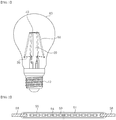
- FIG. 1 is a schematic front view illustrating an LED lamp according to one embodiment of the present disclosure.
- the LED lamp includes a bulb base 10, a center pillar 20, a lower lead wire 30, an upper lead wire 40, an LED filament 50 and a light transmissive bulb 60.
- the bulb base 10 has the same electrode structure as that used in a conventional light bulb.
- passive and active devices such as an AC/DC converter may be built in the bulb base 10.
- the LED lamp according to the embodiments of the present disclosure may use a conventional socket, and, accordingly, the installation cost of additional facilities caused by using the LED lamp may be saved.
- the center pillar 20 is fixed to the bulb base 10 and disposed at a center of the LED lamp.
- the center pillar 20 may include a supporter, a pillar, and an upper end.
- the center pillar 20 is for supporting the LED filaments 50, and, for example, may be formed of glass.
- the lower lead wire 30 electrically connects the bulb base 10 and the LED filament 50.
- the lower lead wire 30 is coupled to a lower end portion of the LED filament 50.
- the lower lead wire 30 is connected to each LED filament 50, wherein these lower lead wires 30 are divided into two groups and are connected to two electrodes of the bulb base 10, respectively.
- the upper lead wire 40 is coupled to an upper end portion of the LED filaments 50.
- a single upper lead wire 40 may connect a pair of LED filaments 50 to each other.
- two pairs of LED filaments 50 are shown, with two upper lead wires 40 connecting the two pairs of LED filaments 50 in series.
- the present disclosure is not limited thereto, and a pair or three or more pairs of LED filaments 50 connected to each other through the upper lead wire 40 may be disposed.
- the light transmissive bulb 60 surrounds the LED filament 50 and is separated from an external environment.
- the light transmissive bulb 60 may be formed of glass or plastic.
- the light transmissive bulb 60 may have various shapes, and may have the same shape as the conventional bulb.
- the LED filament 50 is electrically connected to the bulb base 10 through the lower lead wire 30 and the upper lead wire 40.
- a structure of the LED filament 50 will be described in detail with reference to FIG. 2 and FIG. 3 .
- FIG. 2 is a schematic plan view illustrating an LED filament according to one embodiment of the present disclosure
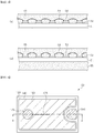
- FIG. 3 shows partially enlarged cross-sectional views of an LED filament according to one embodiment of the present disclosure.
- the LED filament 50 may include a supporting substrate 51, a light emitting diode chip 53, a bonding wire 54, an encapsulant 55, and first and second metal plates 56.
- an adhesive 52 in FIG. 3 ) for bonding the light emitting diode chip 53 to the supporting substrate 51 may be disposed between the light emitting diode chip 53 and the supporting substrate 51.
- the first and second metal plates 56 may also be attached to the supporting substrate 51 using the adhesive.
- the supporting substrate 51 has an elongated shape such as a bar.
- the supporting substrate 51 may also have a first surface and a second surface opposite to the first surface.
- the supporting substrate 51 may be formed of a transparent substance such as sapphire, quartz, or glass, but is not limited thereto, and may be formed of various kinds of transparent or opaque ceramics.
- the LED chips 53 are disposed on the supporting substrate 51.
- the light emitting diode chips 53 may be disposed on, for example, the first surface of the supporting substrate 51, and may be disposed on both surfaces of the first surface and the second surface.
- the light emitting diode chips 53 may be bonded onto the supporting substrate 51 without an adhesive using a wafer bonding technique, or may be bonded onto the supporting substrate 51 using the adhesive 52.
- a transparent adhesive is used for the adhesive 52, and, in a particular embodiment, the adhesive 52 may include wavelength converting substances such as phosphors or quantum dots.
- the bonding wires 54 electrically connect the LED chips 53.
- the LED chips 53 may be connected in series through the bonding wires 54 as shown.
- the upper lead wire 40 of FIG. 1 may connect a pair of LED filaments 50 connected in series in this way to each other in series.
- the LED chips 53 disposed at both end portions are electrically connected to the first and second metal plates 56, respectively.
- These light emitting diode chips 53 may also be electrically connected to the first and second metal plates 56 through the bonding wire 54.
- the encapsulant 55 covers the light emitting diode chips 53, and also covers the bonding wires 54.
- the encapsulant 55 may also partially cover the first and second metal plates 56.
- the encapsulant 55 may cover the LED chips 53 on the first surface of the supporting substrate 51 ( FIG. 3A ), it is not limited thereto, but it may be formed to surround all of the first and second surfaces of the supporting substrates ( FIG. 3B ).
- the encapsulant 55 may contain phosphors converting wavelengths of light emitted from the light emitting diode chips 53. The phosphors contained in the encapsulant will be described in detail later.
- the first and second metal plates 56 are coupled to the supporting substrate 51.
- the first and second metal plates 56 may be attached to the supporting substrate 51 through an adhesive, but are not limited thereto, and may be coupled to the supporting substrate 51 in various ways.
- one end portion of the LED filament 50 is connected to the lower lead wire 30, and the remaining end portion is connected to the upper lead wire 40.
- the first and second metal plates 56 may be coupled to the lower lead wire 30 and the upper lead wire 40 by soldering, welding, or the like.
- the lower lead wire 30 and the upper lead wire 40 may have elasticity, and, accordingly, when the LED filament 40 expands or contracts with heat, the lower and upper lead wires 30 and 40 may bend.
- FIG. 4 is a schematic plan view of a light emitting diode chip 53 mounted on an LED filament according to one embodiment of the present disclosure
- FIG. 5 is a cross-sectional view taken along the line A-A of FIG. 4 .
- the light emitting diode chip 53 may include a growth substrate 110, an n-side semiconductor layer 120, an active layer 130, a p-side semiconductor layer 140, and a transparent electrode 150, an n-electrode 160 and a p-electrode 170.
- the growth substrate 110 is a substrate suitable for growing a gallium nitride-based semiconductor layer, and may be a transparent substrate transmitting light generated in the active layer 130.
- the growth substrate 110 may be a sapphire substrate, a gallium nitride substrate, an aluminum nitride substrate, or the like, and, in particular, may be a patterned sapphire substrate.
- FIG. 5 shows the patterned sapphire substrate, and this substrate 110 has protrusions 115 on a upper surface thereof.
- a semiconductor stacked structure including the n-side semiconductor layer 120, the active layer 130, and the p-side semiconductor layer 140 is disposed on the growth substrate 110.
- the transparent electrode 150 may be disposed on the p-side semiconductor layer 140 to contact the p-side semiconductor layer 140.
- the transparent electrode 150 transmits light generated in the active layer 130.
- the transparent electrode 150 may be formed of a transparent oxide film such as indium-tin-oxide (ITO), ZnO, or the like, or a transparent metal such as Ni/Au, or the like.
- n-electrode 160 is formed on the exposed n-side semiconductor layer 120 and electrically connected to the n-side semiconductor layer 120.
- the n-electrode 160 may be formed of a substance being in ohmic contact with the n-side semiconductor layer 120, and may be formed of, for example, Ti/Al.
- the p-electrode 170 is formed on the transparent electrode 150.
- a portion of the transparent electrode 150 may have an opening exposing the p-side semiconductor layer 140, and the p-electrode 170 may contact the p-side semiconductor layer 140 through the opening formed in the transparent electrode 150.
- the p-electrode 170 may include a reflective layer for reflecting light incident from the active layer 130.
- the p-electrode 170 may be formed of Al/Ti/Pt/Au.
- an extension 175 may extend from the p-electrode 170 toward the n-electrode 160.
- the extension 175 may be formed of the same substance as that of the p-electrode 170 at the same time.
- the semiconductor stacked structure disposed on the growth substrate 110 includes the n-side semiconductor layer 120, the active layer 130 and the p-side semiconductor layer 140 as described above.
- the semiconductor stacked structure described herein may be formed of a gallium nitride-based semiconductor layer, and may be grown on the growth substrate 110 using a metal organic chemical vapor deposition method, a hydride vapor deposition method, or the like.
- the n-side semiconductor layer 120 may have a single layer or a multilayer structure.
- the n-side semiconductor layer 120 may include a buffer layer and an n-type contact layer.
- the buffer layer may be formed of GaN, and may be formed to reduce crystal defects due to lattice mismatch between the growth substrate and the semiconductor layer.
- the active layer 130 may have a single quantum well structure or a multiple quantum well structure.
- the active layer 130 may have a multiple quantum well structure in which a barrier layer and a well layer are alternately stacked, and thus the internal quantum efficiency may be improved.
- the p-side semiconductor layer 140 may have a single layer or a multilayer structure, and may include, for example, an electron blocking layer and a p-type contact layer.
- the electron blocking layer is disposed on the active layer 130, and confines electrons in the active layer 130 to improve recombination rate.
- the electron blocking layer may be formed of AlGaN or AlInGaN.
- the p-type contact layer is a layer doped with a p-type impurity such as Mg, and the transparent electrode 150 is electrically connected to the p-type contact layer.
- the present disclosure is not limited to the light emitting diode chip described herein, but various kinds of blue light emitting diode chips may be used.
- the light emitting diode chip 53 may have a light emission peak in the blue region, for example, in a range of 450 nm to 470 nm, and further in a range of 450 nm to 460 nm.
- phosphors contained in the encapsulant 55 emit light converted and excited by light emitted from the light emitting diode chip 53.
- the phosphor includes a green phosphor having an emission peak in a range of 500 nm to 550 nm and a red phosphor having an emission peak in a range of 600 nm to 650 nm.
- the red phosphor includes a first red phosphor having an emission peak in a range of 620 nm to 630 nm and a second red phosphor having an emission peak in a range of 630 nm to 640 nm.
- Full widths at half maximum of the first red phosphor and the second red phosphor may be in a range of 20 nm to 60 nm, respectively, and may be further, in a range of 40 nm to 60 nm, specifically, in a range of 50 nm to 60 nm.
- the first and second red phosphors may be, for example, (Ca, Sr)S:Eu2+ -based sulfide phosphors, but are not necessarily limited thereto.
- the red phosphor having the full width at half maximum of 20 nm to 60 nm may improve R8 without reducing the luminous intensity of the lighting apparatus because a tail region of the unnecessary wavelength band is small. Moreover, since the full width at half maximum is not extremely narrow like that of the KSF phosphor, there is no need to increase an amount of the phosphor used to improve R8.
- the first red phosphor having the emission peak in the range of 620 nm to 630 nm and the second red phosphor having the emission peak in the range of 630 nm to 640 nm are used together, and thus a relatively large region of the red region to improve R8 may be easily covered. Accordingly, it is possible to reduce the amount of phosphor used for achieving an equivalent Ra compared to using a nitride-based phosphor.
- the green phosphor has an emission peak in a range of 500 nm to 550 nm.
- the green phosphor is not particularly limited, but a Lu 3 (Al,Ga) 5 O 12 :Ce (LuAG)-based phosphor, a silicate phosphor such as Ba 2 MgSi 2 O 7 :Eu 2+ , Ba 2 SiO 4 :Eu 2+ , Ca 3 (Sc,Mg) 2 Si 3 O 12 :Ce 3+ , or the like or a sulfide phosphor such as (Sr,Ca)Ga 2 S 4 :Eu 2+ , or the like may be used, for example.
- the green phosphor may have a full width at half maximum in a range of 90 nm to 130 nm, thereby covering a relatively wide wavelength region.
- the phosphor may further include a yellow phosphor.
- a YAG phosphor or a silicate phosphor may be used.
- the yellow phosphor may have an emission peak in a range of 550 nm to 600 nm, and may have a wide full width at half maximum of 100 nm or more like the green phosphor.
- FIG. 6 is a graph showing luminous fluxes and R8s of lighting apparatuses according to comparative examples and an exemplary embodiment.
- LED chips of the same type were disposed on a supporting substrate, and the supporting substrate was wrapped with an encapsulant containing a phosphor.
- a red phosphor homologous LuAG-based phosphors and YAG phosphors were used.
- two kinds of nitride-based phosphors were used as red phosphors, and two kinds (Ca, Sr)S:Eu 2+ sulfide phosphors as red phosphors were used for the exemplary embodiment.
- the nitride-based phosphors had emission peaks of about 635 nm and 646 nm, and full widths at half maximum thereof were about 92.5 nm and 87.5 nm, respectively.
- the sulfide phosphors had emission peaks of about 626 nm and 634 nm, and full widths at half maximum thereof were about 53.5 nm and about 56.5 nm, respectively.
- Comparative Example 1 having a Ra (CRI) of about 80 and Comparative Example 2 having a Ra (CRI) of about 90 and Exemplary Embodiment 1 having a Ra of about 80.
- the lighting apparatus of Comparative Example 1 having Ra of 80 had R8 of less than 60
- lighting apparatus of Comparative Example 2 having Ra of 90 had R8 of 80 or more
- Ra was 80 and R8 was 72 or more.
- FIG. 7 is a graph showing amounts of phosphors used in lighting apparatuses.
- Comparative Example 1 and Exemplary Embodiment 1 are the same as described above, and Comparative Example 3 uses a KSF phosphor as a red phosphor.
- the KSF phosphor was used more than six times, almost seven times, and an amount of the sulfide phosphor used was lower than that of the nitride phosphor.
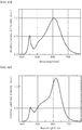
- FIG. 8A and FIG. 8B are graphs showing emission spectra of Comparative Example 1 and Exemplary Embodiment 1.
- the luminous intensity of the red light wavelength region is improved. Furthermore, since the phosphors having the narrow full widths at half maximum are used, tails generated on a side of the long wavelength may be reduced, and thus the luminous intensity may be increased while improving R8.
Landscapes
- Chemical & Material Sciences (AREA)
- Engineering & Computer Science (AREA)
- Inorganic Chemistry (AREA)
- Materials Engineering (AREA)
- Organic Chemistry (AREA)
- Physics & Mathematics (AREA)
- Microelectronics & Electronic Packaging (AREA)
- Optics & Photonics (AREA)
- General Engineering & Computer Science (AREA)
- Led Device Packages (AREA)
- Led Devices (AREA)
- Non-Portable Lighting Devices Or Systems Thereof (AREA)
Abstract
Description
- Embodiments of the present disclosure relate to a lighting apparatus, and, more particularly, to an LED lighting apparatus and an LED filament having improved color rendering.
- Light bulbs in the related art generate light using metal filaments such as tungsten. However, light bulbs with metal filaments have been quickly being replaced by LED lamps because of their short lifespan, low light efficiency, and high power consumption.
- An LED lighting apparatus such as an LED lamp generally uses LEDs that emit light in the blue region as a light source. In particular, the LED lighting apparatus that implements white light uses a phosphor along with the LEDs.
- Meanwhile, high color rendering is generally required for lighting apparatuses that implement white light. Color rendering is a property of an illumination light source that indicates how similar an object color irradiated by the lighting apparatus is to an object color irradiated by a reference light source. The color rendering is evaluated by the color rendering index (CRI), and a general color rendering index (Ra) is widely used. Ra is the average value of the individual color rendering indices (special CRIs; R1 to R8) quantified using eight test color samples.
- In general, when Ra exhibits a high value, it is recognized that the color rendering of the illumination light source is high. However, increasing Ra in the lighting apparatus using a blue LED as the light source generally leads to a decrease in the luminous intensity, thereby increasing the power consumption. Furthermore, since Ra is the average value of individual color rendering indices, high Ra does not necessarily mean that R1 to R8 are all evenly high. In particular, since the LED lighting apparatus using the blue LED lacks light in the red region, the value of R8 measured using a test color sample having a high reflectance in the pink region is generally relatively low compared to R1 to R7. Therefore, there is a need for an LED lighting apparatus capable of increasing R8 while achieving appropriate Ra.
- Although the phosphor in the red region is added to sufficiently increase the value of R8, unnecessary light is generated due to a considerable amount of tail generated in the emission spectrum of the red phosphor, thereby deteriorating the efficiency of the lighting apparatus. A mainly used nitride-based red phosphor, such as CaAlSiN3:Eu2+, has a full width at half maximum of about 80 nm or more, and when a nitride phosphor having an emission peak of about 650 nm is used, a considerable amount of light is generated even in a region of 700 nm or more. Accordingly, when the amount of red phosphor is increased to increase R8, Ra is increased as a whole and the overall luminous intensity of the lighting apparatus is lowered. That is, it is difficult to increase R8 without reducing the luminous intensity of the lighting apparatus with the nitride-based red phosphor. In addition, although the luminous intensity may be increased by increasing the number of lighting apparatuses or increasing the number of LEDs and an amount of phosphors in the lighting apparatus, since the power consumption increases, this is not a desirable measure.
- Recently, K2SiF6:Mn4+(KSF) has been used as the red phosphor having a narrow full width at half maximum. The KSF phosphor has a very narrow full width at half maximum of less than about 10 nm, and, accordingly, is a phosphor capable of implementing good color reproducibility. When using the red phosphor having the narrow full width at half maximum such as KSF, it is possible to remove unnecessary tails and emit light in the desired red region, thereby achieving high R8 even with relatively low Ra. That is, appropriate Ra and R8 may be achieved without significantly reducing the luminous intensity. However, since the full width at half maximum is narrow, there is a problem that an amount of the KSF phosphor used is more considerably increased than when the nitride-based red phosphor is used. In general, when the KSF phosphor is used, since the amount of phosphor used is increased by six times or more than when using the nitride-based phosphor, increasing R8 by using KSF is not a proper choice. In addition, the KSF phosphor is relatively expensive compared to other red phosphors and difficult to purchase as a phosphor, and thus there are many restrictions to use it.
- Embodiments of the present disclosure provide a new LED lighting apparatus to improve R8 while preventing the reduction of the luminous intensity of the lighting apparatus.
- Embodiments of the present disclosure provide an LED lighting apparatus capable of increasing R8 without increasing an amount of phosphor used.
- A lighting apparatus according to one embodiment of the present disclosure includes: a light emitting diode chip emitting blue light; a green phosphor having an emission peak in a range of 500 nm to 550 nm; and a red phosphor having an emission peak in a range of 600 nm to 650nm, wherein the red phosphor includes: a first red phosphor having an emission peak in a range of 620 nm to 630 nm; and a second red phosphor having an emission peak in a range of 630 nm to 640 nm, wherein full widths at half maximum of the first red phosphor and the second red phosphor are in a range of 20 nm to 60 nm, respectively.
- In particular, Ra may be in a range of 80 to 98, and R8 may be greater than 72.
- The first red phosphor and the second red phosphor may be (Ca, Sr)S:Eu-based phosphors. However, the present disclosure is not limited to a specific sulfide phosphor, and other red phosphors whose emission peak and full width at half maximum satisfy the above condition may be used.
- In a particular embodiment, full widths at half maximum of the first red phosphor and the second red phosphor may be in a range of 50 nm to 60 nm.
- Meanwhile, the green phosphor may include a Lu3(Al, Ga)5O12:Ce (LuAG)-based phosphor.
- Moreover, the lighting apparatus may further include a yellow phosphor having an emission peak in a range of 550 nm to 600 nm.
- A mixing ratio of the green phosphor, the yellow phosphor and the red phosphor may be adjusted, and thus it is possible to satisfy a required color rendering index. In addition, since two kinds of red phosphors having a relatively narrow full width at half maximum are used, R8 may be achieved without reducing the luminous intensity.
- The lighting apparatus may include an LED filament. The LED filament may include: a supporting substrate; a plurality of light emitting diode chips adhered to the supporting substrate; wires electrically connecting the LED chips; and an encapsulant for encapsulating the plurality of LED chips, wherein the green phosphor and red phosphor may be distributed in the encapsulant. Further, the encapsulant may surround the supporting substrate.
- An LED filament according to another embodiment may include: a supporting substrate; a plurality of light emitting diode chips disposed on the supporting substrate, and emitting blue light; and an encapsulant covering the plurality of light emitting diode chips and having phosphors distributed therein, wherein the phosphors may include: a green phosphor having an emission peak in a range of 500 nm to 550 nm; and a red phosphor having an emission peak in a range of 600 nm to 650nm, wherein the red phosphor may include: a first red phosphor having an emission peak in a range of 620 nm to 630 nm; and a second red phosphor having an emission peak in a range of 630 nm to 640 nm, wherein full widths at half maximum of the first red phosphor and the second red phosphor are in a range of 20 nm to 60 nm, respectively.
- Ra of the LED filament may be in a range of 80 to 98, and R8 may be greater than 72.
- In addition, the first red phosphor and the second red phosphor may be (Ca, Sr)S:Eu- based phosphors.
- Furthermore, full widths at half maximum of the first red phosphor and the second red phosphor may be in a range of 50 nm to 60 nm.
- According to embodiments of the present disclosure, since two kinds of red phosphors having full widths at half maximum in a range of 20 nm to 60 nm are used, favorable color rendering with R8 of 72 or more may be achieved without increasing an amount of phosphors used, thereby preventing the luminous intensity of a lighting apparatus from being reduced.
-
-
FIG. 1 is a schematic front view illustrating an LED lamp according to one embodiment of the present disclosure. -
FIG. 2 is a schematic plan view illustrating an LED filament according to one embodiment of the present disclosure. -
FIG. 3 show partially enlarged cross-sectional views of an LED filament according to one embodiment of the present disclosure. -
FIG. 4 is a schematic plan view of a light emitting diode chip mounted on an LED filament according to one embodiment of the present disclosure. -
FIG. 5 is a cross-sectional view taken along the line A-A ofFIG. 4 . -
FIG. 6 is a graph showing luminous fluxes and R8s of lighting apparatuses according to comparative examples and an exemplary embodiment. -
FIG. 7 is a graph showing amounts of phosphors used in lighting apparatuses. -
FIG. 8A and FIG. 8B are graphs showing emission spectra of a comparative example and an exemplary embodiment. - Hereinafter, embodiments of the present disclosure will be described in detail with reference to the accompanying drawings. The following embodiments are provided by way of example so as to fully convey the spirit of the present disclosure to those skilled in the art to which the present disclosure pertains. Accordingly, the present disclosure is not limited to the embodiments disclosed herein and can also be implemented in different forms. In the drawings, widths, lengths, thicknesses, and the like of elements can be exaggerated for clarity and descriptive purposes. When an element or layer is referred to as being "disposed above" or "disposed on" another element or layer, it can be directly "disposed above" or "disposed on" the other element or layer or intervening elements or layers can be present. Throughout the specification, like reference numerals denote like elements having the same or similar functions.
- Although an LED lamp is exemplarily described below as an example of an LED lighting apparatus, it should be understood that the lighting apparatus of the present disclosure is not limited to the LED lamp described below, but may be embodied in various types of lighting apparatuses.
-
FIG. 1 is a schematic front view illustrating an LED lamp according to one embodiment of the present disclosure. - Referring to
FIG. 1 , the LED lamp includes abulb base 10, acenter pillar 20, alower lead wire 30, anupper lead wire 40, anLED filament 50 and alight transmissive bulb 60. - The
bulb base 10 has the same electrode structure as that used in a conventional light bulb. In addition, passive and active devices such as an AC/DC converter may be built in thebulb base 10. - Since the
bulb base 10 has the same electrode structure as the conventional bulb, the LED lamp according to the embodiments of the present disclosure may use a conventional socket, and, accordingly, the installation cost of additional facilities caused by using the LED lamp may be saved. - The
center pillar 20 is fixed to thebulb base 10 and disposed at a center of the LED lamp. Thecenter pillar 20 may include a supporter, a pillar, and an upper end. Thecenter pillar 20 is for supporting theLED filaments 50, and, for example, may be formed of glass. - The
lower lead wire 30 electrically connects thebulb base 10 and theLED filament 50. Thelower lead wire 30 is coupled to a lower end portion of theLED filament 50. Thelower lead wire 30 is connected to eachLED filament 50, wherein theselower lead wires 30 are divided into two groups and are connected to two electrodes of thebulb base 10, respectively. - Meanwhile, the
upper lead wire 40 is coupled to an upper end portion of theLED filaments 50. A singleupper lead wire 40 may connect a pair ofLED filaments 50 to each other. In this embodiment, two pairs ofLED filaments 50 are shown, with twoupper lead wires 40 connecting the two pairs ofLED filaments 50 in series. However, the present disclosure is not limited thereto, and a pair or three or more pairs ofLED filaments 50 connected to each other through theupper lead wire 40 may be disposed. - The
light transmissive bulb 60 surrounds theLED filament 50 and is separated from an external environment. Thelight transmissive bulb 60 may be formed of glass or plastic. Thelight transmissive bulb 60 may have various shapes, and may have the same shape as the conventional bulb. - Meanwhile, the
LED filament 50 is electrically connected to thebulb base 10 through thelower lead wire 30 and theupper lead wire 40. A structure of theLED filament 50 will be described in detail with reference toFIG. 2 andFIG. 3 . -
FIG. 2 is a schematic plan view illustrating an LED filament according to one embodiment of the present disclosure, andFIG. 3 shows partially enlarged cross-sectional views of an LED filament according to one embodiment of the present disclosure. - Referring to
FIG. 2 andFIG. 3 , theLED filament 50 may include a supportingsubstrate 51, a light emittingdiode chip 53, abonding wire 54, anencapsulant 55, and first andsecond metal plates 56. In addition, an adhesive (52 inFIG. 3 ) for bonding the light emittingdiode chip 53 to the supportingsubstrate 51 may be disposed between the light emittingdiode chip 53 and the supportingsubstrate 51. In addition, although not shown, the first andsecond metal plates 56 may also be attached to the supportingsubstrate 51 using the adhesive. - The supporting
substrate 51 has an elongated shape such as a bar. The supportingsubstrate 51 may also have a first surface and a second surface opposite to the first surface. The supportingsubstrate 51 may be formed of a transparent substance such as sapphire, quartz, or glass, but is not limited thereto, and may be formed of various kinds of transparent or opaque ceramics. - The LED chips 53 are disposed on the supporting
substrate 51. The light emittingdiode chips 53 may be disposed on, for example, the first surface of the supportingsubstrate 51, and may be disposed on both surfaces of the first surface and the second surface. The light emittingdiode chips 53 may be bonded onto the supportingsubstrate 51 without an adhesive using a wafer bonding technique, or may be bonded onto the supportingsubstrate 51 using the adhesive 52. In one embodiment, a transparent adhesive is used for the adhesive 52, and, in a particular embodiment, the adhesive 52 may include wavelength converting substances such as phosphors or quantum dots. - Meanwhile, the
bonding wires 54 electrically connect the LED chips 53. The LED chips 53 may be connected in series through thebonding wires 54 as shown. Theupper lead wire 40 ofFIG. 1 may connect a pair ofLED filaments 50 connected in series in this way to each other in series. Meanwhile, the LED chips 53 disposed at both end portions are electrically connected to the first andsecond metal plates 56, respectively. These light emittingdiode chips 53 may also be electrically connected to the first andsecond metal plates 56 through thebonding wire 54. - The
encapsulant 55 covers the light emittingdiode chips 53, and also covers thebonding wires 54. Theencapsulant 55 may also partially cover the first andsecond metal plates 56. Although theencapsulant 55 may cover the LED chips 53 on the first surface of the supporting substrate 51 (FIG. 3A ), it is not limited thereto, but it may be formed to surround all of the first and second surfaces of the supporting substrates (FIG. 3B ). Theencapsulant 55 may contain phosphors converting wavelengths of light emitted from the light emitting diode chips 53. The phosphors contained in the encapsulant will be described in detail later. - The first and
second metal plates 56 are coupled to the supportingsubstrate 51. The first andsecond metal plates 56 may be attached to the supportingsubstrate 51 through an adhesive, but are not limited thereto, and may be coupled to the supportingsubstrate 51 in various ways. - Meanwhile, as described with reference to
FIG. 1 , one end portion of theLED filament 50 is connected to thelower lead wire 30, and the remaining end portion is connected to theupper lead wire 40. In this case, the first andsecond metal plates 56 may be coupled to thelower lead wire 30 and theupper lead wire 40 by soldering, welding, or the like. - In addition, the
lower lead wire 30 and theupper lead wire 40 may have elasticity, and, accordingly, when theLED filament 40 expands or contracts with heat, the lower andupper lead wires -
FIG. 4 is a schematic plan view of a light emittingdiode chip 53 mounted on an LED filament according to one embodiment of the present disclosure, andFIG. 5 is a cross-sectional view taken along the line A-A ofFIG. 4 . - Referring to
FIG. 4 andFIG. 5 , the light emittingdiode chip 53 may include agrowth substrate 110, an n-side semiconductor layer 120, anactive layer 130, a p-side semiconductor layer 140, and atransparent electrode 150, an n-electrode 160 and a p-electrode 170. - The
growth substrate 110 is a substrate suitable for growing a gallium nitride-based semiconductor layer, and may be a transparent substrate transmitting light generated in theactive layer 130. For example, thegrowth substrate 110 may be a sapphire substrate, a gallium nitride substrate, an aluminum nitride substrate, or the like, and, in particular, may be a patterned sapphire substrate.FIG. 5 shows the patterned sapphire substrate, and thissubstrate 110 hasprotrusions 115 on a upper surface thereof. - A semiconductor stacked structure including the n-
side semiconductor layer 120, theactive layer 130, and the p-side semiconductor layer 140 is disposed on thegrowth substrate 110. - The
transparent electrode 150 may be disposed on the p-side semiconductor layer 140 to contact the p-side semiconductor layer 140. Thetransparent electrode 150 transmits light generated in theactive layer 130. Thetransparent electrode 150 may be formed of a transparent oxide film such as indium-tin-oxide (ITO), ZnO, or the like, or a transparent metal such as Ni/Au, or the like. - Meanwhile, portions of the p-
side semiconductor layer 140 and theactive layer 130 may be removed to expose the n-side semiconductor layer 120. The n-electrode 160 is formed on the exposed n-side semiconductor layer 120 and electrically connected to the n-side semiconductor layer 120. The n-electrode 160 may be formed of a substance being in ohmic contact with the n-side semiconductor layer 120, and may be formed of, for example, Ti/Al. - The p-
electrode 170 is formed on thetransparent electrode 150. A portion of thetransparent electrode 150 may have an opening exposing the p-side semiconductor layer 140, and the p-electrode 170 may contact the p-side semiconductor layer 140 through the opening formed in thetransparent electrode 150. The p-electrode 170 may include a reflective layer for reflecting light incident from theactive layer 130. For example, the p-electrode 170 may be formed of Al/Ti/Pt/Au. - Meanwhile, an
extension 175 may extend from the p-electrode 170 toward the n-electrode 160. Theextension 175 may be formed of the same substance as that of the p-electrode 170 at the same time. - The semiconductor stacked structure disposed on the
growth substrate 110 includes the n-side semiconductor layer 120, theactive layer 130 and the p-side semiconductor layer 140 as described above. The semiconductor stacked structure described herein may be formed of a gallium nitride-based semiconductor layer, and may be grown on thegrowth substrate 110 using a metal organic chemical vapor deposition method, a hydride vapor deposition method, or the like. - Meanwhile, the n-
side semiconductor layer 120 may have a single layer or a multilayer structure. For example, the n-side semiconductor layer 120 may include a buffer layer and an n-type contact layer. The buffer layer may be formed of GaN, and may be formed to reduce crystal defects due to lattice mismatch between the growth substrate and the semiconductor layer. - Meanwhile, the
active layer 130 may have a single quantum well structure or a multiple quantum well structure. In particular, theactive layer 130 may have a multiple quantum well structure in which a barrier layer and a well layer are alternately stacked, and thus the internal quantum efficiency may be improved. - The p-
side semiconductor layer 140 may have a single layer or a multilayer structure, and may include, for example, an electron blocking layer and a p-type contact layer. - The electron blocking layer is disposed on the
active layer 130, and confines electrons in theactive layer 130 to improve recombination rate. The electron blocking layer may be formed of AlGaN or AlInGaN. - The p-type contact layer is a layer doped with a p-type impurity such as Mg, and the
transparent electrode 150 is electrically connected to the p-type contact layer. - Although an example of the light emitting
diode chip 53 has been described, the present disclosure is not limited to the light emitting diode chip described herein, but various kinds of blue light emitting diode chips may be used. - Meanwhile, the light emitting
diode chip 53 may have a light emission peak in the blue region, for example, in a range of 450 nm to 470 nm, and further in a range of 450 nm to 460 nm. Meanwhile, phosphors contained in theencapsulant 55 emit light converted and excited by light emitted from the light emittingdiode chip 53. - In particular, the phosphor includes a green phosphor having an emission peak in a range of 500 nm to 550 nm and a red phosphor having an emission peak in a range of 600 nm to 650 nm. Further, in the present embodiment, the red phosphor includes a first red phosphor having an emission peak in a range of 620 nm to 630 nm and a second red phosphor having an emission peak in a range of 630 nm to 640 nm. Full widths at half maximum of the first red phosphor and the second red phosphor may be in a range of 20 nm to 60 nm, respectively, and may be further, in a range of 40 nm to 60 nm, specifically, in a range of 50 nm to 60 nm. The first and second red phosphors may be, for example, (Ca, Sr)S:Eu2+ -based sulfide phosphors, but are not necessarily limited thereto.
- The red phosphor having the full width at half maximum of 20 nm to 60 nm may improve R8 without reducing the luminous intensity of the lighting apparatus because a tail region of the unnecessary wavelength band is small. Moreover, since the full width at half maximum is not extremely narrow like that of the KSF phosphor, there is no need to increase an amount of the phosphor used to improve R8.
- Furthermore, the first red phosphor having the emission peak in the range of 620 nm to 630 nm and the second red phosphor having the emission peak in the range of 630 nm to 640 nm are used together, and thus a relatively large region of the red region to improve R8 may be easily covered. Accordingly, it is possible to reduce the amount of phosphor used for achieving an equivalent Ra compared to using a nitride-based phosphor.
- Meanwhile, the green phosphor has an emission peak in a range of 500 nm to 550 nm. The green phosphor is not particularly limited, but a Lu3(Al,Ga)5O12:Ce (LuAG)-based phosphor, a silicate phosphor such as Ba2MgSi2O7:Eu2+, Ba2SiO4:Eu2+, Ca3(Sc,Mg)2Si3O12:Ce3+, or the like or a sulfide phosphor such as (Sr,Ca)Ga2S4:Eu2+, or the like may be used, for example. In particular, the green phosphor may have a full width at half maximum in a range of 90 nm to 130 nm, thereby covering a relatively wide wavelength region.
- Meanwhile, the phosphor may further include a yellow phosphor. For example, a YAG phosphor or a silicate phosphor may be used. The yellow phosphor may have an emission peak in a range of 550 nm to 600 nm, and may have a wide full width at half maximum of 100 nm or more like the green phosphor.
-
FIG. 6 is a graph showing luminous fluxes and R8s of lighting apparatuses according to comparative examples and an exemplary embodiment. - In the lighting apparatus of the comparative examples and that of the exemplary embodiment, LED chips of the same type were disposed on a supporting substrate, and the supporting substrate was wrapped with an encapsulant containing a phosphor. In addition, except for a red phosphor, homologous LuAG-based phosphors and YAG phosphors were used. Meanwhile, for the comparative example, two kinds of nitride-based phosphors were used as red phosphors, and two kinds (Ca, Sr)S:Eu2+ sulfide phosphors as red phosphors were used for the exemplary embodiment.
- The nitride-based phosphors had emission peaks of about 635 nm and 646 nm, and full widths at half maximum thereof were about 92.5 nm and 87.5 nm, respectively. In contrast, the sulfide phosphors had emission peaks of about 626 nm and 634 nm, and full widths at half maximum thereof were about 53.5 nm and about 56.5 nm, respectively.
- A mixing ratio of these phosphors was adjusted to prepare Comparative Example 1 having a Ra (CRI) of about 80 and Comparative Example 2 having a Ra (CRI) of about 90 and
Exemplary Embodiment 1 having a Ra of about 80. - When the luminous flux of the lighting apparatus of Comparative Example 1 having Ra of 80 was 100, the luminous flux of Comparative Example 2 having Ra of 90 was reduced by 10% or more compared with Comparative Example 1. In contrast, the luminous flux of the lighting apparatus of
Exemplary Embodiment 1 having Ra of 80 was slightly reduced compared with Comparative Example 1. - Meanwhile, the lighting apparatus of Comparative Example 1 having Ra of 80 had R8 of less than 60, and lighting apparatus of Comparative Example 2 having Ra of 90 had R8 of 80 or more. Meanwhile, for the
Exemplary Embodiment 1, Ra was 80 and R8 was 72 or more. - That is, according to
Exemplary Embodiment 1, two kinds of red phosphors having relatively small full widths at half maximum were mixed to use, and thus it was possible to increase R8 of 72 or more while keeping Ra relatively low. On the other hand, when using nitride-based phosphors having relatively large full widths at half maximum as in Comparative Examples 1 and 2, it can be seen that Ra needs to be increased so as to achieve high R8, and thus the luminous flux is considerably reduced. -
FIG. 7 is a graph showing amounts of phosphors used in lighting apparatuses. - To achieve the
same Ra 80, the amount of phosphors used in the lighting apparatus was compared. Comparative Example 1 andExemplary Embodiment 1 are the same as described above, and Comparative Example 3 uses a KSF phosphor as a red phosphor. - When the amount of the nitride phosphor was 100%, the KSF phosphor was used more than six times, almost seven times, and an amount of the sulfide phosphor used was lower than that of the nitride phosphor.
-
FIG. 8A and FIG. 8B are graphs showing emission spectra of Comparative Example 1 andExemplary Embodiment 1. - As can be seen from
FIG. 8A and FIG. 8B , when the red phosphor ofExemplary embodiment 1 having the narrow full width at half maximum is used, the luminous intensity of the red light wavelength region is improved. Furthermore, since the phosphors having the narrow full widths at half maximum are used, tails generated on a side of the long wavelength may be reduced, and thus the luminous intensity may be increased while improving R8. - Although some embodiments have been described herein, it should be understood that these embodiments are provided for illustration only and are not to be construed in any way as limiting the present disclosure. It should be understood that features or components of one embodiment can also be applied to other embodiments without departing from the spirit and scope of the present disclosure.
Claims (13)
- A lighting apparatus, comprising:a light emitting diode chip emitting blue light;a green phosphor having an emission peak in a range of 500 nm to 550 nm; anda red phosphor having an emission peak in a range of 600 nm to 650nm,wherein the red phosphor comprises:a first red phosphor having an emission peak in a range of 620 nm to 630 nm; and a second red phosphor having an emission peak in a range of 630 nm to 640 nm, wherein full widths at half maximum of the first red phosphor and the second red phosphor are in a range of 20 nm to 60 nm, respectively.
- The lighting apparatus of claim 1,
wherein Ra is in a range of 80 to 98, and R8 is greater than 72. - The lighting apparatus of claim 1,
wherein the first red phosphor and the second red phosphor are (Ca, Sr)S:Eu-based phosphors. - The lighting apparatus of claim 3,
wherein full widths at half maximum of the first red phosphor and the second red phosphor are in a range of 50 nm to 60 nm. - The lighting apparatus of claim 5,
wherein the green phosphor includes a Lu3 (Al, Ga)5O12: Ce (LuAG)-based phosphor. - The lighting apparatus of claim 1, further comprising:
a yellow phosphor having an emission peak in a range of 550 nm to 600 nm. - The lighting apparatus of claim 1,
wherein the lighting apparatus is an LED lamp including an LED filament. - The lighting apparatus of claim 7,
wherein the LED filament comprises:
a supporting substrate;
a plurality of light emitting diode chips adhered to the supporting substrate;
wires electrically connecting the LED chips; and
an encapsulant for encapsulating the plurality of LED chips,
wherein the green phosphor and red phosphor are distributed in the encapsulant. - The lighting apparatus of claim 8,
wherein the encapsulant surrounds the supporting substrate. - An LED filament, comprising:a supporting substrate;a plurality of light emitting diode chips disposed on the supporting substrate, and emitting blue light; andan encapsulant covering the plurality of light emitting diode chips and having phosphors distributed therein,wherein the phosphors comprise:a green phosphor having an emission peak in a range of 500 nm to 550 nm; and a red phosphor having an emission peak in a range of 600 nm to 650nm, wherein the red phosphor comprises:a first red phosphor having an emission peak in a range of 620 nm to 630 nm; anda second red phosphor having an emission peak in a range of 630 nm to 640 nm,wherein full widths at half maximum of the first red phosphor and the second red phosphor are in a range of 20 nm to 60 nm, respectively.
- The LED filament of claim 10,
wherein Ra is in a range of 80 to 98, and R8 is greater than 72. - The LED filament of claim 10,
wherein the first red phosphor and the second red phosphor are (Ca, Sr)S:Eu-based phosphors. - The LED filament of claim 12,
wherein full widths at half maximum of the first red phosphor and the second red phosphor are in a range of 50 nm to 60 nm.
Applications Claiming Priority (2)
| Application Number | Priority Date | Filing Date | Title |
|---|---|---|---|
| KR1020180022178A KR20190101787A (en) | 2018-02-23 | 2018-02-23 | Led lighting apparatus having improved color lendering and led filament |
| PCT/KR2019/001534 WO2019164160A1 (en) | 2018-02-23 | 2019-02-07 | Led lighting apparatus having improved color rendering, and led filament |
Publications (4)
| Publication Number | Publication Date |
|---|---|
| EP3657064A1 true EP3657064A1 (en) | 2020-05-27 |
| EP3657064A4 EP3657064A4 (en) | 2021-04-21 |
| EP3657064B1 EP3657064B1 (en) | 2024-06-12 |
| EP3657064C0 EP3657064C0 (en) | 2024-06-12 |
Family
ID=67687789
Family Applications (1)
| Application Number | Title | Priority Date | Filing Date |
|---|---|---|---|
| EP19756490.9A Active EP3657064B1 (en) | 2018-02-23 | 2019-02-07 | Led lighting apparatus having improved color rendering, and led filament |
Country Status (6)
| Country | Link |
|---|---|
| US (3) | US11527682B2 (en) |
| EP (1) | EP3657064B1 (en) |
| KR (2) | KR20190101787A (en) |
| CN (2) | CN112436085A (en) |
| DE (1) | DE212019000109U1 (en) |
| WO (1) | WO2019164160A1 (en) |
Families Citing this family (2)
| Publication number | Priority date | Publication date | Assignee | Title |
|---|---|---|---|---|
| CN113615320B (en) | 2019-03-29 | 2024-08-30 | 索尼集团公司 | Light-emitting device, display and electronic device |
| US11295680B2 (en) * | 2019-04-11 | 2022-04-05 | PixelDisplay, Inc. | Method and apparatus of a multi-modal illumination and display for improved color rendering, power efficiency, health and eye-safety |
Family Cites Families (20)
| Publication number | Priority date | Publication date | Assignee | Title |
|---|---|---|---|---|
| TW200523340A (en) * | 2003-09-24 | 2005-07-16 | Patent Treuhand Ges Fur Elek Sche Gluhlampen Mbh | Hochefeizienter leuchtstoff |
| KR100887489B1 (en) | 2004-04-27 | 2009-03-10 | 파나소닉 주식회사 | Phosphor composition and method for producing the same, and light-emitting device using the same |
| US8417215B2 (en) | 2004-07-28 | 2013-04-09 | Koninklijke Philips Electronics N.V. | Method for positioning of wireless medical devices with short-range radio frequency technology |
| US7453195B2 (en) * | 2004-08-02 | 2008-11-18 | Lumination Llc | White lamps with enhanced color contrast |
| KR101319209B1 (en) * | 2006-11-24 | 2013-10-16 | 엘지디스플레이 주식회사 | Backlight unit of liquid crystal display device |
| KR100900620B1 (en) | 2007-02-20 | 2009-06-02 | 삼성전기주식회사 | White light emitting device |
| US20100289044A1 (en) * | 2009-05-12 | 2010-11-18 | Koninklijke Philips Electronics N.V. | Wavelength conversion for producing white light from high power blue led |
| US8508127B2 (en) | 2010-03-09 | 2013-08-13 | Cree, Inc. | High CRI lighting device with added long-wavelength blue color |
| JP5189211B2 (en) * | 2010-07-20 | 2013-04-24 | パナソニック株式会社 | Light bulb shaped lamp |
| US8921875B2 (en) | 2011-05-10 | 2014-12-30 | Cree, Inc. | Recipient luminophoric mediums having narrow spectrum luminescent materials and related semiconductor light emitting devices and methods |
| US20140218892A1 (en) * | 2013-02-05 | 2014-08-07 | Intematix Corporation | Wide emission angle led package with remote phosphor component |
| US9915775B2 (en) | 2013-08-29 | 2018-03-13 | Soraa, Inc. | Circadian-friendly LED light sources |
| TWI610465B (en) * | 2013-10-07 | 2018-01-01 | Epistar Corporation | Light-emitting diode assembly and manufacturing method |
| US9871173B2 (en) * | 2015-06-18 | 2018-01-16 | Cree, Inc. | Light emitting devices having closely-spaced broad-spectrum and narrow-spectrum luminescent materials and related methods |
| US10363325B2 (en) * | 2015-06-26 | 2019-07-30 | Kenall Manufacturing Company | Lighting device that deactivates dangerous pathogens while providing visually appealing light |
| GB2543139B (en) | 2015-08-17 | 2018-05-23 | Jiaxing Super Lighting Electric Appliance Co Ltd | LED light bulb and LED filament thereof |
| EP3368634B1 (en) * | 2015-10-29 | 2019-12-11 | Signify Holding B.V. | Improved white lighting device for retail illumination |
| EP3523394A2 (en) * | 2017-07-26 | 2019-08-14 | Merck Patent GmbH | Phosphor and a composition |
| CN107946434B (en) * | 2017-11-27 | 2021-03-26 | 广东晶科电子股份有限公司 | White Light Emitting Diodes and Backlight Modules |
| JP7377823B2 (en) * | 2018-02-27 | 2023-11-10 | シグニファイ ホールディング ビー ヴィ | LED filament lamp with control unit |
-
2018
- 2018-02-23 KR KR1020180022178A patent/KR20190101787A/en not_active Ceased
-
2019
- 2019-02-07 US US16/649,144 patent/US11527682B2/en active Active
- 2019-02-07 CN CN202011328264.1A patent/CN112436085A/en not_active Withdrawn
- 2019-02-07 WO PCT/KR2019/001534 patent/WO2019164160A1/en not_active Ceased
- 2019-02-07 CN CN201980000929.5A patent/CN110402498B/en active Active
- 2019-02-07 DE DE212019000109.2U patent/DE212019000109U1/en active Active
- 2019-02-07 EP EP19756490.9A patent/EP3657064B1/en active Active
-
2022
- 2022-12-05 US US18/075,330 patent/US12218290B2/en active Active
-
2023
- 2023-07-26 KR KR1020230097433A patent/KR20230118056A/en not_active Ceased
-
2025
- 2025-01-16 US US19/023,797 patent/US20250160071A1/en active Pending
Also Published As
| Publication number | Publication date |
|---|---|
| US12218290B2 (en) | 2025-02-04 |
| US20250160071A1 (en) | 2025-05-15 |
| CN110402498A (en) | 2019-11-01 |
| EP3657064B1 (en) | 2024-06-12 |
| US20200295237A1 (en) | 2020-09-17 |
| US11527682B2 (en) | 2022-12-13 |
| KR20230118056A (en) | 2023-08-10 |
| EP3657064C0 (en) | 2024-06-12 |
| KR20190101787A (en) | 2019-09-02 |
| EP3657064A4 (en) | 2021-04-21 |
| CN110402498B (en) | 2024-05-17 |
| US20230099215A1 (en) | 2023-03-30 |
| CN112436085A (en) | 2021-03-02 |
| DE212019000109U1 (en) | 2020-04-24 |
| WO2019164160A1 (en) | 2019-08-29 |
Similar Documents
| Publication | Publication Date | Title |
|---|---|---|
| JP5951180B2 (en) | Emitter package with saturation conversion material | |
| US10374003B2 (en) | Semiconductor light emitting device and LED module using the same | |
| CN107180900B (en) | light emitting device | |
| KR102337406B1 (en) | Fluoride phosphor, method of manufacturing the same, light emitting device, display apparatus and illumination apparatus | |
| US20110012141A1 (en) | Single-color wavelength-converted light emitting devices | |
| US9490403B2 (en) | Color converting element and light emitting device including the same | |
| US20140319553A1 (en) | Light emitting device for high current operation | |
| US20250160071A1 (en) | Led lighting apparatus having improved color rendering and led filament | |
| KR101580739B1 (en) | Light emitting device | |
| WO2002056391A1 (en) | Light emitting device | |
| KR20090069146A (en) | Light emitting diode package | |
| KR20150082917A (en) | Light emitting device and light source driving apparatus | |
| JP2002324915A (en) | Integrated nitride semiconductor light emitting device | |
| KR20180089117A (en) | Led device and led lamp using the same | |
| US20220216188A1 (en) | Light emitting device and light emitting module having the same | |
| CN103779373A (en) | Light-emitting device and method of manufacturing the same | |
| US20230093367A1 (en) | Light emitting device and light emitting module having the same | |
| KR20200086488A (en) | Light emitting device | |
| US10385266B2 (en) | Phosphor composition, light emitting element package comprising same, and lighting system | |
| US9054278B2 (en) | Lighting apparatuses and driving methods regarding to light-emitting diodes | |
| KR102432030B1 (en) | Lgiht emitting device | |
| KR102579649B1 (en) | Lgiht emitting device | |
| KR102721219B1 (en) | Light emitting device | |
| KR102725389B1 (en) | Light emitting device | |
| JP3503551B2 (en) | Light emitting diode |
Legal Events
| Date | Code | Title | Description |
|---|---|---|---|
| STAA | Information on the status of an ep patent application or granted ep patent |
Free format text: STATUS: THE INTERNATIONAL PUBLICATION HAS BEEN MADE |
|
| PUAI | Public reference made under article 153(3) epc to a published international application that has entered the european phase |
Free format text: ORIGINAL CODE: 0009012 |
|
| STAA | Information on the status of an ep patent application or granted ep patent |
Free format text: STATUS: REQUEST FOR EXAMINATION WAS MADE |
|
| 17P | Request for examination filed |
Effective date: 20200220 |
|
| AK | Designated contracting states |
Kind code of ref document: A1 Designated state(s): AL AT BE BG CH CY CZ DE DK EE ES FI FR GB GR HR HU IE IS IT LI LT LU LV MC MK MT NL NO PL PT RO RS SE SI SK SM TR |
|
| AX | Request for extension of the european patent |
Extension state: BA ME |
|
| A4 | Supplementary search report drawn up and despatched |
Effective date: 20210318 |
|
| RIC1 | Information provided on ipc code assigned before grant |
Ipc: C09K 11/77 20060101AFI20210312BHEP Ipc: F21K 9/23 20160101ALI20210312BHEP Ipc: H01L 33/50 20100101ALI20210312BHEP |
|
| DAV | Request for validation of the european patent (deleted) | ||
| DAX | Request for extension of the european patent (deleted) | ||
| REG | Reference to a national code |
Ref country code: DE Ref legal event code: R079 Free format text: PREVIOUS MAIN CLASS: F21K0009230000 Ipc: C09K0011770000 Ref country code: DE Ref legal event code: R079 Ref document number: 602019053578 Country of ref document: DE Free format text: PREVIOUS MAIN CLASS: F21K0009230000 Ipc: C09K0011770000 |
|
| RIC1 | Information provided on ipc code assigned before grant |
Ipc: H01L 25/075 20060101ALI20231129BHEP Ipc: H01L 33/38 20100101ALI20231129BHEP Ipc: H01L 33/20 20100101ALI20231129BHEP Ipc: H01L 33/50 20100101ALI20231129BHEP Ipc: F21K 9/23 20160101ALI20231129BHEP Ipc: C09K 11/77 20060101AFI20231129BHEP |
|
| GRAP | Despatch of communication of intention to grant a patent |
Free format text: ORIGINAL CODE: EPIDOSNIGR1 |
|
| STAA | Information on the status of an ep patent application or granted ep patent |
Free format text: STATUS: GRANT OF PATENT IS INTENDED |
|
| INTG | Intention to grant announced |
Effective date: 20240108 |
|
| GRAS | Grant fee paid |
Free format text: ORIGINAL CODE: EPIDOSNIGR3 |
|
| GRAA | (expected) grant |
Free format text: ORIGINAL CODE: 0009210 |
|
| STAA | Information on the status of an ep patent application or granted ep patent |
Free format text: STATUS: THE PATENT HAS BEEN GRANTED |
|
| AK | Designated contracting states |
Kind code of ref document: B1 Designated state(s): AL AT BE BG CH CY CZ DE DK EE ES FI FR GB GR HR HU IE IS IT LI LT LU LV MC MK MT NL NO PL PT RO RS SE SI SK SM TR |
|
| REG | Reference to a national code |
Ref country code: GB Ref legal event code: FG4D |
|
| REG | Reference to a national code |
Ref country code: CH Ref legal event code: EP |
|
| REG | Reference to a national code |
Ref country code: IE Ref legal event code: FG4D |
|
| REG | Reference to a national code |
Ref country code: DE Ref legal event code: R096 Ref document number: 602019053578 Country of ref document: DE |
|
| U01 | Request for unitary effect filed |
Effective date: 20240712 |
|
| U07 | Unitary effect registered |
Designated state(s): AT BE BG DE DK EE FI FR IT LT LU LV MT NL PT SE SI Effective date: 20240722 |
|
| PG25 | Lapsed in a contracting state [announced via postgrant information from national office to epo] |
Ref country code: HR Free format text: LAPSE BECAUSE OF FAILURE TO SUBMIT A TRANSLATION OF THE DESCRIPTION OR TO PAY THE FEE WITHIN THE PRESCRIBED TIME-LIMIT Effective date: 20240612 |
|
| PG25 | Lapsed in a contracting state [announced via postgrant information from national office to epo] |
Ref country code: GR Free format text: LAPSE BECAUSE OF FAILURE TO SUBMIT A TRANSLATION OF THE DESCRIPTION OR TO PAY THE FEE WITHIN THE PRESCRIBED TIME-LIMIT Effective date: 20240913 |
|
| PG25 | Lapsed in a contracting state [announced via postgrant information from national office to epo] |
Ref country code: ES Free format text: LAPSE BECAUSE OF FAILURE TO SUBMIT A TRANSLATION OF THE DESCRIPTION OR TO PAY THE FEE WITHIN THE PRESCRIBED TIME-LIMIT Effective date: 20240612 |
|
| PG25 | Lapsed in a contracting state [announced via postgrant information from national office to epo] |
Ref country code: NO Free format text: LAPSE BECAUSE OF FAILURE TO SUBMIT A TRANSLATION OF THE DESCRIPTION OR TO PAY THE FEE WITHIN THE PRESCRIBED TIME-LIMIT Effective date: 20240912 Ref country code: HR Free format text: LAPSE BECAUSE OF FAILURE TO SUBMIT A TRANSLATION OF THE DESCRIPTION OR TO PAY THE FEE WITHIN THE PRESCRIBED TIME-LIMIT Effective date: 20240612 Ref country code: GR Free format text: LAPSE BECAUSE OF FAILURE TO SUBMIT A TRANSLATION OF THE DESCRIPTION OR TO PAY THE FEE WITHIN THE PRESCRIBED TIME-LIMIT Effective date: 20240913 Ref country code: ES Free format text: LAPSE BECAUSE OF FAILURE TO SUBMIT A TRANSLATION OF THE DESCRIPTION OR TO PAY THE FEE WITHIN THE PRESCRIBED TIME-LIMIT Effective date: 20240612 Ref country code: RS Free format text: LAPSE BECAUSE OF FAILURE TO SUBMIT A TRANSLATION OF THE DESCRIPTION OR TO PAY THE FEE WITHIN THE PRESCRIBED TIME-LIMIT Effective date: 20240912 |
|
| PG25 | Lapsed in a contracting state [announced via postgrant information from national office to epo] |
Ref country code: PL Free format text: LAPSE BECAUSE OF FAILURE TO SUBMIT A TRANSLATION OF THE DESCRIPTION OR TO PAY THE FEE WITHIN THE PRESCRIBED TIME-LIMIT Effective date: 20240612 |
|
| PG25 | Lapsed in a contracting state [announced via postgrant information from national office to epo] |
Ref country code: IS Free format text: LAPSE BECAUSE OF FAILURE TO SUBMIT A TRANSLATION OF THE DESCRIPTION OR TO PAY THE FEE WITHIN THE PRESCRIBED TIME-LIMIT Effective date: 20241012 |
|
| PG25 | Lapsed in a contracting state [announced via postgrant information from national office to epo] |
Ref country code: CZ Free format text: LAPSE BECAUSE OF FAILURE TO SUBMIT A TRANSLATION OF THE DESCRIPTION OR TO PAY THE FEE WITHIN THE PRESCRIBED TIME-LIMIT Effective date: 20240612 |
|
| PG25 | Lapsed in a contracting state [announced via postgrant information from national office to epo] |
Ref country code: SK Free format text: LAPSE BECAUSE OF FAILURE TO SUBMIT A TRANSLATION OF THE DESCRIPTION OR TO PAY THE FEE WITHIN THE PRESCRIBED TIME-LIMIT Effective date: 20240612 Ref country code: RO Free format text: LAPSE BECAUSE OF FAILURE TO SUBMIT A TRANSLATION OF THE DESCRIPTION OR TO PAY THE FEE WITHIN THE PRESCRIBED TIME-LIMIT Effective date: 20240612 |
|
| PG25 | Lapsed in a contracting state [announced via postgrant information from national office to epo] |
Ref country code: SM Free format text: LAPSE BECAUSE OF FAILURE TO SUBMIT A TRANSLATION OF THE DESCRIPTION OR TO PAY THE FEE WITHIN THE PRESCRIBED TIME-LIMIT Effective date: 20240612 |
|
| PG25 | Lapsed in a contracting state [announced via postgrant information from national office to epo] |
Ref country code: SM Free format text: LAPSE BECAUSE OF FAILURE TO SUBMIT A TRANSLATION OF THE DESCRIPTION OR TO PAY THE FEE WITHIN THE PRESCRIBED TIME-LIMIT Effective date: 20240612 Ref country code: SK Free format text: LAPSE BECAUSE OF FAILURE TO SUBMIT A TRANSLATION OF THE DESCRIPTION OR TO PAY THE FEE WITHIN THE PRESCRIBED TIME-LIMIT Effective date: 20240612 Ref country code: RO Free format text: LAPSE BECAUSE OF FAILURE TO SUBMIT A TRANSLATION OF THE DESCRIPTION OR TO PAY THE FEE WITHIN THE PRESCRIBED TIME-LIMIT Effective date: 20240612 Ref country code: PL Free format text: LAPSE BECAUSE OF FAILURE TO SUBMIT A TRANSLATION OF THE DESCRIPTION OR TO PAY THE FEE WITHIN THE PRESCRIBED TIME-LIMIT Effective date: 20240612 Ref country code: IS Free format text: LAPSE BECAUSE OF FAILURE TO SUBMIT A TRANSLATION OF THE DESCRIPTION OR TO PAY THE FEE WITHIN THE PRESCRIBED TIME-LIMIT Effective date: 20241012 Ref country code: CZ Free format text: LAPSE BECAUSE OF FAILURE TO SUBMIT A TRANSLATION OF THE DESCRIPTION OR TO PAY THE FEE WITHIN THE PRESCRIBED TIME-LIMIT Effective date: 20240612 |
|
| U20 | Renewal fee for the european patent with unitary effect paid |
Year of fee payment: 7 Effective date: 20250221 |
|
| PLBE | No opposition filed within time limit |
Free format text: ORIGINAL CODE: 0009261 |
|
| STAA | Information on the status of an ep patent application or granted ep patent |
Free format text: STATUS: NO OPPOSITION FILED WITHIN TIME LIMIT |
|
| 26N | No opposition filed |
Effective date: 20250313 |
|
| PG25 | Lapsed in a contracting state [announced via postgrant information from national office to epo] |
Ref country code: MC Free format text: LAPSE BECAUSE OF FAILURE TO SUBMIT A TRANSLATION OF THE DESCRIPTION OR TO PAY THE FEE WITHIN THE PRESCRIBED TIME-LIMIT Effective date: 20240612 |
|
| REG | Reference to a national code |
Ref country code: CH Ref legal event code: PL |
|
| PG25 | Lapsed in a contracting state [announced via postgrant information from national office to epo] |
Ref country code: CH Free format text: LAPSE BECAUSE OF NON-PAYMENT OF DUE FEES Effective date: 20250228 |
|
| GBPC | Gb: european patent ceased through non-payment of renewal fee |
Effective date: 20250207 |
|
| PG25 | Lapsed in a contracting state [announced via postgrant information from national office to epo] |
Ref country code: GB Free format text: LAPSE BECAUSE OF NON-PAYMENT OF DUE FEES Effective date: 20250207 |
|
| PG25 | Lapsed in a contracting state [announced via postgrant information from national office to epo] |
Ref country code: IE Free format text: LAPSE BECAUSE OF NON-PAYMENT OF DUE FEES Effective date: 20250207 |
|
| U20 | Renewal fee for the european patent with unitary effect paid |
Year of fee payment: 8 Effective date: 20260223 |