EP3656896A1 - Method for producing diamond laminated silicon wafer, and diamond laminated silicon wafer - Google Patents
Method for producing diamond laminated silicon wafer, and diamond laminated silicon wafer Download PDFInfo
- Publication number
- EP3656896A1 EP3656896A1 EP18835867.5A EP18835867A EP3656896A1 EP 3656896 A1 EP3656896 A1 EP 3656896A1 EP 18835867 A EP18835867 A EP 18835867A EP 3656896 A1 EP3656896 A1 EP 3656896A1
- Authority
- EP
- European Patent Office
- Prior art keywords
- diamond
- silicon wafer
- layer
- particles
- diamond particles
- Prior art date
- Legal status (The legal status is an assumption and is not a legal conclusion. Google has not performed a legal analysis and makes no representation as to the accuracy of the status listed.)
- Granted
Links
Images


Classifications
-
- H—ELECTRICITY
- H10—SEMICONDUCTOR DEVICES; ELECTRIC SOLID-STATE DEVICES NOT OTHERWISE PROVIDED FOR
- H10P—GENERIC PROCESSES OR APPARATUS FOR THE MANUFACTURE OR TREATMENT OF DEVICES COVERED BY CLASS H10
- H10P14/00—Formation of materials, e.g. in the shape of layers or pillars
- H10P14/20—Formation of materials, e.g. in the shape of layers or pillars of semiconductor materials
- H10P14/34—Deposited materials, e.g. layers
- H10P14/3402—Deposited materials, e.g. layers characterised by the chemical composition
- H10P14/3404—Deposited materials, e.g. layers characterised by the chemical composition being Group IVA materials
- H10P14/3406—Carbon, e.g. diamond-like carbon
-
- C—CHEMISTRY; METALLURGY
- C23—COATING METALLIC MATERIAL; COATING MATERIAL WITH METALLIC MATERIAL; CHEMICAL SURFACE TREATMENT; DIFFUSION TREATMENT OF METALLIC MATERIAL; COATING BY VACUUM EVAPORATION, BY SPUTTERING, BY ION IMPLANTATION OR BY CHEMICAL VAPOUR DEPOSITION, IN GENERAL; INHIBITING CORROSION OF METALLIC MATERIAL OR INCRUSTATION IN GENERAL
- C23C—COATING METALLIC MATERIAL; COATING MATERIAL WITH METALLIC MATERIAL; SURFACE TREATMENT OF METALLIC MATERIAL BY DIFFUSION INTO THE SURFACE, BY CHEMICAL CONVERSION OR SUBSTITUTION; COATING BY VACUUM EVAPORATION, BY SPUTTERING, BY ION IMPLANTATION OR BY CHEMICAL VAPOUR DEPOSITION, IN GENERAL
- C23C16/00—Chemical coating by decomposition of gaseous compounds, without leaving reaction products of surface material in the coating, i.e. chemical vapour deposition [CVD] processes
- C23C16/02—Pretreatment of the material to be coated
-
- C—CHEMISTRY; METALLURGY
- C23—COATING METALLIC MATERIAL; COATING MATERIAL WITH METALLIC MATERIAL; CHEMICAL SURFACE TREATMENT; DIFFUSION TREATMENT OF METALLIC MATERIAL; COATING BY VACUUM EVAPORATION, BY SPUTTERING, BY ION IMPLANTATION OR BY CHEMICAL VAPOUR DEPOSITION, IN GENERAL; INHIBITING CORROSION OF METALLIC MATERIAL OR INCRUSTATION IN GENERAL
- C23C—COATING METALLIC MATERIAL; COATING MATERIAL WITH METALLIC MATERIAL; SURFACE TREATMENT OF METALLIC MATERIAL BY DIFFUSION INTO THE SURFACE, BY CHEMICAL CONVERSION OR SUBSTITUTION; COATING BY VACUUM EVAPORATION, BY SPUTTERING, BY ION IMPLANTATION OR BY CHEMICAL VAPOUR DEPOSITION, IN GENERAL
- C23C16/00—Chemical coating by decomposition of gaseous compounds, without leaving reaction products of surface material in the coating, i.e. chemical vapour deposition [CVD] processes
- C23C16/02—Pretreatment of the material to be coated
- C23C16/0272—Deposition of sub-layers, e.g. to promote the adhesion of the main coating
-
- C—CHEMISTRY; METALLURGY
- C23—COATING METALLIC MATERIAL; COATING MATERIAL WITH METALLIC MATERIAL; CHEMICAL SURFACE TREATMENT; DIFFUSION TREATMENT OF METALLIC MATERIAL; COATING BY VACUUM EVAPORATION, BY SPUTTERING, BY ION IMPLANTATION OR BY CHEMICAL VAPOUR DEPOSITION, IN GENERAL; INHIBITING CORROSION OF METALLIC MATERIAL OR INCRUSTATION IN GENERAL
- C23C—COATING METALLIC MATERIAL; COATING MATERIAL WITH METALLIC MATERIAL; SURFACE TREATMENT OF METALLIC MATERIAL BY DIFFUSION INTO THE SURFACE, BY CHEMICAL CONVERSION OR SUBSTITUTION; COATING BY VACUUM EVAPORATION, BY SPUTTERING, BY ION IMPLANTATION OR BY CHEMICAL VAPOUR DEPOSITION, IN GENERAL
- C23C16/00—Chemical coating by decomposition of gaseous compounds, without leaving reaction products of surface material in the coating, i.e. chemical vapour deposition [CVD] processes
- C23C16/22—Chemical coating by decomposition of gaseous compounds, without leaving reaction products of surface material in the coating, i.e. chemical vapour deposition [CVD] processes characterised by the deposition of inorganic material, other than metallic material
- C23C16/26—Deposition of carbon only
- C23C16/27—Diamond only
- C23C16/271—Diamond only using hot filaments
-
- C—CHEMISTRY; METALLURGY
- C23—COATING METALLIC MATERIAL; COATING MATERIAL WITH METALLIC MATERIAL; CHEMICAL SURFACE TREATMENT; DIFFUSION TREATMENT OF METALLIC MATERIAL; COATING BY VACUUM EVAPORATION, BY SPUTTERING, BY ION IMPLANTATION OR BY CHEMICAL VAPOUR DEPOSITION, IN GENERAL; INHIBITING CORROSION OF METALLIC MATERIAL OR INCRUSTATION IN GENERAL
- C23C—COATING METALLIC MATERIAL; COATING MATERIAL WITH METALLIC MATERIAL; SURFACE TREATMENT OF METALLIC MATERIAL BY DIFFUSION INTO THE SURFACE, BY CHEMICAL CONVERSION OR SUBSTITUTION; COATING BY VACUUM EVAPORATION, BY SPUTTERING, BY ION IMPLANTATION OR BY CHEMICAL VAPOUR DEPOSITION, IN GENERAL
- C23C16/00—Chemical coating by decomposition of gaseous compounds, without leaving reaction products of surface material in the coating, i.e. chemical vapour deposition [CVD] processes
- C23C16/22—Chemical coating by decomposition of gaseous compounds, without leaving reaction products of surface material in the coating, i.e. chemical vapour deposition [CVD] processes characterised by the deposition of inorganic material, other than metallic material
- C23C16/26—Deposition of carbon only
- C23C16/27—Diamond only
- C23C16/274—Diamond only using microwave discharges
-
- C—CHEMISTRY; METALLURGY
- C30—CRYSTAL GROWTH
- C30B—SINGLE-CRYSTAL GROWTH; UNIDIRECTIONAL SOLIDIFICATION OF EUTECTIC MATERIAL OR UNIDIRECTIONAL DEMIXING OF EUTECTOID MATERIAL; REFINING BY ZONE-MELTING OF MATERIAL; PRODUCTION OF A HOMOGENEOUS POLYCRYSTALLINE MATERIAL WITH DEFINED STRUCTURE; SINGLE CRYSTALS OR HOMOGENEOUS POLYCRYSTALLINE MATERIAL WITH DEFINED STRUCTURE; AFTER-TREATMENT OF SINGLE CRYSTALS OR A HOMOGENEOUS POLYCRYSTALLINE MATERIAL WITH DEFINED STRUCTURE; APPARATUS THEREFOR
- C30B25/00—Single-crystal growth by chemical reaction of reactive gases, e.g. chemical vapour-deposition growth
- C30B25/02—Epitaxial-layer growth
- C30B25/18—Epitaxial-layer growth characterised by the substrate
-
- C—CHEMISTRY; METALLURGY
- C30—CRYSTAL GROWTH
- C30B—SINGLE-CRYSTAL GROWTH; UNIDIRECTIONAL SOLIDIFICATION OF EUTECTIC MATERIAL OR UNIDIRECTIONAL DEMIXING OF EUTECTOID MATERIAL; REFINING BY ZONE-MELTING OF MATERIAL; PRODUCTION OF A HOMOGENEOUS POLYCRYSTALLINE MATERIAL WITH DEFINED STRUCTURE; SINGLE CRYSTALS OR HOMOGENEOUS POLYCRYSTALLINE MATERIAL WITH DEFINED STRUCTURE; AFTER-TREATMENT OF SINGLE CRYSTALS OR A HOMOGENEOUS POLYCRYSTALLINE MATERIAL WITH DEFINED STRUCTURE; APPARATUS THEREFOR
- C30B29/00—Single crystals or homogeneous polycrystalline material with defined structure characterised by the material or by their shape
- C30B29/02—Elements
- C30B29/04—Diamond
-
- H—ELECTRICITY
- H10—SEMICONDUCTOR DEVICES; ELECTRIC SOLID-STATE DEVICES NOT OTHERWISE PROVIDED FOR
- H10P—GENERIC PROCESSES OR APPARATUS FOR THE MANUFACTURE OR TREATMENT OF DEVICES COVERED BY CLASS H10
- H10P14/00—Formation of materials, e.g. in the shape of layers or pillars
- H10P14/20—Formation of materials, e.g. in the shape of layers or pillars of semiconductor materials
- H10P14/24—Formation of materials, e.g. in the shape of layers or pillars of semiconductor materials using chemical vapour deposition [CVD]
-
- H—ELECTRICITY
- H10—SEMICONDUCTOR DEVICES; ELECTRIC SOLID-STATE DEVICES NOT OTHERWISE PROVIDED FOR
- H10P—GENERIC PROCESSES OR APPARATUS FOR THE MANUFACTURE OR TREATMENT OF DEVICES COVERED BY CLASS H10
- H10P14/00—Formation of materials, e.g. in the shape of layers or pillars
- H10P14/20—Formation of materials, e.g. in the shape of layers or pillars of semiconductor materials
- H10P14/29—Formation of materials, e.g. in the shape of layers or pillars of semiconductor materials characterised by the substrates
- H10P14/2901—Materials
- H10P14/2902—Materials being Group IVA materials
- H10P14/2905—Silicon, silicon germanium or germanium
-
- H—ELECTRICITY
- H10—SEMICONDUCTOR DEVICES; ELECTRIC SOLID-STATE DEVICES NOT OTHERWISE PROVIDED FOR
- H10P—GENERIC PROCESSES OR APPARATUS FOR THE MANUFACTURE OR TREATMENT OF DEVICES COVERED BY CLASS H10
- H10P14/00—Formation of materials, e.g. in the shape of layers or pillars
- H10P14/20—Formation of materials, e.g. in the shape of layers or pillars of semiconductor materials
- H10P14/32—Formation of materials, e.g. in the shape of layers or pillars of semiconductor materials characterised by intermediate layers between substrates and deposited layers
- H10P14/3202—Materials thereof
- H10P14/3204—Materials thereof being Group IVA semiconducting materials
- H10P14/3206—Carbon, e.g. diamond-like carbon
-
- H—ELECTRICITY
- H10—SEMICONDUCTOR DEVICES; ELECTRIC SOLID-STATE DEVICES NOT OTHERWISE PROVIDED FOR
- H10P—GENERIC PROCESSES OR APPARATUS FOR THE MANUFACTURE OR TREATMENT OF DEVICES COVERED BY CLASS H10
- H10P14/00—Formation of materials, e.g. in the shape of layers or pillars
- H10P14/20—Formation of materials, e.g. in the shape of layers or pillars of semiconductor materials
- H10P14/34—Deposited materials, e.g. layers
- H10P14/3451—Structure
- H10P14/3452—Microstructure
- H10P14/3456—Polycrystalline
-
- H—ELECTRICITY
- H10—SEMICONDUCTOR DEVICES; ELECTRIC SOLID-STATE DEVICES NOT OTHERWISE PROVIDED FOR
- H10P—GENERIC PROCESSES OR APPARATUS FOR THE MANUFACTURE OR TREATMENT OF DEVICES COVERED BY CLASS H10
- H10P14/00—Formation of materials, e.g. in the shape of layers or pillars
- H10P14/20—Formation of materials, e.g. in the shape of layers or pillars of semiconductor materials
- H10P14/36—Formation of materials, e.g. in the shape of layers or pillars of semiconductor materials characterised by treatments done before the formation of the materials
-
- H—ELECTRICITY
- H10—SEMICONDUCTOR DEVICES; ELECTRIC SOLID-STATE DEVICES NOT OTHERWISE PROVIDED FOR
- H10P—GENERIC PROCESSES OR APPARATUS FOR THE MANUFACTURE OR TREATMENT OF DEVICES COVERED BY CLASS H10
- H10P14/00—Formation of materials, e.g. in the shape of layers or pillars
- H10P14/20—Formation of materials, e.g. in the shape of layers or pillars of semiconductor materials
- H10P14/26—Formation of materials, e.g. in the shape of layers or pillars of semiconductor materials using liquid deposition
- H10P14/265—Formation of materials, e.g. in the shape of layers or pillars of semiconductor materials using liquid deposition using solutions
Definitions
- This disclosure relates to a method of producing a diamond-on-silicon wafer in which a diamond layer is formed on a silicon wafer and a diamond-on-silicon wafer.
- diamond-on-silicon wafers in which a diamond layer is formed on a silicon wafer, are widely used as a wide band gap semiconductor suitable for gas sensing devices, temperature sensing devices, radiation/infrared radiation detecting devices, etc.
- JP 2005-306617 A proposes attaching diamond particles having a radius of 50 nm or less that is close to the critical radius for nucleation to a surface of a silicon wafer and then growing a diamond layer by chemical vapor deposition (CVD).
- CVD chemical vapor deposition
- the diamond particles attached to a silicon wafer as nuclei for growing a diamond layer are fine particles of 50 nm or less are used as in PTL 1, when the diamond layer is thick, the particle size of the diamond particles in the diamond layer is not reduced, and it was found that when a device is formed in such a diamond layer, leak currents are increased and the device characteristics would be deteriorated.
- a diamond-on-silicon wafer in which the particle size of diamond particles in a diamond layer is reduced can be obtained.
- FIG. 1 the thickness of a diamond particle coated layer 12, the particle size of diamond particles 14, and the thickness of a diamond layer 16 are exaggerated relative to a silicon wafer 10 for the sake of explanation; accordingly, the ratio between the dimensions does not conform to the actual ratio.
- FIGS. 1A to 1D One embodiment of a diamond-on-silicon wafer is depicted in FIGS. 1A to 1D .
- FIG. 1 a method of producing a diamond-on-silicon wafer 100 according to one embodiment is described.
- a silicon wafer 10 having an oxygen concentration of 5 ⁇ 10 17 atom/cm 3 or less is prepared ( FIG. 1(A) ).
- a diamond particle-containing solution is applied to the surface of the silicon wafer 10 ( FIGS. 1A and 1B ).
- the diamond particle coated layer 12 is formed on the silicon wafer 10 ( FIG. 1B ).
- the silicon wafer 10 is subjected to heat treatment thereby evaporating the solvent in the diamond particle coated layer 12 and strengthening the bond between the surface of the silicon wafer 10 and diamond particles 14; thus, the diamond particles 14 are attached to the surface of the silicon wafer 10 ( FIGS.
- a diamond layer 16 is grown on the silicon wafer 10 by CVD using the attached diamond particles 14 as nuclei ( FIGS. 1C and ID). In this manner, a diamond-on-silicon wafer 100 is fabricated. The steps of this embodiment will now be described in detail.
- the silicon wafer 10 having an oxygen concentration of 5 ⁇ 10 17 atom/cm 3 or less is prepared.
- the "oxygen concentration of the silicon wafer” herein means the mean value of the oxygen concentrations in the thickness direction of the silicon wafer 10, measured by FT-IR spectroscopy (Old ASTM F121-1979).
- FT-IR spectroscopy Old ASTM F121-1979.
- the thickness of the silicon wafer 10 may be set depending on the thickness of the diamond layer 16 to be formed. Specifically, since the warpage of the diamond-on-silicon wafer 100 is more significant when the diamond layer 16 is thicker, the silicon wafer 10 is preferably thick with a view to preventing the warpage. In particular, the thickness of the silicon wafer 10 is preferably 280 ⁇ m or more and 10 cm or less.
- the resistivity of the silicon wafer 10 is preferably 1000 ⁇ cm or more.
- Such a silicon wafer having high resistivity contains few impurities serving as carriers, such as boron and phosphorus, which prevents those impurities from being out-diffused to the diamond layer 16 during the growth of the diamond layer 16. Consequently, the resistance variation in the diamond layer 16 can be prevented.
- the diamond particle-containing solution is applied to the surface of the silicon wafer 10 thereby forming a diamond particle coated layer 12.
- Preferred conditions for forming the diamond particle coated layer 12 will be described in detail below.
- the average particle size of the diamond particles contained in the diamond particle-containing solution is preferably 1 nm or more and 50 nm or less.
- the average particle size is 1 nm or more, the diamond particles 14 can be prevented from being flicked off the surface of the silicon wafer 10 by the sputtering effect, in early stages of growing of the diamond layer 16.
- the maximum particle size of the diamond particles in the diamond layer 16 can be 2.0 ⁇ m or less even when the thickness of the diamond layer 16 is 10 ⁇ m or more.
- Such diamond particles can be suitably produced from graphite by a known method such as detonation, implosion, or pulverization.
- the average particle size of the diamond particles contained in the diamond particle-containing solution is calculated based on JIS 8819-2, and means the average particle size calculated on the assumption that the size distribution found using a known laser diffraction particle size analyzer conforms to the normal distribution.
- the silicon wafer 10 is typically pickled using, for example, hydrofluoric acid to remove metal impurities deposited on its surface.
- the surface of the pickled silicon wafer 10 is a repellent surface, and since the repellent surface is active, the particles easily adhere. Therefore, the pickled silicon wafer 10 is preferably washed with pure water or the like to make the surface of the silicon wafer 10 to have a hydrophilic surface on which a natural oxide layer is formed.
- the pickled silicon wafer 10 is preferably left in a clean room for a long time to form a natural oxide layer on the surface of the silicon wafer 10. Thus, the particles can be prevented from being attached to the surface of the silicon wafer 10.
- Such negatively charged diamond particles can be obtained by performing oxidation on the diamond particles to terminate the diamond particles by carboxyl groups or ketone groups. Examples of the oxidation process include methods in which diamond particles are oxidized by heat and methods in which diamond particles are immersed in an ozone solution, a nitric acid solution, a hydrogen peroxide aqueous solution, or a perchloric acid solution.
- Examples of a solvent for the diamond particle-containing solution include, in addition to water, organic solvents such as methanol, ethanol, 2-propanol, and toluene.
- organic solvents such as methanol, ethanol, 2-propanol, and toluene.
- One of these solvents can be used alone or two or more of them can be used in combination.
- the content of the diamond particles in the diamond particle-containing solution is preferably 0.03 % by mass or more and 10 % by mass or less with respect to the entire diamond particle-containing solution.
- the diamond particles 14 can be attached to the surface of the silicon wafer 10 to be uniform in the wafer surface by heat treatment illustrated in FIGS. 1B and 1C and can be used as growth nuclei.
- the attached diamond particles 14 can suppress the abnormal growth of the diamond layer 16 depicted in FIGS. 1C and 1D in the growth process.
- the diamond particle-containing solution is preferably in the form of a gel.
- a thickener may be contained in the diamond particle-containing solution.
- the thickener include agar, carrageenan, xanthan gum, gellan gum, guar gum, polyvinyl alcohol, polyacrylate-based thickeners, water-soluble celluloses, and polyethylene oxide. One or more of them can be used.
- the pH of the diamond particle-containing solution is preferably in the range of 6 to 8.
- the diamond particle-containing solution may be prepared by mixing and stirring diamond particles in the above solvent so that the diamond particles are dispersed in the solvent.
- the stirring speed is preferably 500 rpm to 3000 rpm, and the steering time is preferably 10 minutes to 1 hour.
- the diamond particle-containing solution prepared as described above is applied to the surface of the silicon wafer 10 ( FIGS. 1A and 1B ).
- a known spin coating method can be used as a method for applying the diamond particle-containing solution. Spin coating allows the diamond particle-containing solution to be uniformly applied to only one of the surfaces of the wafer that is intended to be coated with the diamond particles.
- heat treatment is performed on the silicon wafer 10. This evaporates the solvent in the diamond particle coated layer 12, so that the diamond particles 14 are attached to the surface of the silicon wafer 10 ( FIG. 1C ). Performing heat treatment can increase the adhesion between the diamond particles 14 and the silicon wafer 10.
- the temperature of the wafer during heat treatment is preferably less than 100 °C, more preferably 30 °C or more and 80 °C or less. When the temperature is 100 °C or more, bubbles are formed during the boiling of the diamond particle-containing solution, thus the diamond particles would not be attached to part of the support substrate 10. If there is a portion where the diamond particles are not attached, peeling of the diamond layer 16 would be initiated from the portion.
- the heat treatment time is preferably 1 min to 30 min.
- a known heat treatment apparatus can be used; for example, heat treatment can be performed by placing the silicon wafer 10 on a heated hot plate.
- the diamond layer 16 is grown on the silicon wafer 10 by a CVD process under typical conditions using as growth nuclei the diamond particles 14 attached to the surface of the silicon wafer 10.
- CVD process plasma-enhanced CVD, hot-filament CVD, etc. can be suitably used.
- the diamond layer 16 is grown at a wafer temperature of 700 °C to 1300 °C by introducing a source gas such as methane into a chamber using hydrogen as a carrier gas.
- a source gas such as methane
- microwave plasma-assisted CVD is preferably used.
- Microwave plasma-assisted CVD is a method in which a source gas such as methane is digested by microwaves to form plasma in a plasma chamber and the source gas forming a plasma is delivered to the heated silicon wafer 10 thereby growing the diamond layer 16.
- the pressure in the plasma chamber, the output of the microwaves, and the temperature of the wafer are preferably set as follows.
- the pressure in the plasma chamber is preferably 10 Torr to 1000 Torr, more preferably 80 Torr to 300 Torr.
- the output of the microwaves is preferably 0.1 kW to 100 kW, more preferably 1 kW to 10 kW.
- the temperature of the wafer is preferably 700 °C to 1300 °C, more preferably 900 °C to 1200 °C.
- Hot-filament CVD When hot-filament CVD is used, carbon radicals are generated from a hydrocarbon-based source gas such as methane using a filament made of tungsten, tantalum, rhenium, molybdenum, iridium, or the like at a filament temperature of approximately 1900 °C to 2300 °C. The carbon radicals are directed to the heated silicon wafer 10 thereby growing the diamond layer 16. Hot-filament CVD can easily be applied to larger diameter wafers.
- the pressure in the chamber, the distance between the filament and the silicon wafer 10, and the temperature of the wafer are preferably set as follows.
- the pressure in the chamber is preferably 10 Torr to 1000 Torr.
- the distance between the filament and the silicon wafer 10 is preferably 5 mm to 20 mm.
- the temperature of the wafer is preferably 700 °C to 1300 °C.
- the thickness of the diamond layer 16 to be grown can be selected depending on the intended use of the diamond-on-silicon wafer 100. For example, when the diamond layer 16 is used as an active layer for forming a device in the lateral direction (horizontal direction) for example as in high frequency devices, a diamond layer having a thickness of 0.1 ⁇ m to 1 mm is required. On the other hand, when the diamond layer 16 is used as an active layer for forming a device in the upright direction (vertical direction) for example as in power devices, a diamond layer having a thickness of 10 ⁇ m to 1 mm is required.
- a feature of this embodiment is that a silicon wafer 10 of low oxygen with an oxygen concentration of 5.0 ⁇ 10 17 atoms/cm 3 or less is used as the base substrate of the diamond layer 16.
- the mechanism of the reduction in the size of the diamond particles in the diamond layer 16 with the use of the silicon wafer of low oxygen is assumed as follows.
- oxygen diffused out of the silicon wafer 10 due to heat in the process of the growth of the diamond layer preferentially etches a graphite (sp 2 orbital) region with weak binding force, constituting growing diamond particles, thus only a diamond (sp 3 orbital) region with high binding force is assumed to rapidly grow. Accordingly, the particle size of the diamond particles is large and the surface of the diamond particles is significantly rough, resulting in large gaps between the diamond particles, thus the density of the diamond layer 16 would be low.
- the method of attaching the diamond particles to the surface of the silicon wafer is not limited to the application method, and may be a known method such as a dip coating method or a scratching method.
- a dip coating method diamond particles can be attached to the surface of the silicon wafer by performing the above-mentioned heat treatment after the silicon wafer is dipped in the diamond particle-containing solution.
- a scratching method diamond particles are embedded into the surface of the silicon wafer, thus the diamond particles are attached to the surface of the silicon wafer.
- Examples of the method of embedding the diamond particles include: (1) a method of distributing diamond powder in a dried state on the surface of the silicon wafer and applying a pressing force to the wafer surface, (2) a method of sending a blast of a high speed gas containing diamond particles to the surface of the silicon wafer, (3) a method of placing the silicon wafer in a fluidized bed of diamond particles, and (4) a method of performing ultrasonic cleaning on the silicon wafer in a solution in which diamond particles are distributed.
- an application method or a dip coating method is preferably used.
- the silicon wafer 10 may be a (100) wafer.
- part of the diamond layer excluding a device region formed in the diamond layer may be removed (etched) to fabricate a device (for example, a CMOS device, a memory device, a CIS device, or an IGBT device) in the silicon wafer, thus the device formed in the diamond layer, and the device formed in the silicon wafer can be made into a System on Chip (SoC).
- SoC System on Chip
- the diamond-on-silicon wafer 100 obtainable by the above production method will be described.
- the diamond-on-silicon wafer 100 has the silicon wafer 10 having an oxygen concentration of 5.0 ⁇ 10 17 atoms/cm 3 or less, and the diamond layer 16 formed on the silicon wafer 10.
- the maximum particle size of diamond particles in the diamond layer 16 is 2.0 mm or less.
- the “maximum particle size of the diamond particles in the diamond layer” in this specification is defined as follows. Three regions of a wafer that are 10 ⁇ m ⁇ 10 ⁇ m in size are observed under an optical microscope. The three regions are centered at three points, that is, the center of the wafer and the two intersection points between a wafer diameter and the circumference of a circle having a radius which is 95 % of the radius of the wafer radius, the circle being centered at the wafer center. The maximum particle size of all the diamond particles in those three regions is defined as "maximum particle size of the diamond particles in the diamond layer”. Note that "particle size of a diamond particles” refers to the length of the major axis of the diamond particle.
- the thickness of the silicon wafer 10 is preferably 280 ⁇ m or more and 10 cm or less, the resistivity of the silicon wafer 10 is preferably 1000 ⁇ cm or more, and the silicon wafer 10 is preferably a (100) wafer.
- the thickness of the diamond layer is preferably 0.1 ⁇ m to 1 mm; when the diamond layer 16 is used as an active layer for forming a device in the upright direction for example as in power devices, the thickness of the diamond layer 16 is preferably 10 ⁇ m to 1 mm. For the detailed reasons for these values, refer to the description above.
- a diamond-on-silicon wafer has been described using this embodiment as an example; however, this disclosure is not limited to the above embodiment, and modifications may be made as appropriate without departing from the scope defined by the claims.
- a silicon wafer having a diameter of 2 in, a thickness of 3 mm, a (100) crystallographic plane, a resistivity of 1000 ⁇ cm, and an oxygen concentration (ASTM F121-1979) of 5.0 ⁇ 10 17 atoms/cm 3 was prepared by cutting a silicon single crystal ingot grown by the magnetic Czochralski (MCZ) process ( FIG. 1A ).
- diamond particles diamond particles having an average particle size of 4 nm, produced by detonation were used.
- the diamond particles were immersed in a hydrogen peroxide aqueous solution to be terminated by carboxyl groups (COOH), thus the diamond particles were negatively charged.
- a diamond particle-containing solution was prepared by mixing and stirring the diamond particles in a solvent (H 2 O) such that the concentration of the diamond particles with respect to the entire solution was 0.1 % by mass.
- the stirring speed was 1100 rpm, the stirring time was 50 min, and the temperature of the diamond particle-containing solution during the stirring was 25 °C.
- the silicon wafer was cleaned with pure water, and the diamond particle-containing solution was applied by spin coating to a surface of the silicon wafer on which a natural oxide layer was formed; thus, a diamond particle coated layer was formed on the silicon wafer ( FIGS. 1A and 1B ).
- the silicon wafer was placed on a hot plate heated to 80 °C, for 3 minutes to perform heat treatment for strengthening the bond between the silicon wafer and the diamond particles; thus, the diamond particles were attached to the surface of the silicon wafer ( FIGS. 1B and 1C ).
- a diamond layer with a thickness of 10 ⁇ m was grown on the silicon wafer by the above-described microwave plasma-assisted CVD using hydrogen as a carrier gas, methane as a source gas, and the diamond particles attached to the silicon wafer as growth nuclei ( FIGS. 1C and ID).
- the pressure in the plasma chamber was 135 Torr
- the output of the microwaves was 5 kW
- the wafer temperature was 1050 °C
- the growth time was 2 h.
- Example 2 a diamond-on-silicon wafer was produced in the same manner as in Example 1, except that a silicon wafer having an oxygen concentration of 2 ⁇ 10 17 atom/cm 3 , prepared by the MCZ process was used.
- Example 3 a diamond-on-silicon wafer was produced in the same manner as in Example 1, except that a silicon wafer having an oxygen concentration of 6 ⁇ 10 16 atom/cm 3 , prepared by the floating zone (FZ) process was used.
- a silicon wafer having an oxygen concentration of 6 ⁇ 10 16 atom/cm 3 prepared by the floating zone (FZ) process was used.
- Example 4 a diamond-on-silicon wafer was produced in the same manner as in Example 1, except that the thickness of the diamond layer was 1000 ⁇ m.
- Example 5 a diamond-on-silicon wafer was produced in the same manner as in Example 2, except that the thickness of the diamond layer was 1000 ⁇ m.
- Example 6 a diamond-on-silicon wafer was produced in the same manner as in Example 3, except that the thickness of the diamond layer was 1000 ⁇ m.
- Comparative Example 1 a diamond-on-silicon wafer was produced in the same manner as in Example 1, except that a silicon wafer having an oxygen concentration of 1 ⁇ 10 18 atom/cm 3 was used.
- Comparative Example 2 a diamond-on-silicon wafer was produced in same manner as in Comparative Example 1, except that the thickness of the diamond layer was 1000 ⁇ m.
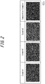
- FIG. 2 presents photographs of the center of the diamond layer surface, observed under the above-described optical microscope in Examples 1 to 3 and Comparative Example 1.
- white portions correspond to diamond particles
- black portions correspond to a base silicon wafer.
- diamond-on-silicon wafers of Examples 7 and 8 were fabricated in accordance with the method described below, and the adhesion of the diamond layer was determined. Specifically, when negatively charged diamond particles were attached to a silicon wafer and when positively charged diamond particles were attached to a silicon wafer, polishing was performed after growing a diamond layer, and whether the diamond layer had peeled or not was determined.
- Example 7 after fabricating a diamond-on-silicon wafer by the same method as in Example 1, mirror polishing was performed to remove a 1 ⁇ m thick layer of the surface of the diamond layer by chemical mechanical polishing (CMP). That is, Example 7 is an experimental example in which diamond particles formed by detonation were immersed in a hydrogen peroxide aqueous solution to terminate diamond particles by carboxyl groups (COOH) thereby negatively charging the diamond particles.
- CMP chemical mechanical polishing
- Example 8 a diamond-on-silicon wafer was prepared by the same method as in Example 1, except that the diamond particles were positively charged and the surface of the diamond layer was then mirror polished in the same manner as in Example 7.
- diamond particles may be terminated by hydrogen or amino groups; for example, a method of performing plasma treatment in a hydrogen atmosphere or a method of performing plasma treatment in an ammonia atmosphere can be used.
- diamond particles formed by detonation were subjected to plasma treatment in an ammonia atmosphere to terminate the diamond particles by amino groups (NH 2 ), thus the diamond particles were positively charged.
- Example 8 in which the diamond particles were positively charged, the surface of the diamond layer peeled, whereas in Example 7, in which the diamond particles were negatively charged, peeling of the surface of the diamond layer did not occur.
- the Coulomb force between the positively charged natural oxide layer sitting on the surface of the silicon wafer and the negatively charged diamond particles is assumed to have improved the adhesion of the diamond layer.
- a diamond-on-silicon wafer in which the particle size of diamond particles in a diamond layer is reduced is obtained.
Landscapes
- Chemical & Material Sciences (AREA)
- Engineering & Computer Science (AREA)
- Materials Engineering (AREA)
- Metallurgy (AREA)
- Organic Chemistry (AREA)
- Chemical Kinetics & Catalysis (AREA)
- General Chemical & Material Sciences (AREA)
- Mechanical Engineering (AREA)
- Crystallography & Structural Chemistry (AREA)
- Inorganic Chemistry (AREA)
- Crystals, And After-Treatments Of Crystals (AREA)
- Chemical Vapour Deposition (AREA)
Abstract
Description
- This disclosure relates to a method of producing a diamond-on-silicon wafer in which a diamond layer is formed on a silicon wafer and a diamond-on-silicon wafer.
- Since diamond has a wide band gap, diamond-on-silicon wafers, in which a diamond layer is formed on a silicon wafer, are widely used as a wide band gap semiconductor suitable for gas sensing devices, temperature sensing devices, radiation/infrared radiation detecting devices, etc.
- As a typical method of producing a diamond-on-silicon wafer, a technique of attaching diamond particles to a surface of a silicon wafer and growing a diamond layer from the attached diamond particles as nuclei is used. For example,
JP 2005-306617 A - PTL 1:
JP 2005-306617 A - In recent years, with a view to further improving the device characteristics of gas sensing devices, temperature sensing devices, radiation/infrared radiation detecting devices, etc., there is a demand for diamond-on-silicon wafers having diamond particles of reduced particle size in a diamond layer. Further, when a diamond-on silicon wafer is used as a vertical device, the thickness of a diamond layer is required to be 10 µm or more. However, even in the case where the diamond particles attached to a silicon wafer as nuclei for growing a diamond layer are fine particles of 50 nm or less are used as in PTL 1, when the diamond layer is thick, the particle size of the diamond particles in the diamond layer is not reduced, and it was found that when a device is formed in such a diamond layer, leak currents are increased and the device characteristics would be deteriorated.
- To address the above problem, it could be helpful to provide a method of producing a diamond-on silicon wafer in which the particle size of diamond particles in a diamond layer is reduced, and a diamond-on-silicon wafer.
- We diligently studied to solve the above problem and found that the above leak currents would increase when the particle size of the diamond particles in the diamond layer exceeds the gate width (approximately 2 µm) of the device. We further studied to reduce the particle size of diamond particles in a diamond layer and found a correlation between the oxygen concentration in a silicon wafer and the particle size of the diamond particles in the diamond layer. We also found that when a silicon wafer having an oxygen concentration of 5 × 10¹⁷ atom/cm3 or less was used as a base substrate of the diamond layer, the maximum particle size of the diamond particles in the diamond layer could be controlled to 2 µm or less even if the diamond layer was thick.
- This disclosure is based on the above findings, and we propose the following features.
- (1) A method of producing a diamond-on-silicon wafer comprising: attaching diamond particles to a surface of a silicon wafer having an oxygen concentration of 5 × 10¹⁷ atom/cm3 or less, and then growing a diamond layer on the silicon wafer by chemical vapor deposition using the diamond particles as nuclei.
- (2) The method of producing a diamond-on-silicon wafer, according to (1) above, wherein either after a diamond particle-containing solution is applied to the surface of the silicon wafer or after the silicon wafer is dipped in a diamond particle-containing solution, heat treatment is performed on the silicon wafer, thereby attaching the diamond particles to the surface of the silicon wafer.
- (3) The method of producing a diamond-on-silicon wafer, according to (2) above, wherein diamond particles in the diamond particle-containing solution are negatively charged.
- (4) The method of producing a diamond-on-silicon wafer, according to (2) or (3) above, wherein an average particle size of the diamond particles in the diamond particle-containing solution is 50 nm or less.
- (5) The method of producing a diamond-on-silicon wafer, according to any one of (2) to (4) above, wherein a temperature of the silicon wafer is less than 100 °C in the heat treatment.
- (6) The method of producing a diamond-on-silicon wafer, according to any one of (1) to (5) above, wherein a maximum particle size of the diamond particles in the diamond layer is 2.0 µm or less.
- (7) The method of producing a diamond-on-silicon wafer, according to any one of (1) to (6) above, wherein a thickness of the diamond layer is 10 µm or more.
- (8) The method of producing a diamond-on-silicon wafer, according to any one of (1) to (7) above, wherein a resistivity of the silicon wafer is 1000 Ω·cm or more.
- (9) A diamond-on-silicon wafer comprising a silicon wafer having an oxygen concentration of 5 × 10¹⁷ atom/cm3 or less and a diamond layer formed on the silicon wafer,
wherein a maximum particle size of diamond particles in the diamond layer is 2.0 µm or less. - (10) The diamond-on-silicon wafer according to (9) above, wherein a thickness of the diamond layer is 10 µm or more.
- (11) The diamond-on-silicon wafer according to (9) or (10) above, wherein a resistivity of the silicon wafer is 1000 Ω·cm or more.
- According to this disclosure, a diamond-on-silicon wafer in which the particle size of diamond particles in a diamond layer is reduced can be obtained.
- In the accompanying drawings:
-
FIGS. 1A to 1D are schematic cross-sectional views illustrating a method of producing a diamond-on-silicon wafer 100 of one embodiment; -
FIG. 2 presents photographs taken by optical microscopy on a surface of a diamond layer in Examples 1 to 3 and Comparative Example 1; and -
FIG. 3 presents photographs depicting cases where peeling of a diamond layer was observed and not observed in Examples 7 and 8. - An embodiment of this disclosure will now be described with reference to the drawings. Note that in
FIG. 1 , the thickness of a diamond particle coatedlayer 12, the particle size ofdiamond particles 14, and the thickness of adiamond layer 16 are exaggerated relative to asilicon wafer 10 for the sake of explanation; accordingly, the ratio between the dimensions does not conform to the actual ratio. - One embodiment of a diamond-on-silicon wafer is depicted in
FIGS. 1A to 1D . - Referring to
FIG. 1 , a method of producing a diamond-on-silicon wafer 100 according to one embodiment is described. First, a silicon wafer 10 having an oxygen concentration of 5 × 10¹⁷ atom/cm3 or less is prepared (FIG. 1(A) ). Next, a diamond particle-containing solution is applied to the surface of the silicon wafer 10 (FIGS. 1A and 1B ). Thus, the diamond particle coatedlayer 12 is formed on the silicon wafer 10 (FIG. 1B ). Next, thesilicon wafer 10 is subjected to heat treatment thereby evaporating the solvent in the diamond particle coatedlayer 12 and strengthening the bond between the surface of thesilicon wafer 10 anddiamond particles 14; thus, thediamond particles 14 are attached to the surface of the silicon wafer 10 (FIGS. 1B and 1C ). Next, adiamond layer 16 is grown on thesilicon wafer 10 by CVD using the attacheddiamond particles 14 as nuclei (FIGS. 1C and ID). In this manner, a diamond-on-silicon wafer 100 is fabricated. The steps of this embodiment will now be described in detail. - Referring to
FIG. 1A , the silicon wafer 10 having an oxygen concentration of 5 × 10¹⁷ atom/cm3 or less is prepared. The "oxygen concentration of the silicon wafer" herein means the mean value of the oxygen concentrations in the thickness direction of thesilicon wafer 10, measured by FT-IR spectroscopy (Old ASTM F121-1979). As will be described in detail, when such a silicon wafer having a low oxygen concentration is used, the out diffusion of oxygen in thesilicon wafer 10 to thediamond layer 16 during the growth of thediamond layer 16 depicted inFIGS. 1C and 1D is suppressed, thus the maximum particle size of the diamond particles in thediamond layer 16 can be controlled to 2.0 µm or less. The thickness of thesilicon wafer 10 may be set depending on the thickness of thediamond layer 16 to be formed. Specifically, since the warpage of the diamond-on-silicon wafer 100 is more significant when thediamond layer 16 is thicker, thesilicon wafer 10 is preferably thick with a view to preventing the warpage. In particular, the thickness of thesilicon wafer 10 is preferably 280 µm or more and 10 cm or less. - Further, the resistivity of the
silicon wafer 10 is preferably 1000 Ω·cm or more. Such a silicon wafer having high resistivity contains few impurities serving as carriers, such as boron and phosphorus, which prevents those impurities from being out-diffused to thediamond layer 16 during the growth of thediamond layer 16. Consequently, the resistance variation in thediamond layer 16 can be prevented. - Next, referring to
FIGS. 1A and 1B , the diamond particle-containing solution is applied to the surface of thesilicon wafer 10 thereby forming a diamond particle coatedlayer 12. Preferred conditions for forming the diamond particle coatedlayer 12 will be described in detail below. - The average particle size of the diamond particles contained in the diamond particle-containing solution is preferably 1 nm or more and 50 nm or less. When the average particle size is 1 nm or more, the
diamond particles 14 can be prevented from being flicked off the surface of thesilicon wafer 10 by the sputtering effect, in early stages of growing of thediamond layer 16. When the average particle size is 50 nm or less, the maximum particle size of the diamond particles in thediamond layer 16 can be 2.0 µm or less even when the thickness of thediamond layer 16 is 10 µm or more. Such diamond particles can be suitably produced from graphite by a known method such as detonation, implosion, or pulverization. Note that "the average particle size of the diamond particles contained in the diamond particle-containing solution" is calculated based on JIS 8819-2, and means the average particle size calculated on the assumption that the size distribution found using a known laser diffraction particle size analyzer conforms to the normal distribution. - Before being coated with the diamond particle-containing solution, the
silicon wafer 10 is typically pickled using, for example, hydrofluoric acid to remove metal impurities deposited on its surface. The surface of thepickled silicon wafer 10 is a repellent surface, and since the repellent surface is active, the particles easily adhere. Therefore, thepickled silicon wafer 10 is preferably washed with pure water or the like to make the surface of thesilicon wafer 10 to have a hydrophilic surface on which a natural oxide layer is formed. Alternatively, thepickled silicon wafer 10 is preferably left in a clean room for a long time to form a natural oxide layer on the surface of thesilicon wafer 10. Thus, the particles can be prevented from being attached to the surface of thesilicon wafer 10. At this point, positive fixed charges are generated in the natural oxide layer. Accordingly, when the diamond particle-containing solution containing negatively charged diamond particles is applied to the surface of the positively charged natural oxide layer, thesilicon wafer 10 and thediamond particles 14 are firmly bonded together due to the Coulomb attraction. This contributes to the improvement in the adhesion of thediamond layer 16 to thesilicon wafer 10. Such negatively charged diamond particles can be obtained by performing oxidation on the diamond particles to terminate the diamond particles by carboxyl groups or ketone groups. Examples of the oxidation process include methods in which diamond particles are oxidized by heat and methods in which diamond particles are immersed in an ozone solution, a nitric acid solution, a hydrogen peroxide aqueous solution, or a perchloric acid solution. - Examples of a solvent for the diamond particle-containing solution include, in addition to water, organic solvents such as methanol, ethanol, 2-propanol, and toluene. One of these solvents can be used alone or two or more of them can be used in combination.
- The content of the diamond particles in the diamond particle-containing solution is preferably 0.03 % by mass or more and 10 % by mass or less with respect to the entire diamond particle-containing solution. When the content is 0.03 % by mass or more, the
diamond particles 14 can be attached to the surface of thesilicon wafer 10 to be uniform in the wafer surface by heat treatment illustrated inFIGS. 1B and 1C and can be used as growth nuclei. When the content is 10 % by mass or less, the attacheddiamond particles 14 can suppress the abnormal growth of thediamond layer 16 depicted inFIGS. 1C and 1D in the growth process. - In view of improving the adhesion between the
diamond particles 14 and thesilicon wafer 10, the diamond particle-containing solution is preferably in the form of a gel. Alternatively, a thickener may be contained in the diamond particle-containing solution. Examples of the thickener include agar, carrageenan, xanthan gum, gellan gum, guar gum, polyvinyl alcohol, polyacrylate-based thickeners, water-soluble celluloses, and polyethylene oxide. One or more of them can be used. When the thickener is contained, the pH of the diamond particle-containing solution is preferably in the range of 6 to 8. - The diamond particle-containing solution may be prepared by mixing and stirring diamond particles in the above solvent so that the diamond particles are dispersed in the solvent. The stirring speed is preferably 500 rpm to 3000 rpm, and the steering time is preferably 10 minutes to 1 hour.
- The diamond particle-containing solution prepared as described above is applied to the surface of the silicon wafer 10 (
FIGS. 1A and 1B ). Here, as a method for applying the diamond particle-containing solution, for example, a known spin coating method can be used. Spin coating allows the diamond particle-containing solution to be uniformly applied to only one of the surfaces of the wafer that is intended to be coated with the diamond particles. - Next, referring to
FIGS. 1B and 1C , heat treatment is performed on thesilicon wafer 10. This evaporates the solvent in the diamond particle coatedlayer 12, so that thediamond particles 14 are attached to the surface of the silicon wafer 10 (FIG. 1C ). Performing heat treatment can increase the adhesion between thediamond particles 14 and thesilicon wafer 10. The temperature of the wafer during heat treatment is preferably less than 100 °C, more preferably 30 °C or more and 80 °C or less. When the temperature is 100 °C or more, bubbles are formed during the boiling of the diamond particle-containing solution, thus the diamond particles would not be attached to part of thesupport substrate 10. If there is a portion where the diamond particles are not attached, peeling of thediamond layer 16 would be initiated from the portion. When the temperature is less than 30 °C, the bond between thesilicon wafer 10 and thediamond particles 14 is weak; thus, thediamond particles 14 are flicked off due to the sputtering effect during the growth of thediamond layer 16 by CVD. This would make it difficult to grow a uniform diamond layer. Further, the heat treatment time is preferably 1 min to 30 min. As a heat treatment apparatus, a known heat treatment apparatus can be used; for example, heat treatment can be performed by placing thesilicon wafer 10 on a heated hot plate. - Next, referring to
FIGS. 1C and ID, thediamond layer 16 is grown on thesilicon wafer 10 by a CVD process under typical conditions using as growth nuclei thediamond particles 14 attached to the surface of thesilicon wafer 10. For the CVD process, plasma-enhanced CVD, hot-filament CVD, etc. can be suitably used. - When plasma-enhanced CVD is used, for example, the
diamond layer 16 is grown at a wafer temperature of 700 °C to 1300 °C by introducing a source gas such as methane into a chamber using hydrogen as a carrier gas. In terms of further improving the uniformity of the thickness of thediamond layer 16, microwave plasma-assisted CVD is preferably used. Microwave plasma-assisted CVD is a method in which a source gas such as methane is digested by microwaves to form plasma in a plasma chamber and the source gas forming a plasma is delivered to theheated silicon wafer 10 thereby growing thediamond layer 16. Here, the pressure in the plasma chamber, the output of the microwaves, and the temperature of the wafer are preferably set as follows. The pressure in the plasma chamber is preferably 10 Torr to 1000 Torr, more preferably 80 Torr to 300 Torr. The output of the microwaves is preferably 0.1 kW to 100 kW, more preferably 1 kW to 10 kW. The temperature of the wafer is preferably 700 °C to 1300 °C, more preferably 900 °C to 1200 °C. - When hot-filament CVD is used, carbon radicals are generated from a hydrocarbon-based source gas such as methane using a filament made of tungsten, tantalum, rhenium, molybdenum, iridium, or the like at a filament temperature of approximately 1900 °C to 2300 °C. The carbon radicals are directed to the
heated silicon wafer 10 thereby growing thediamond layer 16. Hot-filament CVD can easily be applied to larger diameter wafers. Here, the pressure in the chamber, the distance between the filament and thesilicon wafer 10, and the temperature of the wafer are preferably set as follows. The pressure in the chamber is preferably 10 Torr to 1000 Torr. The distance between the filament and thesilicon wafer 10 is preferably 5 mm to 20 mm. The temperature of the wafer is preferably 700 °C to 1300 °C. - Note that the thickness of the
diamond layer 16 to be grown can be selected depending on the intended use of the diamond-on-silicon wafer 100. For example, when thediamond layer 16 is used as an active layer for forming a device in the lateral direction (horizontal direction) for example as in high frequency devices, a diamond layer having a thickness of 0.1 µm to 1 mm is required. On the other hand, when thediamond layer 16 is used as an active layer for forming a device in the upright direction (vertical direction) for example as in power devices, a diamond layer having a thickness of 10 µm to 1 mm is required. - A feature of this embodiment is that a
silicon wafer 10 of low oxygen with an oxygen concentration of 5.0 × 10¹⁷ atoms/cm3 or less is used as the base substrate of thediamond layer 16. The mechanism of the reduction in the size of the diamond particles in thediamond layer 16 with the use of the silicon wafer of low oxygen is assumed as follows. - When the oxygen concentration of the
silicon wafer 10 exceeds 5 × 10¹⁷ atom/cm3, oxygen diffused out of thesilicon wafer 10 due to heat in the process of the growth of the diamond layer preferentially etches a graphite (sp2 orbital) region with weak binding force, constituting growing diamond particles, thus only a diamond (sp3 orbital) region with high binding force is assumed to rapidly grow. Accordingly, the particle size of the diamond particles is large and the surface of the diamond particles is significantly rough, resulting in large gaps between the diamond particles, thus the density of thediamond layer 16 would be low. On the other hand, since the out diffusion of oxygen is suppressed when a silicon wafer of low oxygen is used, etching of the graphite region is suppressed, so that the diamond region is grown while the graphite region is etched in plasma, thus the rapid growth of the diamond region would be mitigated. Consequently, a closelypacked diamond layer 16 having diamond particles with a maximum particle size of 2.0 µm or less is thought to be obtained. Considering this, a gas which does not contain oxygen is preferably used as a carrier gas used in growing thediamond layer 16 in terms of suppressing etching of the graphite region. - A method of producing a diamond-on-silicon wafer has been described using this embodiment as an example; however, this disclosure is not limited to the above embodiment, and modifications may be made as appropriate without departing from the scope defined by the claims.
- The method of attaching the diamond particles to the surface of the silicon wafer is not limited to the application method, and may be a known method such as a dip coating method or a scratching method. When a dip coating method is used, diamond particles can be attached to the surface of the silicon wafer by performing the above-mentioned heat treatment after the silicon wafer is dipped in the diamond particle-containing solution. In the case of a scratching method, diamond particles are embedded into the surface of the silicon wafer, thus the diamond particles are attached to the surface of the silicon wafer. Examples of the method of embedding the diamond particles include: (1) a method of distributing diamond powder in a dried state on the surface of the silicon wafer and applying a pressing force to the wafer surface, (2) a method of sending a blast of a high speed gas containing diamond particles to the surface of the silicon wafer, (3) a method of placing the silicon wafer in a fluidized bed of diamond particles, and (4) a method of performing ultrasonic cleaning on the silicon wafer in a solution in which diamond particles are distributed. In the scratching method, when variation in the depth of the diamond particles results in a non-uniform thickness of the diamond layer, and when the surface of the silicon wafer is greatly damaged during the embedding of the diamond particles, for example, the smoothness of the surface of the diamond layer would be deteriorated. Therefore, an application method or a dip coating method is preferably used.
- Further, the
silicon wafer 10 may be a (100) wafer. In this case, part of the diamond layer excluding a device region formed in the diamond layer may be removed (etched) to fabricate a device (for example, a CMOS device, a memory device, a CIS device, or an IGBT device) in the silicon wafer, thus the device formed in the diamond layer, and the device formed in the silicon wafer can be made into a System on Chip (SoC). - Referring to FIG. ID, the diamond-on-
silicon wafer 100 obtainable by the above production method will be described. The diamond-on-silicon wafer 100 has thesilicon wafer 10 having an oxygen concentration of 5.0 × 10¹⁷ atoms/cm3 or less, and thediamond layer 16 formed on thesilicon wafer 10. The maximum particle size of diamond particles in thediamond layer 16 is 2.0 mm or less. - The "maximum particle size of the diamond particles in the diamond layer" in this specification is defined as follows. Three regions of a wafer that are 10 µm × 10 µm in size are observed under an optical microscope. The three regions are centered at three points, that is, the center of the wafer and the two intersection points between a wafer diameter and the circumference of a circle having a radius which is 95 % of the radius of the wafer radius, the circle being centered at the wafer center. The maximum particle size of all the diamond particles in those three regions is defined as "maximum particle size of the diamond particles in the diamond layer". Note that "particle size of a diamond particles" refers to the length of the major axis of the diamond particle.
- The thickness of the
silicon wafer 10 is preferably 280 µm or more and 10 cm or less, the resistivity of thesilicon wafer 10 is preferably 1000 Ω·cm or more, and thesilicon wafer 10 is preferably a (100) wafer. Further, when thediamond layer 16 is used as an active layer for forming a device in the lateral direction for example as in high frequency devices, the thickness of the diamond layer is preferably 0.1 µm to 1 mm; when thediamond layer 16 is used as an active layer for forming a device in the upright direction for example as in power devices, the thickness of thediamond layer 16 is preferably 10 µm to 1 mm. For the detailed reasons for these values, refer to the description above. - A diamond-on-silicon wafer has been described using this embodiment as an example; however, this disclosure is not limited to the above embodiment, and modifications may be made as appropriate without departing from the scope defined by the claims.
- In Experiment 1, diamond-on-silicon wafers of Examples 1 to 6, and Comparative Examples 1 and 2 were fabricated in accordance with the method described below, and the density of the diamond layer was determined.
- Through the steps depicted in
FIGS. 1A to ID, a diamond-on-silicon wafer was fabricated. - First, a silicon wafer having a diameter of 2 in, a thickness of 3 mm, a (100) crystallographic plane, a resistivity of 1000 Ω·cm, and an oxygen concentration (ASTM F121-1979) of 5.0 × 10¹⁷ atoms/cm3 was prepared by cutting a silicon single crystal ingot grown by the magnetic Czochralski (MCZ) process (
FIG. 1A ). - Next, as diamond particles, diamond particles having an average particle size of 4 nm, produced by detonation were used. The diamond particles were immersed in a hydrogen peroxide aqueous solution to be terminated by carboxyl groups (COOH), thus the diamond particles were negatively charged. Next, a diamond particle-containing solution was prepared by mixing and stirring the diamond particles in a solvent (H2O) such that the concentration of the diamond particles with respect to the entire solution was 0.1 % by mass. The stirring speed was 1100 rpm, the stirring time was 50 min, and the temperature of the diamond particle-containing solution during the stirring was 25 °C. Subsequently, the silicon wafer was cleaned with pure water, and the diamond particle-containing solution was applied by spin coating to a surface of the silicon wafer on which a natural oxide layer was formed; thus, a diamond particle coated layer was formed on the silicon wafer (
FIGS. 1A and 1B ). - Next, the silicon wafer was placed on a hot plate heated to 80 °C, for 3 minutes to perform heat treatment for strengthening the bond between the silicon wafer and the diamond particles; thus, the diamond particles were attached to the surface of the silicon wafer (
FIGS. 1B and 1C ). - Next, a diamond layer with a thickness of 10 µm was grown on the silicon wafer by the above-described microwave plasma-assisted CVD using hydrogen as a carrier gas, methane as a source gas, and the diamond particles attached to the silicon wafer as growth nuclei (
FIGS. 1C and ID). In the growth of the diamond layer, the pressure in the plasma chamber was 135 Torr, the output of the microwaves was 5 kW, the wafer temperature was 1050 °C, and the growth time was 2 h. Thus, a diamond-on-silicon wafer was obtained. - In Example 2, a diamond-on-silicon wafer was produced in the same manner as in Example 1, except that a silicon wafer having an oxygen concentration of 2 × 10¹⁷ atom/cm3, prepared by the MCZ process was used.
- In Example 3, a diamond-on-silicon wafer was produced in the same manner as in Example 1, except that a silicon wafer having an oxygen concentration of 6 × 10¹⁶ atom/cm3, prepared by the floating zone (FZ) process was used.
- In Example 4, a diamond-on-silicon wafer was produced in the same manner as in Example 1, except that the thickness of the diamond layer was 1000 µm.
- In Example 5, a diamond-on-silicon wafer was produced in the same manner as in Example 2, except that the thickness of the diamond layer was 1000 µm.
- In Example 6, a diamond-on-silicon wafer was produced in the same manner as in Example 3, except that the thickness of the diamond layer was 1000 µm.
- In Comparative Example 1, a diamond-on-silicon wafer was produced in the same manner as in Example 1, except that a silicon wafer having an oxygen concentration of 1 × 10¹⁸ atom/cm3 was used.
- In Comparative Example 2, a diamond-on-silicon wafer was produced in same manner as in Comparative Example 1, except that the thickness of the diamond layer was 1000 µm.
- In each of Examples and Comparative Examples, the maximum particle size of the diamond particles in the diamond layer was found by the above-mentioned method, and the density of the diamond layer was determined. The measurement results are given in Table 1. Further,
FIG. 2 presents photographs of the center of the diamond layer surface, observed under the above-described optical microscope in Examples 1 to 3 and Comparative Example 1. Here, inFIG. 2 , white portions correspond to diamond particles, and black portions correspond to a base silicon wafer.Table 1 Sample preparation conditions Evaluation results Oxygen concentration of Si wafer (atoms/cm3) Thickness of Diamond layer (µm) Maximum particle size of Diamond particles in Diamond layer (µm) Example 1 5 × 10¹⁷ 10 1.8 Example 2 2 × 10¹⁷ 10 1.5 Example 3 6 × 10¹⁶ 10 1.2 Example 4 5 × 10¹⁷ 1000 1.9 Example 5 2 × 10¹⁷ 1000 1.7 Example 6 6 × 10¹⁶ 1000 1.4 Comparative Example 1 1 × 10¹⁸ 10 3.0 Comparative Example 2 1 × 10¹⁸ 1000 3.9 - In Comparative Examples 1 and 2, in which a silicon wafer having an oxygen concentration exceeding 5 × 10¹⁷ atom/cm3 was used, the maximum particle size of the diamond particles in the diamond layer exceeded 2.0 µm, whereas in each of Examples 1 to 6, in which a silicon wafer having an oxygen concentration of 5 × 10¹⁷ atom/cm3 or less was used, the maximum particle size of the diamond particles in the diamond layer was 2.0 µm or less. Thus, denser diamond layers were obtained in Examples 1 to 6 as compared with Comparative Examples 1 and 2. The use of a low oxygen silicon wafer with an oxygen concentration of 5 × 10¹⁷ atom/cm3 or less is considered to have suppressed the out diffusion of oxygen to the diamond layer from the silicon wafer.
- In Experiment 2, diamond-on-silicon wafers of Examples 7 and 8 were fabricated in accordance with the method described below, and the adhesion of the diamond layer was determined. Specifically, when negatively charged diamond particles were attached to a silicon wafer and when positively charged diamond particles were attached to a silicon wafer, polishing was performed after growing a diamond layer, and whether the diamond layer had peeled or not was determined.
- In Example 7, after fabricating a diamond-on-silicon wafer by the same method as in Example 1, mirror polishing was performed to remove a 1 µm thick layer of the surface of the diamond layer by chemical mechanical polishing (CMP). That is, Example 7 is an experimental example in which diamond particles formed by detonation were immersed in a hydrogen peroxide aqueous solution to terminate diamond particles by carboxyl groups (COOH) thereby negatively charging the diamond particles.
- In Example 8, a diamond-on-silicon wafer was prepared by the same method as in Example 1, except that the diamond particles were positively charged and the surface of the diamond layer was then mirror polished in the same manner as in Example 7. In order to positively charge diamond particles, diamond particles may be terminated by hydrogen or amino groups; for example, a method of performing plasma treatment in a hydrogen atmosphere or a method of performing plasma treatment in an ammonia atmosphere can be used. In Example 8, diamond particles formed by detonation were subjected to plasma treatment in an ammonia atmosphere to terminate the diamond particles by amino groups (NH2), thus the diamond particles were positively charged.
- In Examples 7 and 8, whether or not peeling of the diamond layer was found in the surface of the diamond layer was determined by visual observation, thereby determining the adhesion. The observation results are given in
FIG. 3 . - In Example 8, in which the diamond particles were positively charged, the surface of the diamond layer peeled, whereas in Example 7, in which the diamond particles were negatively charged, peeling of the surface of the diamond layer did not occur. The Coulomb force between the positively charged natural oxide layer sitting on the surface of the silicon wafer and the negatively charged diamond particles is assumed to have improved the adhesion of the diamond layer.
- According to this disclosure, a diamond-on-silicon wafer in which the particle size of diamond particles in a diamond layer is reduced is obtained.
-
- 100:
- Diamond-on-silicon wafer
- 10:
- Silicon wafer
- 12:
- Diamond particle coated layer
- 14:
- Diamond particle
- 16:
- Diamond layer
Claims (11)
- A method of producing a diamond-on-silicon wafer comprising:attaching diamond particles to a surface of a silicon wafer having an oxygen concentration of 5 × 10¹⁷ atom/cm3 or less, andthen growing a diamond layer on the silicon wafer by chemical vapor deposition using the diamond particles as nuclei.
- The method of producing a diamond-on-silicon wafer, according to Claim 1, wherein either after a diamond particle-containing solution is applied to the surface of the silicon wafer or after the silicon wafer is dipped in a diamond particle-containing solution, heat treatment is performed on the silicon wafer, thereby attaching the diamond particles to the surface of the silicon wafer.
- The method of producing a diamond-on-silicon wafer, according to Claim 2, wherein diamond particles in the diamond particle-containing solution are negatively charged.
- The method of producing a diamond-on-silicon wafer, according to Claim 2 or 3, wherein an average particle size of the diamond particles in the diamond particle-containing solution is 50 nm or less.
- The method of producing a diamond-on-silicon wafer, according to any one of Claims 2 to 4, wherein a temperature of the silicon wafer is less than 100 °C in the heat treatment.
- The method of producing a diamond-on-silicon wafer, according to any one of Claims 1 to 5, wherein a maximum particle size of the diamond particles in the diamond layer is 2.0 µm or less.
- The method of producing a diamond-on-silicon wafer, according to any one of Claims 1 to 6, wherein a thickness of the diamond layer is 10 µm or more.
- The method of producing a diamond-on-silicon wafer, according to any one of Claims 1 to 7, wherein a resistivity of the silicon wafer is 1000 Ω·cm or more.
- A diamond-on-silicon wafer comprising a silicon wafer having an oxygen concentration of 5 × 10¹⁷ atom/cm3 or less and a diamond layer formed on the silicon wafer,
wherein a maximum particle size of diamond particles in the diamond layer is 2.0 µm or less. - The diamond-on-silicon wafer according to Claim 9, wherein a thickness of the diamond layer is 10 µm or more.
- The diamond-on-silicon wafer according to Claim 9 or 10, wherein a resistivity of the silicon wafer is 1000 Ω·cm or more.
Applications Claiming Priority (2)
| Application Number | Priority Date | Filing Date | Title |
|---|---|---|---|
| JP2017141860A JP6825509B2 (en) | 2017-07-21 | 2017-07-21 | Manufacturing method of diamond laminated silicon wafer and diamond laminated silicon wafer |
| PCT/JP2018/026715 WO2019017330A1 (en) | 2017-07-21 | 2018-07-17 | Method for producing diamond laminated silicon wafer, and diamond laminated silicon wafer |
Publications (3)
| Publication Number | Publication Date |
|---|---|
| EP3656896A1 true EP3656896A1 (en) | 2020-05-27 |
| EP3656896A4 EP3656896A4 (en) | 2021-03-31 |
| EP3656896B1 EP3656896B1 (en) | 2025-07-02 |
Family
ID=65015107
Family Applications (1)
| Application Number | Title | Priority Date | Filing Date |
|---|---|---|---|
| EP18835867.5A Active EP3656896B1 (en) | 2017-07-21 | 2018-07-17 | Method for producing diamond laminated silicon wafer, and diamond laminated silicon wafer |
Country Status (4)
| Country | Link |
|---|---|
| EP (1) | EP3656896B1 (en) |
| JP (1) | JP6825509B2 (en) |
| CN (1) | CN111051579B (en) |
| WO (1) | WO2019017330A1 (en) |
Cited By (1)
| Publication number | Priority date | Publication date | Assignee | Title |
|---|---|---|---|---|
| DE112019006310B4 (en) | 2018-12-19 | 2026-03-12 | Sumco Corporation | METHOD FOR PRODUCING A FREESTANDING POLYCRYSTALLINE DIAMOND SUBSTRATE |
Families Citing this family (2)
| Publication number | Priority date | Publication date | Assignee | Title |
|---|---|---|---|---|
| JP7571390B2 (en) * | 2020-05-07 | 2024-10-23 | 富士通株式会社 | Semiconductor Device |
| CN114032525B (en) * | 2021-11-04 | 2023-09-12 | 西南科技大学 | Diamond-multilayer graphene composite cathode material and preparation method thereof |
Family Cites Families (7)
| Publication number | Priority date | Publication date | Assignee | Title |
|---|---|---|---|---|
| JPH0815160B2 (en) * | 1991-03-29 | 1996-02-14 | 株式会社神戸製鋼所 | Diamond Schottky gate type field effect transistor |
| JPH1081589A (en) * | 1996-06-12 | 1998-03-31 | Matsushita Electric Ind Co Ltd | Diamond film and method of manufacturing the same |
| EP0844319A4 (en) * | 1996-06-12 | 2001-09-05 | Matsushita Electric Industrial Co Ltd | DIAMOND FILM AND MANUFACTURING METHOD |
| JP2005306617A (en) | 2004-04-16 | 2005-11-04 | Matsushita Electric Ind Co Ltd | Diamond thin film and manufacturing method thereof |
| JP2009091234A (en) * | 2007-09-18 | 2009-04-30 | Tokyo Univ Of Science | Substrate on which conductive diamond film is formed and method for manufacturing substrate on which conductive diamond film is formed |
| JP4984263B2 (en) * | 2008-09-17 | 2012-07-25 | 住友電工ハードメタル株式会社 | Diamond film and manufacturing method thereof |
| JP5510256B2 (en) * | 2010-10-06 | 2014-06-04 | 株式会社Sumco | Silicon wafer manufacturing method |
-
2017
- 2017-07-21 JP JP2017141860A patent/JP6825509B2/en active Active
-
2018
- 2018-07-17 CN CN201880048894.8A patent/CN111051579B/en active Active
- 2018-07-17 WO PCT/JP2018/026715 patent/WO2019017330A1/en not_active Ceased
- 2018-07-17 EP EP18835867.5A patent/EP3656896B1/en active Active
Cited By (1)
| Publication number | Priority date | Publication date | Assignee | Title |
|---|---|---|---|---|
| DE112019006310B4 (en) | 2018-12-19 | 2026-03-12 | Sumco Corporation | METHOD FOR PRODUCING A FREESTANDING POLYCRYSTALLINE DIAMOND SUBSTRATE |
Also Published As
| Publication number | Publication date |
|---|---|
| EP3656896A4 (en) | 2021-03-31 |
| JP6825509B2 (en) | 2021-02-03 |
| WO2019017330A1 (en) | 2019-01-24 |
| CN111051579A (en) | 2020-04-21 |
| CN111051579B (en) | 2021-12-28 |
| EP3656896B1 (en) | 2025-07-02 |
| JP2019019044A (en) | 2019-02-07 |
Similar Documents
| Publication | Publication Date | Title |
|---|---|---|
| JP7115297B2 (en) | Polycrystalline diamond free-standing substrate and its manufacturing method | |
| US10832937B1 (en) | High resistivity silicon-on-insulator substrate having enhanced charge trapping efficiency | |
| US11183420B2 (en) | High resistivity silicon-on-insulator wafer manufacturing method for reducing substrate loss | |
| TWI711067B (en) | Method of depositing charge trapping polycrystalline silicon films on silicon substrates with controllable film stress | |
| TWI709197B (en) | A method of manufacturing high resistivity semiconductor-on-insulator wafers with charge trapping layers | |
| TWI626690B (en) | Manufacturing method of smoothing a semiconductor surface | |
| JP7172556B2 (en) | Method for manufacturing polycrystalline diamond free-standing substrate | |
| EP2879176B1 (en) | Method for producing hybrid substrates, and hybrid substrate | |
| EP3352197A1 (en) | METHOD FOR PRODUCING SiC COMPOSITE SUBSTRATE | |
| EP3656896B1 (en) | Method for producing diamond laminated silicon wafer, and diamond laminated silicon wafer | |
| TW201133615A (en) | Wafer adhesion method | |
| TW202503979A (en) | Methods of manufacturing semiconductor-on-insulator wafers having charge trapping layers with controlled stress | |
| TWI363388B (en) | ||
| JP6772995B2 (en) | Manufacturing method of SOI wafer and SOI wafer | |
| CN117038572A (en) | Method for fabricating semiconductor-on-insulator structures | |
| CN114672879B (en) | Polycrystalline diamond self-supporting substrate and preparation method thereof | |
| JP7238753B2 (en) | Bonded wafer and its manufacturing method | |
| JP7600973B2 (en) | Stacked wafer and manufacturing method thereof | |
| EP4609420A1 (en) | Method for producing a high-resistivity semiconductor stack and associated stack |
Legal Events
| Date | Code | Title | Description |
|---|---|---|---|
| STAA | Information on the status of an ep patent application or granted ep patent |
Free format text: STATUS: THE INTERNATIONAL PUBLICATION HAS BEEN MADE |
|
| PUAI | Public reference made under article 153(3) epc to a published international application that has entered the european phase |
Free format text: ORIGINAL CODE: 0009012 |
|
| STAA | Information on the status of an ep patent application or granted ep patent |
Free format text: STATUS: REQUEST FOR EXAMINATION WAS MADE |
|
| 17P | Request for examination filed |
Effective date: 20191219 |
|
| AK | Designated contracting states |
Kind code of ref document: A1 Designated state(s): AL AT BE BG CH CY CZ DE DK EE ES FI FR GB GR HR HU IE IS IT LI LT LU LV MC MK MT NL NO PL PT RO RS SE SI SK SM TR |
|
| AX | Request for extension of the european patent |
Extension state: BA ME |
|
| DAV | Request for validation of the european patent (deleted) | ||
| DAX | Request for extension of the european patent (deleted) | ||
| A4 | Supplementary search report drawn up and despatched |
Effective date: 20210302 |
|
| RIC1 | Information provided on ipc code assigned before grant |
Ipc: C30B 29/04 20060101AFI20210224BHEP Ipc: C23C 16/27 20060101ALI20210224BHEP Ipc: H01L 21/205 20060101ALI20210224BHEP Ipc: C30B 25/18 20060101ALI20210224BHEP Ipc: H01L 21/02 20060101ALI20210224BHEP |
|
| STAA | Information on the status of an ep patent application or granted ep patent |
Free format text: STATUS: EXAMINATION IS IN PROGRESS |
|
| 17Q | First examination report despatched |
Effective date: 20240506 |
|
| GRAP | Despatch of communication of intention to grant a patent |
Free format text: ORIGINAL CODE: EPIDOSNIGR1 |
|
| STAA | Information on the status of an ep patent application or granted ep patent |
Free format text: STATUS: GRANT OF PATENT IS INTENDED |
|
| RIC1 | Information provided on ipc code assigned before grant |
Ipc: C23C 16/02 20060101ALI20250129BHEP Ipc: C23C 16/01 20060101ALI20250129BHEP Ipc: H01L 21/02 20060101ALI20250129BHEP Ipc: H01L 21/205 20060101ALI20250129BHEP Ipc: C30B 25/18 20060101ALI20250129BHEP Ipc: C23C 16/27 20060101ALI20250129BHEP Ipc: C30B 29/04 20060101AFI20250129BHEP |
|
| INTG | Intention to grant announced |
Effective date: 20250224 |
|
| RIN1 | Information on inventor provided before grant (corrected) |
Inventor name: KOGA, YOSHIHIRO |
|
| GRAS | Grant fee paid |
Free format text: ORIGINAL CODE: EPIDOSNIGR3 |
|
| GRAA | (expected) grant |
Free format text: ORIGINAL CODE: 0009210 |
|
| STAA | Information on the status of an ep patent application or granted ep patent |
Free format text: STATUS: THE PATENT HAS BEEN GRANTED |
|
| AK | Designated contracting states |
Kind code of ref document: B1 Designated state(s): AL AT BE BG CH CY CZ DE DK EE ES FI FR GB GR HR HU IE IS IT LI LT LU LV MC MK MT NL NO PL PT RO RS SE SI SK SM TR |
|
| REG | Reference to a national code |
Ref country code: GB Ref legal event code: FG4D |
|
| REG | Reference to a national code |
Ref country code: CH Ref legal event code: EP |
|
| REG | Reference to a national code |
Ref country code: DE Ref legal event code: R096 Ref document number: 602018083272 Country of ref document: DE |
|
| REG | Reference to a national code |
Ref country code: IE Ref legal event code: FG4D |
|
| PGFP | Annual fee paid to national office [announced via postgrant information from national office to epo] |
Ref country code: DE Payment date: 20250626 Year of fee payment: 8 |
|
| PGFP | Annual fee paid to national office [announced via postgrant information from national office to epo] |
Ref country code: CH Payment date: 20250801 Year of fee payment: 8 |
|
| REG | Reference to a national code |
Ref country code: NL Ref legal event code: MP Effective date: 20250702 |
|
| PG25 | Lapsed in a contracting state [announced via postgrant information from national office to epo] |
Ref country code: PT Free format text: LAPSE BECAUSE OF FAILURE TO SUBMIT A TRANSLATION OF THE DESCRIPTION OR TO PAY THE FEE WITHIN THE PRESCRIBED TIME-LIMIT Effective date: 20251103 |
|
| PG25 | Lapsed in a contracting state [announced via postgrant information from national office to epo] |
Ref country code: NL Free format text: LAPSE BECAUSE OF FAILURE TO SUBMIT A TRANSLATION OF THE DESCRIPTION OR TO PAY THE FEE WITHIN THE PRESCRIBED TIME-LIMIT Effective date: 20250702 |
|
| REG | Reference to a national code |
Ref country code: AT Ref legal event code: MK05 Ref document number: 1809345 Country of ref document: AT Kind code of ref document: T Effective date: 20250702 |
|
| PG25 | Lapsed in a contracting state [announced via postgrant information from national office to epo] |
Ref country code: IS Free format text: LAPSE BECAUSE OF FAILURE TO SUBMIT A TRANSLATION OF THE DESCRIPTION OR TO PAY THE FEE WITHIN THE PRESCRIBED TIME-LIMIT Effective date: 20251102 |
|
| PG25 | Lapsed in a contracting state [announced via postgrant information from national office to epo] |
Ref country code: NO Free format text: LAPSE BECAUSE OF FAILURE TO SUBMIT A TRANSLATION OF THE DESCRIPTION OR TO PAY THE FEE WITHIN THE PRESCRIBED TIME-LIMIT Effective date: 20251002 |
|
| REG | Reference to a national code |
Ref country code: LT Ref legal event code: MG9D |
|
| PG25 | Lapsed in a contracting state [announced via postgrant information from national office to epo] |
Ref country code: AT Free format text: LAPSE BECAUSE OF FAILURE TO SUBMIT A TRANSLATION OF THE DESCRIPTION OR TO PAY THE FEE WITHIN THE PRESCRIBED TIME-LIMIT Effective date: 20250702 |
|
| PG25 | Lapsed in a contracting state [announced via postgrant information from national office to epo] |
Ref country code: FI Free format text: LAPSE BECAUSE OF FAILURE TO SUBMIT A TRANSLATION OF THE DESCRIPTION OR TO PAY THE FEE WITHIN THE PRESCRIBED TIME-LIMIT Effective date: 20250702 |
|
| PG25 | Lapsed in a contracting state [announced via postgrant information from national office to epo] |
Ref country code: HR Free format text: LAPSE BECAUSE OF FAILURE TO SUBMIT A TRANSLATION OF THE DESCRIPTION OR TO PAY THE FEE WITHIN THE PRESCRIBED TIME-LIMIT Effective date: 20250702 |
|
| PG25 | Lapsed in a contracting state [announced via postgrant information from national office to epo] |
Ref country code: GR Free format text: LAPSE BECAUSE OF FAILURE TO SUBMIT A TRANSLATION OF THE DESCRIPTION OR TO PAY THE FEE WITHIN THE PRESCRIBED TIME-LIMIT Effective date: 20251003 |
|
| PG25 | Lapsed in a contracting state [announced via postgrant information from national office to epo] |
Ref country code: SE Free format text: LAPSE BECAUSE OF FAILURE TO SUBMIT A TRANSLATION OF THE DESCRIPTION OR TO PAY THE FEE WITHIN THE PRESCRIBED TIME-LIMIT Effective date: 20250702 Ref country code: CZ Free format text: LAPSE BECAUSE OF FAILURE TO SUBMIT A TRANSLATION OF THE DESCRIPTION OR TO PAY THE FEE WITHIN THE PRESCRIBED TIME-LIMIT Effective date: 20250702 |
|
| PG25 | Lapsed in a contracting state [announced via postgrant information from national office to epo] |
Ref country code: LV Free format text: LAPSE BECAUSE OF FAILURE TO SUBMIT A TRANSLATION OF THE DESCRIPTION OR TO PAY THE FEE WITHIN THE PRESCRIBED TIME-LIMIT Effective date: 20250702 |
|
| PG25 | Lapsed in a contracting state [announced via postgrant information from national office to epo] |
Ref country code: BG Free format text: LAPSE BECAUSE OF FAILURE TO SUBMIT A TRANSLATION OF THE DESCRIPTION OR TO PAY THE FEE WITHIN THE PRESCRIBED TIME-LIMIT Effective date: 20250702 Ref country code: PL Free format text: LAPSE BECAUSE OF FAILURE TO SUBMIT A TRANSLATION OF THE DESCRIPTION OR TO PAY THE FEE WITHIN THE PRESCRIBED TIME-LIMIT Effective date: 20250702 |
|
| PG25 | Lapsed in a contracting state [announced via postgrant information from national office to epo] |
Ref country code: RS Free format text: LAPSE BECAUSE OF FAILURE TO SUBMIT A TRANSLATION OF THE DESCRIPTION OR TO PAY THE FEE WITHIN THE PRESCRIBED TIME-LIMIT Effective date: 20251002 |
|
| PG25 | Lapsed in a contracting state [announced via postgrant information from national office to epo] |
Ref country code: ES Free format text: LAPSE BECAUSE OF FAILURE TO SUBMIT A TRANSLATION OF THE DESCRIPTION OR TO PAY THE FEE WITHIN THE PRESCRIBED TIME-LIMIT Effective date: 20250702 |
|
| PG25 | Lapsed in a contracting state [announced via postgrant information from national office to epo] |
Ref country code: RO Free format text: LAPSE BECAUSE OF FAILURE TO SUBMIT A TRANSLATION OF THE DESCRIPTION OR TO PAY THE FEE WITHIN THE PRESCRIBED TIME-LIMIT Effective date: 20250702 Ref country code: LU Free format text: LAPSE BECAUSE OF NON-PAYMENT OF DUE FEES Effective date: 20250717 |
|
| REG | Reference to a national code |
Ref country code: BE Ref legal event code: MM Effective date: 20250731 |
|
| PG25 | Lapsed in a contracting state [announced via postgrant information from national office to epo] |
Ref country code: SM Free format text: LAPSE BECAUSE OF FAILURE TO SUBMIT A TRANSLATION OF THE DESCRIPTION OR TO PAY THE FEE WITHIN THE PRESCRIBED TIME-LIMIT Effective date: 20250702 |
|
| PG25 | Lapsed in a contracting state [announced via postgrant information from national office to epo] |
Ref country code: DK Free format text: LAPSE BECAUSE OF FAILURE TO SUBMIT A TRANSLATION OF THE DESCRIPTION OR TO PAY THE FEE WITHIN THE PRESCRIBED TIME-LIMIT Effective date: 20250702 |
|
| PG25 | Lapsed in a contracting state [announced via postgrant information from national office to epo] |
Ref country code: IT Free format text: LAPSE BECAUSE OF FAILURE TO SUBMIT A TRANSLATION OF THE DESCRIPTION OR TO PAY THE FEE WITHIN THE PRESCRIBED TIME-LIMIT Effective date: 20250702 Ref country code: BE Free format text: LAPSE BECAUSE OF NON-PAYMENT OF DUE FEES Effective date: 20250731 |
|
| PG25 | Lapsed in a contracting state [announced via postgrant information from national office to epo] |
Ref country code: SK Free format text: LAPSE BECAUSE OF FAILURE TO SUBMIT A TRANSLATION OF THE DESCRIPTION OR TO PAY THE FEE WITHIN THE PRESCRIBED TIME-LIMIT Effective date: 20250702 Ref country code: EE Free format text: LAPSE BECAUSE OF FAILURE TO SUBMIT A TRANSLATION OF THE DESCRIPTION OR TO PAY THE FEE WITHIN THE PRESCRIBED TIME-LIMIT Effective date: 20250702 |
|
| PLBE | No opposition filed within time limit |
Free format text: ORIGINAL CODE: 0009261 |
|
| STAA | Information on the status of an ep patent application or granted ep patent |
Free format text: STATUS: NO OPPOSITION FILED WITHIN TIME LIMIT |