EP3656057B1 - Current sink with negative voltage tolerance - Google Patents
Current sink with negative voltage tolerance Download PDFInfo
- Publication number
- EP3656057B1 EP3656057B1 EP18835338.7A EP18835338A EP3656057B1 EP 3656057 B1 EP3656057 B1 EP 3656057B1 EP 18835338 A EP18835338 A EP 18835338A EP 3656057 B1 EP3656057 B1 EP 3656057B1
- Authority
- EP
- European Patent Office
- Prior art keywords
- coupled
- gate
- nmos transistor
- control signal
- node
- Prior art date
- Legal status (The legal status is an assumption and is not a legal conclusion. Google has not performed a legal analysis and makes no representation as to the accuracy of the status listed.)
- Active
Links
Images




Classifications
-
- G—PHYSICS
- G05—CONTROLLING; REGULATING
- G05F—SYSTEMS FOR REGULATING ELECTRIC OR MAGNETIC VARIABLES
- G05F3/00—Non-retroactive systems for regulating electric variables by using an uncontrolled element, or an uncontrolled combination of elements, such element or such combination having self-regulating properties
- G05F3/02—Regulating voltage or current
- G05F3/08—Regulating voltage or current wherein the variable is DC
- G05F3/10—Regulating voltage or current wherein the variable is DC using uncontrolled devices with non-linear characteristics
- G05F3/16—Regulating voltage or current wherein the variable is DC using uncontrolled devices with non-linear characteristics being semiconductor devices
- G05F3/20—Regulating voltage or current wherein the variable is DC using uncontrolled devices with non-linear characteristics being semiconductor devices using diode- transistor combinations
- G05F3/26—Current mirrors
- G05F3/262—Current mirrors using field-effect transistors only
-
- B—PERFORMING OPERATIONS; TRANSPORTING
- B60—VEHICLES IN GENERAL
- B60T—VEHICLE BRAKE CONTROL SYSTEMS OR PARTS THEREOF; BRAKE CONTROL SYSTEMS OR PARTS THEREOF, IN GENERAL; ARRANGEMENT OF BRAKING ELEMENTS ON VEHICLES IN GENERAL; PORTABLE DEVICES FOR PREVENTING UNWANTED MOVEMENT OF VEHICLES; VEHICLE MODIFICATIONS TO FACILITATE COOLING OF BRAKES
- B60T8/00—Arrangements for adjusting wheel-braking force to meet varying vehicular or ground-surface conditions, e.g. limiting or varying distribution of braking force
- B60T8/17—Using electrical or electronic regulation means to control braking
- B60T8/172—Determining control parameters used in the regulation, e.g. by calculations involving measured or detected parameters
-
- B—PERFORMING OPERATIONS; TRANSPORTING
- B60—VEHICLES IN GENERAL
- B60T—VEHICLE BRAKE CONTROL SYSTEMS OR PARTS THEREOF; BRAKE CONTROL SYSTEMS OR PARTS THEREOF, IN GENERAL; ARRANGEMENT OF BRAKING ELEMENTS ON VEHICLES IN GENERAL; PORTABLE DEVICES FOR PREVENTING UNWANTED MOVEMENT OF VEHICLES; VEHICLE MODIFICATIONS TO FACILITATE COOLING OF BRAKES
- B60T8/00—Arrangements for adjusting wheel-braking force to meet varying vehicular or ground-surface conditions, e.g. limiting or varying distribution of braking force
- B60T8/17—Using electrical or electronic regulation means to control braking
- B60T8/176—Brake regulation specially adapted to prevent excessive wheel slip during vehicle deceleration, e.g. ABS
- B60T8/1761—Brake regulation specially adapted to prevent excessive wheel slip during vehicle deceleration, e.g. ABS responsive to wheel or brake dynamics, e.g. wheel slip, wheel acceleration or rate of change of brake fluid pressure
- B60T8/17613—Brake regulation specially adapted to prevent excessive wheel slip during vehicle deceleration, e.g. ABS responsive to wheel or brake dynamics, e.g. wheel slip, wheel acceleration or rate of change of brake fluid pressure based on analogue circuits or digital circuits comprised of discrete electronic elements
-
- H—ELECTRICITY
- H03—ELECTRONIC CIRCUITRY
- H03K—PULSE TECHNIQUE
- H03K17/00—Electronic switching or gating, i.e. not by contact-making and –breaking
- H03K17/06—Modifications for ensuring a fully conducting state
- H03K17/063—Modifications for ensuring a fully conducting state in field-effect transistor switches
-
- H—ELECTRICITY
- H03—ELECTRONIC CIRCUITRY
- H03K—PULSE TECHNIQUE
- H03K17/00—Electronic switching or gating, i.e. not by contact-making and –breaking
- H03K17/08—Modifications for protecting switching circuit against overcurrent or overvoltage
- H03K17/082—Modifications for protecting switching circuit against overcurrent or overvoltage by feedback from the output to the control circuit
- H03K17/0822—Modifications for protecting switching circuit against overcurrent or overvoltage by feedback from the output to the control circuit in field-effect transistor switches
-
- H—ELECTRICITY
- H03—ELECTRONIC CIRCUITRY
- H03K—PULSE TECHNIQUE
- H03K17/00—Electronic switching or gating, i.e. not by contact-making and –breaking
- H03K17/16—Modifications for eliminating interference voltages or currents
- H03K17/161—Modifications for eliminating interference voltages or currents in field-effect transistor switches
- H03K17/162—Modifications for eliminating interference voltages or currents in field-effect transistor switches without feedback from the output circuit to the control circuit
-
- H—ELECTRICITY
- H03—ELECTRONIC CIRCUITRY
- H03K—PULSE TECHNIQUE
- H03K17/00—Electronic switching or gating, i.e. not by contact-making and –breaking
- H03K17/51—Electronic switching or gating, i.e. not by contact-making and –breaking characterised by the components used
- H03K17/56—Electronic switching or gating, i.e. not by contact-making and –breaking characterised by the components used by the use, as active elements, of semiconductor devices
- H03K17/687—Electronic switching or gating, i.e. not by contact-making and –breaking characterised by the components used by the use, as active elements, of semiconductor devices the devices being field-effect transistors
-
- H—ELECTRICITY
- H03—ELECTRONIC CIRCUITRY
- H03K—PULSE TECHNIQUE
- H03K17/00—Electronic switching or gating, i.e. not by contact-making and –breaking
- H03K17/06—Modifications for ensuring a fully conducting state
- H03K2017/066—Maximizing the OFF-resistance instead of minimizing the ON-resistance
-
- H—ELECTRICITY
- H03—ELECTRONIC CIRCUITRY
- H03K—PULSE TECHNIQUE
- H03K17/00—Electronic switching or gating, i.e. not by contact-making and –breaking
- H03K17/30—Modifications for providing a predetermined threshold before switching
- H03K2017/307—Modifications for providing a predetermined threshold before switching circuits simulating a diode, e.g. threshold zero
Definitions
- This relates generally to current sinks, and more particularly to a current sink with negative voltage tolerance.
- an actuator In some safety critical situations, such as automotive braking applications, an actuator must not be turned ON inadvertently. This means that the actuator must turn ON only when software initiates a turn ON condition and must remain OFF in all other conditions.
- NMOS N-type metal oxide silicon
- FET field effect transistor
- the OFF condition should be ensured by a strong gate pull down current.
- the pull down current should be active under any phase of operation, have a low overall quiescent current, and be able to operate in a harsh automotive environment that includes fast battery transients and inductive switching that can result in voltage levels of 40V and -25V.
- WO 2015/056042 discloses an IGBT driver module and method therefor.
- EP 2 073 386 relates to a semiconductor output circuit.
- WO 2016/170724 discloses a solid state relay.
- Described embodiments include a circuit that provides a strong gate pull down current using multiple voltage inputs while protecting the circuit from both high and low transient voltages.
- a voltage to drive the pull down circuit can be drawn from the drains of one or more control NMOS power FETs, other sources tied to the battery or to additional voltages available when the ignition is ON. Elements of the circuit are protected from high voltages and negative voltages.
- a current sink circuit is coupled to pull down a gate control node for an N-type metal oxide (NMOS) power field effect transistor (FET) that controls an actuator.
- the current sink circuit includes a first NMOS transistor coupled in series with a second NMOS transistor between the gate control node and a lower rail.
- the first NMOS transistor has a respective gate and source coupled together through a first resistor.
- a control signal generation circuit is coupled to receive at least one voltage input and an ignition signal and is further coupled to provide a first control signal and a second control signal.
- the second control signal is coupled to the gate of the second NMOS transistor.
- a negative voltage blocking circuit is coupled to pass the first control signal from the control signal generation circuit to the gate of the first NMOS transistor and to block a negative voltage on the gate control node from reaching the control signal generation circuit.
- a system-on-chip includes a power supply module coupled to a connector for coupling to a battery.
- Transceivers are coupled to the power supply modules.
- Valve drivers are coupled to respective connectors for connection to a respective actuator.
- Current sink circuits are coupled to pull down a gate control node for a respective N-type metal oxide (NMOS) power field effect transistor (FET) that switches a respective valve driver of the valve drivers and a respective actuator coupled thereto.
- NMOS N-type metal oxide
- One of the current sink circuits includes: a first NMOS transistor coupled in series with a second NMOS transistor between the gate control node and a lower rail, the first NMOS transistor having a respective gate and source coupled together through a first resistor; a control signal generation circuit coupled to receive at least one voltage input and an ignition signal and further coupled to provide a first control signal and a second control signal, the second control signal being coupled to the gate of the second NMOS transistor; and a negative voltage blocking circuit coupled to pass the first control signal from the control signal generation circuit to the gate of the first NMOS transistor and to block a negative voltage on the gate control node from reaching the control signal generation circuit.
- Couple means either an indirect or direct electrical connection unless qualified as in “communicably coupled” which may include wireless connections.
- that connection may be through a direct electrical connection, or through an indirect electrical connection via other devices and connections.
- FIG. 1 depicts an example of a schematic for an actuator control system 100 for an automotive application in which a current sink according to this description can be used.
- Actuator control system 100 includes an NMOS power FET 106 that controls a current between drain 108 and source 110.
- Source 110 is coupled to valve driver 112 that controls specific valves in the vehicle to effect, e.g., braking.
- a control signal CSA is provided to driver 102, which in turn is coupled to provide a control signal on gate control node (GCN) 104 to turn NMOS power FET 106 ON and OFF.
- GCN gate control node
- NMOS power FET 106 must not turn ON unless driven to turn ON by driver 102.
- a gate pull-down circuit 114 is selectively coupled between gate control node 104 and the lower rail by a switch S1 that is controlled by control signal CSB.
- control signals CSA and CSB have opposite logic values. Accordingly, when control signal CSA is high, NMOS power FET 106 is turned ON, control signal CSB is low and opens switch S1. When control signal CSA is low, control signal CSB is high and closes switch S1, pulling down gate control node 104.
- Gate pull-down circuit 114 needs to be active under any phase of operation, yet maintain a low quiescent current from the battery. Gate pull-down circuit 114 must be able to handle fast battery transients and inductive switching and the resulting voltage levels of 40V to -25V.
- FIG. 2 provides a schematic of an example actuator control system 200 that provides somewhat greater detail to describe some of the needs of the specific application.
- Actuator control system 200 includes NMOS power FET 206, which is coupled to gate control node GCN 204, drain 208C and source 210.
- NMOS power FET 206 when turned ON, will supply power to valve driver 212.
- NMOS power FET 206 is one of three switches that are each tied to a separate valve driver, although the other two NMOS power FETs are not shown and are represented only by their respective drains 208A, 208B.
- NMOS power FET 206 and the NMOS power FETs represented by drains 208A, 208B are coupled to be driven by respective drivers 202A, 202B, 202C; greater detail is shown only for driver 202C.
- pulse width modulation (PWM) current source 220 sources current to gate control node 204 when switch S2 is closed and PWM current sink 222 sinks current from gate control node 204 when switch S3 is closed.
- PWM current source 220 and PWM current sink 222 are active to control NMOS power FET 206 when the ignition for the vehicle is turned ON.
- switch S 1 is closed and gate current sink 224 sinks current from GCN 204.
- wake-up detection circuit 214 When a user with an electronic key is near the vehicle, wake-up detection circuit 214 enables several functions in the vehicle; these functions in turn provide an ultra-low current output
- the ultra-low current is provided to a regulator 216, which also acts as a bias generator.
- the wake-up detection circuit 214 and regulator 216 are selectively coupled to charge pump 218 through switch S4.
- Charge pump 218 is further coupled to driver 202 to provide a voltage to PWM current source 220.
- gate current sink 224 be activated from GCN 204 when any of the following conditions is true: (a) pulse width modulation is OFF; (b) the ignition is OFF; (c) battery power is supplied; or (d) any combinations of drains 208 carries a minimum of 3 volts. In one embodiment, the following conditions are desirable:
- FIG. 6 depicts an example of a conventional current sink 600.
- regulator and bias generator 604 is coupled to battery 602 and to current source I BIAS 606, which sources a current to the drain of NMOS transistor 608.
- NMOS transistor 608 has a source coupled to the lower rail, a gate and drain coupled together, and forms a current mirror with NMOS transistor 610, which is coupled between gate control node 614 and the lower rail.
- NMOS transistor 610 sinks current from gate control node 614, with diode 612 ensuring that current does not flow out of current sink 600, even if GCN 614 has a negative voltage.
- the current sink I PULLDWN does not sink any current when GCN 614 is equal to 0.5 volts because diode 612 usually requires at least 0.7 volts to pass a current.
- the bias current I BIAS is zero if battery power is not available, even when a voltage exists on one or more of the drains for the actuators. If regulator and bias generator 604 is supplied by battery power and by the drains, then the sum of currents through drains 208 can exceed the desired 5 ⁇ A.
- FIG. 7 depicts an example of a conventional current sink 700 for use in the actuator of FIG. 1 .
- regulator and bias generator 704 is coupled to battery 702 and to current source IBIAS 706, while NMOS transistors 708 and 710 form a current mirror.
- Circuit 720 has been added between node GCN 718 and a new GCN sink node 712, which is coupled to the drain of NMOS transistor 710.
- Circuit 720 contains NMOS transistor MN8, which is coupled between GCN 718 and GCN sink node 712 and contains diode 714.
- NMOS transistor MN8 is coupled to the drain of NPN transistor Q1, and the source of NPN transistor Q1 is coupled through diode D3 to a node 716 that lies between GCN 718 and diode 714.
- the drain of NPN transistor Q1 is coupled to node 716 through resistor R2.
- Diode D2 is coupled between node 716 and the gate of NMOS transistor MN8 and also to voltage VCPE through resistor R1.
- the gate of NPN transistor Q1 is coupled to the lower rail through resistor R3.
- Circuit 720 is an external circuit; when this solution is integrated into a chip, the diodes cannot be added to NMOS transistor MN8, since these diodes are created from on chip NPN transistors prohibiting -25V operation.
- NMOS transistor MN8 it is not possible to ensure that the gate/source voltage of NMOS transistor MN8 is limited to a maximum value of 5.5 volts, which is the maximum the technology allows. Accordingly, it is not possible to incorporate this circuit into a system-on chip or similar type chip.
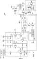
- FIG. 3 depicts a high level schematic of a current sink 300 according to an embodiment.
- Current sink 300 can be implemented, for example, to provide gate pull-down circuit 114 and control signal CSB.
- Current sink 300 includes two NMOS transistors MN0 and MN2 that are coupled to pull down gate control node 302 when both of NMOS transistors MN0 and MN2 are turned ON.
- Control signal generation circuit 304 is coupled to receive power from a number of voltage inputs, which can include, for example, one or more drains, e.g., DRN1 through DRNX, of power FETs for driving control valves and input from a regulator, such as regulator 216.
- Control signal generation circuit 304 provides two control signals. Control signal CS1 is provided to the gate of NMOS transistor MN0 and control signal CS2 is provided to the gate of NMOS transistor MN2.
- NMOS transistor MN0 acts as a diode when gate control node 302 becomes negative, e.g., due to inductive switching or a battery coupled in reverse, and will block a reverse current through NMOS transistors MN0, MN2.
- the negative voltage must also not be allowed to pull current from control signal generation circuit 304.
- Negative voltage blocking circuit 306 is coupled between control signal generation circuit 304 and the gate of NMOS transistor MN0 to block the effect of a negative voltage on gate control node 302 from reaching control signal generation circuit 304.
- negative voltage blocking circuit 306 When gate control node 302 has a positive voltage, negative voltage blocking circuit 306 will pass the control signal CS1 through to the gate of NMOS transistor MN0, but will block the effect of a negative voltage on gate control node 302. Negative voltage blocking circuit 306 can receive other signals that help to determine when the current should be blocked, e.g., negative voltage blocking circuit 306 can receive the value of gate control node 302, control signal CS2, a supply voltage such as VDD, the ignition signal IGNITION and a reference signal (not specifically shown).
- pull-down current limiting circuit 308 can be coupled to the current through NMOS transistors MN0, MN2 and to the gate of NMOS transistor MN2 to limit the current as desired.
- FIG. 4 shows a specific embodiment of system 400 in which a current sink circuit according to an embodiment is used.
- System 400 includes an NMOS power FET 422 having a drain DRN1 and a source SRC1 that is coupled to control actuator 424.
- the gate of NMOS power FET 422 is coupled to gate control node 402, to which the current sink circuit is coupled.
- the system also includes battery 412 and regulator 414.
- the current sink circuit includes NMOS transistors MN0 and MN2, which are coupled in series between gate control node 402 and the lower rail. In at least one embodiment, the lower rail is ground.
- NMOS transistor MN0 has a respective gate and source coupled together through resistor RGSN so that NMOS transistor MN0 acts as a diode when the voltage on gate control node 402 is negative.
- NMOS transistor MN0 receives control signal CS1 on a respective gate and NMOS transistor MN2 receives control signal CS2 on a respective gate.
- control signal generation circuit 404 provides control signals CS1, CS2
- negative voltage blocking circuit 406 blocks a negative voltage on gate control node 402 from pulling current from control signal generation circuit 404
- pull-down current limiting circuit 408 restricts the amount of current that is pulled out of gate control node 402 when the voltage on gate control node 402 is high.
- control signal generation circuit 404 is coupled to the drains DRN1, DRN2 DRN3 of three separate NMOS power FETs and can receive a voltage from any of these that are powered, i.e., a voltage can be received from any combination of DRN1, DRN2, DRN3. Under some conditions, a voltage can also be received from regulator 414.
- the input from regulator 414 is optional and is necessary only when no voltage is present on the drains but the ignition is OFF. In one embodiment, regulator 414 provides a voltage of 3.6 volts. Drains DRN1, DRN2, DRN3 and regulator 414 are tied to battery 412 and accordingly can experience the voltage swings that are inherent in many automotive circuits.
- NMOS transistor M3 has a drain that is coupled to common voltage node 410 and a source that is coupled to the lower rail through Zener diode DN4. The source of NMOS transistor M3 is also coupled to provide control signal CS2, which is used to control the gate of NMOS transistor MN2. Battery 412 is coupled to regulator 414 and regulator 414 is coupled to the source of NMOS transistor M3 through Zener diode DN6.
- NMOS transistor M5 also has a drain coupled to the source of NMOS transistor M3 and a source coupled to the lower rail through current sink 416. When the ignition is turned ON, current sink 416 can couple control signal CS2 to ground.
- NMOS transistors M1 and M2 are coupled in series between common voltage node 410 and the negative voltage blocking circuit 406 and provide control signal CS1.
- the gates of NMOS transistors M1, M2 and M3 are controlled in common by gate node 417, which is coupled to the common voltage node through resistor RLIMIT and is also coupled to the lower rail through Zener diode DN5. It is desirable to provide NMOS transistors M1 and M2 in this back-to-back configuration as a protection against a high voltage, e.g. 40 volts, being received on any of drains DRN1, DRN2, DRN3.
- Zener diode DN5 ensures that the voltage on gate node 417 does not exceed 5.5 volts, but this can cause a source/gate voltage of around 35 volts if a single transistor is used in this position.
- NMOS transistors M1 and M2 in the back-to-back configuration shown, the two transistors protect each other.
- NMOS transistor M4 is also coupled between gate node 417 and the lower rail and is controlled by the ignition signal.
- control signals CS1 and CS2 will be provided at the outputs of control signal generation circuit 404 and have values of about 1.7 volts. If regulator 414 is also providing a voltage, control signal CS2 can carry a voltage of around 3 volts. If only one or two of the drain DRN1, DRN2, DRN3 are active, Zener diodes DN1, DN2, DN3 prevent a backflow of charge through the input nodes. Zener diode DN6 prevents a similar backflow of charge to the regulator 414.
- the maximum gate/source voltage that can be tolerated by the technology is 5 volts; Zener diode DN5 allows voltages above the limit to flow to ground. Zener diode DN4 provides similar protection on control signal CS2.
- NMOS transistor M4 When the ignition is turned ON, NMOS transistor M4 will draw down the gate node 417 of NMOS transistors M1, M2, M3, turning OFF both of control signals CS1, CS2. NMOS transistor M5 will likewise couple control signal CS2 to ground when the ignition is ON.
- Negative voltage blocking circuit 406 includes two P-type metal oxide silicon (PMOS) transistors MP1, MP2, which are coupled in series between control signal generation circuit 404 and the gate of NMOS transistor MN0 and have their gates coupled together.
- PMOS metal oxide silicon
- Zener diode D1 and resistor RGS1 are coupled in parallel between the common node between PMOS transistors MP1, MP2 and their common gate node.
- NMOS transistor MN1 and PMOS transistor MP3 are coupled in series between the common gate node of PMOS transistors MP1, MP2 and the lower rail.
- NMOS transistor MN1 is controlled by control signal CS2 and the gate of PMOS transistor MP3 is controlled by comparator/logic circuit 418 that compares the value on the gate control node 402 against zero and turns PMOS transistor MP3 OFF when gate control node 402 is less than zero.
- Comparator/logic circuit 418 receives power from a voltage source VDD, which in one embodiment is 5 volts.
- NMOS transistor MN1 is ON when power is supplied by the drains DRN1, DRN2, DRN3 and can be supplemented when the regulator is also providing a voltage to the circuit.
- PMOS transistor MP3 is ON when the voltage on gate control node 402 is greater than or equal to zero, pulling the gates of PMOS transistors MP1, MP2 low to hold these PMOS transistors ON to allow control signal CS1 to pass through without attenuation.
- comparator/logic circuit 418 provides a high value on the gate of PMOS transistor MP3, turning OFF this transistor and interrupting the pull-down of the gate nodes of PMOS transistors MP1, MP2 to turn OFF these two transistors. Turning OFF PMOS transistors MP1, MP2 prevents a negative voltage on gate control node 402 from pulling a current from control signal generator circuit 404.
- pull-down current limiting circuit 408 includes two NMOS transistors MN3 and MN5 and sense resistor RSENSE.
- the drain of NMOS transistor MN3 is coupled to node 430, which lies between the two pull-down NMOS transistors MN0, MN2 and the source of NMOS transistor MN3 is coupled to the lower rail through sense resistor RSENSE.
- NMOS transistor MN5 is coupled between control signal CS2 and the lower rail and the gate of NMOS transistor MN5 is coupled to sense node 420, which lies between the source of NMOS transistor MN3 and sense resistor RSENSE.
- pull-down current limiting circuit 408 limits the current through pull-down NMOS transistors MN0, MN2 to 400 mA.
- Table 1 Summary of some of these voltage situations to provide an overview of the operation of the described circuit.
- Control signal CS2 because of the additional voltage from regulator 414, has a value of about 3 V, which turns ON the gate of NMOS transistor MN2, so that a current of 10 mA flows through NMOS transistors NM0, NM2, and also turns ON NMOS transistor MN1 to ensure that the gates of PMOS transistors MP1, MP2 are pulled down.
- control signal CS1 remains at about 1.8 V and control signal CS1 is about 1.7 V, which is still sufficient to turn ON NMOS transistor MN2 and MN1 to pull down the gates of PMOS transistors MP1, MP2.
- the voltage on node 426 is equal to the voltage on gate node 417 minus the threshold voltage of NMOS transistor M1, and this voltage is passed through PMOS transistors MP1, MP2 to node 428. If the gate control node 402 goes up to 40 V, whether the voltage on common voltage node 410 is 4 V or 40 V, the current through NMOS transistor MN2 is limited by the pull-down current limiting circuit 408 and will not exceed 400 mA in one embodiment.
- node 426 is limited to the voltage on gate node 417 minus the threshold voltage of NMOS transistor M1 and when GCN 402 has a higher voltage than the common voltage node 410, node 426 tracks node 428 as long as GCN 402 has a positive voltage.
- node 428 will track GCN 402.
- the negative voltage on GCN 402 causes comparator/logic circuit 418 to turn OFF PMOS transistor MP3, which in turn turns OFF PMOS transistors MP1, MP2, so node 426 is not disturbed by the negative voltage.
- the ignition will be OFF and both GCN 402 and the drains DRN1, DRN2, DRN3 are negative.
- PMOS transistor MP3 and NMOS transistor MN1 are OFF, which causes PMOS transistors MP1, MP2 to turn OFF.
- Node 428 tracks GCN 402 and prevents current flow from the substrate to GCN 402.
- comparator/logic circuit 418 turns PMOS transistor MP3 OFF to turn OFF PMOS transistors MP1, MP2.
- Node 428 again tracks GCN 402 and prevents any current flow from the substrate to GCN 402.
- FIG. 5 depicts an example schematic of a portion of an automotive system 500 in which a chip 502 containing the described current sink operates according to an embodiment.
- automotive system 500 includes a battery 514 supplying power to chip 502 and actuators 512 that are controlled by chip 502.
- Chip 502 is a system-on-chip that will be used to electronically control multiple systems, e.g., windows, door locks, braking systems, etc., at least some of which are considered safety critical.
- Chip 502 contains a power supply module 504 that is coupled to the battery through an external contact, which can be a lead that is part of a leadframe, a bump in a bump array or any other type of external connector.
- transceivers 506 are coupled to receive power from power supply module and to provide communications across various bus systems throughout the automotive environment.
- transceiver 506-1 is for FlexRay, which is a bus system for security-critical applications.
- Transceiver 506-2 is for the controller area network (CAN), which enables the networking of a large number of engine controller units (ECUs) that control actuators on an internal combustion engine to ensure optimal engine performance.
- Transceiver 506-3 is for Local INterconnect (LIN), which enables the integration of sensors and actuators in vehicle networks. Other networks can also be used within the automotive environment, and their associated transceivers can also be included in chip 502 as necessary or desired.
- LIN Local INterconnect
- Chip 502 also contains a number of valve drivers 510 and current sink circuits 508. As shown, the gates of a number of power NMOS FETs 520 can each be coupled to a respective current sink circuit 508 through a connector 516 for the gate control node so that the power NMOS FET is held OFF when the ignition is OFF.
- the source of each power NMOS FET 520 is coupled to one terminal of an actuator 512, and a second terminal of the actuator 512 is coupled to a respective valve driver 510 through a respective connector 518.
- actuator 512 Although a single actuator 512 is shown as connected between a respective NMOS FET 520 and a respective valve driver 510, a group of actuators 512 that operate in unison can be coupled between a valve driver 510 and power NMOS FET 520.
- the current sink circuit is used to pull down the gate control node of an NMOS power FET to ensure that the power FET does not turn ON inadvertently.
- the current sink circuit operates to provide the desired pull-down current whenever a voltage of at least 0.5 volts is present on the gate control node.
- the current sink circuit can operate properly with voltages that range from -25 volts to 40 volts in line with the harsh automotive environment in which they will operate.
Landscapes
- Engineering & Computer Science (AREA)
- Physics & Mathematics (AREA)
- Microelectronics & Electronic Packaging (AREA)
- Transportation (AREA)
- Mechanical Engineering (AREA)
- Nonlinear Science (AREA)
- Electromagnetism (AREA)
- General Physics & Mathematics (AREA)
- Radar, Positioning & Navigation (AREA)
- Automation & Control Theory (AREA)
- Fluid Mechanics (AREA)
- Electronic Switches (AREA)
Description
- This relates generally to current sinks, and more particularly to a current sink with negative voltage tolerance.
- In some safety critical situations, such as automotive braking applications, an actuator must not be turned ON inadvertently. This means that the actuator must turn ON only when software initiates a turn ON condition and must remain OFF in all other conditions. When the actuator is controlled by an N-type metal oxide silicon (NMOS) power field effect transistor (FET) serving as the relay driver, the OFF condition should be ensured by a strong gate pull down current. To operate effectively and economically, the pull down current should be active under any phase of operation, have a low overall quiescent current, and be able to operate in a harsh automotive environment that includes fast battery transients and inductive switching that can result in voltage levels of 40V and -25V.
WO 2015/056042 discloses an IGBT driver module and method therefor.EP 2 073 386WO 2016/170724 discloses a solid state relay. - Described embodiments include a circuit that provides a strong gate pull down current using multiple voltage inputs while protecting the circuit from both high and low transient voltages. A voltage to drive the pull down circuit can be drawn from the drains of one or more control NMOS power FETs, other sources tied to the battery or to additional voltages available when the ignition is ON. Elements of the circuit are protected from high voltages and negative voltages.
- In one aspect, a current sink circuit is coupled to pull down a gate control node for an N-type metal oxide (NMOS) power field effect transistor (FET) that controls an actuator. The current sink circuit includes a first NMOS transistor coupled in series with a second NMOS transistor between the gate control node and a lower rail. The first NMOS transistor has a respective gate and source coupled together through a first resistor. A control signal generation circuit is coupled to receive at least one voltage input and an ignition signal and is further coupled to provide a first control signal and a second control signal. The second control signal is coupled to the gate of the second NMOS transistor. A negative voltage blocking circuit is coupled to pass the first control signal from the control signal generation circuit to the gate of the first NMOS transistor and to block a negative voltage on the gate control node from reaching the control signal generation circuit.
- In another aspect, a system-on-chip (SOC) includes a power supply module coupled to a connector for coupling to a battery. Transceivers are coupled to the power supply modules. Valve drivers are coupled to respective connectors for connection to a respective actuator. Current sink circuits are coupled to pull down a gate control node for a respective N-type metal oxide (NMOS) power field effect transistor (FET) that switches a respective valve driver of the valve drivers and a respective actuator coupled thereto. One of the current sink circuits includes: a first NMOS transistor coupled in series with a second NMOS transistor between the gate control node and a lower rail, the first NMOS transistor having a respective gate and source coupled together through a first resistor; a control signal generation circuit coupled to receive at least one voltage input and an ignition signal and further coupled to provide a first control signal and a second control signal, the second control signal being coupled to the gate of the second NMOS transistor; and a negative voltage blocking circuit coupled to pass the first control signal from the control signal generation circuit to the gate of the first NMOS transistor and to block a negative voltage on the gate control node from reaching the control signal generation circuit.
-
-
FIG. 1 depicts an example of a braking actuator in which a current sink according to an embodiment can be used. -
FIG. 2 depicts further details of an example braking actuator to describe various issues to overcome. -
FIG. 3 depicts high level schematic of a current sink according to an embodiment. -
FIG. 4 depicts an implementation of a current sink circuit according to an embodiment. -
FIG. 5 depicts an example schematic of a portion of an automotive system in which a chip containing the described current sink operates according to an embodiment. -
FIG. 6 depicts an implementation of a conventional current sink. -
FIG. 7 depicts a further implementation of a conventional current sink. - In the drawings, like references indicate similar elements. In this description, the term "couple" or "couples" means either an indirect or direct electrical connection unless qualified as in "communicably coupled" which may include wireless connections. Thus, if a first device couples to a second device, that connection may be through a direct electrical connection, or through an indirect electrical connection via other devices and connections.
-
FIG. 1 depicts an example of a schematic for anactuator control system 100 for an automotive application in which a current sink according to this description can be used.Actuator control system 100 includes an NMOS power FET 106 that controls a current betweendrain 108 andsource 110.Source 110 is coupled tovalve driver 112 that controls specific valves in the vehicle to effect, e.g., braking. A control signal CSA is provided todriver 102, which in turn is coupled to provide a control signal on gate control node (GCN) 104 to turn NMOS power FET 106 ON and OFF. As described hereinabove, NMOS power FET 106 must not turn ON unless driven to turn ON bydriver 102. To avoid inadvertently turning ONNMOS power FET 106, a gate pull-down circuit 114 is selectively coupled betweengate control node 104 and the lower rail by a switch S1 that is controlled by control signal CSB. In one embodiment, control signals CSA and CSB have opposite logic values. Accordingly, when control signal CSA is high, NMOS power FET 106 is turned ON, control signal CSB is low and opens switch S1. When control signal CSA is low, control signal CSB is high and closes switch S1, pulling downgate control node 104. Gate pull-downcircuit 114 needs to be active under any phase of operation, yet maintain a low quiescent current from the battery. Gate pull-downcircuit 114 must be able to handle fast battery transients and inductive switching and the resulting voltage levels of 40V to -25V. -
FIG. 2 provides a schematic of an exampleactuator control system 200 that provides somewhat greater detail to describe some of the needs of the specific application.Actuator control system 200 includes NMOS power FET 206, which is coupled to gate control node GCN 204, drain 208C andsource 210. NMOS power FET 206, when turned ON, will supply power tovalve driver 212. In this embodiment, NMOS power FET 206 is one of three switches that are each tied to a separate valve driver, although the other two NMOS power FETs are not shown and are represented only by theirrespective drains drains respective drivers driver 202C. - Within
driver 202C, pulse width modulation (PWM)current source 220 sources current togate control node 204 when switch S2 is closed and PWM current sink 222 sinks current fromgate control node 204 when switch S3 is closed. PWMcurrent source 220 and PWM current sink 222 are active to control NMOS power FET 206 when the ignition for the vehicle is turned ON. When the ignition is OFF,switch S 1 is closed and gate current sink 224 sinks current fromGCN 204. - When a user with an electronic key is near the vehicle, wake-
up detection circuit 214 enables several functions in the vehicle; these functions in turn provide an ultra-low current output The ultra-low current is provided to aregulator 216, which also acts as a bias generator. The wake-up detection circuit 214 andregulator 216 are selectively coupled tocharge pump 218 through switch S4.Charge pump 218 is further coupled to driver 202 to provide a voltage to PWMcurrent source 220. - It is desirable to have gate current sink 224 be activated from
GCN 204 when any of the following conditions is true: (a) pulse width modulation is OFF; (b) the ignition is OFF; (c) battery power is supplied; or (d) any combinations of drains 208 carries a minimum of 3 volts. In one embodiment, the following conditions are desirable: - the pull down current through
NMOS power FET 206 is greater than 7 mA when the voltage on the combination of drains 208 is between 3 and 40 volts andGCN 204 has a low value, e.g., 0.5 volts; - the pull-down current is less than 400 mA when the voltage on the combination of drains 208 is between 3 and 40 volts and
GCN 204 has a high value, e.g., 20 volts; - the sum of currents through drains 208 is less than 5 µA at 14 volts input;
- negative voltages on
GCN 204 are blocked up to -25 volts; and - the pull down current is OFF when the ignition is ON.
-
FIG. 6 depicts an example of a conventionalcurrent sink 600. Incurrent sink 600, regulator andbias generator 604 is coupled tobattery 602 and to current source IBIAS 606, which sources a current to the drain ofNMOS transistor 608.NMOS transistor 608 has a source coupled to the lower rail, a gate and drain coupled together, and forms a current mirror withNMOS transistor 610, which is coupled betweengate control node 614 and the lower rail.NMOS transistor 610 sinks current fromgate control node 614, withdiode 612 ensuring that current does not flow out ofcurrent sink 600, even ifGCN 614 has a negative voltage. -
Current sink 600 has several issues. First, the current sink IPULLDWN does not sink any current whenGCN 614 is equal to 0.5 volts becausediode 612 usually requires at least 0.7 volts to pass a current. Also, the bias current IBIAS is zero if battery power is not available, even when a voltage exists on one or more of the drains for the actuators. If regulator andbias generator 604 is supplied by battery power and by the drains, then the sum of currents through drains 208 can exceed the desired 5 µA. -
FIG. 7 depicts an example of a conventionalcurrent sink 700 for use in the actuator ofFIG. 1 . Again, regulator andbias generator 704 is coupled tobattery 702 and tocurrent source IBIAS 706, whileNMOS transistors Circuit 720 has been added betweennode GCN 718 and a newGCN sink node 712, which is coupled to the drain ofNMOS transistor 710.Circuit 720 contains NMOS transistor MN8, which is coupled betweenGCN 718 andGCN sink node 712 and containsdiode 714. The gate of NMOS transistor MN8 is coupled to the drain of NPN transistor Q1, and the source of NPN transistor Q1 is coupled through diode D3 to anode 716 that lies betweenGCN 718 anddiode 714. The drain of NPN transistor Q1 is coupled tonode 716 through resistor R2. Diode D2 is coupled betweennode 716 and the gate of NMOS transistor MN8 and also to voltage VCPE through resistor R1. The gate of NPN transistor Q1 is coupled to the lower rail throughresistor R3. Circuit 720 is an external circuit; when this solution is integrated into a chip, the diodes cannot be added to NMOS transistor MN8, since these diodes are created from on chip NPN transistors prohibiting -25V operation. Also, it is not possible to ensure that the gate/source voltage of NMOS transistor MN8 is limited to a maximum value of 5.5 volts, which is the maximum the technology allows. Accordingly, it is not possible to incorporate this circuit into a system-on chip or similar type chip. -
FIG. 3 depicts a high level schematic of acurrent sink 300 according to an embodiment.Current sink 300 can be implemented, for example, to provide gate pull-down circuit 114 and control signal CSB.Current sink 300 includes two NMOS transistors MN0 and MN2 that are coupled to pull downgate control node 302 when both of NMOS transistors MN0 and MN2 are turned ON. Controlsignal generation circuit 304 is coupled to receive power from a number of voltage inputs, which can include, for example, one or more drains, e.g., DRN1 through DRNX, of power FETs for driving control valves and input from a regulator, such asregulator 216. Except for the drain of the NMOS power FET that is controlled bygate control node 302, all of these voltage inputs are optional, although their inclusion may be desirable in at least some applications. An ignition signal, IGNITION, is also received to enable the detection of when the ignition is ON. Controlsignal generation circuit 304 provides two control signals. Control signal CS1 is provided to the gate of NMOS transistor MN0 and control signal CS2 is provided to the gate of NMOS transistor MN2. - Because the gate and source of NMOS transistor MN0 are coupled together, NMOS transistor MN0 acts as a diode when
gate control node 302 becomes negative, e.g., due to inductive switching or a battery coupled in reverse, and will block a reverse current through NMOS transistors MN0, MN2. However, the negative voltage must also not be allowed to pull current from controlsignal generation circuit 304. Negativevoltage blocking circuit 306 is coupled between controlsignal generation circuit 304 and the gate of NMOS transistor MN0 to block the effect of a negative voltage ongate control node 302 from reaching controlsignal generation circuit 304. Whengate control node 302 has a positive voltage, negativevoltage blocking circuit 306 will pass the control signal CS1 through to the gate of NMOS transistor MN0, but will block the effect of a negative voltage ongate control node 302. Negativevoltage blocking circuit 306 can receive other signals that help to determine when the current should be blocked, e.g., negativevoltage blocking circuit 306 can receive the value ofgate control node 302, control signal CS2, a supply voltage such as VDD, the ignition signal IGNITION and a reference signal (not specifically shown). - Also, in many instances, it is desirable to limit the amount of pull-down current that is drawn off of
gate control node 302 when the voltage ongate control node 302 is high, e.g., 14 volts. When limiting the pull-down current is desired, pull-down current limitingcircuit 308 can be coupled to the current through NMOS transistors MN0, MN2 and to the gate of NMOS transistor MN2 to limit the current as desired. -
FIG. 4 shows a specific embodiment ofsystem 400 in which a current sink circuit according to an embodiment is used.System 400 includes anNMOS power FET 422 having a drain DRN1 and a source SRC1 that is coupled to controlactuator 424. The gate ofNMOS power FET 422 is coupled togate control node 402, to which the current sink circuit is coupled. The system also includesbattery 412 andregulator 414. The current sink circuit includes NMOS transistors MN0 and MN2, which are coupled in series betweengate control node 402 and the lower rail. In at least one embodiment, the lower rail is ground. Similar tocurrent sink 300, NMOS transistor MN0 has a respective gate and source coupled together through resistor RGSN so that NMOS transistor MN0 acts as a diode when the voltage ongate control node 402 is negative. NMOS transistor MN0 receives control signal CS1 on a respective gate and NMOS transistor MN2 receives control signal CS2 on a respective gate. Three additional circuits are part of the current sink circuit: controlsignal generation circuit 404 provides control signals CS1, CS2, negativevoltage blocking circuit 406 blocks a negative voltage ongate control node 402 from pulling current from controlsignal generation circuit 404, and pull-down current limitingcircuit 408 restricts the amount of current that is pulled out ofgate control node 402 when the voltage ongate control node 402 is high. - In this example embodiment, control
signal generation circuit 404 is coupled to the drains DRN1, DRN2 DRN3 of three separate NMOS power FETs and can receive a voltage from any of these that are powered, i.e., a voltage can be received from any combination of DRN1, DRN2, DRN3. Under some conditions, a voltage can also be received fromregulator 414. The input fromregulator 414 is optional and is necessary only when no voltage is present on the drains but the ignition is OFF. In one embodiment,regulator 414 provides a voltage of 3.6 volts. Drains DRN1, DRN2, DRN3 andregulator 414 are tied tobattery 412 and accordingly can experience the voltage swings that are inherent in many automotive circuits. Each of drains DRN1, DRN2, DRN3 is coupled to provide input to controlsignal generation circuit 404 through a respective resistor RN1, RN2, RN3 and a respective Zener diode DN1, DN2, DN3. The voltages received from drains DRN1, DRN2 DRN3 are coupled together at acommon voltage node 410. - NMOS transistor M3 has a drain that is coupled to
common voltage node 410 and a source that is coupled to the lower rail through Zener diode DN4. The source of NMOS transistor M3 is also coupled to provide control signal CS2, which is used to control the gate of NMOS transistor MN2.Battery 412 is coupled toregulator 414 andregulator 414 is coupled to the source of NMOS transistor M3 through Zener diode DN6. NMOS transistor M5 also has a drain coupled to the source of NMOS transistor M3 and a source coupled to the lower rail throughcurrent sink 416. When the ignition is turned ON,current sink 416 can couple control signal CS2 to ground. - NMOS transistors M1 and M2 are coupled in series between
common voltage node 410 and the negativevoltage blocking circuit 406 and provide control signal CS1. The gates of NMOS transistors M1, M2 and M3 are controlled in common bygate node 417, which is coupled to the common voltage node through resistor RLIMIT and is also coupled to the lower rail through Zener diode DN5. It is desirable to provide NMOS transistors M1 and M2 in this back-to-back configuration as a protection against a high voltage, e.g. 40 volts, being received on any of drains DRN1, DRN2, DRN3. In this situation, Zener diode DN5 ensures that the voltage ongate node 417 does not exceed 5.5 volts, but this can cause a source/gate voltage of around 35 volts if a single transistor is used in this position. By providing NMOS transistors M1 and M2 in the back-to-back configuration shown, the two transistors protect each other. NMOS transistor M4 is also coupled betweengate node 417 and the lower rail and is controlled by the ignition signal. - In one embodiment, whenever a voltage on any of drains DRN1, DRN2, DRN3 is at least three volts, control signals CS1 and CS2 will be provided at the outputs of control
signal generation circuit 404 and have values of about 1.7 volts. Ifregulator 414 is also providing a voltage, control signal CS2 can carry a voltage of around 3 volts. If only one or two of the drain DRN1, DRN2, DRN3 are active, Zener diodes DN1, DN2, DN3 prevent a backflow of charge through the input nodes. Zener diode DN6 prevents a similar backflow of charge to theregulator 414. - In one embodiment, the maximum gate/source voltage that can be tolerated by the technology is 5 volts; Zener diode DN5 allows voltages above the limit to flow to ground. Zener diode DN4 provides similar protection on control signal CS2. When the ignition is turned ON, NMOS transistor M4 will draw down the
gate node 417 of NMOS transistors M1, M2, M3, turning OFF both of control signals CS1, CS2. NMOS transistor M5 will likewise couple control signal CS2 to ground when the ignition is ON. - Negative
voltage blocking circuit 406 includes two P-type metal oxide silicon (PMOS) transistors MP1, MP2, which are coupled in series between controlsignal generation circuit 404 and the gate of NMOS transistor MN0 and have their gates coupled together. Zener diode D1 and resistor RGS1 are coupled in parallel between the common node between PMOS transistors MP1, MP2 and their common gate node. NMOS transistor MN1 and PMOS transistor MP3 are coupled in series between the common gate node of PMOS transistors MP1, MP2 and the lower rail. The gate of NMOS transistor MN1 is controlled by control signal CS2 and the gate of PMOS transistor MP3 is controlled by comparator/logic circuit 418 that compares the value on thegate control node 402 against zero and turns PMOS transistor MP3 OFF whengate control node 402 is less than zero. Comparator/logic circuit 418 receives power from a voltage source VDD, which in one embodiment is 5 volts. - During operation of the pull-down circuit, NMOS transistor MN1 is ON when power is supplied by the drains DRN1, DRN2, DRN3 and can be supplemented when the regulator is also providing a voltage to the circuit. PMOS transistor MP3 is ON when the voltage on
gate control node 402 is greater than or equal to zero, pulling the gates of PMOS transistors MP1, MP2 low to hold these PMOS transistors ON to allow control signal CS1 to pass through without attenuation. However, when the value ofgate control node 402 drops below zero, comparator/logic circuit 418 provides a high value on the gate of PMOS transistor MP3, turning OFF this transistor and interrupting the pull-down of the gate nodes of PMOS transistors MP1, MP2 to turn OFF these two transistors. Turning OFF PMOS transistors MP1, MP2 prevents a negative voltage ongate control node 402 from pulling a current from controlsignal generator circuit 404. - Finally, pull-down current limiting
circuit 408 includes two NMOS transistors MN3 and MN5 and sense resistor RSENSE. The drain of NMOS transistor MN3 is coupled tonode 430, which lies between the two pull-down NMOS transistors MN0, MN2 and the source of NMOS transistor MN3 is coupled to the lower rail through sense resistor RSENSE. NMOS transistor MN5 is coupled between control signal CS2 and the lower rail and the gate of NMOS transistor MN5 is coupled tosense node 420, which lies between the source of NMOS transistor MN3 and sense resistor RSENSE. As the current flowing through pull-down NMOS transistors MN0, MN2 increases, the voltage onsense node 420 also increases and turns ON NMOS transistor MN5. This action draws down the voltage carried on control signal CS2 and serves to limit the current passing through NMOS transistors MN0 and MN2 as a result. In one embodiment, pull-down current limitingcircuit 408 limits the current through pull-down NMOS transistors MN0, MN2 to 400 mA. - Given the variability of the voltages appearing on the various drains and on
gate control node 402, many conditions have to be protected against in one way or another. Table 1 below summarizes some of these voltage situations to provide an overview of the operation of the described circuit.Table 1 Condition Mode of Operation Signals MP1/ MP2 MNO mode Gate control node is positive (≥0.5 V) Standby Ignition OFF CS1 = 1.8 V, ON Switch (at least 10mA pulldown on Gate control node) CS2 = 3 V MP3 = 0 V Gate control node is positive (≥0.5 V) DRNx>3 V Only DRNx voltage available Ignition OFF CS1=1.8 V ON Switch (at least 10mA pulldown on Gate control node) CS2 = 1.7 V MP3 = 0 V Gate control node is negative (-25 V) Ignition ON (VDD=5V) CS2 = 0 V OFF Diode MP3 (GATE) = 3 V - As described hereinabove, by the time the
gate control node 402 reaches 0.5 volts, the current sink should be turned on to pull the gate control node towards ground whenever the ignition is OFF. This situation is shown in both the first and second entries of Table 1, wheregate control node 402 is greater than or equal to 0.5 volts and the ignition is OFF. In both of these entries, the drains orcommon voltage node 410 is about 3 volts, while the difference between these two entries is whether or not any voltage is available fromregulator 414. In the first entry, a voltage from the regulator of about 3.6 volts is available. Control signal CS1 has a voltage of about 1.8 V, which is sufficient to turn ON NMOS transistor MN0. Control signal CS2, because of the additional voltage fromregulator 414, has a value of about 3 V, which turns ON the gate of NMOS transistor MN2, so that a current of 10 mA flows through NMOS transistors NM0, NM2, and also turns ON NMOS transistor MN1 to ensure that the gates of PMOS transistors MP1, MP2 are pulled down. - In the second entry, voltage from
regulator 414 is not available, so only the drains determine the value of control signal CS2. In this situation, control signal CS1 remains at about 1.8 V and control signal CS1 is about 1.7 V, which is still sufficient to turn ON NMOS transistor MN2 and MN1 to pull down the gates of PMOS transistors MP1, MP2. - In both of these situations, the voltage on node 426 is equal to the voltage on
gate node 417 minus the threshold voltage of NMOS transistor M1, and this voltage is passed through PMOS transistors MP1, MP2 tonode 428. If thegate control node 402 goes up to 40 V, whether the voltage oncommon voltage node 410 is 4 V or 40 V, the current through NMOS transistor MN2 is limited by the pull-down current limitingcircuit 408 and will not exceed 400 mA in one embodiment. More generally, when the voltage on thecommon voltage node 410 is greater than the voltage onGCN 402, node 426 is limited to the voltage ongate node 417 minus the threshold voltage of NMOS transistor M1 and whenGCN 402 has a higher voltage than thecommon voltage node 410, node 426tracks node 428 as long asGCN 402 has a positive voltage. - If
gate control node 402 is negative, as shown in the third entry in Table 1,node 428 will trackGCN 402. However, the negative voltage onGCN 402 causes comparator/logic circuit 418 to turn OFF PMOS transistor MP3, which in turn turns OFF PMOS transistors MP1, MP2, so node 426 is not disturbed by the negative voltage. In the special condition where the battery is accidently connected in reverse, the ignition will be OFF and bothGCN 402 and the drains DRN1, DRN2, DRN3 are negative. PMOS transistor MP3 and NMOS transistor MN1 are OFF, which causes PMOS transistors MP1, MP2 to turn OFF.Node 428tracks GCN 402 and prevents current flow from the substrate toGCN 402. If the ignition is ON and GCN is negative while the drain is positive, comparator/logic circuit 418 turns PMOS transistor MP3 OFF to turn OFF PMOS transistors MP1, MP2.Node 428 again tracksGCN 402 and prevents any current flow from the substrate toGCN 402. -
FIG. 5 depicts an example schematic of a portion of anautomotive system 500 in which achip 502 containing the described current sink operates according to an embodiment. In this embodiment,automotive system 500 includes abattery 514 supplying power to chip 502 and actuators 512 that are controlled bychip 502.Chip 502 is a system-on-chip that will be used to electronically control multiple systems, e.g., windows, door locks, braking systems, etc., at least some of which are considered safety critical.Chip 502 contains apower supply module 504 that is coupled to the battery through an external contact, which can be a lead that is part of a leadframe, a bump in a bump array or any other type of external connector. - A number of transceivers 506 are coupled to receive power from power supply module and to provide communications across various bus systems throughout the automotive environment. In the embodiment shown, transceiver 506-1 is for FlexRay, which is a bus system for security-critical applications. Transceiver 506-2 is for the controller area network (CAN), which enables the networking of a large number of engine controller units (ECUs) that control actuators on an internal combustion engine to ensure optimal engine performance. Transceiver 506-3 is for Local INterconnect (LIN), which enables the integration of sensors and actuators in vehicle networks. Other networks can also be used within the automotive environment, and their associated transceivers can also be included in
chip 502 as necessary or desired. -
Chip 502 also contains a number of valve drivers 510 and current sink circuits 508. As shown, the gates of a number of power NMOS FETs 520 can each be coupled to a respective current sink circuit 508 through a connector 516 for the gate control node so that the power NMOS FET is held OFF when the ignition is OFF. The source of each power NMOS FET 520 is coupled to one terminal of an actuator 512, and a second terminal of the actuator 512 is coupled to a respective valve driver 510 through a respective connector 518. Although a single actuator 512 is shown as connected between a respective NMOS FET 520 and a respective valve driver 510, a group of actuators 512 that operate in unison can be coupled between a valve driver 510 and power NMOS FET 520. - In the described current sink circuit and chip, the current sink circuit is used to pull down the gate control node of an NMOS power FET to ensure that the power FET does not turn ON inadvertently. The current sink circuit operates to provide the desired pull-down current whenever a voltage of at least 0.5 volts is present on the gate control node. The current sink circuit can operate properly with voltages that range from -25 volts to 40 volts in line with the harsh automotive environment in which they will operate.
- Modifications are possible in the described embodiments, and other embodiments are possible, within the scope of the claims.
Claims (15)
- A current sink circuit coupled to pull down a gate control node (402) for an N-type metal oxide NMOS power field effect transistor FET (422) that controls an actuator (424), the current sink circuit comprising:a first NMOS transistor (MNO) coupled in series with a second NMOS transistor (MN2) between the gate control node (402) and a lower rail, the first NMOS transistor (MNO) having a respective gate and source coupled together through a first resistor (RGSN);a control signal generation circuit (404) coupled to receive at least one voltage input and an ignition signal and further coupled to provide a first control signal (CS1) and a second control signal (CS2), the control signal generation circuit coupled to provide the second control signal (CS2) to the gate of the second NMOS transistor (MN2); anda negative voltage blocking circuit (406) coupled to pass the first control signal (CS1) from the control signal generation circuit (404) to the gate of the first NMOS transistor (MNO) and to block a negative voltage on the gate control node (402) from reaching the control signal generation circuit (404).
- The current sink circuit as recited in claim 1 wherein the control signal generation circuit (404) comprises:a common voltage node that is coupled to the at least one voltage input through at least one respective second resistor and at least one respective first Zener diode, the second resistor and the first Zener diode coupled in series;a third NMOS transistor having a drain coupled to the common voltage node and a source coupled to the lower rail through a second Zener diode, a node between the source of the third NMOS transistor and the second Zener diode providing the second control signal (CS2);a fourth NMOS transistor and a fifth NMOS transistor coupled in series between the common voltage node and the negative voltage blocking circuit (406) and providing the first control signal (CS1);a gate node coupled to the gates of the third, fourth and fifth NMOS transistors, the gate node being further coupled to the common voltage node through a third resistor and to the lower rail through a third Zener diode; anda sixth NMOS transistor coupled between the gate node and the lower rail, the gate of the sixth NMOS transistor coupled to receive the ignition signal.
- The current sink circuit as recited in claim 1 further comprising a seventh NMOS transistor coupled between the second control signal (CS2) and a further current sink.
- The current sink circuit as recited in claim 1 wherein the negative voltage blocking circuit (406) comprises:a first P-type metal oxide silicon PMOS transistor coupled in series with a second PMOS transistor between the control signal generation circuit (404) and the gate of the first NMOS transistor (MNO), the gates of the first and second PMOS transistors being coupled together;a fifth Zener diode and a fourth resistor coupled in parallel between the gates of the first and second PMOS transistors and a node lying between the first and second PMOS transistors;an eighth NMOS transistor having a drain coupled to the gates of the first and second PMOS transistors and a gate coupled to receive the second control signal (CS2); anda third PMOS transistor having a source coupled to the source of the eighth NMOS transistor, a drain coupled to the lower rail and a gate that is controlled by logic circuit that is coupled to turn OFF the third PMOS transistor when the voltage on the gate control node (402) is less than a reference voltage.
- The current sink circuit as recited in claim 1 further comprising a pull-down current limiting circuit coupled to receive the second control signal (CS2) and a voltage taken between the first and second NMOS transistors (MNO, MN2) and to limit the amount of current pulled from the gate control node (402).
- The current sink circuit as recited in claim 5 wherein the pull-down current limiting circuit comprises:a ninth NMOS transistor having a drain coupled between the first and second NMOS transistors (MNO, MN2), a gate coupled to receive the second control signal (CS2) and a source coupled to the lower rail through a sense resistor; anda tenth NMOS transistor having a drain coupled to the second control signal (CS2), a source coupled to the lower rail and a gate coupled between the ninth NMOS transistor and the sense resistor.
- A system-on-chip SOC comprising:a power supply module coupled to a connector for coupling to a battery;a plurality of transceivers coupled to the power supply modules;a plurality of valve drivers coupled to respective connectors for connection to a respective actuator;
a plurality of current sink circuits according to claim 1 coupled to pull down a gate control node for a respective N-type metal oxide NMOS power field effect transistor FET (422) that is configured to switch a respective valve driver of the plurality of valve drivers and a respective actuator coupled thereto. - The SOC as recited in claim 7 wherein the control signal generation circuit (404) comprises:a common voltage node that is coupled to the at least one voltage input through at least one respective second resistor and at least one respective first Zener diode;a third NMOS transistor having a drain coupled to the common voltage node and a source coupled to a lower rail through a second Zener diode, a node between the source of the third NMOS transistor and the second Zener diode providing the second control signal (CS2);a fourth NMOS transistor and a fifth NMOS transistor coupled in series between the common voltage node and the negative voltage blocking circuit and providing the first control signal (CS1);a gate node coupled to the gates of the third, fourth and fifth NMOS transistors, the gate node being further coupled to the common voltage node through a third resistor and to the lower rail through a third Zener diode; anda sixth NMOS transistor coupled between the gate node and the lower rail, the gate of the sixth NMOS transistor being coupled to an ignition signal.
- The current sink circuit as recited in claim 2 or the SOC as recited in claim 8 wherein the at least one voltage input comprises a drain voltage for the NMOS power FET (422).
- The current sink circuit or SOC as recited in claim 9 wherein the at least one voltage input further comprises respective drain voltages for a plurality of NMOS power FETs (422) that control additional actuators.
- The current sink circuit or SOC as recited in claim 9 wherein the at least one voltage input further comprises a voltage from a regulator, the regulator being coupled to the second control signal (CS2) through a fourth Zener diode.
- The SOC as recited in claim 7 further comprising a seventh NMOS transistor coupled between the second control signal (CS2) and a further current sink.
- The SOC as recited in claim 7 wherein the negative voltage blocking circuit (406) comprises:a first P-type metal oxide silicon PMOS transistor coupled in series with a second PMOS transistor between the control signal generation circuit (404) and the gate of the first NMOS transistor (MNO), the gates of the first and second PMOS transistors being coupled together;a fifth Zener diode and a fourth resistor coupled in parallel between the gates of the first and second PMOS transistors and a node lying between the first and second PMOS transistors;an eighth NMOS transistor having a drain coupled to the gates of the first and second PMOS transistors and a gate coupled to receive the second control signal (CS2); anda third PMOS transistor having a source coupled to the source of the eighth NMOS transistor, a drain coupled to the lower rail and a gate that is controlled by logic circuit that is coupled to turn OFF the third PMOS transistor when the voltage on the gate control node (402) is less than a reference voltage.
- The SOC as recited in claim 7 further comprising a pull-down current limiting circuit coupled to receive the second control signal (CS2) and a voltage taken between the first and second NMOS transistors (MNO, MN2) and to limit the amount of current pulled from the gate control node (402).
- The SOC as recited in claim 14 wherein the pull-down current limiting circuit comprises:a ninth NMOS transistor having a drain coupled between the first and second NMOS transistors (MNO, MN2), a gate coupled to receive the second control signal (CS2) and a source coupled to the lower rail through a sense resistor; anda tenth NMOS transistor having a drain coupled to the second control signal (CS2), a source coupled to the lower rail and a gate coupled between the ninth NMOS transistor and the sense resistor.
Applications Claiming Priority (3)
| Application Number | Priority Date | Filing Date | Title |
|---|---|---|---|
| US201762533864P | 2017-07-18 | 2017-07-18 | |
| US15/832,071 US10520971B2 (en) | 2017-07-18 | 2017-12-05 | Current sink with negative voltage tolerance |
| PCT/US2018/041733 WO2019018189A1 (en) | 2017-07-18 | 2018-07-12 | Current sink with negative voltage tolerance |
Publications (3)
| Publication Number | Publication Date |
|---|---|
| EP3656057A1 EP3656057A1 (en) | 2020-05-27 |
| EP3656057A4 EP3656057A4 (en) | 2020-07-15 |
| EP3656057B1 true EP3656057B1 (en) | 2023-12-13 |
Family
ID=65015323
Family Applications (1)
| Application Number | Title | Priority Date | Filing Date |
|---|---|---|---|
| EP18835338.7A Active EP3656057B1 (en) | 2017-07-18 | 2018-07-12 | Current sink with negative voltage tolerance |
Country Status (3)
| Country | Link |
|---|---|
| US (1) | US10520971B2 (en) |
| EP (1) | EP3656057B1 (en) |
| WO (1) | WO2019018189A1 (en) |
Families Citing this family (3)
| Publication number | Priority date | Publication date | Assignee | Title |
|---|---|---|---|---|
| US10784917B2 (en) | 2018-11-27 | 2020-09-22 | Texas Instruments Incorporated | PSI5 base current sampling in synchronous mode |
| US11581723B2 (en) * | 2020-06-30 | 2023-02-14 | Texas Instruments Incorporated | High voltage tolerant analog-digital output |
| US11502674B2 (en) * | 2020-07-20 | 2022-11-15 | Texas Instruments Incorporated | Optimized low Ron flatness gate driver |
Family Cites Families (10)
| Publication number | Priority date | Publication date | Assignee | Title |
|---|---|---|---|---|
| JPH077404A (en) * | 1992-11-03 | 1995-01-10 | Texas Instr Deutschland Gmbh | Arrangement of transistor drive circuit |
| US5789951A (en) | 1997-01-31 | 1998-08-04 | Motorola, Inc. | Monolithic clamping circuit and method of preventing transistor avalanche breakdown |
| IT1313850B1 (en) * | 1999-11-25 | 2002-09-24 | St Microelectronics Srl | HIGH EFFICIENCY "HIGH SIDE" CIRCUIT. |
| DE10064123B4 (en) | 2000-12-21 | 2004-11-18 | Infineon Technologies Ag | Circuit arrangement for driving a semiconductor switching element |
| US6734704B1 (en) | 2001-12-28 | 2004-05-11 | Micrel, Incorporated | Voltage level-shifting control circuit for electronic switch |
| FR2888421B1 (en) | 2005-07-06 | 2007-08-31 | Renault Sas | DEVICE FOR CONTROLLING A HIGH VOLTAGE TRANSISTOR, IN PARTICULAR A MOS TRANSITOR OF A HIGH-VOLTAGE RADIO FREQUENCY GENERATOR FOR CONTROLLING IGNITION OF AN INTERNAL COMBUSTION ENGINE |
| US7701264B2 (en) | 2007-12-21 | 2010-04-20 | Nec Electronics Corporation | Semiconductor output circuit |
| US7936189B2 (en) * | 2008-12-04 | 2011-05-03 | Stmicroelectronics S.R.L. | Driver circuit and method for reducing electromagnetic interference |
| US10003330B2 (en) | 2013-10-18 | 2018-06-19 | Nxp Usa, Inc. | IGBT driver module and method therefor |
| JP2016208235A (en) | 2015-04-21 | 2016-12-08 | パナソニックIpマネジメント株式会社 | Semiconductor relay |
-
2017
- 2017-12-05 US US15/832,071 patent/US10520971B2/en active Active
-
2018
- 2018-07-12 WO PCT/US2018/041733 patent/WO2019018189A1/en not_active Ceased
- 2018-07-12 EP EP18835338.7A patent/EP3656057B1/en active Active
Also Published As
| Publication number | Publication date |
|---|---|
| EP3656057A4 (en) | 2020-07-15 |
| WO2019018189A1 (en) | 2019-01-24 |
| EP3656057A1 (en) | 2020-05-27 |
| US20190025866A1 (en) | 2019-01-24 |
| US10520971B2 (en) | 2019-12-31 |
Similar Documents
| Publication | Publication Date | Title |
|---|---|---|
| US8867183B2 (en) | ESD protection techniques | |
| EP0702860B1 (en) | Overvoltage protection | |
| US8743515B2 (en) | ESD clamp with novel RC triggered circuit | |
| US8270132B2 (en) | Semiconductor device with a plurality of power supply systems | |
| US9142951B2 (en) | Electronic device for protecting against a polarity reversal of a DC power supply voltage, and its application to motor vehicles | |
| EP3656057B1 (en) | Current sink with negative voltage tolerance | |
| US11004843B2 (en) | Switch control circuit for a power switch with electrostatic discharge (ESD) protection | |
| US5864243A (en) | Buffer and method for transferring data therein | |
| US5966041A (en) | High swing interface output stage integrated circuit for interfacing a device with a data bus | |
| US5751179A (en) | Output driver for PCI bus | |
| US6313661B1 (en) | High voltage tolerant I/O buffer | |
| CN111034048B (en) | High voltage output driver for sensor devices with reverse current blocking | |
| US7643258B2 (en) | Methods and apparatus for electrostatic discharge protection in a semiconductor circuit | |
| KR100357279B1 (en) | Pull-up circuit and semiconductor device using the same | |
| US5963083A (en) | CMOS reference voltage generator | |
| US6064231A (en) | CMOS input buffer protection circuit | |
| US8085604B2 (en) | Snap-back tolerant integrated circuits | |
| US9929556B2 (en) | Fail-safe device corresponding apparatus and vehicle | |
| US7446378B2 (en) | ESD protection structure for I/O pad subject to both positive and negative voltages | |
| US9154116B2 (en) | Input circuit with mirroring | |
| JP2010010545A (en) | Esd protective circuit | |
| US11139648B2 (en) | Fail-safe for shared pin | |
| US20030214342A1 (en) | IO clamping circuit method utilizing output driver transistors | |
| JP5018262B2 (en) | Signal output device and communication driver device | |
| JP2014003514A (en) | Semiconductor device and communication system |
Legal Events
| Date | Code | Title | Description |
|---|---|---|---|
| STAA | Information on the status of an ep patent application or granted ep patent |
Free format text: STATUS: THE INTERNATIONAL PUBLICATION HAS BEEN MADE |
|
| PUAI | Public reference made under article 153(3) epc to a published international application that has entered the european phase |
Free format text: ORIGINAL CODE: 0009012 |
|
| STAA | Information on the status of an ep patent application or granted ep patent |
Free format text: STATUS: REQUEST FOR EXAMINATION WAS MADE |
|
| 17P | Request for examination filed |
Effective date: 20200218 |
|
| AK | Designated contracting states |
Kind code of ref document: A1 Designated state(s): AL AT BE BG CH CY CZ DE DK EE ES FI FR GB GR HR HU IE IS IT LI LT LU LV MC MK MT NL NO PL PT RO RS SE SI SK SM TR |
|
| AX | Request for extension of the european patent |
Extension state: BA ME |
|
| A4 | Supplementary search report drawn up and despatched |
Effective date: 20200617 |
|
| RIC1 | Information provided on ipc code assigned before grant |
Ipc: H03K 17/082 20060101ALI20200611BHEP Ipc: H03K 17/567 20060101AFI20200611BHEP Ipc: H03K 17/06 20060101ALI20200611BHEP Ipc: H03K 17/30 20060101ALI20200611BHEP |
|
| DAV | Request for validation of the european patent (deleted) | ||
| DAX | Request for extension of the european patent (deleted) | ||
| GRAP | Despatch of communication of intention to grant a patent |
Free format text: ORIGINAL CODE: EPIDOSNIGR1 |
|
| STAA | Information on the status of an ep patent application or granted ep patent |
Free format text: STATUS: GRANT OF PATENT IS INTENDED |
|
| RIC1 | Information provided on ipc code assigned before grant |
Ipc: H03K 17/30 20060101ALI20230627BHEP Ipc: H03K 17/06 20060101ALI20230627BHEP Ipc: H03K 17/082 20060101ALI20230627BHEP Ipc: H03K 17/567 20060101AFI20230627BHEP |
|
| INTG | Intention to grant announced |
Effective date: 20230712 |
|
| P01 | Opt-out of the competence of the unified patent court (upc) registered |
Effective date: 20230821 |
|
| GRAS | Grant fee paid |
Free format text: ORIGINAL CODE: EPIDOSNIGR3 |
|
| GRAA | (expected) grant |
Free format text: ORIGINAL CODE: 0009210 |
|
| STAA | Information on the status of an ep patent application or granted ep patent |
Free format text: STATUS: THE PATENT HAS BEEN GRANTED |
|
| AK | Designated contracting states |
Kind code of ref document: B1 Designated state(s): AL AT BE BG CH CY CZ DE DK EE ES FI FR GB GR HR HU IE IS IT LI LT LU LV MC MK MT NL NO PL PT RO RS SE SI SK SM TR |
|
| REG | Reference to a national code |
Ref country code: GB Ref legal event code: FG4D |
|
| REG | Reference to a national code |
Ref country code: CH Ref legal event code: EP |
|
| REG | Reference to a national code |
Ref country code: DE Ref legal event code: R096 Ref document number: 602018062702 Country of ref document: DE |
|
| REG | Reference to a national code |
Ref country code: IE Ref legal event code: FG4D |
|
| PG25 | Lapsed in a contracting state [announced via postgrant information from national office to epo] |
Ref country code: GR Free format text: LAPSE BECAUSE OF FAILURE TO SUBMIT A TRANSLATION OF THE DESCRIPTION OR TO PAY THE FEE WITHIN THE PRESCRIBED TIME-LIMIT Effective date: 20240314 |
|
| REG | Reference to a national code |
Ref country code: LT Ref legal event code: MG9D |
|
| PG25 | Lapsed in a contracting state [announced via postgrant information from national office to epo] |
Ref country code: LT Free format text: LAPSE BECAUSE OF FAILURE TO SUBMIT A TRANSLATION OF THE DESCRIPTION OR TO PAY THE FEE WITHIN THE PRESCRIBED TIME-LIMIT Effective date: 20231213 |
|
| REG | Reference to a national code |
Ref country code: NL Ref legal event code: MP Effective date: 20231213 |
|
| PG25 | Lapsed in a contracting state [announced via postgrant information from national office to epo] |
Ref country code: ES Free format text: LAPSE BECAUSE OF FAILURE TO SUBMIT A TRANSLATION OF THE DESCRIPTION OR TO PAY THE FEE WITHIN THE PRESCRIBED TIME-LIMIT Effective date: 20231213 |
|
| PG25 | Lapsed in a contracting state [announced via postgrant information from national office to epo] |
Ref country code: LT Free format text: LAPSE BECAUSE OF FAILURE TO SUBMIT A TRANSLATION OF THE DESCRIPTION OR TO PAY THE FEE WITHIN THE PRESCRIBED TIME-LIMIT Effective date: 20231213 Ref country code: GR Free format text: LAPSE BECAUSE OF FAILURE TO SUBMIT A TRANSLATION OF THE DESCRIPTION OR TO PAY THE FEE WITHIN THE PRESCRIBED TIME-LIMIT Effective date: 20240314 Ref country code: ES Free format text: LAPSE BECAUSE OF FAILURE TO SUBMIT A TRANSLATION OF THE DESCRIPTION OR TO PAY THE FEE WITHIN THE PRESCRIBED TIME-LIMIT Effective date: 20231213 Ref country code: BG Free format text: LAPSE BECAUSE OF FAILURE TO SUBMIT A TRANSLATION OF THE DESCRIPTION OR TO PAY THE FEE WITHIN THE PRESCRIBED TIME-LIMIT Effective date: 20240313 |
|
| REG | Reference to a national code |
Ref country code: AT Ref legal event code: MK05 Ref document number: 1641346 Country of ref document: AT Kind code of ref document: T Effective date: 20231213 |
|
| PG25 | Lapsed in a contracting state [announced via postgrant information from national office to epo] |
Ref country code: NL Free format text: LAPSE BECAUSE OF FAILURE TO SUBMIT A TRANSLATION OF THE DESCRIPTION OR TO PAY THE FEE WITHIN THE PRESCRIBED TIME-LIMIT Effective date: 20231213 |
|
| PG25 | Lapsed in a contracting state [announced via postgrant information from national office to epo] |
Ref country code: SE Free format text: LAPSE BECAUSE OF FAILURE TO SUBMIT A TRANSLATION OF THE DESCRIPTION OR TO PAY THE FEE WITHIN THE PRESCRIBED TIME-LIMIT Effective date: 20231213 Ref country code: RS Free format text: LAPSE BECAUSE OF FAILURE TO SUBMIT A TRANSLATION OF THE DESCRIPTION OR TO PAY THE FEE WITHIN THE PRESCRIBED TIME-LIMIT Effective date: 20231213 Ref country code: NO Free format text: LAPSE BECAUSE OF FAILURE TO SUBMIT A TRANSLATION OF THE DESCRIPTION OR TO PAY THE FEE WITHIN THE PRESCRIBED TIME-LIMIT Effective date: 20240313 Ref country code: NL Free format text: LAPSE BECAUSE OF FAILURE TO SUBMIT A TRANSLATION OF THE DESCRIPTION OR TO PAY THE FEE WITHIN THE PRESCRIBED TIME-LIMIT Effective date: 20231213 Ref country code: LV Free format text: LAPSE BECAUSE OF FAILURE TO SUBMIT A TRANSLATION OF THE DESCRIPTION OR TO PAY THE FEE WITHIN THE PRESCRIBED TIME-LIMIT Effective date: 20231213 Ref country code: HR Free format text: LAPSE BECAUSE OF FAILURE TO SUBMIT A TRANSLATION OF THE DESCRIPTION OR TO PAY THE FEE WITHIN THE PRESCRIBED TIME-LIMIT Effective date: 20231213 |
|
| PG25 | Lapsed in a contracting state [announced via postgrant information from national office to epo] |
Ref country code: IS Free format text: LAPSE BECAUSE OF FAILURE TO SUBMIT A TRANSLATION OF THE DESCRIPTION OR TO PAY THE FEE WITHIN THE PRESCRIBED TIME-LIMIT Effective date: 20240413 |
|
| PG25 | Lapsed in a contracting state [announced via postgrant information from national office to epo] |
Ref country code: AT Free format text: LAPSE BECAUSE OF FAILURE TO SUBMIT A TRANSLATION OF THE DESCRIPTION OR TO PAY THE FEE WITHIN THE PRESCRIBED TIME-LIMIT Effective date: 20231213 Ref country code: CZ Free format text: LAPSE BECAUSE OF FAILURE TO SUBMIT A TRANSLATION OF THE DESCRIPTION OR TO PAY THE FEE WITHIN THE PRESCRIBED TIME-LIMIT Effective date: 20231213 |
|
| PG25 | Lapsed in a contracting state [announced via postgrant information from national office to epo] |
Ref country code: SK Free format text: LAPSE BECAUSE OF FAILURE TO SUBMIT A TRANSLATION OF THE DESCRIPTION OR TO PAY THE FEE WITHIN THE PRESCRIBED TIME-LIMIT Effective date: 20231213 |
|
| PG25 | Lapsed in a contracting state [announced via postgrant information from national office to epo] |
Ref country code: SM Free format text: LAPSE BECAUSE OF FAILURE TO SUBMIT A TRANSLATION OF THE DESCRIPTION OR TO PAY THE FEE WITHIN THE PRESCRIBED TIME-LIMIT Effective date: 20231213 Ref country code: SK Free format text: LAPSE BECAUSE OF FAILURE TO SUBMIT A TRANSLATION OF THE DESCRIPTION OR TO PAY THE FEE WITHIN THE PRESCRIBED TIME-LIMIT Effective date: 20231213 Ref country code: RO Free format text: LAPSE BECAUSE OF FAILURE TO SUBMIT A TRANSLATION OF THE DESCRIPTION OR TO PAY THE FEE WITHIN THE PRESCRIBED TIME-LIMIT Effective date: 20231213 Ref country code: IT Free format text: LAPSE BECAUSE OF FAILURE TO SUBMIT A TRANSLATION OF THE DESCRIPTION OR TO PAY THE FEE WITHIN THE PRESCRIBED TIME-LIMIT Effective date: 20231213 Ref country code: IS Free format text: LAPSE BECAUSE OF FAILURE TO SUBMIT A TRANSLATION OF THE DESCRIPTION OR TO PAY THE FEE WITHIN THE PRESCRIBED TIME-LIMIT Effective date: 20240413 Ref country code: EE Free format text: LAPSE BECAUSE OF FAILURE TO SUBMIT A TRANSLATION OF THE DESCRIPTION OR TO PAY THE FEE WITHIN THE PRESCRIBED TIME-LIMIT Effective date: 20231213 Ref country code: CZ Free format text: LAPSE BECAUSE OF FAILURE TO SUBMIT A TRANSLATION OF THE DESCRIPTION OR TO PAY THE FEE WITHIN THE PRESCRIBED TIME-LIMIT Effective date: 20231213 Ref country code: AT Free format text: LAPSE BECAUSE OF FAILURE TO SUBMIT A TRANSLATION OF THE DESCRIPTION OR TO PAY THE FEE WITHIN THE PRESCRIBED TIME-LIMIT Effective date: 20231213 |
|
| PG25 | Lapsed in a contracting state [announced via postgrant information from national office to epo] |
Ref country code: PL Free format text: LAPSE BECAUSE OF FAILURE TO SUBMIT A TRANSLATION OF THE DESCRIPTION OR TO PAY THE FEE WITHIN THE PRESCRIBED TIME-LIMIT Effective date: 20231213 Ref country code: PT Free format text: LAPSE BECAUSE OF FAILURE TO SUBMIT A TRANSLATION OF THE DESCRIPTION OR TO PAY THE FEE WITHIN THE PRESCRIBED TIME-LIMIT Effective date: 20240415 |
|
| PG25 | Lapsed in a contracting state [announced via postgrant information from national office to epo] |
Ref country code: PT Free format text: LAPSE BECAUSE OF FAILURE TO SUBMIT A TRANSLATION OF THE DESCRIPTION OR TO PAY THE FEE WITHIN THE PRESCRIBED TIME-LIMIT Effective date: 20240415 Ref country code: PL Free format text: LAPSE BECAUSE OF FAILURE TO SUBMIT A TRANSLATION OF THE DESCRIPTION OR TO PAY THE FEE WITHIN THE PRESCRIBED TIME-LIMIT Effective date: 20231213 |
|
| REG | Reference to a national code |
Ref country code: DE Ref legal event code: R097 Ref document number: 602018062702 Country of ref document: DE |
|
| PG25 | Lapsed in a contracting state [announced via postgrant information from national office to epo] |
Ref country code: DK Free format text: LAPSE BECAUSE OF FAILURE TO SUBMIT A TRANSLATION OF THE DESCRIPTION OR TO PAY THE FEE WITHIN THE PRESCRIBED TIME-LIMIT Effective date: 20231213 |
|
| PLBE | No opposition filed within time limit |
Free format text: ORIGINAL CODE: 0009261 |
|
| STAA | Information on the status of an ep patent application or granted ep patent |
Free format text: STATUS: NO OPPOSITION FILED WITHIN TIME LIMIT |
|
| PG25 | Lapsed in a contracting state [announced via postgrant information from national office to epo] |
Ref country code: SI Free format text: LAPSE BECAUSE OF FAILURE TO SUBMIT A TRANSLATION OF THE DESCRIPTION OR TO PAY THE FEE WITHIN THE PRESCRIBED TIME-LIMIT Effective date: 20231213 |
|
| PG25 | Lapsed in a contracting state [announced via postgrant information from national office to epo] |
Ref country code: SI Free format text: LAPSE BECAUSE OF FAILURE TO SUBMIT A TRANSLATION OF THE DESCRIPTION OR TO PAY THE FEE WITHIN THE PRESCRIBED TIME-LIMIT Effective date: 20231213 Ref country code: DK Free format text: LAPSE BECAUSE OF FAILURE TO SUBMIT A TRANSLATION OF THE DESCRIPTION OR TO PAY THE FEE WITHIN THE PRESCRIBED TIME-LIMIT Effective date: 20231213 |
|
| 26N | No opposition filed |
Effective date: 20240916 |
|
| PG25 | Lapsed in a contracting state [announced via postgrant information from national office to epo] |
Ref country code: MC Free format text: LAPSE BECAUSE OF FAILURE TO SUBMIT A TRANSLATION OF THE DESCRIPTION OR TO PAY THE FEE WITHIN THE PRESCRIBED TIME-LIMIT Effective date: 20231213 |
|
| REG | Reference to a national code |
Ref country code: CH Ref legal event code: PL |
|
| PG25 | Lapsed in a contracting state [announced via postgrant information from national office to epo] |
Ref country code: LU Free format text: LAPSE BECAUSE OF NON-PAYMENT OF DUE FEES Effective date: 20240712 |
|
| PG25 | Lapsed in a contracting state [announced via postgrant information from national office to epo] |
Ref country code: LU Free format text: LAPSE BECAUSE OF NON-PAYMENT OF DUE FEES Effective date: 20240712 |
|
| PG25 | Lapsed in a contracting state [announced via postgrant information from national office to epo] |
Ref country code: CH Free format text: LAPSE BECAUSE OF NON-PAYMENT OF DUE FEES Effective date: 20240731 Ref country code: BE Free format text: LAPSE BECAUSE OF NON-PAYMENT OF DUE FEES Effective date: 20240731 |
|
| REG | Reference to a national code |
Ref country code: BE Ref legal event code: MM Effective date: 20240731 |
|
| PGFP | Annual fee paid to national office [announced via postgrant information from national office to epo] |
Ref country code: GB Payment date: 20250619 Year of fee payment: 8 |
|
| PGFP | Annual fee paid to national office [announced via postgrant information from national office to epo] |
Ref country code: FR Payment date: 20250620 Year of fee payment: 8 |
|
| PG25 | Lapsed in a contracting state [announced via postgrant information from national office to epo] |
Ref country code: IE Free format text: LAPSE BECAUSE OF NON-PAYMENT OF DUE FEES Effective date: 20240712 |
|
| PG25 | Lapsed in a contracting state [announced via postgrant information from national office to epo] |
Ref country code: FI Free format text: LAPSE BECAUSE OF FAILURE TO SUBMIT A TRANSLATION OF THE DESCRIPTION OR TO PAY THE FEE WITHIN THE PRESCRIBED TIME-LIMIT Effective date: 20231213 |
|
| PGFP | Annual fee paid to national office [announced via postgrant information from national office to epo] |
Ref country code: DE Payment date: 20250620 Year of fee payment: 8 |
|
| PG25 | Lapsed in a contracting state [announced via postgrant information from national office to epo] |
Ref country code: CY Free format text: LAPSE BECAUSE OF FAILURE TO SUBMIT A TRANSLATION OF THE DESCRIPTION OR TO PAY THE FEE WITHIN THE PRESCRIBED TIME-LIMIT; INVALID AB INITIO Effective date: 20180712 |
|
| PG25 | Lapsed in a contracting state [announced via postgrant information from national office to epo] |
Ref country code: HU Free format text: LAPSE BECAUSE OF FAILURE TO SUBMIT A TRANSLATION OF THE DESCRIPTION OR TO PAY THE FEE WITHIN THE PRESCRIBED TIME-LIMIT; INVALID AB INITIO Effective date: 20180712 |