EP3655821B1 - Interference lithography process and system - Google Patents
Interference lithography process and system Download PDFInfo
- Publication number
- EP3655821B1 EP3655821B1 EP18737918.5A EP18737918A EP3655821B1 EP 3655821 B1 EP3655821 B1 EP 3655821B1 EP 18737918 A EP18737918 A EP 18737918A EP 3655821 B1 EP3655821 B1 EP 3655821B1
- Authority
- EP
- European Patent Office
- Prior art keywords
- beams
- prism
- substrate
- interference
- resin
- Prior art date
- Legal status (The legal status is an assumption and is not a legal conclusion. Google has not performed a legal analysis and makes no representation as to the accuracy of the status listed.)
- Active
Links
- 238000000034 method Methods 0.000 title claims description 61
- 238000000025 interference lithography Methods 0.000 title claims description 18
- 239000011347 resin Substances 0.000 claims description 74
- 229920005989 resin Polymers 0.000 claims description 74
- 239000000758 substrate Substances 0.000 claims description 60
- 230000003287 optical effect Effects 0.000 claims description 34
- 238000004519 manufacturing process Methods 0.000 claims description 28
- 239000002105 nanoparticle Substances 0.000 claims description 22
- 239000000463 material Substances 0.000 claims description 21
- 229910052751 metal Inorganic materials 0.000 claims description 11
- 239000002184 metal Substances 0.000 claims description 11
- 230000001427 coherent effect Effects 0.000 claims description 7
- 238000000151 deposition Methods 0.000 claims description 4
- 238000001704 evaporation Methods 0.000 claims description 4
- 230000002452 interceptive effect Effects 0.000 claims 1
- PCHJSUWPFVWCPO-UHFFFAOYSA-N gold Chemical compound [Au] PCHJSUWPFVWCPO-UHFFFAOYSA-N 0.000 description 15
- 229910052737 gold Inorganic materials 0.000 description 14
- 239000010931 gold Substances 0.000 description 14
- 239000002245 particle Substances 0.000 description 13
- 238000001459 lithography Methods 0.000 description 12
- 239000002086 nanomaterial Substances 0.000 description 12
- XUIMIQQOPSSXEZ-UHFFFAOYSA-N Silicon Chemical compound [Si] XUIMIQQOPSSXEZ-UHFFFAOYSA-N 0.000 description 7
- 238000010586 diagram Methods 0.000 description 6
- 239000010703 silicon Substances 0.000 description 6
- 229910052710 silicon Inorganic materials 0.000 description 6
- 238000001514 detection method Methods 0.000 description 5
- 238000004416 surface enhanced Raman spectroscopy Methods 0.000 description 5
- CSCPPACGZOOCGX-UHFFFAOYSA-N Acetone Chemical compound CC(C)=O CSCPPACGZOOCGX-UHFFFAOYSA-N 0.000 description 4
- 238000005530 etching Methods 0.000 description 4
- 230000000873 masking effect Effects 0.000 description 4
- 239000002077 nanosphere Substances 0.000 description 4
- 239000004065 semiconductor Substances 0.000 description 4
- VYZAMTAEIAYCRO-UHFFFAOYSA-N Chromium Chemical compound [Cr] VYZAMTAEIAYCRO-UHFFFAOYSA-N 0.000 description 3
- 229910052804 chromium Inorganic materials 0.000 description 3
- 239000011651 chromium Substances 0.000 description 3
- 230000008021 deposition Effects 0.000 description 3
- 230000008020 evaporation Effects 0.000 description 3
- 150000002739 metals Chemical class 0.000 description 3
- 230000000737 periodic effect Effects 0.000 description 3
- 230000010287 polarization Effects 0.000 description 3
- 238000004088 simulation Methods 0.000 description 3
- KFZMGEQAYNKOFK-UHFFFAOYSA-N Isopropanol Chemical compound CC(C)O KFZMGEQAYNKOFK-UHFFFAOYSA-N 0.000 description 2
- 238000001069 Raman spectroscopy Methods 0.000 description 2
- 241001114003 Seira Species 0.000 description 2
- 238000010521 absorption reaction Methods 0.000 description 2
- 230000001747 exhibiting effect Effects 0.000 description 2
- 229910010272 inorganic material Inorganic materials 0.000 description 2
- 239000011147 inorganic material Substances 0.000 description 2
- 238000005259 measurement Methods 0.000 description 2
- 230000000149 penetrating effect Effects 0.000 description 2
- 239000011295 pitch Substances 0.000 description 2
- 238000002360 preparation method Methods 0.000 description 2
- 238000001878 scanning electron micrograph Methods 0.000 description 2
- 230000035945 sensitivity Effects 0.000 description 2
- 239000002904 solvent Substances 0.000 description 2
- 238000004415 surface enhanced infrared absorption spectroscopy Methods 0.000 description 2
- 239000013077 target material Substances 0.000 description 2
- 239000012780 transparent material Substances 0.000 description 2
- 238000011144 upstream manufacturing Methods 0.000 description 2
- 239000013598 vector Substances 0.000 description 2
- 241000894006 Bacteria Species 0.000 description 1
- RYGMFSIKBFXOCR-UHFFFAOYSA-N Copper Chemical compound [Cu] RYGMFSIKBFXOCR-UHFFFAOYSA-N 0.000 description 1
- 241001415961 Gaviidae Species 0.000 description 1
- BQCADISMDOOEFD-UHFFFAOYSA-N Silver Chemical compound [Ag] BQCADISMDOOEFD-UHFFFAOYSA-N 0.000 description 1
- 241000700605 Viruses Species 0.000 description 1
- 230000002745 absorbent Effects 0.000 description 1
- 239000002250 absorbent Substances 0.000 description 1
- 230000001133 acceleration Effects 0.000 description 1
- 230000006978 adaptation Effects 0.000 description 1
- 229910052782 aluminium Inorganic materials 0.000 description 1
- XAGFODPZIPBFFR-UHFFFAOYSA-N aluminium Chemical compound [Al] XAGFODPZIPBFFR-UHFFFAOYSA-N 0.000 description 1
- 230000003321 amplification Effects 0.000 description 1
- 238000003491 array Methods 0.000 description 1
- 239000011324 bead Substances 0.000 description 1
- 230000005540 biological transmission Effects 0.000 description 1
- 239000000090 biomarker Substances 0.000 description 1
- 239000008280 blood Substances 0.000 description 1
- 210000004369 blood Anatomy 0.000 description 1
- 210000001124 body fluid Anatomy 0.000 description 1
- 150000004770 chalcogenides Chemical class 0.000 description 1
- 230000000295 complement effect Effects 0.000 description 1
- 229910052802 copper Inorganic materials 0.000 description 1
- 239000010949 copper Substances 0.000 description 1
- 239000005331 crown glasses (windows) Substances 0.000 description 1
- 239000013078 crystal Substances 0.000 description 1
- 238000009826 distribution Methods 0.000 description 1
- 230000000694 effects Effects 0.000 description 1
- 238000010894 electron beam technology Methods 0.000 description 1
- 238000005516 engineering process Methods 0.000 description 1
- 230000002708 enhancing effect Effects 0.000 description 1
- 239000003344 environmental pollutant Substances 0.000 description 1
- 239000005308 flint glass Substances 0.000 description 1
- 239000003574 free electron Substances 0.000 description 1
- 239000011521 glass Substances 0.000 description 1
- 238000007654 immersion Methods 0.000 description 1
- 230000001939 inductive effect Effects 0.000 description 1
- 230000003993 interaction Effects 0.000 description 1
- 238000010884 ion-beam technique Methods 0.000 description 1
- 239000007788 liquid Substances 0.000 description 1
- 239000002082 metal nanoparticle Substances 0.000 description 1
- 238000004377 microelectronic Methods 0.000 description 1
- 238000003199 nucleic acid amplification method Methods 0.000 description 1
- 230000007170 pathology Effects 0.000 description 1
- 238000000059 patterning Methods 0.000 description 1
- 230000035515 penetration Effects 0.000 description 1
- 230000010363 phase shift Effects 0.000 description 1
- 238000000206 photolithography Methods 0.000 description 1
- 231100000719 pollutant Toxicity 0.000 description 1
- 229920003229 poly(methyl methacrylate) Polymers 0.000 description 1
- 239000004926 polymethyl methacrylate Substances 0.000 description 1
- 230000000135 prohibitive effect Effects 0.000 description 1
- 102000004169 proteins and genes Human genes 0.000 description 1
- 108090000623 proteins and genes Proteins 0.000 description 1
- 239000010453 quartz Substances 0.000 description 1
- 238000000926 separation method Methods 0.000 description 1
- VYPSYNLAJGMNEJ-UHFFFAOYSA-N silicon dioxide Inorganic materials O=[Si]=O VYPSYNLAJGMNEJ-UHFFFAOYSA-N 0.000 description 1
- 229910052709 silver Inorganic materials 0.000 description 1
- 239000004332 silver Substances 0.000 description 1
- 238000003980 solgel method Methods 0.000 description 1
- 241000894007 species Species 0.000 description 1
- 239000012798 spherical particle Substances 0.000 description 1
- 239000000126 substance Substances 0.000 description 1
- 238000002207 thermal evaporation Methods 0.000 description 1
- XLYOFNOQVPJJNP-UHFFFAOYSA-N water Substances O XLYOFNOQVPJJNP-UHFFFAOYSA-N 0.000 description 1
Images


Classifications
-
- G—PHYSICS
- G03—PHOTOGRAPHY; CINEMATOGRAPHY; ANALOGOUS TECHNIQUES USING WAVES OTHER THAN OPTICAL WAVES; ELECTROGRAPHY; HOLOGRAPHY
- G03F—PHOTOMECHANICAL PRODUCTION OF TEXTURED OR PATTERNED SURFACES, e.g. FOR PRINTING, FOR PROCESSING OF SEMICONDUCTOR DEVICES; MATERIALS THEREFOR; ORIGINALS THEREFOR; APPARATUS SPECIALLY ADAPTED THEREFOR
- G03F7/00—Photomechanical, e.g. photolithographic, production of textured or patterned surfaces, e.g. printing surfaces; Materials therefor, e.g. comprising photoresists; Apparatus specially adapted therefor
- G03F7/70—Microphotolithographic exposure; Apparatus therefor
- G03F7/70408—Interferometric lithography; Holographic lithography; Self-imaging lithography, e.g. utilizing the Talbot effect
-
- G—PHYSICS
- G03—PHOTOGRAPHY; CINEMATOGRAPHY; ANALOGOUS TECHNIQUES USING WAVES OTHER THAN OPTICAL WAVES; ELECTROGRAPHY; HOLOGRAPHY
- G03F—PHOTOMECHANICAL PRODUCTION OF TEXTURED OR PATTERNED SURFACES, e.g. FOR PRINTING, FOR PROCESSING OF SEMICONDUCTOR DEVICES; MATERIALS THEREFOR; ORIGINALS THEREFOR; APPARATUS SPECIALLY ADAPTED THEREFOR
- G03F7/00—Photomechanical, e.g. photolithographic, production of textured or patterned surfaces, e.g. printing surfaces; Materials therefor, e.g. comprising photoresists; Apparatus specially adapted therefor
- G03F7/70—Microphotolithographic exposure; Apparatus therefor
- G03F7/70425—Imaging strategies, e.g. for increasing throughput or resolution, printing product fields larger than the image field or compensating lithography- or non-lithography errors, e.g. proximity correction, mix-and-match, stitching or double patterning
- G03F7/70466—Multiple exposures, e.g. combination of fine and coarse exposures, double patterning or multiple exposures for printing a single feature
-
- G—PHYSICS
- G03—PHOTOGRAPHY; CINEMATOGRAPHY; ANALOGOUS TECHNIQUES USING WAVES OTHER THAN OPTICAL WAVES; ELECTROGRAPHY; HOLOGRAPHY
- G03F—PHOTOMECHANICAL PRODUCTION OF TEXTURED OR PATTERNED SURFACES, e.g. FOR PRINTING, FOR PROCESSING OF SEMICONDUCTOR DEVICES; MATERIALS THEREFOR; ORIGINALS THEREFOR; APPARATUS SPECIALLY ADAPTED THEREFOR
- G03F9/00—Registration or positioning of originals, masks, frames, photographic sheets or textured or patterned surfaces, e.g. automatically
- G03F9/70—Registration or positioning of originals, masks, frames, photographic sheets or textured or patterned surfaces, e.g. automatically for microlithography
- G03F9/7092—Signal processing
Definitions
- the invention generally relates to the field of the structuring of substrates by interference lithography, also known as holographic lithography. More particularly, the invention relates to the use of interference lithography for the manufacture of metallic meso- or nanostructures on substrates, in particular with a view to producing sensors for plasmonics.
- the field of plasmonics is based on the interaction between a light beam and the free electron material electrons (metal or heavily doped semiconductor), often in the form of nanoparticles, nanostructures or nanostructured surfaces. These metal structures are mainly used in the field of sensors and detection of pollutants but also sensors of biological markers of pathologies (proteins, etc.).
- SERS technique for Surface Enhanced Raman Spectroscopy, which detects molecules present in a solution that are deposited on a surface by enhancing their Raman response or even the SEIRA for Surface Enhanced InfraRed Absorption.
- Optical lithography This technique typically employed in microelectronics consists in illuminating a photosensitive resin with a monochromatic optical source through a mask which has the shape of the desired structures / particles (positive resin), or a complementary shape (negative resin). It is limited in resolution both by the properties of the resin, and by the wavelength of the beam used.
- the wavelengths used today are in the deep UV (190 nm) or EUV (12 nm) would be compatible with the typical dimensions of plasmonic structures (50 nm), however the cost of instruments and methods is prohibitive. for the production of large disposable nanostructured surfaces (or consumables) for plasmonic sensors and of course requires the manufacture of specific masks.
- Lithography by nanospheres This process was the first used to produce shape-controlled plasmon structures. It consists of self-organizing nano-spheres on the sample, followed by evaporation of the desired metal and removal of the nano-spheres. Metal nanoparticles are obtained in the interstices of the network of nanospheres and consequently the shapes of structures obtained are typically limited to triangles. This technique is simple, compatible on a large scale but limited by the absence of order at large distances on micron scales (typically 10 to 20 times the size of the beads).
- Interferential lithography consists in creating an interference pattern on the surface of a photosensitive material. This technique is compatible with a large surface to be structured and allows the production of patterns of various shapes and geometry. This technique is limited to producing a periodic or quasi-periodic structure with a minimum spacing equal to half the wavelength of the laser. Size on the other hand, structures are not limited and can be adjusted depending on the dose and the properties of the resin. However, it is possible to reduce the spacing of the structures by working in immersion, ie by changing the refractive index of the medium. It should also be noted that interference lithography by the use of interference figures potentially makes it possible to obtain the most regular structures achievable over large surfaces. The main limitation comes from the quality of the extended laser beams.
- 'Three beam interference lithography upgrading a Lloyd's interferometer for single-exposure hexagonal patterning', OPTICS LETTERS, OPTICAL SOCIETY OF AMERICA, vol.34, no.12, 2009-06-15, pages 1783-1785 ; and Ngoc D lai et Al.: 'Fabrication of two- and three-dimensional quasi-periodic structures with 12-fold symmetry by interference technique', Optics express, 2006-10-30, pages 10746-1953 .
- the interference lithography technique is above all a masking technique and must be combined with transfer techniques such as etching or the lift-off process, as for the two previous techniques.
- the FR 2 964 469 describes the production of particularly interesting patterns with limited symmetry.
- a sensor comprising a substrate having a face comprising nanoparticles having the shape of a star with three branches. These stars are made of a metallic and / or semiconductor material and have dimensions of the order of a nanometer to a few tens of micrometers.
- This star structure proposed in the FR 2 964 469 is very advantageous, because it has been observed that the intensity of the plasmon resonance for a particle having the shape of a star with three branches, varies very weakly whatever the angle of polarization. This weak variation in intensity induces a sufficient and interesting independence of all the properties of the particle with respect to polarization.
- several advantages are linked to the use of particles having an order of symmetry greater than or equal to three: firstly, a large variety of shapes meet this definition; hence very great flexibility both in the architecture and in the geometry of the particles used. This makes it possible to obtain field enhancement factors much higher than those obtained with cylindrical or spherical particles, the radius of curvature of which is too large to allow effective enhancement.
- FR 2 964 469 The manufacturing method described in FR 2 964 469 is electronic lithography. As discussed above, this technique allows precise control of the geometry of structures and good reproducibility. Electronic lithography, or focused ion lithography, has therefore been widely used for the production of nano-hole arrays. But electron lithography and focused ion lithography are unsuitable due to their slowness for structuring large surfaces in the context of mass production.
- the present invention relates to a method of manufacturing structures with limited symmetry by interference lithography comprising a step of exposure by interference lithography of a photosensitive material placed on a substrate.
- the exposure step comprises at least three successive interference exposures carried out with three coplanar light beams, emitted by an optical system so as to interfere together on the same part of the photosensitive material, called the exposure surface.
- a relative rotation is carried out between the optical system and the substrate between the first and the second interference exposure, then between the second and the third interference exposure.
- One merit of the present inventors is to have developed, in a surprising and unpredictable manner, an exposure step by interference lithography making it possible to produce complex geometric structures with limited symmetry, in particular stars with three branches.
- interference lithography had been used for the manufacture of simple structures, in particular particles or cylindrical holes.
- the present invention will therefore allow the mass manufacture of substrates with meso or nanostructures with limited symmetry, taking advantage of the advantages of interference lithography: ease of implementation, rapid production speed, treatment of large surfaces, etc.
- the term “limited symmetry” is used to distinguish itself from objects such as studs.
- the term “meso or nanostructures with limited symmetry” is understood to mean structures comprising meso or nanoparticles, connected or not, exhibiting symmetry of order n, where n ⁇ 3. That is, the particle is invariant by rotation around an axis perpendicular to the surface of the substrate at an angle 2Pi / n, where n is greater than or equal to three.
- wallpaper groups that is to say mathematical groups formed by the set of symmetries of a periodic two-dimensional pattern
- the term “limited symmetry” represents the groups p6, p6m, p3, p31m and p3m1.
- These patterns are not necessarily independent particles, but are a nanometric or micrometric structuring of the periodic patterns.
- nanometric objects of size less than 100nm
- mesoscopic objects of size between 100 nm and 1 micron and micron size of objects greater than one micron.
- the method will generally comprise: a step of preparing the substrate, in which it is covered with a film of photosensitive resin; the exposure step according to the invention; a resin development step, in order to selectively release the exposed or non-exposed areas (depending on whether the resin is positive or negative) by the interference pattern; and a so-called transfer step, in which a metallic deposit is carried out on the resin / substrate, for example followed either by etching or by a lift-off.
- transfer techniques such as etching or lift off are especially required for the surface structuring of substrates / inorganic materials.
- the relative intensities of the beams are controlled.
- the outer beams have the same intensity and the intensity of the center beam is reduced, e.g. by 50%.
- phase of each of the beams is advantageously controlled, for example by means of a phase control device.
- a phase control device Any type of suitable phase control device can be used, for example a mirror placed on a piezoelectric crystal.
- the phase modulation is in particular carried out to form patterns of stars or dots in the photosensitive resin.
- phase control the technique also remains interesting because it results in zones of different structures which potentially resonate with different wavelengths. In the context of plasmonic sensors, this therefore makes it possible to envisage a combined detection of several species.
- the resin receives a certain dose of insolation, depending on the combination of the various parameters mentioned above.
- the insolation doses may be identical or different between each interference exposure.
- the number of interference exposures can also be greater than three, for example with an angular pitch of 180 ° / n (n being the number of exposures). Exposures with different pitches are possible, for example, 30 ° then 60 ° and finally 120 °.
- the coplanar light beams are emitted by an optical system which produces: a central beam, preferably having a normal angle of incidence with respect to the plane of the substrate, and two lateral beams (of relative phase with the beam central fixed), on either side of the central beam, all three in the same plane, the lateral beams having an angle of incidence less than 90 ° with respect to the mean plane of the substrate (respectively of the layer of photosensitive material ), the three light beams being directed substantially on the exposure surface of the photosensitive material in order to produce an interference pattern.
- the angle of incidence of the lateral beams technically can be between 5 ° and 70 ° (angle with respect to the normal to the surface).
- the angle of rotation of the substrate is typically performed in the plane of the substrate.
- the substrate is rotated by 60 ° between each interference exposure (starting from an initial position of 0 °); the exposure step therefore comprises three exposures in positions at 0 °, 60 ° and 120 °.
- the relative rotation of the substrate is preferably carried out by displacement-rotation of the substrate.
- the substrate will be chosen according to the applications, it can be silicon, glass (transparent in the infrared and / or the visible and / or the ultraviolet), chalcogenides, or structured systems such as guides of waves on which we come to structure nanoparticles.
- Meso or nanoparticles with limited symmetry are made of materials suitable for the chosen transfer process, they can be metals (gold, silver, aluminum, chromium, copper in particular) in simple deposit or layers of different metals (gold on bond layer of chromium, for example) or intrinsic or doped semiconductors (including those with a high gap such as ZnO), or of oxides via solgel processes.
- the present process allows the fabrication of structures comprising meso or nano-particles exhibiting a symmetry of order Cn, where n ⁇ 3 (as noted in group theory). That is, the particle is invariant by rotation around an axis perpendicular to the surface of the substrate at an angle 2Pi / n, where n is greater than or equal to three.
- the present process allows the fabrication of structures made up of nanoparticles or groups of nanoparticles having a shape (for nanoparticles) or an arrangement (for groups of particles) having an axis of symmetry perpendicular to said face of type Cn where n is greater than or equal to three, so as to allow a strong enhancement of said beam near said face, during the implementation of the sensor manufactured with this type of structure.
- the shape being adapted to plasmonic resonances at the desired frequencies.
- the star type structures with limited symmetry are particularly interesting here, because a field amplification effect is expected regardless of the incident polarization.
- This type of structure finds applications in the field of amplified detection of Raman type (SERS) or infrared absorption of SEIRA type.
- the present process is preferably used for the manufacture of structures comprising nanoparticles mostly having a star shape having at least three branches.
- the nanoparticles can be metallic and / or semi-conductive. They preferably have a dimension between one nanometer and a few tens of micrometers. In addition, depending on the network in which said nanoparticles are included, it is possible to have a regular or quasi-crystalline tiling.
- the substrate can be made of a material transparent to ultraviolet, visible and / or infrared wavelengths. The dimension of said nanoparticles or groups of nanoparticles can be chosen so that they are tuned to a wavelength of the incident beam used for reading the sensor. In general, the nanoparticles are placed on at least part of the substrate, in a regular or quasi-crystalline or random tiling.
- the substrates produced according to the present method can be used for the detection and / or measurement of molecules and / or targets of chemical, biochemical or biological type.
- Such substrates will advantageously be used for the detection and / or measurement of molecules and / or supra-molecules and / or particles in a liquid (often aqueous) and / or biological medium and / or also in bodily fluids such as the blood.
- viruses or bacteria can be identified, including at the individual level.
- the means for forming the beam comprise a prism comprising a lower face and an upper face which are plane and parallel and two opposite oblique lateral faces, the lower face of the prism being positioned near or in contact with a substrate. covered with a layer of photosensitive resin during use, while the source light beam is directed perpendicular to the lower face of the prism, and falls on the upper face of the prism as well as on two oblique side faces.
- the prism is configured so that the beams penetrating from the upper face arrive with a normal incidence on the lower face and the light beams penetrating through said oblique side faces converge towards the lower face of the prism to interfere.
- the truncated prism makes the system very compact, reducing the number of parts to a minimum. Additionally, the truncated prism acts as a splitter, forming three distinct coplanar beams, while directing these beams to converge at the base of the prism to interfere. Finally, in an environment with conditions that are easy to control (in particular reasonable stability of the temperature and of the mechanical supports), the relative phases of the three beams remain sufficiently fixed (controlled) to ensure the desired interference pattern.
- a thickness matching layer is deposited on each or one of said opposite side faces of the prism to control the relative phase of the light beams.
- An optical density is positioned on the path of the light beams falling on the lateral faces, or on the path of the light beams falling on the truncated face of the prism, in order to attenuate their intensity, said optical density being able to take the form of a plate positioned at a distance from the prism or else from a layer formed on the prism, respectively on said thickness adaptation layer.
- the present invention relates to the use of interference lithography with three coplanar beams with multiple exposures for the realization of structures with limited symmetry, such as for example the realization of stars with 3 branches obtained by triple exposure.
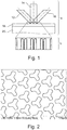
- Fig. 1a schematically shows an exposure to three coplanar beams 12, 14, 16.
- the three beams are distinct and coherent light beams, directed on the same region of a photosensitive resin 18 disposed on a substrate 20, at angles of different incidence.
- the three beams will interfere to form an interference pattern.
- the interference figure achieves a sort of masking of the resin 18, since it comprises areas of varying light intensity, resulting in areas exposed or not exposed to the resin.
- the interference figure allows spatially selective insolation of the resin 18, inducing a corresponding pattern therein.
- the Fig. 1b shows the insolation profile obtained in resin 18 after a single interference exposure to three coplanar beams whose relative intensities are different (here the intensity of the central beam represents half that of the lateral beams).
- the intensity of the central beam represents half that of the lateral beams.
- different patterns with limited symmetry can be obtained by modifying the exposure parameters, including: relative phase shifts between beams, relative intensities between beams, angles of incidence of the beams, exposure time, angle of rotation .
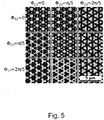
- the figure 5 shows a simulation of the different patterns with limited symmetry that can be obtained by varying the relative phases between the beams 12 and 14 (phase difference noted ⁇ 12 ) and the beams 14 and 16 noted (phase difference noted ⁇ 23 ).
- Steps 1, 3 and 4 are conventional and will therefore not be explained in detail (except in the context of an example below). They can be implemented with existing materials and devices.
- a substrate 44 On a sample holder 42, a substrate 44 has been placed, the upper surface 46 of which is covered with a film of photosensitive resin 48.
- the substrate 44 is for example made of silicon, but may be of any suitable material.
- the photosensitive resin 48 can also be of any suitable type, which will in particular be chosen as a function of the wavelength of the incident beams and of the desired resolution.
- a positive resin with a threshold for example of type S1813
- the type of resin is adapted to the wavelength which is used for its exposure.
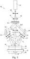
- Reference sign 50 denotes a laser source having a predetermined wavelength.
- the coherent light beam 52 produced by the source is first extended through a pair of lenses 54, before meeting a phase mask 56.
- the idea is to widen the source beam 52 so that it extends. over a large area of the mask, for example to reach a diameter of the order of 1 cm.
- the phase mask 56 serves to divide the source beam 52 into three beams of coplanar wave vectors 58.1, 58.2 and 58.3.
- the beam 58.2 is called “central” and the beams 58.1 and 58.2 are called “lateral” or “outer”.
- the phase mask 56 can be a conventional diffraction grating and a commercial phase mask can be used.
- a phase mask from the company IBSEN, having a size of 1 cm x 1 cm and a period of 490 nm designed for S-polarized light. With such a mask, the intensity of the central beam is equal to half of the other two.
- Each beam 58.1, 58.2 and 58.3 is advantageously spatially filtered by passing first through a lens 60 then an orifice 62 (pinhole), which allows a homogeneous distribution of intensity.
- a lens with a focal length of 7.5 cm and an orifice of 5 ⁇ m can be used.
- phase mask can be replaced by any device capable of separating the coherent light source into three beams of coplanar wave vectors.
- a diffraction grating could be used alternatively.
- the central beam 58.2 exits the phase mask 56 perpendicularly thereto, and therefore has a normal incidence on the upper face of the resin 48.
- Two mirrors 64 are used to make the lateral beams 58.1 and 58.3 converge towards the zone of. incidence of the central beam, so that the three beams interfere on the same part of the so-called “exposure surface” resin.
- the respective angles of incidence of the three beams 58.1, 58.2 and 58.3 are denoted ⁇ 1 , ⁇ 0 and ⁇ 2 .
- the angle ⁇ 0 between the central beam F2 and the upper surface of the resin is equal to 90 °.
- the angles ⁇ 1 and ⁇ 2 (angle with respect to the central beam F2) are generally between 5 and 70 °, in particular of the order of 20 °.
- the meeting of the three beams 58.1, 58.2 and 58.3 at the level of the exposure surface will therefore generate an interference pattern, which will make it possible to induce a pattern in the resin film 48.
- the interference comprises zones of varied light intensities, which will, depending on the sensitivity threshold of the resin, generate exposed zones of the resin or non-exposed zones, in accordance with the interference pattern.
- interference lithography is the ability to treat relatively large surfaces by a single exposure step, going with current technical means up to approximately 1 cm 2 , larger surfaces being possible with suitable optics and more powerful lasers.
- the conditions set out above are used to produce three exposures, in particular with a view to obtaining the patterns of stars with three branches. According to variants more exposures can be made, and other symmetrical geometric shapes obtained.
- a first exposure is carried out, referenced as the 0 ° position.
- a first rotation of the sample is carried out, in order to achieve a second exposure - 60 ° position.
- the sample is further rotated by 60 ° in the same direction (therefore by 120 ° with respect to the 0 ° position), in order to carry out a third exposure in the 120 ° position.
- the exposure conditions are the same for all three exposures.
- Rotation of the sample is preferred because it is easier to perform than rotation of the optical system.
- the sample holder is for example mounted on a swivel base 66 comprising a controlled electric motor. It will be noted that the pivoting of the substrate is preferably carried out along an axis of rotation R coincident with the axis F 2 of the central beam 58.2.
- the intensity of the beams it is possible to modulate the relative intensities.
- the outer beams have the same intensity and the intensity of the central beam is reduced, e.g. by 50%.
- phase modulation between the different beams makes it possible to vary the patterns, as seen for example in Fig. 5 .
- a silicon substrate 44 coated on its upper face with a photosensitive resin 48 (for reasons of simplicity, the same reference signs are used as in the figure Fig. 3 ).
- Silicon substrates having a thickness of 600-750 ⁇ m were cleaned for 5 min in an ultrasonic bath of acetone and isopropanol. The substrates were then dried and placed on a hot plate at 400 ° C to improve the adhesion between the silicon and the resin.
- the photosensitive resin chosen was a positive resin with a threshold, in particular an S1813 resin (Microchem company), sensitive to wavelengths of 405 nm and a resolution of 0.5 ⁇ m.
- the resin diluted to 50% in a solvent (Microposit EC) was deposited in a thin layer of 350 nm by means of a spin coater (30 s at 4000 rpm, acceleration 3000 rpm). The solvent was evaporated in an oven at 110 ° C.
- the substrate 44 thus prepared with its thin layer of photosensitive resin 48 was then placed in an optical system of the type of the Fig. 3 (equipped with a 450 nm laser) to undergo an exposure step comprising a triple interference exposure with three coplanar beams, in accordance with the present invention.
- Image a) shows the principle of an interference exposure, in which the three light beams 58.1, 58.2 and 58.3 produced by the optical system converge on the same part of the surface and interfere together.
- Three interference exposures of resin 48 were carried out, for angular positions of the substrate of 0 °, 60 ° and 120 °. Each exposure was carried out under the same conditions for the incident beams (intensity of the central beam is half that of the beams lateral), with a duration of a few tens of seconds, depending on the intensity of the laser beam exposing the sample.
- This exposure step therefore makes it possible to induce the pattern of the interference figure produced by the three coplanar beams, as represented by image b).
- the exposed areas i.e. in which the light intensity of the interference pattern was greater than the sensitivity threshold of the resin.
- the resin is developed to reveal the induced structure. Development was performed in an MF319 developer solution (MicroChem) for 30 s, followed by a water rinse.
- MF319 developer solution MocroChem
- Image d represents the deposition of gold by evaporation. After development of the resin, a 3 nm thick chromium adhesion layer was first preferably formed (not shown). Then a 50 nm layer of gold, designated 74, was deposited by thermal evaporation (at the rate of 1 nm / s).
- the last step aims to remove the sacrificial material, i.e. the resin, remaining on the substrate 44.
- the respective thicknesses of the sacrificial material (resin) and of the target material layer (gold) deposited on the latter will be adjusted, in a conventional manner. Indeed, if the resin thickness is too Importantly, the target material settles on the sides of the cutouts, which protects the underlying resin (image e, left).
- the thickness of resin 48 does not generally exceed three times the thickness of the layer 74 of gold.
- the shading phenomenon prevents the deposition of gold on the sides of the resin profile and therefore leads to a discontinuity of the gold layer (denoted 74.1) between the top of the resin and the gold layer (denoted 74.2) formed in the holes on the substrate 44. It is thus possible to chemically dissolve the resin 48 and thereby remove the metal 74.1 deposited on the latter. In the present example, the resin was dissolved with acetone.
- the upper face 46 of the substrate 44 only bears the desired metal nanostructures 74.2, here the three-branched gold nanostructures.
- the figure 6 shows an embodiment of an optical system 100 employing a truncated prism, allowing the implementation of the present method.
- a substrate 44 ' will be recognized, the upper surface 46' of which is covered with a film of photosensitive resin 48 '.
- the reference sign 102 designates a prism having an upper face 102.1 and a lower face 102.2 (or base) which are plane and parallel In the vertical plane of the figure, the prism 102 has a trapezoidal section: the base 102.2 is therefore wider than the upper face 102.1 and there are two opposite and symmetrical side faces 102.3 which join the two faces 102.1 and 102.2.
- a prism can typically be a right prism, in particular a Dove prism, which has been placed on a lateral face.
- the prism is in a transparent material in the light, typically in flint or crown glass for the visible or quartz in the UV.
- the coplanar light beams are generally indicated 104 and are directed, upstream of the prism, perpendicularly. on the resin surface.
- the central part of the beams attacks the planar upper surface 102.1 (parallel to its base 102.2 and to the upper resin surface) of the prism 102, passes through the latter and reaches the region of the resin surface with an angle of incidence of 90 °. This therefore forms the central beam F2.
- the coplanar beams 104 arrive on the inclined side faces of the prism 102.3 undergo a deviation (refraction) during their penetration into the prism, and arrive at the region of the resin surface with a angle of incidence different from 90 °.
- the lateral beams F1 and F3 are thus formed.
- phase and the intensity can advantageously be controlled by optical layers arranged on the side faces or at a distance.
- the phase of the side beams is controlled by means of thin optical layers 108 formed on the opposing side faces 102.3 of the prism.
- Optical density are positioned on the path of the end light beams, upstream of the prism, vertically to the side faces 102.3.
- Optical densities are generally absorbent layers, which may have a thickness of the order of a few nanometers in the case of metals or even a few tens of nanometers or even hundreds of nanometers if produced using doped oxides.
- these optical densities could be formed as thin layers directly on the side surfaces of the prism, e.g. above phase control layers 108.
- the prism 102 provides three coplanar beams which meet and interfere in the region of the base of the prism (indicated by dotted lines), near the surface of the resin 48 '. It is thus possible to insulate the resin 48 'by interference figures, in a manner similar to the optical system of the figure 3 .
- the use of the prism 102 in the optical system 100 allows great compactness. At the same time, it ensures the separation of the beams and their orientation, directing the lateral beams to make them interfere in the region of its base 102.2.
- the prism 102 can be placed directly on the photosensitive resin layer 48 '. It could also be slightly spaced. It will also be noted that with a transparent substrate of low thickness, the base of the prism can be placed against the rear face of the substrate (opposite to the face bearing the resin), in order to insulate the resin through the substrate. This is then an interference insolation by transmission.
Description
L'invention concerne généralement le domaine de la structuration de substrats par lithographie interférentielle, dite aussi lithographie holographique. De manière plus particulière, l'invention vise l'utilisation de la lithographie interférentielle pour la fabrication de méso- ou nanostructures métalliques sur des substrats, notamment en vue de la réalisation de capteurs pour la plasmonique.The invention generally relates to the field of the structuring of substrates by interference lithography, also known as holographic lithography. More particularly, the invention relates to the use of interference lithography for the manufacture of metallic meso- or nanostructures on substrates, in particular with a view to producing sensors for plasmonics.
Comme on le sait, le domaine de la plasmonique est basé sur l'interaction entre un faisceau lumineux et les électrons matériau à électrons libres (métal ou semi-conducteur fortement dopé), souvent sous forme de nanoparticules, nanostructures ou surfaces nanostructurées. Ces structures métalliques sont principalement utilisées dans le domaine des capteurs et détection des polluants mais également des capteurs de marqueurs biologiques de pathologies (protéines, etc.). Parmi les techniques les plus prometteuses, est la technique dite SERS pour Surface Enhanced Raman Spectroscopy qui permet de détecter les molécules présentes dans une solution qui se déposent sur une surface en exaltant leur réponse Raman ou encore le SEIRA pour Surface Enhanced InfraRed Absorption.As we know, the field of plasmonics is based on the interaction between a light beam and the free electron material electrons (metal or heavily doped semiconductor), often in the form of nanoparticles, nanostructures or nanostructured surfaces. These metal structures are mainly used in the field of sensors and detection of pollutants but also sensors of biological markers of pathologies (proteins, etc.). Among the most promising techniques, is the so-called SERS technique for Surface Enhanced Raman Spectroscopy, which detects molecules present in a solution that are deposited on a surface by enhancing their Raman response or even the SEIRA for Surface Enhanced InfraRed Absorption.
D'une manière générale, plusieurs techniques ont été utilisées pour la fabrication de nanoparticules métalliques (voir notamment
La lithographie optique. Cette technique typiquement employée en microélectronique consiste à illuminer une résine photosensible avec une source optique monochromatique à travers un masque qui a la forme des structures/particules souhaitées (résine positive), ou une forme complémentaire (résine négative). Elle est limitée en résolution à la fois par les propriétés de la résine, et par la longueur d'onde du faisceau utilisé. Les longueurs d'ondes utilisées aujourd'hui se situent dans l'UV profond (190 nm) ou EUV (12 nm) seraient compatibles avec les dimensions typiques de structures plasmoniques (50 nm), cependant le coût des instruments et des procédés est prohibitif pour la réalisation de grandes surfaces nanostructurées jetables (ou consommables) pour des capteurs plasmoniques et nécessite bien entendu la fabrication de masques spécifiques. Optical lithography. This technique typically employed in microelectronics consists in illuminating a photosensitive resin with a monochromatic optical source through a mask which has the shape of the desired structures / particles (positive resin), or a complementary shape (negative resin). It is limited in resolution both by the properties of the resin, and by the wavelength of the beam used. The wavelengths used today are in the deep UV (190 nm) or EUV (12 nm) would be compatible with the typical dimensions of plasmonic structures (50 nm), however the cost of instruments and methods is prohibitive. for the production of large disposable nanostructured surfaces (or consumables) for plasmonic sensors and of course requires the manufacture of specific masks.
La lithographie par nano-sphères. Ce procédé a été le premier utilisé pour réaliser des structures plasmoniques à forme contrôlée. Il consiste à auto-organiser des nano-sphères sur l'échantillon, suivi par une évaporation du métal souhaité et retrait des nano-sphères. On obtient des nanoparticules métalliques dans les interstices du réseau de nano-sphères et par conséquent les formes de structures obtenues sont limitées à des triangles typiquement. Cette technique est simple, compatible à grande échelle mais limitée par l'absence d'ordre à grande distance aux échelles microniques (10 à 20 fois typiquement la taille des billes). Lithography by nanospheres. This process was the first used to produce shape-controlled plasmon structures. It consists of self-organizing nano-spheres on the sample, followed by evaporation of the desired metal and removal of the nano-spheres. Metal nanoparticles are obtained in the interstices of the network of nanospheres and consequently the shapes of structures obtained are typically limited to triangles. This technique is simple, compatible on a large scale but limited by the absence of order at large distances on micron scales (typically 10 to 20 times the size of the beads).
La lithographie électronique. La résine (typiquement du PMMA) est exposée localement à l'aide d'un faisceau d'électrons. La résolution est de quelques nm. Combinée au procédé lift-off, cette technique permet un dépôt localisé de métal (après une étape de révélation de la résine). Comme pour la technique voisine d'écriture par faisceau d'ions focalisés, la vitesse d'écriture est lente. Cette technique est utilisée en SERS car elle permet un contrôle complet sur la forme et l'espacement entre les particules. Elle n'est cependant pas compatible à grande échelle avec des temps typiques d'exposition pour les plus rapides de 2h pour 1 mm2. Electronic lithography. The resin (typically PMMA) is exposed locally using an electron beam. The resolution is a few nm. Combined with the lift-off process, this technique allows a localized deposit of metal (after a step of revealing the resin). As with the related focused ion beam writing technique, the writing speed is slow. This technique is used in SERS because it allows complete control over the shape and spacing between particles. However, it is not compatible on a large scale with typical exposure times for the fastest of 2 hours for 1 mm 2 .
Lithographie interférentielle. La lithographie interférentielle consiste à créer une figure d'interférences à la surface d'un matériau photosensible. Cette technique est compatible avec une grande surface à structurer et permet la réalisation de motifs de forme et géométrie variées. Cette technique est limitée à la réalisation de structure périodique ou quasi-périodique avec un espacement minimal égal à la moitié de la longueur d'onde du laser. La taille des structures n'est par contre pas limitée et peut être ajustée en fonction de la dose et des propriétés de la résine. Il est possible cependant de diminuer l'espacement des structures en travaillant en immersion i.e. en changeant l'indice de réfraction du milieu. Notons encore que la lithographie interférentielle par l'utilisation de figure d'interférence permet d'obtenir potentiellement les structures les plus régulières réalisables sur de grandes surfaces. La limitation principale vient de la qualité des faisceaux laser étendus. Interferential lithography. Interferential lithography consists in creating an interference pattern on the surface of a photosensitive material. This technique is compatible with a large surface to be structured and allows the production of patterns of various shapes and geometry. This technique is limited to producing a periodic or quasi-periodic structure with a minimum spacing equal to half the wavelength of the laser. Size on the other hand, structures are not limited and can be adjusted depending on the dose and the properties of the resin. However, it is possible to reduce the spacing of the structures by working in immersion, ie by changing the refractive index of the medium. It should also be noted that interference lithography by the use of interference figures potentially makes it possible to obtain the most regular structures achievable over large surfaces. The main limitation comes from the quality of the extended laser beams.
On citera à titre d'exemple les documents suivants qui décrivent la lithographie interférentielle à deux et trois faisceaux :
Appliquée à la structuration de matériaux inorganiques, la technique de lithographie interférentielle est avant tout une technique de masquage et doit être combinée avec des techniques de transfert comme la gravure ou le procédé lift-off, comme pour les deux techniques précédentes.Applied to the structuring of inorganic materials, the interference lithography technique is above all a masking technique and must be combined with transfer techniques such as etching or the lift-off process, as for the two previous techniques.
Concernant plus spécifiquement les structures plasmoniques dans le domaine SERS, le
Cette structure en étoile proposée dans le
La méthode de fabrication décrite dans le
Il serait donc souhaitable de disposer d'une méthode de structuration rapide adaptée au domaine de la plasmonique, plus particulièrement pour la fabrication de structures à symétrie limitée, tel que des étoiles à trois branches.It would therefore be desirable to have a rapid structuring method suitable for the field of plasmonics, more particularly for the manufacture of structures with limited symmetry, such as stars with three branches.
La présente invention concerne un procédé de fabrication de structures à symétrie limitée par lithographie interférentielle comprenant une étape d'insolation par lithographie interférentielle d'un matériau photosensible disposé sur un substrat.The present invention relates to a method of manufacturing structures with limited symmetry by interference lithography comprising a step of exposure by interference lithography of a photosensitive material placed on a substrate.
Selon l'invention, l'étape d'insolation comprend au moins trois expositions interférentielles successives réalisées avec trois faisceaux lumineux coplanaires, émis par un système optique de sorte à interférer ensemble sur une même partie du matériau photosensible, dite surface d'exposition. Une rotation relative est réalisée entre le système optique et le substrat entre la première et la deuxième exposition interférentielle, puis entre la deuxième et la troisième exposition interférentielle.According to the invention, the exposure step comprises at least three successive interference exposures carried out with three coplanar light beams, emitted by an optical system so as to interfere together on the same part of the photosensitive material, called the exposure surface. A relative rotation is carried out between the optical system and the substrate between the first and the second interference exposure, then between the second and the third interference exposure.
Un mérite des présents inventeurs est d'avoir mis au point, de manière surprenante et non-prévisible, une étape d'insolation par lithographie interférentielle permettant de réaliser des structures géométriques complexes à symétrie limitée, notamment des étoiles à trois branches.One merit of the present inventors is to have developed, in a surprising and unpredictable manner, an exposure step by interference lithography making it possible to produce complex geometric structures with limited symmetry, in particular stars with three branches.
Jusqu'à présent, comme indiqué dans la partie relative à l'état de la technique, la lithographie interférentielle avait été utilisée pour la fabrication de structures simples, notamment des particules ou trous cylindriques. Des structures du type étoile d'or à trois branches, très utiles pour la plasmonique, avaient été fabriquées par lithographie électronique, comme décrit dans le
La présente invention va donc permettre la fabrication de masse de substrats avec des méso ou nanostructures à symétrie limitée, en profitant des avantages de la lithographie interférentielle : facilité de mise en œuvre, vitesse de production rapide, traitement de larges surfaces...The present invention will therefore allow the mass manufacture of substrates with meso or nanostructures with limited symmetry, taking advantage of the advantages of interference lithography: ease of implementation, rapid production speed, treatment of large surfaces, etc.
Dans la présente, le terme « symétrie limitée » est utilisé pour se distinguer d'objets tels que des plots. En particulier, on entend par « méso ou nanostructures à symétrie limitée » des structures comprenant des méso ou nano-particules, connexes ou non, présentant une symétrie d'ordre n, où n≥3. C'est-à-dire que la particule est invariante par rotation autour d'un axe perpendiculaire à la surface du substrat d'un angle 2Pi/n, où n est supérieur ou égal à trois. Avec la terminologie des « groupes de papier peint », c'est-à-dire des groupes mathématiques constitués par l'ensemble des symétries d'un motif bidimensionnel périodique, le terme « symétrie limitée » représente les groupes p6, p6m, p3, p31m et p3m1. Ces motifs ne sont pas nécessairement des particules indépendantes, mais sont une structuration nanométrique ou micrométrique des motifs périodiques. Rappelons que nous entendons ici par nanométrique des objets de taille inférieur à 100nm, par mesoscopique des objets de taille comprise entre 100 nm et 1 micron et micronique des objets de taille supérieure au micron.In the present, the term "limited symmetry" is used to distinguish itself from objects such as studs. In particular, the term “meso or nanostructures with limited symmetry” is understood to mean structures comprising meso or nanoparticles, connected or not, exhibiting symmetry of order n, where n≥3. That is, the particle is invariant by rotation around an axis perpendicular to the surface of the substrate at an angle 2Pi / n, where n is greater than or equal to three. With the terminology of "wallpaper groups", that is to say mathematical groups formed by the set of symmetries of a periodic two-dimensional pattern, the term "limited symmetry" represents the groups p6, p6m, p3, p31m and p3m1. These patterns are not necessarily independent particles, but are a nanometric or micrometric structuring of the periodic patterns. Remember that we mean here by nanometric objects of size less than 100nm, by mesoscopic objects of size between 100 nm and 1 micron and micron size of objects greater than one micron.
Le présent procédé est bien entendu compatible avec les technologies conventionnelles de lithographie. En pratique, le procédé comprendra généralement : une étape de préparation du substrat, dans laquelle il est recouvert d'un film de résine photosensible ; l'étape d'insolation conforme à l'invention ; une étape de développement de la résine, afin de libérer sélectivement les zones insolées ou non-insolées (selon que la résine est positive ou négative) par la figure d'interférence ; et une étape dite de transfert, dans laquelle on réalise un dépôt métallique sur la résine/substrat, par exemple suivi soit d'une gravure ou d'un lift-off.The present process is of course compatible with conventional lithography technologies. In practice, the method will generally comprise: a step of preparing the substrate, in which it is covered with a film of photosensitive resin; the exposure step according to the invention; a resin development step, in order to selectively release the exposed or non-exposed areas (depending on whether the resin is positive or negative) by the interference pattern; and a so-called transfer step, in which a metallic deposit is carried out on the resin / substrate, for example followed either by etching or by a lift-off.
A noter que les techniques de transfert type gravure ou lift off sont surtout requises pour la structuration de surface des substrats/matériaux inorganiques.It should be noted that transfer techniques such as etching or lift off are especially required for the surface structuring of substrates / inorganic materials.
De manière générale, on pourra jouer sur différents paramètres opératoires pour faire varier les formes géométriques des méso ou nanostructures fabriquées, parmi lesquels notamment : intensité totale des faisceaux, intensités relatives des faisceaux, phases relatives des faisceaux, angles d'incidence des faisceaux, angles de rotation de l'échantillon, durée d'exposition.In general, we can play on different operating parameters to vary the geometric shapes of the meso or nanostructures manufactured, including in particular: total intensity of the beams, relative intensities of the beams, relative phases of the beams, angles of incidence of the beams, angles sample rotation, exposure time.
De préférence, on contrôle les intensités relatives des faisceaux. Par exemple, les faisceaux extérieurs ont la même intensité et l'intensité du faisceau central est réduite, par ex. de 50%.Preferably, the relative intensities of the beams are controlled. For example, the outer beams have the same intensity and the intensity of the center beam is reduced, e.g. by 50%.
Pour un bon contrôle de la géométrie des structures sur la surface exposée, on contrôle avantageusement la phase de chacun des faisceaux, par exemple au moyen d'un dispositif de contrôle de phase. Tout type de dispositif de contrôle de phase approprié peut être utilisé, on citera à titre d'exemple un miroir posé sur un cristal piézoélectrique. La modulation de phase est notamment effectuée pour former des motifs d'étoiles ou de points dans la résine photosensible. Sans contrôle la de phase, la technique reste également intéressante car elle aboutit à des zones de structures différentes qui potentiellement résonnent à des longueurs d'onde différente. Dans le cadre de capteurs plasmoniques, cela permet donc d'envisager une détection combinée de plusieurs espèces.For good control of the geometry of the structures on the exposed surface, the phase of each of the beams is advantageously controlled, for example by means of a phase control device. Any type of suitable phase control device can be used, for example a mirror placed on a piezoelectric crystal. The phase modulation is in particular carried out to form patterns of stars or dots in the photosensitive resin. Without phase control, the technique also remains interesting because it results in zones of different structures which potentially resonate with different wavelengths. In the context of plasmonic sensors, this therefore makes it possible to envisage a combined detection of several species.
Comme on le comprendra, lors d'une exposition interférentielle, la résine reçoit une certaine dose d'insolation, fonction de la combinaison des différents paramètres mentionnés ci-dessus. Selon les variantes, les doses d'insolation peuvent être identiques ou différentes entre chaque exposition interférentielle. Le nombre expositions interférentielles peut également être supérieur à trois, par exemple avec un pas angulaire de 180°/n (n étant le nombre d'expositions). Des expositions avec des pas différents sont possibles, par exemple, 30° puis 60° et enfin 120°.As will be understood, during an interference exposure, the resin receives a certain dose of insolation, depending on the combination of the various parameters mentioned above. According to the variants, the insolation doses may be identical or different between each interference exposure. The number of interference exposures can also be greater than three, for example with an angular pitch of 180 ° / n (n being the number of exposures). Exposures with different pitches are possible, for example, 30 ° then 60 ° and finally 120 °.
Selon un mode de réalisation, les faisceaux lumineux coplanaires sont émis par un système optique qui produit : un faisceau central, de préférence ayant un angle d'incidence normal par rapport au plan du substrat, et deux faisceaux latéraux (de phase relative avec le faisceau central fixée), de part et d'autre du faisceau central, tous les trois dans un même plan, les faisceaux latéraux ayant un angle d'incidence inférieur à 90° par rapport au plan moyen du substrat (respectivement de la couche de matériau photosensible), les trois faisceaux lumineux étant dirigés sensiblement sur la surface d'exposition du matériau photosensible afin de produire une figure d'interférences.According to one embodiment, the coplanar light beams are emitted by an optical system which produces: a central beam, preferably having a normal angle of incidence with respect to the plane of the substrate, and two lateral beams (of relative phase with the beam central fixed), on either side of the central beam, all three in the same plane, the lateral beams having an angle of incidence less than 90 ° with respect to the mean plane of the substrate (respectively of the layer of photosensitive material ), the three light beams being directed substantially on the exposure surface of the photosensitive material in order to produce an interference pattern.
L'angle d'incidence des faisceaux latéraux techniquement peut être compris entre 5° et 70° (angle par rapport à la normale à la surface).The angle of incidence of the lateral beams technically can be between 5 ° and 70 ° (angle with respect to the normal to the surface).
Selon les variantes, on pourra faire varier l'angle de rotation du substrat en fonction de la taille des structures désirées. La rotation est typiquement réalisée dans le plan du substrat. Préférablement, pour des géométries en étoile on pivote le substrat de 60° entre chaque exposition interférentielle (en partant d'une position initiale 0°) ; l'étape d'insolation comprend donc trois expositions dans des positions à 0°, 60° et 120°. En pratique, la rotation relative du substrat est préférablement réalisée par déplacement-rotation du substrat.According to the variants, it is possible to vary the angle of rotation of the substrate as a function of the size of the desired structures. The rotation is typically performed in the plane of the substrate. Preferably, for star geometries, the substrate is rotated by 60 ° between each interference exposure (starting from an initial position of 0 °); the exposure step therefore comprises three exposures in positions at 0 °, 60 ° and 120 °. In practice, the relative rotation of the substrate is preferably carried out by displacement-rotation of the substrate.
Comme on le comprendra, pour des angles différents, on pourra avoir un nombre d'expositions différents. Par exemple, pour un angle de 45° on réalise quatre expositions à 45, 90 et 135°. En outre, les paramètres de chaque exposition peuvent aussi différer.As will be understood, for different angles, we can have a number of different exposures. For example, for an angle of 45 ° we realize four exposures at 45, 90 and 135 °. In addition, the settings for each exposure may also differ.
Le substrat sera choisi en fonction des applications, il peut s'agir de silicium, de verre (tranparent dans l'infrarouge et/ou le visible et/ou l'ultraviolet), de chalcogénures, ou de systèmes structurés tels que des guides d'ondes sur lesquels on vient structurer des nanoparticules. Les méso ou nanoparticules à symétrie limitées sont fabriquées dans des matériaux adaptés au processus de transfert choisi, il peut s'agir de métaux (or, argent, aluminium, chrome, cuivre notamment) en dépôt simple ou des couches de métaux différents (or sur couche d'accroché de chrome, par exemple) ou semi-conducteurs intrinsèques ou dopés (incluant ceux à haut gap tel que le ZnO), ou encore d'oxydes via des procédés solgel.The substrate will be chosen according to the applications, it can be silicon, glass (transparent in the infrared and / or the visible and / or the ultraviolet), chalcogenides, or structured systems such as guides of waves on which we come to structure nanoparticles. Meso or nanoparticles with limited symmetry are made of materials suitable for the chosen transfer process, they can be metals (gold, silver, aluminum, chromium, copper in particular) in simple deposit or layers of different metals (gold on bond layer of chromium, for example) or intrinsic or doped semiconductors (including those with a high gap such as ZnO), or of oxides via solgel processes.
De manière plus particulière, le présent procédé permet la fabrication de structures comprenant des méso ou nano-particules présentant une symétrie d'ordre Cn, où n≥3 (comme noté en théorie des groupes). C'est-à-dire que la particule est invariante par rotation autour d'un axe perpendiculaire à la surface du substrat d'un angle 2Pi/n, où n est supérieur ou égal à trois.More particularly, the present process allows the fabrication of structures comprising meso or nano-particles exhibiting a symmetry of order Cn, where n≥3 (as noted in group theory). That is, the particle is invariant by rotation around an axis perpendicular to the surface of the substrate at an angle 2Pi / n, where n is greater than or equal to three.
En considération des applications à la plasmonique, le présent procédé permet la fabrication de structures constituées de nanoparticules ou groupes de nanoparticules présentant une forme (pour les nanoparticules) ou une disposition (pour les groupes de particules) ayant un axe de symétrie perpendiculaire à ladite face de type Cn où n est supérieur ou égal à trois, de façon à permettre une forte exaltation dudit faisceau à proximité de ladite face, lors de la mise en œuvre du capteur fabriqué avec ce type de structure. La forme étant adaptée aux résonances plasmoniques aux fréquences désirées.In consideration of applications to plasmonics, the present process allows the fabrication of structures made up of nanoparticles or groups of nanoparticles having a shape (for nanoparticles) or an arrangement (for groups of particles) having an axis of symmetry perpendicular to said face of type Cn where n is greater than or equal to three, so as to allow a strong enhancement of said beam near said face, during the implementation of the sensor manufactured with this type of structure. The shape being adapted to plasmonic resonances at the desired frequencies.
Les structures à symétrie limitée de type étoiles sont ici particulièrement intéressantes, car un effet d'amplification de champ est attendu quelle que soit la polarisation incidentes. Ce type de structures trouve des applications dans le domaine de la détection amplifiée de type Raman (SERS) ou absorption infrarouge type SEIRA.The star type structures with limited symmetry are particularly interesting here, because a field amplification effect is expected regardless of the incident polarization. This type of structure finds applications in the field of amplified detection of Raman type (SERS) or infrared absorption of SEIRA type.
Toujours dans le cadre de la plasmonique, le présent procédé est préférablement utilisé pour la fabrication de structures comprenant des nanoparticules présentant dans leur majorité une forme en étoile ayant au moins trois branches. Les nanoparticules peuvent être métalliques et/ou semi conductrices. Elles présentent préférentiellement une dimension comprise entre le nanomètre et quelques dizaines de micromètres. En outre en fonction du réseau dans lequel lesdites nanoparticules sont incluses, on peut avoir un pavage régulier ou quasi-cristallin. Le substrat peut être constitué d'un matériau transparent aux longueurs d'onde des ultraviolets, du visible et/ou de l'infrarouge. La dimension desdites nanoparticules ou groupes de nanoparticules pourra être choisie de façon à ce qu'elles soient accordées sur une longueur d'onde du faisceau incident utilisé pour la lecture du capteur. En général, les nanoparticules sont disposées sur au moins une partie du substrat, selon un pavage régulier ou quasi cristallin ou aléatoire.Still in the context of plasmonics, the present process is preferably used for the manufacture of structures comprising nanoparticles mostly having a star shape having at least three branches. The nanoparticles can be metallic and / or semi-conductive. They preferably have a dimension between one nanometer and a few tens of micrometers. In addition, depending on the network in which said nanoparticles are included, it is possible to have a regular or quasi-crystalline tiling. The substrate can be made of a material transparent to ultraviolet, visible and / or infrared wavelengths. The dimension of said nanoparticles or groups of nanoparticles can be chosen so that they are tuned to a wavelength of the incident beam used for reading the sensor. In general, the nanoparticles are placed on at least part of the substrate, in a regular or quasi-crystalline or random tiling.
Les substrats fabriqués selon le présent procédé peuvent être employés pour la détection et/ou la mesure de molécules et/ou de cibles de type chimique, biochimique ou biologique. De tels substrats seront avantageusement employés pour la détection et/ou la mesure de molécules et/ou de supra-molécules et/ou de particules dans un milieu liquide (souvent aqueux) et/ou biologique et/ou encore dans des fluides corporels tels que le sang. Selon ce dernier type d'application, des virus ou bactéries pourront être identifiés, y compris au niveau individuel.The substrates produced according to the present method can be used for the detection and / or measurement of molecules and / or targets of chemical, biochemical or biological type. Such substrates will advantageously be used for the detection and / or measurement of molecules and / or supra-molecules and / or particles in a liquid (often aqueous) and / or biological medium and / or also in bodily fluids such as the blood. According to the latter type of application, viruses or bacteria can be identified, including at the individual level.
Selon un autre aspect, l'invention concerne aussi un système optique particulièrement adapté pour la fabrication de structures à symétrie limitée par lithographie interférentielle, comprenant :
- un porte échantillon ;
- une source de lumière cohérente émettant un faisceau lumineux source ;
- des moyens pour former, à partir du faisceau source, trois faisceaux lumineux coplanaires dirigés sur une surface d'exposition d'une résine photosensible recouvrant un substrat de sorte à interférer ; et
- des moyens pour faire pivoter le porte échantillon afin de réaliser plusieurs expositions interférentielles de la résine.
- a sample holder;
- a coherent light source emitting a source light beam;
- means for forming, from the source beam, three coplanar light beams directed on an exposure surface of a photosensitive resin covering a substrate so as to interfere; and
- means for rotating the sample holder in order to achieve several interference exposures of the resin.
Le système est remarquable en ce que les moyens pour former le faisceau comprennent un prisme comprenant une face inférieure et une face supérieure planes et parallèles et deux faces latérales opposés obliques, la face inférieure du prisme étant positionnée à proximité ou en contact d'un substrat recouvert d'une couche de résine photosensible lors de l'utilisation, alors que le faisceau lumineux source est dirigé perpendiculaire à la face inférieure du prisme, et tombe sur la face supérieure du prisme ainsi que sur deux face latérales obliques.The system is remarkable in that the means for forming the beam comprise a prism comprising a lower face and an upper face which are plane and parallel and two opposite oblique lateral faces, the lower face of the prism being positioned near or in contact with a substrate. covered with a layer of photosensitive resin during use, while the source light beam is directed perpendicular to the lower face of the prism, and falls on the upper face of the prism as well as on two oblique side faces.
Le prisme est configuré de sorte que les faisceaux pénétrant par la face supérieure arrivent avec une incidence normale sur la face inférieure et les faisceaux lumineux pénétrant par lesdites faces latérales obliques convergent vers la face inférieure du prisme pour interférer.The prism is configured so that the beams penetrating from the upper face arrive with a normal incidence on the lower face and the light beams penetrating through said oblique side faces converge towards the lower face of the prism to interfere.
Ce système optique est particulièrement bien adapté pour la mise en œuvre du procédé décrit ci-avant. Le prisme tronqué confère au système une grande compacité, réduisant le nombre de pièces à un minimum. En outre, le prisme tronqué agit comme séparateur, formant trois faisceaux coplanaires distincts, tout en dirigeant ces faisceaux de manière à les faire converger à la base du prisme pour interférer. Enfin, dans un environnement aux conditions simples à contrôler (notamment stabilité raisonnable de la température et des supports mécaniques), les phases relatives des trois faisceaux restent suffisamment fixées (contrôlées) pour assurer la figure d'interférences voulues.This optical system is particularly well suited for implementing the method described above. The truncated prism makes the system very compact, reducing the number of parts to a minimum. Additionally, the truncated prism acts as a splitter, forming three distinct coplanar beams, while directing these beams to converge at the base of the prism to interfere. Finally, in an environment with conditions that are easy to control (in particular reasonable stability of the temperature and of the mechanical supports), the relative phases of the three beams remain sufficiently fixed (controlled) to ensure the desired interference pattern.
De préférence, une couche d'adaptation d'épaisseur est déposée sur chacune ou une des desdites faces latérales opposées du prisme pour contrôler la phase relative des faisceaux lumineux.Preferably, a thickness matching layer is deposited on each or one of said opposite side faces of the prism to control the relative phase of the light beams.
Une densité optique est positionnée sur le chemin des faisceaux lumineux tombant sur les faces latérales, ou sur le chemin des faisceaux lumineux tombant sur la face tronquée du prisme, afin d'atténuer leur intensité, ladite densité optique pouvant prendre la forme d'une lame positionnée à distance du prisme ou bien d'une couche formée sur le prisme, respectivement sur ladite couche d'adaptation d'épaisseur.An optical density is positioned on the path of the light beams falling on the lateral faces, or on the path of the light beams falling on the truncated face of the prism, in order to attenuate their intensity, said optical density being able to take the form of a plate positioned at a distance from the prism or else from a layer formed on the prism, respectively on said thickness adaptation layer.
D'autres particularités et caractéristiques de l'invention ressortiront de la description détaillée d'au moins un mode de réalisation avantageux présenté ci-dessous, à titre d'illustration, en se référant aux dessins annexés. Ceux-ci montrent :
-
Figure 1 : un schéma de principe représentant une exposition à 3 faisceaux coplanaires ; -
Figure 2 : une image MEB de structures d'étoiles à trois branches en or (après lift off) obtenues sur un substrat silicium au moyen du présent procédé ; -
Figure 3 : est un schéma de principe d'un système optique utilisé pour la mise en œuvre du présent procédé ; -
Figure 4 : est un schéma illustrant par étapes un mode de réalisation du présent procédé de lithographie avec transfert par le process de lift-off ; -
Figure 5 : est un tableau représentant diverses formes (simulation) de méso- ou nanostructures pouvant être obtenues par le présent procédé ; et -
Figure 6 : est un schéma de schéma de principe d'un autre système optique utilisé pour la mise en œuvre du présent procédé.
-
Figure 1 : a schematic diagram representing an exposure to 3 coplanar beams; -
Figure 2 : a SEM image of structures of stars with three gold branches (after lift off) obtained on a silicon substrate by means of the present method; -
Figure 3 : is a block diagram of an optical system used for implementing the present method; -
Figure 4 : is a diagram illustrating in stages an embodiment of the present lithography process with transfer by the lift-off process; -
Figure 5 : is a table representing various forms (simulation) of meso- or nanostructures obtainable by the present method; and -
Figure 6 : is a block diagram diagram of another optical system used for the implementation of the present method.
La présente invention porte sur l'utilisation de la lithographie interférentielle à trois faisceaux coplanaires avec expositions multiples pour la réalisation de structures à symétrie limitée, comme par exemple la réalisation d'étoiles à 3 branches obtenues par triple exposition.The present invention relates to the use of interference lithography with three coplanar beams with multiple exposures for the realization of structures with limited symmetry, such as for example the realization of stars with 3 branches obtained by triple exposure.
Sur la
La
Mais on appréciera qu'en effectuant plusieurs expositions interférentielles, avec rotation du substrat, ces lignes disparaissent et l'on obtient des motifs de symétrie limitée.However, it will be appreciated that by carrying out several interference exposures, with rotation of the substrate, these lines disappear and patterns of limited symmetry are obtained.
De manière surprenante et non-prévisible, les présents inventeurs ont en effet découvert qu'une triple exposition avec trois faisceaux coplanaires, tel qu'illustré à la
De manière générale, on pourra obtenir différents motifs à symétrie limitée en modifiant les paramètres d'exposition, parmi lesquels : décalages de phases relatives entre faisceaux, intensités relatives entre faisceaux, angles d'incidence des faisceaux, durée d'exposition, angle de rotation.In general, different patterns with limited symmetry can be obtained by modifying the exposure parameters, including: relative phase shifts between beams, relative intensities between beams, angles of incidence of the beams, exposure time, angle of rotation .
A titre d'exemple, la
Pour la réalisation de méso- ou nanostructures métalliques à symétrie limitée, le principe d'une exposition interférentielle multiple à trois faisceaux coplanaires est combiné avec les étapes conventionnelles des procédés lithographiques. Le processus de réalisation complet comprendra donc typiquement étapes de :
- 1. Préparation du substrat: dépôt du matériau sacrificiel, i.e. une résine photosensible, sur la surface du substrat ;
- 2. Insolation du substrat (que l'on peut également appeler étape de masquage) : multiple exposition interférentielle du substrat à trois faisceaux coplanaires, avec rotation du substrat, pour exposer sélectivement des zones de résines conformément à la figures d'interférences créée sur la résine ;
- 3. Développement de la résine pour libérer sélectivement des parties définies par l'étape d'insolation ;
- 4. Fabrication de la structure : on dépose le métal selon les motifs formés dans la résine, par un procédé approprié, dont par exemple lift-off ou gravure.
- 1. Preparation of the substrate: deposition of the sacrificial material, ie a photosensitive resin, on the surface of the substrate;
- 2. Insolation of the substrate (which can also be called the masking step): multiple interference exposure of the substrate to three coplanar beams, with rotation of the substrate, to selectively expose areas of resins in accordance with the interference figures created on the diagram. resin;
- 3. Development of the resin to selectively release parts defined by the exposure step;
- 4. Manufacture of the structure: the metal is deposited according to the patterns formed in the resin, by an appropriate process, including for example lift-off or etching.
Les étapes 1, 3 et 4 sont classiques et ne seront donc pas expliquées en détail (sauf dans le cadre d'un exemple ci-dessous). Elles peuvent être mises en œuvre avec les matériaux et appareils existants.
On va maintenant décrire un système optique 40 permettant de réaliser une étape d'insolation conforme à l'invention, lequel est représenté schématiquement en
Sur un porte échantillon 42 on a placé un substrat 44 dont la surface supérieure 46 est couverte d'un film de résine photosensible 48. Le substrat 44 est par exemple en silicium, mais peut être en tout matériau approprié. La résine photosensible 48 peut également être de tout type approprié, qui sera notamment choisi en fonction de la longueur d'onde des faisceaux incidents et de la résolution souhaitée. En vue d'un transfert avec le procédé lift-off, on utilisera avantageusement une résine positive avec seuil (par exemple de type S1813). Classiquement, le type de résine est adapté à la longueur d'onde qui est utilisée pour son insolation.On a
Le signe de référence 50 désigne une source laser ayant une longueur d'onde prédéterminée. Le faisceau de lumière cohérente 52 produit par la source est d'abord étendu à travers une paire de lentilles 54, avant de rencontrer un masque de phase 56. L'idée est d'élargir le faisceau source 52 afin qu'il s'étende sur une grande surface du masque, par exemple pour atteindre un diamètre de l'ordre de 1 cm.
Le masque de phase 56 sert à diviser le faisceau source 52 en trois faisceaux de vecteurs d'onde coplanaires 58.1, 58.2 et 58.3. Le faisceau 58.2 est dit « central » et les faisceaux 58.1 et 58.2 sont dits « latéraux » ou « extérieurs ». Le masque de phase 56 peut être un réseau de diffraction classique et on pourra employer un masque de phase du commerce. A titre d'exemple, on peut citer un masque de phase de la société IBSEN, ayant une taille de 1 cm x 1 cm et une période 490 nm conçu pour la lumière polarisée S. Avec un tel masque, l'intensité du faisceau central est égale à la moitié des deux autres. Chaque faisceau 58.1, 58.2 et 58.3 est avantageusement filtré spatialement en passant d'abord au travers d'une lentille 60 puis un orifice 62 (pinhole), ce qui permet une distribution homogène d'intensité. Par exemple, on peut employer une lentille de focale de 7.5 cm et un orifice de 5 µm.The
On notera que le masque de phase peut être substitué par tout dispositif apte à séparer la source de lumière cohérente en trois faisceaux de vecteurs d'onde coplanaires. On pourra par exemple employer alternativement un réseau de diffraction.It will be noted that the phase mask can be replaced by any device capable of separating the coherent light source into three beams of coplanar wave vectors. For example, a diffraction grating could be used alternatively.
Le faisceau central 58.2 sort du masque de phase 56 perpendiculairement à celui-ci, et a donc une incidence normale sur la face supérieure de la résine 48. Deux miroirs 64 sont utilisés pour faire converger les faisceaux 58.1 et 58.3 latéraux vers la zone d'incidence du faisceau central, de sorte que les trois faisceaux interfèrent sur une même partie de la résine dite « surface d'exposition ». Les angles d'incidence respectifs des trois faisceaux 58.1, 58.2 et 58.3 sont notés θ1, θ0 et θ2. L'angle α0 entre le faisceau central F2 et la surface supérieure de la résine vaut 90°. Les angles θ1 et θ2 (angle par rapport au faisceau central F2) sont généralement entre 5 et 70°, en particulier de l'ordre de 20°.The central beam 58.2 exits the
La rencontre des trois faisceaux 58.1, 58.2 et 58.3 au niveau de la surface d'exposition va donc générer une figure d'interférences, qui va permettre d'induire un motif dans le film de résine 48. Comme on le comprendra, la figure d'interférence comprend des zones d'intensités lumineuses variées, qui vont, selon le seuil de sensibilité de la résine, engendrer des zones insolées de la résine ou des zones non-insolées, conformément au motif d'interférences.The meeting of the three beams 58.1, 58.2 and 58.3 at the level of the exposure surface will therefore generate an interference pattern, which will make it possible to induce a pattern in the
L'intérêt de la lithographie interférentielle est ici la capacité de traiter des surfaces relativement grandes par une seule étape d'insolation, allant avec les moyens techniques actuels jusqu'à environ 1 cm2, de plus grandes surfaces étant possibles avec une optique adaptée et des lasers plus puissants.The advantage of interference lithography here is the ability to treat relatively large surfaces by a single exposure step, going with current technical means up to approximately 1 cm 2 , larger surfaces being possible with suitable optics and more powerful lasers.
Les conditions exposées ci-avant sont utilisées pour réaliser trois expositions, notamment en vue d'obtenir les motifs d'étoiles à trois branches. Selon les variantes davantage d'expositions peuvent être réalisées, et d'autres formes géométriques symétriques obtenues.The conditions set out above are used to produce three exposures, in particular with a view to obtaining the patterns of stars with three branches. According to variants more exposures can be made, and other symmetrical geometric shapes obtained.
Dans le cadre de la triple exposition interférentielle, une première exposition est réalisée, référencée en tant que position 0°. Puis l'on opère une première rotation de l'échantillon de 60° dans son plan, pour réaliser une deuxième exposition - position 60°. Enfin on tourne encore l'échantillon de 60° dans le même sens (donc de 120° par rapport à la position 0°), pour réaliser une troisième exposition en position 120°. Pour cet exemple, les conditions d'exposition sont les mêmes pour les trois expositions.In the context of the triple interference exposure, a first exposure is carried out, referenced as the 0 ° position. Then a first rotation of the sample by 60 ° in its plane is carried out, in order to achieve a second exposure - 60 ° position. Finally, the sample is further rotated by 60 ° in the same direction (therefore by 120 ° with respect to the 0 ° position), in order to carry out a third exposure in the 120 ° position. For this example, the exposure conditions are the same for all three exposures.
La rotation de l'échantillon est préférée car elle est plus simple à réaliser que la rotation du système optique. Le porte échantillon est par exemple monté sur un socle pivotant 66 comprenant un moteur électrique piloté. On notera que le pivotement du substrat se fait de préférence selon un axe de rotation R confondu avec l'axe F2 du faisceau central 58.2.Rotation of the sample is preferred because it is easier to perform than rotation of the optical system. The sample holder is for example mounted on a
En pratique, on pourra jouer sur différents paramètres opératoires pour faire varier les formes géométriques des nanostructures fabriquées, parmi lesquels notamment : intensités des faisceaux, phases des faisceaux, angle d'incidence des faisceaux, angles de rotation de l'échantillon, durée d'exposition.In practice, we can play on different operating parameters to vary the geometric shapes of the nanostructures manufactured, including in particular: beam intensities, beam phases, beam incidence angle, sample rotation angles, duration of exposure.
Concernant l'intensité des faisceaux, on pourra moduler les intensités relatives. De préférence, les faisceaux extérieurs ont la même intensité et l'intensité du faisceau central est réduite, par ex. de 50%.Concerning the intensity of the beams, it is possible to modulate the relative intensities. Preferably, the outer beams have the same intensity and the intensity of the central beam is reduced, e.g. by 50%.
Concernant les phases des faisceaux, celles-ci peuvent être laissée libres. Il est toutefois préférable de contrôler les phases respectives des faisceaux, par ex. au moyen d'un contrôleur de phase sur chaque faisceau, pour mieux maitriser la géométrie du motif fabriqué sur la totalité de la surface exposée. Par ailleurs, la modulation de phase entre les différents faisceaux permet de faire varier les motifs, comme vu par exemple en
On va maintenant décrire, à l'aide de la
En se référant à la
La résine photosensible choisie était une résine positive avec seuil, notamment une résine S1813 (société Microchem), sensible aux longueurs d'onde de 405 nm et une résolution de 0,5 µm. La résine, diluée à 50% dans un solvant (Microposit EC) a été déposée en une couche mince de 350 nm au moyen d'un spin coater (30 s à 4 000 trs/min, accélération 3 000 trs/s). Le solvant a été évaporé dans un four à 110°C.The photosensitive resin chosen was a positive resin with a threshold, in particular an S1813 resin (Microchem company), sensitive to wavelengths of 405 nm and a resolution of 0.5 μm. The resin, diluted to 50% in a solvent (Microposit EC) was deposited in a thin layer of 350 nm by means of a spin coater (30 s at 4000 rpm, acceleration 3000 rpm). The solvent was evaporated in an oven at 110 ° C.
Le substrat 44 ainsi préparé avec sa couche mince de résine photosensible 48 a ensuite été placé dans un système optique du type de la
Cette étape d'insolation permet donc d'induire le motif de la figure d'interférence produite par les trois faisceaux coplanaires, comme représenté par l'image b). Les zones insolées (i.e. dans lesquelles l'intensité lumineuse de la figure d'interférence était supérieure au seuil de sensibilité de la résine) sont désignées 70.This exposure step therefore makes it possible to induce the pattern of the interference figure produced by the three coplanar beams, as represented by image b). The exposed areas (i.e. in which the light intensity of the interference pattern was greater than the sensitivity threshold of the resin) are designated 70.
Après l'étape d'insolation, la résine est développée pour révéler la structure induite. Le développement a été réalisé dans une solution de développeur MF319 (MicroChem) pendant 30 s, suivi d'un rinçage à l'eau.After the exposure step, the resin is developed to reveal the induced structure. Development was performed in an MF319 developer solution (MicroChem) for 30 s, followed by a water rinse.
Puisqu'il s'agit d'une résine positive, le développement révèle des trous 72 correspondant aux formes d'étoiles à trois branches désirées, symbolisé par l'image c). Dans le cadre du procédé lift-off, les trous formés dans la résine s'étendent jusqu'à la face supérieure 46 du substrat 44.Since it is a positive resin, the development reveals
L'image d) représente le dépôt d'or par évaporation. Après développement de la résine, on a d'abord préférentiellement formé une couche d'adhésion en Chrome de 3 nm d'épaisseur (non représentée). Puis une couche d'or de 50 nm, désignée 74, a été déposée par évaporation thermique (à la vitesse de 1 nm/s).Image d) represents the deposition of gold by evaporation. After development of the resin, a 3 nm thick chromium adhesion layer was first preferably formed (not shown). Then a 50 nm layer of gold, designated 74, was deposited by thermal evaporation (at the rate of 1 nm / s).
Conformément au procédé lift-off, la dernière étape vise à enlever le matériau sacrificiel, i.e. la résine, restant sur le substrat 44.In accordance with the lift-off process, the last step aims to remove the sacrificial material, i.e. the resin, remaining on the
Pour permettre le lift-off, on ajustera, de manière classique, les épaisseurs respectives du matériau sacrificiel (résine) et de la couche de matériau cible (or) déposée sur cette dernière. En effet, si l'épaisseur de résine est trop importante, le matériau cible se dépose sur les flancs des découpes, ce qui protège la résine sous-jacente (image e, gauche).In order to allow the lift-off, the respective thicknesses of the sacrificial material (resin) and of the target material layer (gold) deposited on the latter will be adjusted, in a conventional manner. Indeed, if the resin thickness is too Importantly, the target material settles on the sides of the cutouts, which protects the underlying resin (image e, left).
Afin de garantir le lift-off, l'épaisseur de résine 48, dans le présent exemple, n'excède généralement pas le triple de l'épaisseur de la couche 74 d'or. Le phénomène d'ombrage empêche le dépôt d'or sur les flancs du profil de résine et mène donc à une discontinuité de la couche d'or (notée 74.1) entre le dessus de la résine et la couche d'or (notée 74.2) formée dans les trous, sur le substrat 44. Il est ainsi possible de dissoudre chimiquement la résine 48 et d'enlever par la même le métal 74.1 déposé sur cette dernière. Dans le présent exemple, la résine a été dissoute avec de l'acétone.In order to guarantee the lift-off, the thickness of
Une fois le lift-off réalisé, la face supérieure 46 du substrat 44 porte uniquement les nanostructures métalliques 74.2 désirées, ici les nano-étoiles à trois branches en or. C'est ce qui est schématisé à la
La
On reconnaitra en partie inférieur un substrat 44' dont la surface supérieure 46' est couverte d'un film de résine photosensible 48'. Ces éléments ont déjà été décrits en détails dans le cadre du système optique de la
Le signe de référence 102 désigne un prisme présentant une face supérieure 102.1 et une face inférieure 102.2 (ou base) planes et parallèles Dans le plan vertical de la figure, le prisme 102 a une section trapézoïdale : la base 102.2 est donc plus large que la face supérieure 102.1 et on a deux faces latérales 102.3 opposées et symétriques qui rejoignent les deux faces 102.1 et 102.2. Un tel prisme peut être typiquement un prisme droit, notamment un prisme de Dove, qu'on a placé sur une face latérale. Le prisme est dans un matériau transparent à la lumière, typiquement en verre flint ou crown pour le visible ou quartz dans l'UV.The
Les faisceaux de lumière coplanaires, suffisamment cohérents et épurés, d'une manière connue en soi, pour avoir les qualités minimales d'onde plane nécessaires à l'obtention des interférences, sont généralement indiqués 104 et sont dirigés, en amont du prisme, perpendiculairement à la surface de la résine. La partie centrale des faisceaux attaque la surface supérieure plane 102.1 (parallèle à sa base 102.2 et à la surface supérieure de la résine) du prisme 102, traverse ce dernier et atteint la région de la surface de la résine avec un angle d'incidence de 90°. Cela forme donc le faisceau central F2.The coplanar light beams, sufficiently coherent and refined, in a manner known per se, to have the minimum plane wave qualities necessary to obtain the interference, are generally indicated 104 and are directed, upstream of the prism, perpendicularly. on the resin surface. The central part of the beams attacks the planar upper surface 102.1 (parallel to its base 102.2 and to the upper resin surface) of the
De part et d'autre du faisceau central, les faisceaux coplanaires 104 arrivent sur les faces latérales inclinées du prisme 102.3 subissent une déviation (réfraction) lors de leur pénétration dans le prisme, et arrivent à la région de la surface de la résine avec un angle d'incidence différent de 90°. Les faisceaux latéraux F1 et F3 sont ainsi formés.On either side of the central beam, the
Dans ce système, la phase et l'intensité peuvent avantageusement être contrôlés par des couches optiques disposées sur les faces latérales ou à distance.In this system, the phase and the intensity can advantageously be controlled by optical layers arranged on the side faces or at a distance.
Par exemple, la phase des faisceaux latéraux est contrôlée au moyen de couches optiques minces 108 formées sur les faces latérales 102.3 opposées du prisme. Il s'agit de couches d'adaptation d'épaisseur qui peuvent avoir une épaisseur de l'ordre d'une fraction de la longueur d'onde et réalisées en matériaux transparents type résine ou semiconducteurs ou encore oxyde.For example, the phase of the side beams is controlled by means of thin
Pour atténuer l'intensité des faisceaux latéraux, deux lames 110 dites « densité optique » sont positionnées sur le chemin des faisceaux lumineux d'extrémité, en amont du prisme, à la verticale des faces latérales 102.3. Les densités optiques sont généralement des couches absorbantes, qui peuvent avoir une épaisseur de l'ordre de quelques nanomètres dans le cas de métaux ou encore de quelques dizaines de nanomètres voir centaines de nanomètres si réalisées à l'aide d'oxydes dopés.To attenuate the intensity of the side beams, two
Alternativement, ces densités optiques pourraient être formées en tant que couches minces directement sur les surfaces latérales du prisme, par ex. au-dessus des couches de contrôle de phase 108.Alternatively, these optical densities could be formed as thin layers directly on the side surfaces of the prism, e.g. above phase control layers 108.
Le prisme 102 permet d'obtenir trois faisceaux coplanaires qui se rencontrent et interférent dans la région de la base du prisme (indiquée en pointillés), à proximité de la surface de la résine 48'. Il est ainsi possible d'insoler la résine 48' par des figures d'interférences, de manière similaire au système optique de la
On remarquera que l'usage du prisme 102 dans le système optique 100 permet une grande compacité. Il assure en même la séparation des faisceaux et leur orientation, dirigeant les faisceaux latéraux pour les faire interférer dans la région de sa base 102.2.It will be noted that the use of the
Le prisme 102 peut être posé directement sur la couche de résine photosensible 48'. Il pourrait aussi être légèrement espacé. On notera encore qu'avec un substrat transparent et de faible épaisseur, la base du prisme peut être placée contre la face arrière du substrat (opposée à la face portant la résine), afin d'insoler la résine à travers le substrat. Il s'agit alors d'une insolation interférentielle par transmission.The
Claims (12)
- A method for manufacturing limited-symmetry structures by interference lithography comprising a step of interference lithographic irradiation of a photosensitive material (18) arranged on a substrate (20), characterised in that the irradiation step comprises at least three successive interference exposures carried out with three coplanar light beams (12, 14, 16) originating from an optical system and interfering on an exposure surface of the photosensitive material, a first relative rotation being carried out between said optical system and said substrate between the first and second interference exposures, followed by a second rotation between the second and third interference exposures.
- The method according to claim 1, in which the relative intensities of the coplanar beams are controlled.
- The method according to claim 2, in which a central beam has an intensity half that of the outer beams.
- The method according to claim 1, 2 or 3, in which the respective phases of the light beams are modulated, the respective phases of the beams preferably being controlled.
- The method according to any one of preceding claims, in which the three coplanar light beams are emitted by an optical system which produces a central beam, preferably having an angle of incidence normal to the plane of the substrate, and two side beams on either side of the central beam and in the same plane, the side beams having an angle of incidence of less than 90 degrees relative to the plane of the substrate and the three light beams being directed substantially onto the exposure surface of the photosensitive material in order to produce an interference pattern.
- The method according to claim 5, in which the angle of incidence (relative to the normal to the surface) of the side beams is between 5° and 70°.
- The method according to any one of preceding claims, in which the three exposures are made at angles of 0°, 60° and 120°, the relative rotational movement of the substrate preferably being carried out by displacing the substrate.
- The method according to any one of preceding claims, in which the optical system comprises a beam-forming means which receives as input a light beam produced by a coherent light source and is capable of generating the three coplanar light beams.
- The method according to any one of preceding claims, further comprising:a step of developing the photosensitive material to selectively uncover predefined regions of the exposure surface, following the irradiation step, anda step of manufacturing the structure in accordance with the mask formed by the developed photosensitive material.
- The method according to claim 9, in which the manufacturing step comprises depositing material, in particular by evaporating metal, through the mask and subsequently dissolving the photosensitive material.
- The method according to any one of preceding claims, in which the structure manufactured on the substrate comprises nanoparticles or groups of nanoparticles which have a shape or arrangement with an axis of symmetry perpendicular to a face of the type Cn in which n is greater than or equal to three, and in which the nanoparticles are metallic and/or semi-conductive, and/or the nanoparticles have a size of between one nanometre and a few tens of micrometres, and/or the nanoparticles are arranged on at least part of said substrate in accordance with regular or quasi-crystalline pattern, depending on the network in which said nanoparticles are included.
- The optical system for manufacturing limited-symmetry structures by interference lithography comprising:a sample holder,a coherent light source emitting a source light beam,means for forming, from the source beam, three coplanar light beams (F1, F2, F3) directed onto an exposure surface of a photosensitive resin (48') covering a substrate (44') so as to interfere,means for causing the sample holder to pivot in order to make multiple interference exposures of the resin,the beam-forming means comprising a prism (102) having a lower face (102.2) and an upper face (102.1) which are planar and parallel and two opposing oblique side faces (102.3), the lower face of the prism being positioned in the vicinity of or in contact with the substrate covered with the layer of photosensitive resin when in use, while the source light beam is directed perpendicular to the lower face of the prism, and impinges on the upper face of the prism as well on two oblique side faces,characterisedin that the prism is configured such that the beams entering via the upper face arrive with a normal incidence at the lower face of the prism and the light beams entering via the side faces converge towards the lower face of the prism in order to interfere,in that a thickness-adjustment layer (108) is optionally deposited on each of said oblique side faces of the prism in order to control the phase of the light beams, andin that an optical density (110) is positioned either in the path of the light beams (F1, F3) impinging on the oblique side faces or in the path of the light beams impinging on the upper face of the prism, in order to attenuate the intensity thereof, said optical density possibly taking the form of a slide positioned at a distance from the prism or alternatively of a layer formed on the prism or on said thickness-adjustment layer.
Applications Claiming Priority (2)
| Application Number | Priority Date | Filing Date | Title |
|---|---|---|---|
| FR1756863A FR3069341B1 (en) | 2017-07-19 | 2017-07-19 | INTERFERENTIAL LITHOGRAPHY PROCESS |
| PCT/EP2018/068793 WO2019016045A1 (en) | 2017-07-19 | 2018-07-11 | Interference lithography process |
Publications (2)
| Publication Number | Publication Date |
|---|---|
| EP3655821A1 EP3655821A1 (en) | 2020-05-27 |
| EP3655821B1 true EP3655821B1 (en) | 2021-07-14 |
Family
ID=60382314
Family Applications (1)
| Application Number | Title | Priority Date | Filing Date |
|---|---|---|---|
| EP18737918.5A Active EP3655821B1 (en) | 2017-07-19 | 2018-07-11 | Interference lithography process and system |
Country Status (3)
| Country | Link |
|---|---|
| EP (1) | EP3655821B1 (en) |
| FR (1) | FR3069341B1 (en) |
| WO (1) | WO2019016045A1 (en) |
Families Citing this family (1)
| Publication number | Priority date | Publication date | Assignee | Title |
|---|---|---|---|---|
| CN112099121B (en) * | 2020-09-29 | 2022-07-22 | 北京华卓精科科技股份有限公司 | Scanning interference photoetching system based on 4f system |
Family Cites Families (2)
| Publication number | Priority date | Publication date | Assignee | Title |
|---|---|---|---|---|
| US5759744A (en) * | 1995-02-24 | 1998-06-02 | University Of New Mexico | Methods and apparatus for lithography of sparse arrays of sub-micrometer features |
| FR2964469B1 (en) | 2010-09-08 | 2016-01-01 | Univ Troyes Technologie | COATED SUBSTRATE OF NANOPARTICLES AND USE THEREOF FOR THE DETECTION OF ISOLATED MOLECULES |
-
2017
- 2017-07-19 FR FR1756863A patent/FR3069341B1/en active Active
-
2018
- 2018-07-11 WO PCT/EP2018/068793 patent/WO2019016045A1/en unknown
- 2018-07-11 EP EP18737918.5A patent/EP3655821B1/en active Active
Also Published As
| Publication number | Publication date |
|---|---|
| EP3655821A1 (en) | 2020-05-27 |
| FR3069341B1 (en) | 2022-11-11 |
| FR3069341A1 (en) | 2019-01-25 |
| WO2019016045A1 (en) | 2019-01-24 |
Similar Documents
| Publication | Publication Date | Title |
|---|---|---|
| US9726788B2 (en) | Method for fabricating nanoantenna array, nanoantenna array chip and structure for lithography | |
| US8427639B2 (en) | Surfaced enhanced Raman spectroscopy substrates | |
| van Wolferen et al. | Laser interference lithography | |
| US8358407B2 (en) | Enhancing signals in Surface Enhanced Raman Spectroscopy (SERS) | |
| EP1652009B1 (en) | Method for producing patterns with inclined sidewalls by photolithography | |
| EP2889607B1 (en) | Surface-enhanced raman scattering element | |
| EP3040710B1 (en) | Method for manufacturing a substrate for surface-enhanced raman scattering | |
| Bingi et al. | Speckle lithography for fabricating Gaussian, quasi-random 2D structures and black silicon structures | |
| EP3924757B1 (en) | Optical metasurfaces, and associated manufacturing methods and systems | |
| EP3655821B1 (en) | Interference lithography process and system | |
| Wang et al. | Fabrication of silver-silicon gratings for surface plasmon excitation using nanosecond laser interference lithography | |
| HU231027B1 (en) | Lithographic method for production of complet microstructures with a possibility of the spectral modification | |
| FR2798739A1 (en) | PHASE MASK USING THE PENCIL AS A PHASE MATERIAL AND MANUFACTURING METHOD THEREOF | |
| EP3355118A1 (en) | Method for measuring the misalignment between first and second etching areas | |
| WO2002097486A2 (en) | Hybrid optical component for x ray applications and method associated therewith | |
| EP2616235B1 (en) | Process for manufacturing a segmented optical structure | |
| KR20200091249A (en) | A method for forming patterns on a substrate and a substrate prepared by the method | |
| EP3040712B1 (en) | Method for manufacturing a substrate for surface-enhanced raman scattering and substrate | |
| EP3040711A1 (en) | Method for manufacturing a substrate for surface-enhanced raman scattering and substrate | |
| Qu et al. | Mask-based microsphere photolithography | |
| EP3472668B1 (en) | System and method for producing an optical mask for surface treatment, and surface treatment plant and method | |
| Cardoso | Development of resonant nanostructures large area device for augmented reality | |
| FR2966940A1 (en) | DIRECT LASER WRITING BENCH OF MESA STRUCTURES HAVING NEGATIVE SLOPED FLANGES | |
| WO2005105662A2 (en) | Method for producing two-dimensional periodic structures in a polymeric medium | |
| Kravchenko | Photolithographic fabrication of periodic nanostructures for photonic applications |
Legal Events
| Date | Code | Title | Description |
|---|---|---|---|
| STAA | Information on the status of an ep patent application or granted ep patent |
Free format text: STATUS: UNKNOWN |
|
| STAA | Information on the status of an ep patent application or granted ep patent |
Free format text: STATUS: THE INTERNATIONAL PUBLICATION HAS BEEN MADE |
|
| PUAI | Public reference made under article 153(3) epc to a published international application that has entered the european phase |
Free format text: ORIGINAL CODE: 0009012 |
|
| STAA | Information on the status of an ep patent application or granted ep patent |
Free format text: STATUS: REQUEST FOR EXAMINATION WAS MADE |
|
| 17P | Request for examination filed |
Effective date: 20200212 |
|
| AK | Designated contracting states |
Kind code of ref document: A1 Designated state(s): AL AT BE BG CH CY CZ DE DK EE ES FI FR GB GR HR HU IE IS IT LI LT LU LV MC MK MT NL NO PL PT RO RS SE SI SK SM TR |
|
| AX | Request for extension of the european patent |
Extension state: BA ME |
|
| DAV | Request for validation of the european patent (deleted) | ||
| DAX | Request for extension of the european patent (deleted) | ||
| REG | Reference to a national code |
Ref country code: DE Ref legal event code: R079 Ref document number: 602018020127 Country of ref document: DE Free format text: PREVIOUS MAIN CLASS: G03F0007200000 Ipc: G03F0009000000 |
|
| GRAP | Despatch of communication of intention to grant a patent |
Free format text: ORIGINAL CODE: EPIDOSNIGR1 |
|
| STAA | Information on the status of an ep patent application or granted ep patent |
Free format text: STATUS: GRANT OF PATENT IS INTENDED |
|
| RIC1 | Information provided on ipc code assigned before grant |
Ipc: G03F 9/00 20060101AFI20210324BHEP |
|
| INTG | Intention to grant announced |
Effective date: 20210415 |
|
| GRAS | Grant fee paid |
Free format text: ORIGINAL CODE: EPIDOSNIGR3 |
|
| GRAA | (expected) grant |
Free format text: ORIGINAL CODE: 0009210 |
|
| STAA | Information on the status of an ep patent application or granted ep patent |
Free format text: STATUS: THE PATENT HAS BEEN GRANTED |
|
| AK | Designated contracting states |
Kind code of ref document: B1 Designated state(s): AL AT BE BG CH CY CZ DE DK EE ES FI FR GB GR HR HU IE IS IT LI LT LU LV MC MK MT NL NO PL PT RO RS SE SI SK SM TR |
|
| REG | Reference to a national code |
Ref country code: GB Ref legal event code: FG4D Free format text: NOT ENGLISH |
|
| REG | Reference to a national code |
Ref country code: IE Ref legal event code: FG4D Free format text: LANGUAGE OF EP DOCUMENT: FRENCH |
|
| REG | Reference to a national code |
Ref country code: DE Ref legal event code: R096 Ref document number: 602018020127 Country of ref document: DE |
|
| REG | Reference to a national code |
Ref country code: AT Ref legal event code: REF Ref document number: 1411131 Country of ref document: AT Kind code of ref document: T Effective date: 20210815 |
|
| REG | Reference to a national code |
Ref country code: LT Ref legal event code: MG9D |
|
| REG | Reference to a national code |
Ref country code: NL Ref legal event code: MP Effective date: 20210714 |
|
| REG | Reference to a national code |
Ref country code: AT Ref legal event code: MK05 Ref document number: 1411131 Country of ref document: AT Kind code of ref document: T Effective date: 20210714 |
|
| PG25 | Lapsed in a contracting state [announced via postgrant information from national office to epo] |
Ref country code: RS Free format text: LAPSE BECAUSE OF FAILURE TO SUBMIT A TRANSLATION OF THE DESCRIPTION OR TO PAY THE FEE WITHIN THE PRESCRIBED TIME-LIMIT Effective date: 20210714 Ref country code: SE Free format text: LAPSE BECAUSE OF FAILURE TO SUBMIT A TRANSLATION OF THE DESCRIPTION OR TO PAY THE FEE WITHIN THE PRESCRIBED TIME-LIMIT Effective date: 20210714 Ref country code: HR Free format text: LAPSE BECAUSE OF FAILURE TO SUBMIT A TRANSLATION OF THE DESCRIPTION OR TO PAY THE FEE WITHIN THE PRESCRIBED TIME-LIMIT Effective date: 20210714 Ref country code: ES Free format text: LAPSE BECAUSE OF FAILURE TO SUBMIT A TRANSLATION OF THE DESCRIPTION OR TO PAY THE FEE WITHIN THE PRESCRIBED TIME-LIMIT Effective date: 20210714 Ref country code: FI Free format text: LAPSE BECAUSE OF FAILURE TO SUBMIT A TRANSLATION OF THE DESCRIPTION OR TO PAY THE FEE WITHIN THE PRESCRIBED TIME-LIMIT Effective date: 20210714 Ref country code: LT Free format text: LAPSE BECAUSE OF FAILURE TO SUBMIT A TRANSLATION OF THE DESCRIPTION OR TO PAY THE FEE WITHIN THE PRESCRIBED TIME-LIMIT Effective date: 20210714 Ref country code: BG Free format text: LAPSE BECAUSE OF FAILURE TO SUBMIT A TRANSLATION OF THE DESCRIPTION OR TO PAY THE FEE WITHIN THE PRESCRIBED TIME-LIMIT Effective date: 20211014 Ref country code: AT Free format text: LAPSE BECAUSE OF FAILURE TO SUBMIT A TRANSLATION OF THE DESCRIPTION OR TO PAY THE FEE WITHIN THE PRESCRIBED TIME-LIMIT Effective date: 20210714 Ref country code: NL Free format text: LAPSE BECAUSE OF FAILURE TO SUBMIT A TRANSLATION OF THE DESCRIPTION OR TO PAY THE FEE WITHIN THE PRESCRIBED TIME-LIMIT Effective date: 20210714 Ref country code: NO Free format text: LAPSE BECAUSE OF FAILURE TO SUBMIT A TRANSLATION OF THE DESCRIPTION OR TO PAY THE FEE WITHIN THE PRESCRIBED TIME-LIMIT Effective date: 20211014 Ref country code: PT Free format text: LAPSE BECAUSE OF FAILURE TO SUBMIT A TRANSLATION OF THE DESCRIPTION OR TO PAY THE FEE WITHIN THE PRESCRIBED TIME-LIMIT Effective date: 20211115 |
|
| PG25 | Lapsed in a contracting state [announced via postgrant information from national office to epo] |
Ref country code: PL Free format text: LAPSE BECAUSE OF FAILURE TO SUBMIT A TRANSLATION OF THE DESCRIPTION OR TO PAY THE FEE WITHIN THE PRESCRIBED TIME-LIMIT Effective date: 20210714 Ref country code: LV Free format text: LAPSE BECAUSE OF FAILURE TO SUBMIT A TRANSLATION OF THE DESCRIPTION OR TO PAY THE FEE WITHIN THE PRESCRIBED TIME-LIMIT Effective date: 20210714 Ref country code: GR Free format text: LAPSE BECAUSE OF FAILURE TO SUBMIT A TRANSLATION OF THE DESCRIPTION OR TO PAY THE FEE WITHIN THE PRESCRIBED TIME-LIMIT Effective date: 20211015 |
|
| REG | Reference to a national code |
Ref country code: DE Ref legal event code: R097 Ref document number: 602018020127 Country of ref document: DE |
|
| PG25 | Lapsed in a contracting state [announced via postgrant information from national office to epo] |
Ref country code: DK Free format text: LAPSE BECAUSE OF FAILURE TO SUBMIT A TRANSLATION OF THE DESCRIPTION OR TO PAY THE FEE WITHIN THE PRESCRIBED TIME-LIMIT Effective date: 20210714 |
|
| PLBE | No opposition filed within time limit |
Free format text: ORIGINAL CODE: 0009261 |
|
| STAA | Information on the status of an ep patent application or granted ep patent |
Free format text: STATUS: NO OPPOSITION FILED WITHIN TIME LIMIT |
|
| PG25 | Lapsed in a contracting state [announced via postgrant information from national office to epo] |
Ref country code: SM Free format text: LAPSE BECAUSE OF FAILURE TO SUBMIT A TRANSLATION OF THE DESCRIPTION OR TO PAY THE FEE WITHIN THE PRESCRIBED TIME-LIMIT Effective date: 20210714 Ref country code: SK Free format text: LAPSE BECAUSE OF FAILURE TO SUBMIT A TRANSLATION OF THE DESCRIPTION OR TO PAY THE FEE WITHIN THE PRESCRIBED TIME-LIMIT Effective date: 20210714 Ref country code: RO Free format text: LAPSE BECAUSE OF FAILURE TO SUBMIT A TRANSLATION OF THE DESCRIPTION OR TO PAY THE FEE WITHIN THE PRESCRIBED TIME-LIMIT Effective date: 20210714 Ref country code: EE Free format text: LAPSE BECAUSE OF FAILURE TO SUBMIT A TRANSLATION OF THE DESCRIPTION OR TO PAY THE FEE WITHIN THE PRESCRIBED TIME-LIMIT Effective date: 20210714 Ref country code: CZ Free format text: LAPSE BECAUSE OF FAILURE TO SUBMIT A TRANSLATION OF THE DESCRIPTION OR TO PAY THE FEE WITHIN THE PRESCRIBED TIME-LIMIT Effective date: 20210714 Ref country code: AL Free format text: LAPSE BECAUSE OF FAILURE TO SUBMIT A TRANSLATION OF THE DESCRIPTION OR TO PAY THE FEE WITHIN THE PRESCRIBED TIME-LIMIT Effective date: 20210714 |
|
| 26N | No opposition filed |
Effective date: 20220419 |
|
| PG25 | Lapsed in a contracting state [announced via postgrant information from national office to epo] |
Ref country code: MC Free format text: LAPSE BECAUSE OF FAILURE TO SUBMIT A TRANSLATION OF THE DESCRIPTION OR TO PAY THE FEE WITHIN THE PRESCRIBED TIME-LIMIT Effective date: 20210714 |
|
| REG | Reference to a national code |
Ref country code: CH Ref legal event code: PL |
|
| REG | Reference to a national code |
Ref country code: BE Ref legal event code: MM Effective date: 20220731 |
|
| PG25 | Lapsed in a contracting state [announced via postgrant information from national office to epo] |
Ref country code: LU Free format text: LAPSE BECAUSE OF NON-PAYMENT OF DUE FEES Effective date: 20220711 Ref country code: LI Free format text: LAPSE BECAUSE OF NON-PAYMENT OF DUE FEES Effective date: 20220731 Ref country code: CH Free format text: LAPSE BECAUSE OF NON-PAYMENT OF DUE FEES Effective date: 20220731 |
|
| PG25 | Lapsed in a contracting state [announced via postgrant information from national office to epo] |
Ref country code: BE Free format text: LAPSE BECAUSE OF NON-PAYMENT OF DUE FEES Effective date: 20220731 |
|
| PG25 | Lapsed in a contracting state [announced via postgrant information from national office to epo] |
Ref country code: IE Free format text: LAPSE BECAUSE OF NON-PAYMENT OF DUE FEES Effective date: 20220711 |
|
| PGFP | Annual fee paid to national office [announced via postgrant information from national office to epo] |
Ref country code: IT Payment date: 20230731 Year of fee payment: 6 Ref country code: GB Payment date: 20230724 Year of fee payment: 6 |
|
| PGFP | Annual fee paid to national office [announced via postgrant information from national office to epo] |
Ref country code: FR Payment date: 20230724 Year of fee payment: 6 Ref country code: DE Payment date: 20230720 Year of fee payment: 6 |