EP3654528A1 - Laminated substrate provided with piezoelectric film, element provided with piezoelectric film, and method for producing laminated substrate provided with piezoelectric film - Google Patents
Laminated substrate provided with piezoelectric film, element provided with piezoelectric film, and method for producing laminated substrate provided with piezoelectric film Download PDFInfo
- Publication number
- EP3654528A1 EP3654528A1 EP18832152.5A EP18832152A EP3654528A1 EP 3654528 A1 EP3654528 A1 EP 3654528A1 EP 18832152 A EP18832152 A EP 18832152A EP 3654528 A1 EP3654528 A1 EP 3654528A1
- Authority
- EP
- European Patent Office
- Prior art keywords
- film
- piezoelectric film
- knn
- piezoelectric
- substrate
- Prior art date
- Legal status (The legal status is an assumption and is not a legal conclusion. Google has not performed a legal analysis and makes no representation as to the accuracy of the status listed.)
- Pending
Links
Images

Classifications
-
- H—ELECTRICITY
- H03—ELECTRONIC CIRCUITRY
- H03H—IMPEDANCE NETWORKS, e.g. RESONANT CIRCUITS; RESONATORS
- H03H9/00—Networks comprising electromechanical or electro-acoustic elements; Electromechanical resonators
- H03H9/02—Details
- H03H9/02007—Details of bulk acoustic wave devices
- H03H9/02015—Characteristics of piezoelectric layers, e.g. cutting angles
- H03H9/02031—Characteristics of piezoelectric layers, e.g. cutting angles consisting of ceramic
-
- H—ELECTRICITY
- H10—SEMICONDUCTOR DEVICES; ELECTRIC SOLID-STATE DEVICES NOT OTHERWISE PROVIDED FOR
- H10N—ELECTRIC SOLID-STATE DEVICES NOT OTHERWISE PROVIDED FOR
- H10N30/00—Piezoelectric or electrostrictive devices
- H10N30/80—Constructional details
- H10N30/85—Piezoelectric or electrostrictive active materials
- H10N30/853—Ceramic compositions
- H10N30/8542—Alkali metal based oxides, e.g. lithium, sodium or potassium niobates
-
- H—ELECTRICITY
- H03—ELECTRONIC CIRCUITRY
- H03H—IMPEDANCE NETWORKS, e.g. RESONANT CIRCUITS; RESONATORS
- H03H3/00—Apparatus or processes specially adapted for the manufacture of impedance networks, resonating circuits, resonators
- H03H3/007—Apparatus or processes specially adapted for the manufacture of impedance networks, resonating circuits, resonators for the manufacture of electromechanical resonators or networks
- H03H3/08—Apparatus or processes specially adapted for the manufacture of impedance networks, resonating circuits, resonators for the manufacture of electromechanical resonators or networks for the manufacture of resonators or networks using surface acoustic waves
-
- H—ELECTRICITY
- H03—ELECTRONIC CIRCUITRY
- H03H—IMPEDANCE NETWORKS, e.g. RESONANT CIRCUITS; RESONATORS
- H03H9/00—Networks comprising electromechanical or electro-acoustic elements; Electromechanical resonators
- H03H9/02—Details
- H03H9/02007—Details of bulk acoustic wave devices
- H03H9/02015—Characteristics of piezoelectric layers, e.g. cutting angles
-
- H—ELECTRICITY
- H03—ELECTRONIC CIRCUITRY
- H03H—IMPEDANCE NETWORKS, e.g. RESONANT CIRCUITS; RESONATORS
- H03H9/00—Networks comprising electromechanical or electro-acoustic elements; Electromechanical resonators
- H03H9/02—Details
- H03H9/02535—Details of surface acoustic wave devices
- H03H9/02543—Characteristics of substrate, e.g. cutting angles
- H03H9/02574—Characteristics of substrate, e.g. cutting angles of combined substrates, multilayered substrates, piezoelectrical layers on not-piezoelectrical substrate
-
- H—ELECTRICITY
- H03—ELECTRONIC CIRCUITRY
- H03H—IMPEDANCE NETWORKS, e.g. RESONANT CIRCUITS; RESONATORS
- H03H9/00—Networks comprising electromechanical or electro-acoustic elements; Electromechanical resonators
- H03H9/15—Constructional features of resonators consisting of piezoelectric or electrostrictive material
- H03H9/17—Constructional features of resonators consisting of piezoelectric or electrostrictive material having a single resonator
- H03H9/171—Constructional features of resonators consisting of piezoelectric or electrostrictive material having a single resonator implemented with thin-film techniques, i.e. of the film bulk acoustic resonator [FBAR] type
-
- H—ELECTRICITY
- H10—SEMICONDUCTOR DEVICES; ELECTRIC SOLID-STATE DEVICES NOT OTHERWISE PROVIDED FOR
- H10N—ELECTRIC SOLID-STATE DEVICES NOT OTHERWISE PROVIDED FOR
- H10N30/00—Piezoelectric or electrostrictive devices
- H10N30/01—Manufacture or treatment
- H10N30/05—Manufacture of multilayered piezoelectric or electrostrictive devices, or parts thereof, e.g. by stacking piezoelectric bodies and electrodes
-
- H—ELECTRICITY
- H10—SEMICONDUCTOR DEVICES; ELECTRIC SOLID-STATE DEVICES NOT OTHERWISE PROVIDED FOR
- H10N—ELECTRIC SOLID-STATE DEVICES NOT OTHERWISE PROVIDED FOR
- H10N30/00—Piezoelectric or electrostrictive devices
- H10N30/704—Piezoelectric or electrostrictive devices based on piezoelectric or electrostrictive films or coatings
-
- H—ELECTRICITY
- H10—SEMICONDUCTOR DEVICES; ELECTRIC SOLID-STATE DEVICES NOT OTHERWISE PROVIDED FOR
- H10N—ELECTRIC SOLID-STATE DEVICES NOT OTHERWISE PROVIDED FOR
- H10N30/00—Piezoelectric or electrostrictive devices
- H10N30/704—Piezoelectric or electrostrictive devices based on piezoelectric or electrostrictive films or coatings
- H10N30/706—Piezoelectric or electrostrictive devices based on piezoelectric or electrostrictive films or coatings characterised by the underlying bases, e.g. substrates
- H10N30/708—Intermediate layers, e.g. barrier, adhesion or growth control buffer layers
-
- H—ELECTRICITY
- H03—ELECTRONIC CIRCUITRY
- H03H—IMPEDANCE NETWORKS, e.g. RESONANT CIRCUITS; RESONATORS
- H03H3/00—Apparatus or processes specially adapted for the manufacture of impedance networks, resonating circuits, resonators
- H03H3/007—Apparatus or processes specially adapted for the manufacture of impedance networks, resonating circuits, resonators for the manufacture of electromechanical resonators or networks
- H03H3/02—Apparatus or processes specially adapted for the manufacture of impedance networks, resonating circuits, resonators for the manufacture of electromechanical resonators or networks for the manufacture of piezoelectric or electrostrictive resonators or networks
- H03H2003/028—Apparatus or processes specially adapted for the manufacture of impedance networks, resonating circuits, resonators for the manufacture of electromechanical resonators or networks for the manufacture of piezoelectric or electrostrictive resonators or networks for obtaining desired values of other parameters
-
- H—ELECTRICITY
- H10—SEMICONDUCTOR DEVICES; ELECTRIC SOLID-STATE DEVICES NOT OTHERWISE PROVIDED FOR
- H10N—ELECTRIC SOLID-STATE DEVICES NOT OTHERWISE PROVIDED FOR
- H10N30/00—Piezoelectric or electrostrictive devices
- H10N30/01—Manufacture or treatment
- H10N30/07—Forming of piezoelectric or electrostrictive parts or bodies on an electrical element or another base
- H10N30/074—Forming of piezoelectric or electrostrictive parts or bodies on an electrical element or another base by depositing piezoelectric or electrostrictive layers, e.g. aerosol or screen printing
- H10N30/076—Forming of piezoelectric or electrostrictive parts or bodies on an electrical element or another base by depositing piezoelectric or electrostrictive layers, e.g. aerosol or screen printing by vapour phase deposition
Definitions
- An object of the present disclosure is to provide a piezoelectric film suitable for application to a filter device of a high frequency band, and a related technique thereof.
- a laminated substrate 10 is constituted as a laminate including a substrate 1, a base film 7 provided on the substrate 1, a piezoelectric film (piezoelectric thin film) 3 provided on the base film 7, and a top electrode film 4 provided on the piezoelectric film 3.
- the base film 7 can be formed (provided, deposited) using platinum (Pt) for example.
- the base film 7 is a single-crystal film or a poly-crystal film (they are also referred to as Pt-film hereafter).
- crystals constituting the Pt-film are preferentially oriented in (111) plane direction with respect to a surface of the substrate 1.
- a surface of the Pt-film (a surface which is a base of the piezoelectric film 3) is mainly constituted of Pt-(111) plane.
- the Pt-film can be formed using a method such as a sputtering method, or an evaporation method.
- the probe light is the light for irradiating the irradiation position of the pump light on the surface of the KNN-film 3 at a prescribed angle with respect to the surface of the KNN-film 3.
- a prescribed delay time may be given to the probe light.
- the reflected light of the probe light is continuously detected by a detector, and its reflectance is continuously measured, to thereby obtain a function of a delay time between the pump light and the probe light, and the reflectance of the probe light.
- the time from the irradiation of the pump light to the occurrence of the peak coincides with a propagation time of the sound wave which propagates in the KNN-film 3 and returns to the surface of the KNN-film 3.
- the sound speed of the KNN-film 3 can be calculated based on the time between the peaks.
- An adhesion layer mainly composed of Ti, Ta, TiO 2 , Ni, etc., for example may be formed between the KNN-film 3 and the top electrode film 4 in order to enhance an adhesion between them.
- the top electrode film 4 has a thickness of 100 to 5000 nm for example, and the adhesion layer has a thickness of 1 to 200 nm in a case of forming the adhesion layer.
- FIG. 3 shows a schematic constitution view of a device 30 having the piezoelectric film of the present embodiment (also referred to as piezoelectric film device 30 hereafter).
- the piezoelectric film device 30 is constituted including at least an element 20 having the piezoelectric film (also referred to as piezoelectric film element 20 hereafter) obtained by forming the above laminated substrate 10 into a prescribed shape, and a voltage application means 11a and a voltage detection means 11b which are connected to the piezoelectric film element 20.
- the voltage application means 11a is connected between the pattern electrodes 4p 1 of the piezoelectric film element 20, and the voltage detection means 11b is connected between the pattern electrodes 4p 2 of the piezoelectric film element 20, and therefore the piezoelectric film device 30 is obtained.
- the above piezoelectric film device 30 may be applied to a filter device utilizing a bulk acoustic wave.
- the piezoelectric film device 30 may function as a Bulk Acoustic Wave (BAW) filter such as a piezoelectric thin film acoustic resonator (FBAR: Film Bulk Acoustic Resonator).
- BAW Bulk Acoustic Wave
- FBAR piezoelectric thin film acoustic resonator
- FIG.4 shows a schematic constitution view of a piezoelectric film device 30A capable of functioning as a FBAR filter. As shown in FIG.
- the piezoelectric film device can function as an actuator by connecting the voltage application means between the bottom electrode film (base film) and the top electrode film.
- the KNN-film piezoelectric film
- Various members connected to the piezoelectric film device can be actuated due to the above deformation motion.
- the piezoelectric film device can be applied to a head for an inkjet printer, a MEMS mirror for a scanner, and a vibrator for an ultrasonic generator, etc., for example.
- the piezoelectric film device can function as a sensor by connecting the voltage detection means between the bottom electrode film (base film) and the top electrode film.
- the KNN-film is deformed according to a variation of some physical quantity, a voltage is generated between the bottom electrode film and the top electrode film due to the deformation.
- the piezoelectric film device can be applied to an angular velocity sensor, an ultrasonic sensor, a pressure sensor, and an acceleration sensor, etc., for example.
- the substrate of the supplementary description 3 wherein the piezoelectric film has an alkali niobium oxide based perovskite structure represented by a composition formula of (K 1-x Na x )NbO 3 (0 ⁇ x ⁇ 1) and preferentially oriented in (001) plane direction.
- the piezoelectric film has an alkali niobium oxide based perovskite structure represented by a composition formula of (K 1-x Na x )NbO 3 (0 ⁇ x ⁇ 1) and preferentially oriented in (001) plane direction.
Landscapes
- Engineering & Computer Science (AREA)
- Physics & Mathematics (AREA)
- Acoustics & Sound (AREA)
- Chemical & Material Sciences (AREA)
- Manufacturing & Machinery (AREA)
- Ceramic Engineering (AREA)
- Materials Engineering (AREA)
- Surface Acoustic Wave Elements And Circuit Networks Thereof (AREA)
- Piezo-Electric Or Mechanical Vibrators, Or Delay Or Filter Circuits (AREA)
Abstract
Description
- The present disclosure relates to a laminated substrate having a piezoelectric film, an element having a piezoelectric film, and a method for manufacturing this laminated substrate.
- A piezoelectric material is utilized widely for a functional electronic component such as a filter device. For example, potassium sodium niobate (KNN) is used as the piezoelectric material (see
patent documents -
- Patent document 1: Japanese Patent Laid Open Publication No.
2007-184513 - Patent document 2: Japanese Patent Laid Open Publication No.
2008-159807 - An object of the present disclosure is to provide a piezoelectric film suitable for application to a filter device of a high frequency band, and a related technique thereof.
- According to an aspect of the present disclosure, there is provided a laminated substrate having a piezoelectric film and a related technique thereof, including:
- a substrate; and
- a piezoelectric film provided on the substrate interposing a base film,
- wherein the piezoelectric film has an alkali niobium oxide based perovskite structure represented by a composition formula of (K1-xNax)NbO3 (0<x<1) and preferentially oriented in (001) plane direction, and
- a sound speed of the piezoelectric film is 5100 m/s or more.
- According to the present disclosure, there is provided a piezoelectric film suitable for application to a filter device of a high frequency band, and a related technique thereof.
-
-
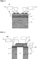
FIG. 1 is a view showing an example of a cross-sectional structure of a laminated substrate according to an embodiment of the present disclosure. -
FIG. 2 is a view showing a modified example of the cross-sectional structure of the laminated substrate according to an embodiment of the present disclosure. -
FIG. 3 is a schematic constitution view of a piezoelectric film device according to an embodiment of the present disclosure. -
FIG. 4 is a view showing a modified example of the cross-sectional structure of the piezoelectric film device according to an embodiment of the present disclosure. -
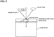
FIG. 5 is a view showing a measurement principle of a sound speed of a piezoelectric film according to an embodiment of the present disclosure. - An embodiment of the present disclosure will be described hereafter, with reference to drawings.
- As shown in
FIG. 1 , a laminatedsubstrate 10 according to the present embodiment is constituted as a laminate including asubstrate 1, a base film 7 provided on thesubstrate 1, a piezoelectric film (piezoelectric thin film) 3 provided on the base film 7, and atop electrode film 4 provided on thepiezoelectric film 3. - As the
substrate 1, a single-crystal silicon (Si)substrate 1a on which a surface oxide film (SiO2-film) 1b such as a thermal oxide film or a CVD (Chemical Vapor Deposition) oxide film is provided (formed), namely, a Si-substrate having the surface oxide film, can be used preferably. Further, as shown inFIG. 2 , a Si-substrate 1a having aninsulating film 1d provided on its surface may also be used as thesubstrate 1, theinsulating film 1d containing an insulating material other than SiO2. Further, a Si-substrate 1a in which Si-(100) plane or Si-(111) plane, etc., is exposed on a surface thereof, namely, a Si-substrate not having thesurface oxide film 1b or theinsulating film 1d may also be used as thesubstrate 1. Further, an SOI (Silicon On Insulator) substrate, a quartz glass (SiO2) substrate, a gallium arsenide (GaAs) substrate, a sapphire (Al2O3) substrate, a metal substrate containing a metal material such as stainless steel may also be used as thesubstrate 1. The single-crystal Si-substrate 1a has a thickness of 300 to 1000 µm for example, and thesurface oxide film 1b has a thickness of 5 to 3000 nm for example. - The base film 7 can be formed (provided, deposited) using platinum (Pt) for example. The base film 7 is a single-crystal film or a poly-crystal film (they are also referred to as Pt-film hereafter). Preferably, crystals constituting the Pt-film are preferentially oriented in (111) plane direction with respect to a surface of the
substrate 1. Namely, it is preferable that a surface of the Pt-film (a surface which is a base of the piezoelectric film 3) is mainly constituted of Pt-(111) plane. The Pt-film can be formed using a method such as a sputtering method, or an evaporation method. In addition to Pt, the base film 7 may also be formed using various metals such as gold (Au), ruthenium (Ru), or iridium (Ir), an alloy mainly composed of the above various metals, or a metallic oxide such as strontium ruthenate (SrRuO3) or lanthanum nickel oxide (LaNiO3), etc. Anadhesion layer 6 mainly composed of titanium (Ti), tantalum (Ta), titanium oxide (TiO2), or nickel (Ni), etc., for example is formed between thesubstrate 1 and the base film 7 in order to enhance an adhesion between them. Theadhesion layer 6 can be formed using a method such as a sputtering method, or an evaporation method. The base film 7 has a thickness of 100 to 400 nm for example, and theadhesion layer 6 has a thickness of 1 to 200 nm for example. - The
piezoelectric film 3 can be formed (provided, deposited) using alkali niobium oxide which contains for example, potassium (K), sodium (Na), and niobium (Nb), and which is represented by a composition formula of (K1-xNax)NbO3. Namely, thepiezoelectric film 3 can be formed using potassium sodium niobate (KNN). A coefficient x [= Na/(K+Na)] in the above composition formula is a value in a range of 0<x<1, preferably 0.4≤x≤0.7. Thepiezoelectric film 3 is a poly-crystal film of KNN (also referred to as KNN-film 3 hereafter). A crystal structure of KNN is a perovskite structure. - Preferably, crystals constituting the KNN-
film 3 are preferentially oriented in (001) plane direction with respect to the surface of thesubstrate 1. Namely, it is preferable that a surface of the KNN-film 3 (a surface which is a base of the top electrode film 4) is mainly constituted of KNN-(001) plane. By forming the KNN-film 3 directly on the Pt-film (base film 7) preferentially oriented in (111) plane direction with respect to the surface of thesubstrate 1, crystals constituting the KNN-film 3 can be easily preferentially oriented in (001) plane direction with respect to the surface of thesubstrate 1. For example, 85 % or more of crystals of a crystal group constituting the KNN-film 3 can be oriented in (001) plane direction with respect to the surface of thesubstrate 1, and thereby a region of 85% or more of the surface of the KNN-film 3 can be KNN-(001) plane. Namely, a (001)-orientation ratio of the KNN-film 3 can be 85 % or more. - The KNN-
film 3 can be formed using a method such as a sputtering method, a PLD (Pulsed Laser Deposition) method, or a sol-gel method. A composition ratio of the KNN-film 3 can be adjusted by controlling a composition of a target material used during sputtering, for example. The target material can be produced by mixing and firing K2CO3-powder, Na2CO3-powder, Nb2O5-powder, etc., for example. In this case, the composition of the target material can be controlled by adjusting a mixed ratio of K2CO3-powder, Na2CO3-powder, Nb2O5-powder, etc. - In the KNN-
film 3, its sound speed is 5100 m/s or more, preferably 5700 m/s or more, and more preferably 5800 m/s or more. - In this specification, the sound speed is measured using Brillouin Oscillation method.
Fig. 5 shows an example of a measurement principle view of the sound speed by Brillouin Oscillation method. As exemplified inFIG. 5 , first, the surface of the KNN-film 3 is irradiated with a pump light and a probe light which are femtosecond laser pulsed light for example. The pump light is the light for exciting a sound wave in the KNN-film 3. Specifically, the surface of the KNN-film 3 is irradiated with the pump light vertically to the surface of the KNN-film 3, to thereby increase locally and instantaneously a temperature in the vicinity of the surface of the KNN-film 3 at an irradiation position of the pump light. The sound wave (ultrasonic pulse) is excited in the KNN-film 3, due to a thermal stress generated at the above position. This sound wave is a longitudinal wave which mainly propagates in a vertical direction to the surface of the KNN-film 3. A part of the sound wave which propagates in the KNN-film 3 toward the base film 7, is reflected at an interface between the KNN-film 3 and the base film 7, and returns to the surface (vicinity of the surface) of the KNN-film 3. As a result, the surface of the KNN-film 3 is deformed. The probe light is the light for irradiating the irradiation position of the pump light on the surface of the KNN-film 3 at a prescribed angle with respect to the surface of the KNN-film 3. A prescribed delay time may be given to the probe light. The reflected light of the probe light is continuously detected by a detector, and its reflectance is continuously measured, to thereby obtain a function of a delay time between the pump light and the probe light, and the reflectance of the probe light. When the surface of the KNN-film 3 is deformed by the reflected light of the pump light as described above, the reflectance of the reflected light of the probe light is varied, and a peak (echo) occurs. As a result, the time from the irradiation of the pump light to the occurrence of the peak, coincides with a propagation time of the sound wave which propagates in the KNN-film 3 and returns to the surface of the KNN-film 3. In this embodiment, since a thickness of the KNN-film 3 is already known, the sound speed of the KNN-film 3 can be calculated based on the time between the peaks. - The sound speed of the KNN-
film 3 depends on an orientation state in (001) plane direction of the crystals constituting the KNN-film 3 (also referred to as (001)-orientation state of the KNN-film 3 hereafter). The sound speed of the KNN-film 3 increases as the number of crystals oriented in (001) plane direction in the KNN-film 3 increase, namely as the (001)-orientation ratio of the KNN-film 3 becomes higher. Further, the sound speed of the KNN-film 3 decreases as the number of the crystals oriented in (001) plane direction in the KNN-film 3 decrease, namely as the (001)-orientation ratio of the KNN-film 3 becomes lower. Hereafter, high (001)-orientation ratio of the KNN-film 3 is also called "(001)-high orientation", and low (001)-orientation ratio of the KNN-film 3 is also called "(001)-low orientation". - For example, a mixed gas (Ar/O2-mixed gas) of argon (Ar) gas and oxygen (O2) gas is used as an atmosphere gas during sputtering of the KNN-
film 3. However, water existing in a chamber is sometimes mixed in the atmosphere gas although its content is very small. The (001)-orientation state of the KNN-film 3 greatly depends on a partial pressure of H2O contained in the atmosphere gas during sputtering. The (001)-orientation state tends to be (001)-high orientation when H2O-partial pressure is low, and tends to be (001)-low orientation when H2O-partial pressure is high. The (001)-orientation ratio of the KNN-film 3 can be adjusted by controlling the partial pressure of H2O containing in the Ar/O2-mixed gas during sputtering. The (001)-orientation ratio of the KNN-film 3 can be 85 % or more by adjusting the H2O-partial pressure to 1/100 or less, preferably 1/300 or less of a pressure in a growth atmosphere, for example. - When a later-described
piezoelectric film device 30 produced by processing thelaminated substrate 10, functions as a filter device of a high frequency band, the sound speed of the KNN-film 3 is preferably fast. However, according to a current state of the art, the sound speed of the KNN-film 3 is 6000 m/s or less for example, due to an upper limit of the (001)-orientation ratio of the KNN-film 3, or a mixture of inevitable impurities into the KNN-film 3 during formation of the KNN-film 3, etc. - An absolute value |d31| of a piezoelectric constant of the KNN-
film 3 is 90 pm/V or more for example (|d31|≥90 pm/V), preferably 100 pm/V or more (|d31|≥100 pm/V). A thickness of the KNN-film 3 is 0.5 to 5 µm or less for example. - The KNN-
film 3 may contain an element such as copper (Cu), manganese (Mn), lithium (Li), Ta, antimony (Sb) other than K, Na, Nb in a range of 5 at% or less. - The
top electrode film 4 can be formed (provided, deposited) using various metals such as Pt, Au, aluminum (Al), or Cu, or an alloy of these various metals, for example. Thetop electrode film 4 can be formed using a method such as a sputtering method, an evaporation method, a plating method, or a metal paste method. Thetop electrode film 4 does not greatly affect the crystal structure of the KNN-film 3 unlike the base film 7. Therefore, a material and a crystal structure of thetop electrode film 4, and a method for forming thetop electrode film 4 are not particularly limited. An adhesion layer mainly composed of Ti, Ta, TiO2, Ni, etc., for example may be formed between the KNN-film 3 and thetop electrode film 4 in order to enhance an adhesion between them. Thetop electrode film 4 has a thickness of 100 to 5000 nm for example, and the adhesion layer has a thickness of 1 to 200 nm in a case of forming the adhesion layer. -
FIG. 3 shows a schematic constitution view of adevice 30 having the piezoelectric film of the present embodiment (also referred to aspiezoelectric film device 30 hereafter). Thepiezoelectric film device 30 is constituted including at least anelement 20 having the piezoelectric film (also referred to aspiezoelectric film element 20 hereafter) obtained by forming the abovelaminated substrate 10 into a prescribed shape, and a voltage application means 11a and a voltage detection means 11b which are connected to thepiezoelectric film element 20. - The
piezoelectric film element 20 has pattern electrodes obtained by forming thetop electrode film 4 into a prescribed pattern. Thepiezoelectric film element 20 has a pair of positive-negative pattern electrodes 4pi which are input-side electrodes, and a pair of positive-negative pattern electrodes 4p2 which are output-side electrodes. A comb-shaped electrode (IDT: Inter Digital Transducer) is used as the pattern electrodes 4pi and 4p2, for example. - By connecting the voltage application means 11a between the pattern electrodes 4p1 and connecting the voltage detection means 11b between the pattern electrodes 4p2, the
piezoelectric film device 30 can function as a filter device such as a SAW filter. By applying a voltage between the pattern electrodes 4pi using the voltage application means 11a, SAW can excite on the surface of the KNN-film 3. A frequency of excited SAW can be adjusted by adjusting a pitch between the pattern electrodes 4p1, for example. For example, the frequency of SAW becomes high as a pitch of IDT as the pattern electrodes 4pi is short, and the frequency of SAW becomes low as the above pitch is long. A voltage is generated between the pattern electrodes 4p2, due to SAW having a prescribed frequency (frequency component) determined according to the pitch of IDT as the pattern electrodes 4p2 in the SAW which is excited by the voltage application means 11a, propagates in the KNN-film 3, and reaches the pattern electrodes 4p2. By detecting this voltage using the voltage detection means 11b, SAW having a prescribed frequency in the excited SAW can be extracted. The "prescribed frequency" as used here can include not only a prescribed frequency but also a prescribed frequency band in which a center frequency is prescribed frequency. - Next, a method for manufacturing the above
laminated substrate 10 will be described. First, the base film 7 is formed on any one of main surfaces of thesubstrate 1. It is also acceptable to prepare thesubstrate 1 on which the base film 7 is formed in advance on any one of its main surfaces. Next, the KNN-film 3 is formed on the base film 7 using the sputtering method for example. Thereafter, thetop electrode film 4 is formed on the KNN-film 3 using the sputtering method for example, and therefore thelaminated substrate 10 is obtained. Then, thelaminated substrate 10 is formed into a prescribed shape, for example, thetop electrode film 4 is formed into the pattern electrodes 4p1 and 4p2 by etching, etc., and therefore thepiezoelectric film element 20 is obtained. Further, the voltage application means 11a is connected between the pattern electrodes 4p1 of thepiezoelectric film element 20, and the voltage detection means 11b is connected between the pattern electrodes 4p2 of thepiezoelectric film element 20, and therefore thepiezoelectric film device 30 is obtained. - According to the present embodiment, one or more of the following effects can be obtained.
- (a) Since the sound speed of the KNN-
film 3 is 5100 m/s or more, a resonance frequency of thepiezoelectric film device 30 produced by processing thelaminated substrate 10 having the KNN-film 3 can be high frequency. Thereby, thepiezoelectric film device 30 can be suitably applied to a filter device of a high frequency band compared to a piezoelectric film device obtained by processing a laminated substrate having conventional KNN-film. Namely, since the sound speed of the KNN-film 3 is fast, thepiezoelectric film device 30 can suitably function as a high frequency filter.
When the sound speed of the KNN-film 3 is less than 5100 m/s, it is difficult to use the piezoelectric film device as the high frequency filter, in some cases. Further, even in a case that such a piezoelectric film device can be used as the high frequency filter, a filter property of this high frequency filter becomes low, in some cases. - (b) Since the sound speed of the KNN-
film 3 is 5100 m/s or more, thepiezoelectric film device 30 can be actuated at a higher frequency without shortening the pitch of the pattern electrodes 4p, when the thickness of the KNN-film 3 is constant. Namely, when thepiezoelectric film device 30 capable of actuating at high frequency is produced, it is not necessary to make a minute pattern electrodes 4p. - (c) Since the (001)-orientation ratio of the KNN-
film 3 is 85% or more, the sound speed of the KNN-film 3 can be 5700 m/s or more. Further, the (001)-orientation ratio of the KNN-film 3 is 90 % or more, the sound speed of the KNN-film 3 can be 5800 m/s or more. It is already found by the present inventors that the sound speed of the KNN-film 3 is 5650 m/s when the (001)-orientation ratio of the KNN-film 3 is 78 %, and the sound speed of the KNN-film 3 is 5820 m/s for example when the (001)-orientation ratio of the KNN-film 3 is 92 %. - (d) Since the absolute value |d31| of the piezoelectric constant of the KNN-
film 3 is 90pm/V or more, the high frequency filter can be a low loss filter, or a reduction of a detecting sensitivity of frequency can be prevented, when thepiezoelectric film device 30 is used as the high frequency filter. Namely, since the KNN-film 3 has excellent piezoelectric property, a performance of thepiezoelectric film device 30 can be enhanced. - Here, for reference, conventional laminated substrate using for the high frequency filter will be described.
- Conventionally, for example, a piezoelectric film device using a laminated substrate having a piezoelectric film made of aluminum nitride (AlN) (also referred to as AIN-film hereafter), functions as the high frequency filter. However, there is a problem as follows: although a sound speed of the AIN-film is faster than that of the KNN-film, an absolute value |d31| of a piezoelectric constant of the AIN-film is smaller than that of the KNN-film. For example, although the sound speed of the AIN-film is 10000 m/s or more, the absolute value |d31| of the piezoelectric constant of the AIN-film is about 5 pm/V. Therefore, when this piezoelectric film device functions as the high frequency filter, this filter becomes low performance filter.
- Further, for example, it is also conceivable that a piezoelectric film device using a laminated substrate having a piezoelectric film made of lead zirconate titanate (PZT) (also referred to as PZT-film hereafter), functions as the high frequency filter. However, there is a problem as follows: although the PZT-film has the piezoelectric property similar to that of the KNN-film, a sound speed of the PZT-film is slower than that of the KNN-film. For example, although an absolute value |d31| of a piezoelectric constant of the PZT-film is 90 pm/V or more, the sound speed of the PZT-film is about 4000 to 5000 m/s. Therefore, it is necessary to make a minute pitch between the pattern electrodes compared to the pitch of the piezoelectric film device having the above KNN-film, in order to function the piezoelectric film device having the PZT-film as the high frequency filter. There is also a problem as follows: since the pitch of the pattern electrodes in the high frequency filter is micrometer (µm) order, in the piezoelectric film device having the PZT-film, it is very difficult to make a minute pitch between the pattern electrodes with high accuracy.
- The present embodiment is not limited to the abovementioned embodiment, and can be modified as the following modified examples.
- The above
piezoelectric film device 30 may be applied to a filter device utilizing a bulk acoustic wave. For example, thepiezoelectric film device 30 may function as a Bulk Acoustic Wave (BAW) filter such as a piezoelectric thin film acoustic resonator (FBAR: Film Bulk Acoustic Resonator).FIG.4 shows a schematic constitution view of apiezoelectric film device 30A capable of functioning as a FBAR filter. As shown inFIG. 4 , thepiezoelectric film device 30A is constituted including at least apiezoelectric film element 20A obtained by forming alaminated substrate 10A into a prescribed shape, and the voltage application means 11a and the voltage detection means 11b which are connected to thepiezoelectric film element 20A. - The
laminated substrate 10A is constituted as a laminate including thesubstrate 1, thebottom electrode film 2 provided on thesubstrate 1, the KNN-film (piezoelectric film) 3 provided on thebottom electrode film 2, and thetop electrode film 4 provided on the KNN-film 3. Thebottom electrode film 2 can be the same constitution as the above base film 7. The KNN-film 3 has a region where the thickness is thin (also referred to as thin area hereafter). Further, thelaminated substrate 10A has acavity 8 for oscillating freely the KNN-film 3. In this modified example, thecavity 8 is formed by forming a through hole on thesubstrate 1. Thecavity 8 may be formed after forming the KNN-film 3 and before forming thetop electrode film 4, or may be formed after forming thetop electrode film 4. Thecavity 8 is not limited to the constitution exemplified inFIG. 4 , and may be publicly-known various constitutions. Further, in thepiezoelectric film element 20A, thetop electrode film 4 is not required to be IDT, and thetop electrode film 4 may be formed into a prescribed shape (pattern). - In the
piezoelectric film device 30A, the voltage application means 11a and the voltage detection means 11b are connected between thebottom electrode film 2 and thetop electrode film 4, respectively. In this modified example, the voltage application means 11a is connected to thetop electrode film 4 located on an area other than the thin area of the KNN-film 3, and the voltage detection means 11b is connected to thetop electrode film 4 located on the thin area of the KNN-film 3. - By applying a voltage between the
bottom electrode film 2 and thetop electrode film 4 using the voltage application means 11a, BAW is excited in the KNN-film 3. A frequency of BAW, namely, a resonance frequency of the KNN-film 3 can be adjusted by adjusting a thickness of the region other than the thin area of the KNN-film 3, for example. The resonance frequency of the KNN-film 3 (BAW) becomes high as the thickness of the KNN-film 3 becomes thin, and the resonance frequency of the KNN-film 3 becomes low as the thickness of the KNN-film 3 becomes thick. A voltage is generated between thebottom electrode film 2 and thetop electrode film 4, due to BAW having a prescribed frequency (frequency component) determined according to the thickness of the thin region of the KNN-film 3, etc., in the BAW which is excited by the voltage application means 11a, propagates in the KNN-film 3, and reaches an out-put side electrode. By detecting this voltage using the voltage detection means 11b, BAW having a prescribed frequency in the excited BAW can be extracted. - In this modified example as well, the similar effect as the above embodiment can be obtained. Further, in this modified example, namely, in BAW filter, since it is not necessary to form the
top electrode film 4 into IDT, a minute processing of thetop electrode film 4 is not required. Further, since BAW filter does not have IDT, it is easy to produce a filter with lower loss and higher electric power resistance than SAW filter. - As described above, explanation has been given specifically for the embodiments of the present disclosure. However, the present disclosure is not limited thereto, and can be variously modified in a range not departing from the gist of the disclosure.
- For example, the piezoelectric film device according to the above embodiment can function as an actuator by connecting the voltage application means between the bottom electrode film (base film) and the top electrode film. By applying a voltage between the bottom electrode film and the top electrode film using the voltage application means, the KNN-film (piezoelectric film) can be deformed. Various members connected to the piezoelectric film device can be actuated due to the above deformation motion. In this case, the piezoelectric film device can be applied to a head for an inkjet printer, a MEMS mirror for a scanner, and a vibrator for an ultrasonic generator, etc., for example.
- Further, for example, the piezoelectric film device according to the above embodiment can function as a sensor by connecting the voltage detection means between the bottom electrode film (base film) and the top electrode film. When the KNN-film is deformed according to a variation of some physical quantity, a voltage is generated between the bottom electrode film and the top electrode film due to the deformation. By detecting this voltage using the voltage detection means, the physical quantity applied to the KNN-film can be measured. In this case, the piezoelectric film device can be applied to an angular velocity sensor, an ultrasonic sensor, a pressure sensor, and an acceleration sensor, etc., for example.
- Further, in the above embodiment, the substrate may be removed from the laminated substrate when forming the laminated substrate into the piezoelectric film element, as long as the piezoelectric film device produced using the laminated substrate (piezoelectric film element) is applied to desired applications such as a high frequency filter.
- Preferable aspects of the present disclosure will be supplementarily described hereafter.
- According to an aspect of the present disclosure, there is provided a laminated substrate having a piezoelectric film, including:
- a substrate; and
- a piezoelectric film provided on the substrate interposing a base film,
- wherein the piezoelectric film has an alkali niobium oxide based perovskite structure represented by a composition formula of (K1-xNax)NbO3 (0<x<1) and preferentially oriented in (001) plane direction, and
- a sound speed of the piezoelectric film is 5100 m/s or more.
- Preferably, there is provided the substrate of the
supplementary description 1, wherein an absolute value |d31| of a piezoelectric constant of the piezoelectric film is 90 pm/V or more. - According to another aspect of the present disclosure, there is provided a laminated substrate having a piezoelectric film, including:
- a substrate; and
- a piezoelectric film on the substrate interposing a base film,
- wherein a sound speed of the piezoelectric film is 5100 m/s or more, and an absolute value |d31| of a piezoelectric constant of the piezoelectric film is 90pm/V or more.
- Preferably, there is provided the substrate of the
supplementary description 3, wherein the piezoelectric film has an alkali niobium oxide based perovskite structure represented by a composition formula of (K1-xNax)NbO3 (0<x<1) and preferentially oriented in (001) plane direction. - Preferably, there is provided the substrate of any one of the
supplementary descriptions 1 to 4, wherein the sound speed of the piezoelectric film is 5700 m/s or more. - Preferably, there is provided the substrate of any one of the
supplementary descriptions 1 to 5, wherein the piezoelectric film comprises crystals (alkali niobium oxide) constituting the piezoelectric film, and 85% or more of the crystals are oriented in (001) plane direction. - Preferably, there is provided the substrate of any one of the
supplementary descriptions 1 to 6, wherein a thickness of the piezoelectric film is 0.5 µm or more and 5 µm or less. - According to further another aspect of the present disclosure, there is provided an element having a piezoelectric film or a device having a piezoelectric film, including:
- a substrate;
- a piezoelectric film provided on the substrate interposing a base film; and
- an electrode film (pattern electrode film) provided on the piezoelectric film,
- wherein the piezoelectric film has an alkali niobium oxide based perovskite structure represented by a composition formula of (K1-xNax)NbO3 (0<x<1) and preferentially oriented in (001) plane direction, and
- a sound speed of the piezoelectric film is 5100 m/s or more.
- According to further another aspect of the present disclosure, there is provided an element having a piezoelectric film or a device having a piezoelectric film, including:
- a substrate;
- a piezoelectric film provided on the substrate interposing a base film; and
- an electrode film (pattern electrode film) provided on the piezoelectric film,
- wherein a sound speed of the piezoelectric film is 5100 m/s or more, and an absolute value |d31| of a piezoelectric constant of the piezoelectric film is 90 pm/V or more.
- According to further another aspect of the present disclosure, there is provided an element having a piezoelectric film or a device having a piezoelectric film, including:
- a substrate;
- a bottom electrode film provided on the substrate;
- a piezoelectric film provided on the bottom electrode film; and
- a top electrode film provided on the piezoelectric film,
- wherein the piezoelectric film has an alkali niobium oxide based perovskite structure represented by a composition formula of (K1-xNax)NbO3 (0<x<1) and preferentially oriented in (001) plane direction, and
- a sound speed of the piezoelectric film is 5100 m/s or more.
- According to further another aspect of the present disclosure, there is provided an element having a piezoelectric film or a device having a piezoelectric film, including:
- a substrate;
- a bottom electrode film provided on the substrate;
- a piezoelectric film provided on the bottom electrode film; and
- a top electrode film provided on the piezoelectric film,
- wherein a sound speed of the piezoelectric film is 5100 m/s or more, and an absolute value |d31| of a piezoelectric constant of the piezoelectric film is 90 pm/V or more.
- According to further another aspect of the present disclosure, there is provided a method for manufacturing a laminated substrate having a piezoelectric film, including:
forming a piezoelectric film on a substrate interposing a base film, the piezoelectric film having an alkali niobium oxide based perovskite structure represented by a composition formula of (K1-xNax)NbO3 (0<x<1) and preferentially oriented in (001) plane direction, and having a sound speed of 5100 m/s or more. - According to further another aspect of the present disclosure, there is provided a method for manufacturing a laminated substrate having a piezoelectric film, including:
forming a piezoelectric film on a substrate interposing a base film, with its sound speed being 5100 m/s or more and its absolute value |d31| of a piezoelectric constant being 90 pm/V or more. -
- 1
- Substrate
- 3
- Piezoelectric film
- 10
- Laminated substrate
Claims (6)
- A laminated substrate having a piezoelectric film, comprising:a substrate; anda piezoelectric film provided on the substrate interposing a base film,wherein the piezoelectric film has an alkali niobium oxide based perovskite structure represented by a composition formula of (K1-xNax)NbO3 (0<x<1) and preferentially oriented in (001) plane direction, anda sound speed of the piezoelectric film is 5100 m/s or more.
- A laminated substrate having a piezoelectric film, comprising:a substrate; anda piezoelectric film on the substrate interposing a base film,wherein a sound speed of the piezoelectric film is 5100 m/s or more, and an absolute value |d31| of a piezoelectric constant of the piezoelectric film is 90pm/V or more.
- An element having a piezoelectric film, comprising:a substrate;a piezoelectric film provided on the substrate interposing a base film; andan electrode film provided on the piezoelectric film,wherein the piezoelectric film has an alkali niobium oxide based perovskite structure represented by a composition formula of (K1-xNax)NbO3 (0<x<1) and preferentially oriented in (001) plane direction, anda sound speed of the piezoelectric film is 5100 m/s or more.
- An element having a piezoelectric film, comprising:a substrate;a piezoelectric film provided on the substrate interposing a base film; andan electrode film provided on the piezoelectric film,wherein a sound speed of the piezoelectric film is 5100 m/s or more, and an absolute value |d31| of a piezoelectric constant of the piezoelectric film is 90 pm/V or more.
- A method for manufacturing a laminated substrate having a piezoelectric film, comprising:
forming a piezoelectric film on a substrate interposing a base film, the piezoelectric film having an alkali niobium oxide based perovskite structure represented by a composition formula of (K1-xNax)NbO3 (0<x<1) and preferentially oriented in (001) plane direction, and having a sound speed of 5100 m/s or more. - A method for manufacturing a laminated substrate having a piezoelectric film, comprising:
forming a piezoelectric film on a substrate interposing a base film, with its sound speed being 5100 m/s or more and its absolute value |d31| of a piezoelectric constant being 90 pm/V or more.
Applications Claiming Priority (2)
| Application Number | Priority Date | Filing Date | Title |
|---|---|---|---|
| JP2017136447A JP2019021994A (en) | 2017-07-12 | 2017-07-12 | Multilayer substrate having piezoelectric film, element having piezoelectric film, and method of manufacturing multilayer substrate having piezoelectric film |
| PCT/JP2018/023864 WO2019012960A1 (en) | 2017-07-12 | 2018-06-22 | Laminated substrate provided with piezoelectric film, element provided with piezoelectric film, and method for producing laminated substrate provided with piezoelectric film |
Publications (2)
| Publication Number | Publication Date |
|---|---|
| EP3654528A1 true EP3654528A1 (en) | 2020-05-20 |
| EP3654528A4 EP3654528A4 (en) | 2021-06-02 |
Family
ID=65001901
Family Applications (1)
| Application Number | Title | Priority Date | Filing Date |
|---|---|---|---|
| EP18832152.5A Pending EP3654528A4 (en) | 2017-07-12 | 2018-06-22 | LAMINATED SUBSTRATE PROVIDED WITH A PIEZOELECTRIC FILM, ELEMENT PROVIDED WITH A PIEZOELECTRIC FILM, AND PROCESS FOR THE PRODUCTION OF A LAMINATED SUBSTRATE WITH A PIEZOELECTRIC FILM |
Country Status (4)
| Country | Link |
|---|---|
| US (2) | US11557713B2 (en) |
| EP (1) | EP3654528A4 (en) |
| JP (1) | JP2019021994A (en) |
| WO (1) | WO2019012960A1 (en) |
Families Citing this family (4)
| Publication number | Priority date | Publication date | Assignee | Title |
|---|---|---|---|---|
| JP2019021994A (en) * | 2017-07-12 | 2019-02-07 | 株式会社サイオクス | Multilayer substrate having piezoelectric film, element having piezoelectric film, and method of manufacturing multilayer substrate having piezoelectric film |
| JP7352347B2 (en) * | 2018-12-07 | 2023-09-28 | 住友化学株式会社 | Piezoelectric laminate, piezoelectric element, and piezoelectric laminate manufacturing method |
| US20230270013A1 (en) * | 2020-06-30 | 2023-08-24 | Sumitomo Chemical Company, Limited | Piezoelectric stack, piezoelectric element, and method of manufacturing piezoelectric stack |
| CN116601871A (en) * | 2020-10-06 | 2023-08-15 | 株式会社村田制作所 | Elastic wave device |
Family Cites Families (23)
| Publication number | Priority date | Publication date | Assignee | Title |
|---|---|---|---|---|
| US6312568B2 (en) * | 1999-12-07 | 2001-11-06 | Applied Materials, Inc. | Two-step AIN-PVD for improved film properties |
| US6953977B2 (en) * | 2000-02-08 | 2005-10-11 | Boston Microsystems, Inc. | Micromechanical piezoelectric device |
| JP4345329B2 (en) * | 2003-03-13 | 2009-10-14 | セイコーエプソン株式会社 | Surface acoustic wave device |
| JP4192648B2 (en) * | 2003-03-26 | 2008-12-10 | セイコーエプソン株式会社 | Method for producing potassium niobate single crystal thin film and method for producing surface acoustic wave device |
| JP2005057707A (en) * | 2003-08-07 | 2005-03-03 | Sony Corp | Thin film bulk acoustic resonator and microelectromechanical system devices |
| JP5044902B2 (en) * | 2005-08-01 | 2012-10-10 | 日立電線株式会社 | Piezoelectric thin film element |
| JP4735840B2 (en) | 2005-12-06 | 2011-07-27 | セイコーエプソン株式会社 | Piezoelectric laminate, surface acoustic wave device, thin film piezoelectric resonator, and piezoelectric actuator |
| JP4396860B2 (en) * | 2006-05-26 | 2010-01-13 | セイコーエプソン株式会社 | Method for manufacturing piezoelectric layer |
| JP2008159807A (en) | 2006-12-22 | 2008-07-10 | Hitachi Cable Ltd | Piezoelectric thin film element and actuator and sensor manufactured using the piezoelectric thin film element |
| JP5446146B2 (en) * | 2008-07-01 | 2014-03-19 | 日立金属株式会社 | Piezoelectric thin film element, sensor and actuator |
| JP2010068503A (en) * | 2008-08-13 | 2010-03-25 | Seiko Epson Corp | Surface acoustic wave element |
| JP5515675B2 (en) * | 2009-11-20 | 2014-06-11 | 日立金属株式会社 | Piezoelectric thin film element and piezoelectric thin film device |
| WO2011121863A1 (en) * | 2010-03-29 | 2011-10-06 | 日立電線株式会社 | Piezoelectric thin-film element, process for producing same, and piezoelectric thin-film device |
| JP5056914B2 (en) | 2010-07-07 | 2012-10-24 | 日立電線株式会社 | Piezoelectric thin film element and piezoelectric thin film device |
| CN104334498B (en) * | 2012-04-16 | 2016-12-21 | 佳能株式会社 | Sodium niobate powder and its preparation method, ceramic preparation method and piezoelectric element |
| WO2013191122A1 (en) * | 2012-06-22 | 2013-12-27 | 株式会社村田製作所 | Elastic wave device |
| CN103703793B (en) * | 2012-06-26 | 2015-02-18 | 本多电子株式会社 | Electromechanical conversion element and manufacturing method therefor |
| JP5858385B2 (en) * | 2012-08-07 | 2016-02-10 | 住友化学株式会社 | Piezoelectric element, piezoelectric device and manufacturing method thereof |
| JP6179669B2 (en) * | 2014-05-19 | 2017-08-16 | 株式会社村田製作所 | Piezoelectric thin film and piezoelectric thin film element |
| JP6605215B2 (en) | 2015-03-26 | 2019-11-13 | 住友化学株式会社 | Ferroelectric thin film multilayer substrate, ferroelectric thin film element, and method for manufacturing ferroelectric thin film multilayer substrate |
| JP6239566B2 (en) * | 2015-10-16 | 2017-11-29 | 株式会社サイオクス | Multilayer substrate with piezoelectric thin film, piezoelectric thin film element, and manufacturing method thereof |
| JP6790749B2 (en) * | 2016-11-16 | 2020-11-25 | セイコーエプソン株式会社 | Piezoelectric elements and piezoelectric element application devices |
| JP2019021994A (en) * | 2017-07-12 | 2019-02-07 | 株式会社サイオクス | Multilayer substrate having piezoelectric film, element having piezoelectric film, and method of manufacturing multilayer substrate having piezoelectric film |
-
2017
- 2017-07-12 JP JP2017136447A patent/JP2019021994A/en active Pending
-
2018
- 2018-06-22 US US16/628,524 patent/US11557713B2/en active Active
- 2018-06-22 WO PCT/JP2018/023864 patent/WO2019012960A1/en not_active Ceased
- 2018-06-22 EP EP18832152.5A patent/EP3654528A4/en active Pending
-
2022
- 2022-12-15 US US18/082,531 patent/US20230115136A1/en not_active Abandoned
Also Published As
| Publication number | Publication date |
|---|---|
| JP2019021994A (en) | 2019-02-07 |
| US20230115136A1 (en) | 2023-04-13 |
| WO2019012960A1 (en) | 2019-01-17 |
| US20200161533A1 (en) | 2020-05-21 |
| US11557713B2 (en) | 2023-01-17 |
| EP3654528A4 (en) | 2021-06-02 |
Similar Documents
| Publication | Publication Date | Title |
|---|---|---|
| US20230115136A1 (en) | Laminated substrate having piezoelectric film, element having piezoelectric film and method for manufacturing this laminated substrate | |
| US12527226B2 (en) | Laminated substrate with piezoelectric thin film, piezoelectric thin film element and method for manufacturing this element | |
| JP5433367B2 (en) | Lamb wave device | |
| EP4135344B1 (en) | Production method for piezoelectric laminate | |
| EP3637486B1 (en) | Laminated substrate with potassium sodium niobate piezoelectric film and manufacturing method thereof | |
| EP3540797B1 (en) | Piezoelectric laminate, method of manufacturing piezoelectric laminate, and piezoelectric element | |
| JP2010220204A (en) | Lamb wave device | |
| EP3901097A1 (en) | Piezoelectric laminate, piezoelectric element, and piezoelectric laminate manufacturing method | |
| EP3540800B1 (en) | Piezoelectric laminate, method of manufacturing the piezoelectric laminate and piezoelectric device | |
| JP6934746B2 (en) | A method for manufacturing a laminated substrate having a piezoelectric film, an element having a piezoelectric film, and a laminated substrate having a piezoelectric film. | |
| EP3761383A1 (en) | Piezoelectric laminate, piezoelectric element and method of manufacturing the piezoelectric laminate | |
| JP7037892B2 (en) | A method for manufacturing a laminated substrate having a piezoelectric film, a method for manufacturing an element having a piezoelectric film, and a laminated body having a piezoelectric film. | |
| EP3772115B1 (en) | Piezoelectric element and manufacturing method thereof | |
| JP7320098B2 (en) | Piezoelectric laminate, method for manufacturing piezoelectric laminate, and piezoelectric device | |
| EP3772116B1 (en) | Piezoelectric element and manufacturing method thereof | |
| JP6961770B2 (en) | Laminated substrate with piezoelectric thin film and piezoelectric thin film element | |
| JP2019117943A (en) | Piezoelectric thin film-attached laminate board and piezoelectric thin film element |
Legal Events
| Date | Code | Title | Description |
|---|---|---|---|
| STAA | Information on the status of an ep patent application or granted ep patent |
Free format text: STATUS: THE INTERNATIONAL PUBLICATION HAS BEEN MADE |
|
| PUAI | Public reference made under article 153(3) epc to a published international application that has entered the european phase |
Free format text: ORIGINAL CODE: 0009012 |
|
| STAA | Information on the status of an ep patent application or granted ep patent |
Free format text: STATUS: REQUEST FOR EXAMINATION WAS MADE |
|
| 17P | Request for examination filed |
Effective date: 20200110 |
|
| AK | Designated contracting states |
Kind code of ref document: A1 Designated state(s): AL AT BE BG CH CY CZ DE DK EE ES FI FR GB GR HR HU IE IS IT LI LT LU LV MC MK MT NL NO PL PT RO RS SE SI SK SM TR |
|
| AX | Request for extension of the european patent |
Extension state: BA ME |
|
| DAV | Request for validation of the european patent (deleted) | ||
| DAX | Request for extension of the european patent (deleted) | ||
| RIC1 | Information provided on ipc code assigned before grant |
Ipc: H01L 41/09 20060101ALN20201215BHEP Ipc: H03H 9/02 20060101ALI20201215BHEP Ipc: H01L 41/187 20060101ALN20201215BHEP Ipc: H01L 41/08 20060101ALN20201215BHEP Ipc: H01L 41/316 20130101ALN20201215BHEP Ipc: H03H 9/25 20060101AFI20201215BHEP Ipc: H01L 41/113 20060101ALN20201215BHEP Ipc: H03H 3/02 20060101ALN20201215BHEP Ipc: H03H 3/08 20060101ALI20201215BHEP Ipc: H03H 9/17 20060101ALI20201215BHEP |
|
| A4 | Supplementary search report drawn up and despatched |
Effective date: 20210503 |
|
| RIC1 | Information provided on ipc code assigned before grant |
Ipc: H03H 9/25 20060101AFI20210427BHEP Ipc: H03H 9/17 20060101ALI20210427BHEP Ipc: H03H 3/08 20060101ALI20210427BHEP Ipc: H03H 9/02 20060101ALI20210427BHEP Ipc: H03H 3/02 20060101ALN20210427BHEP Ipc: H01L 41/09 20060101ALN20210427BHEP Ipc: H01L 41/113 20060101ALN20210427BHEP Ipc: H01L 41/187 20060101ALN20210427BHEP Ipc: H01L 41/08 20060101ALN20210427BHEP Ipc: H01L 41/316 20130101ALN20210427BHEP |
|
| STAA | Information on the status of an ep patent application or granted ep patent |
Free format text: STATUS: EXAMINATION IS IN PROGRESS |
|
| 17Q | First examination report despatched |
Effective date: 20230804 |