EP3654397B1 - Photoelectric conversion devices and organic sensors and electronic devices - Google Patents
Photoelectric conversion devices and organic sensors and electronic devices Download PDFInfo
- Publication number
- EP3654397B1 EP3654397B1 EP19200760.7A EP19200760A EP3654397B1 EP 3654397 B1 EP3654397 B1 EP 3654397B1 EP 19200760 A EP19200760 A EP 19200760A EP 3654397 B1 EP3654397 B1 EP 3654397B1
- Authority
- EP
- European Patent Office
- Prior art keywords
- photoelectric conversion
- electrode
- conversion device
- light
- layer
- Prior art date
- Legal status (The legal status is an assumption and is not a legal conclusion. Google has not performed a legal analysis and makes no representation as to the accuracy of the status listed.)
- Active
Links
Images


Classifications
-
- H—ELECTRICITY
- H10—SEMICONDUCTOR DEVICES; ELECTRIC SOLID-STATE DEVICES NOT OTHERWISE PROVIDED FOR
- H10K—ORGANIC ELECTRIC SOLID-STATE DEVICES
- H10K30/00—Organic devices sensitive to infrared radiation, light, electromagnetic radiation of shorter wavelength or corpuscular radiation
- H10K30/50—Photovoltaic [PV] devices
-
- H—ELECTRICITY
- H10—SEMICONDUCTOR DEVICES; ELECTRIC SOLID-STATE DEVICES NOT OTHERWISE PROVIDED FOR
- H10K—ORGANIC ELECTRIC SOLID-STATE DEVICES
- H10K30/00—Organic devices sensitive to infrared radiation, light, electromagnetic radiation of shorter wavelength or corpuscular radiation
- H10K30/60—Organic devices sensitive to infrared radiation, light, electromagnetic radiation of shorter wavelength or corpuscular radiation in which radiation controls flow of current through the devices, e.g. photoresistors
- H10K30/65—Light-sensitive field-effect devices, e.g. phototransistors
-
- H—ELECTRICITY
- H10—SEMICONDUCTOR DEVICES; ELECTRIC SOLID-STATE DEVICES NOT OTHERWISE PROVIDED FOR
- H10K—ORGANIC ELECTRIC SOLID-STATE DEVICES
- H10K30/00—Organic devices sensitive to infrared radiation, light, electromagnetic radiation of shorter wavelength or corpuscular radiation
- H10K30/80—Constructional details
- H10K30/81—Electrodes
- H10K30/82—Transparent electrodes, e.g. indium tin oxide [ITO] electrodes
- H10K30/83—Transparent electrodes, e.g. indium tin oxide [ITO] electrodes comprising arrangements for extracting the current from the cell, e.g. metal finger grid systems to reduce the serial resistance of transparent electrodes
-
- H—ELECTRICITY
- H10—SEMICONDUCTOR DEVICES; ELECTRIC SOLID-STATE DEVICES NOT OTHERWISE PROVIDED FOR
- H10K—ORGANIC ELECTRIC SOLID-STATE DEVICES
- H10K39/00—Integrated devices, or assemblies of multiple devices, comprising at least one organic radiation-sensitive element covered by group H10K30/00
- H10K39/30—Devices controlled by radiation
- H10K39/32—Organic image sensors
-
- H—ELECTRICITY
- H10—SEMICONDUCTOR DEVICES; ELECTRIC SOLID-STATE DEVICES NOT OTHERWISE PROVIDED FOR
- H10K—ORGANIC ELECTRIC SOLID-STATE DEVICES
- H10K85/00—Organic materials used in the body or electrodes of devices covered by this subclass
- H10K85/30—Coordination compounds
- H10K85/351—Metal complexes comprising lanthanides or actinides, e.g. comprising europium
-
- Y—GENERAL TAGGING OF NEW TECHNOLOGICAL DEVELOPMENTS; GENERAL TAGGING OF CROSS-SECTIONAL TECHNOLOGIES SPANNING OVER SEVERAL SECTIONS OF THE IPC; TECHNICAL SUBJECTS COVERED BY FORMER USPC CROSS-REFERENCE ART COLLECTIONS [XRACs] AND DIGESTS
- Y02—TECHNOLOGIES OR APPLICATIONS FOR MITIGATION OR ADAPTATION AGAINST CLIMATE CHANGE
- Y02E—REDUCTION OF GREENHOUSE GAS [GHG] EMISSIONS, RELATED TO ENERGY GENERATION, TRANSMISSION OR DISTRIBUTION
- Y02E10/00—Energy generation through renewable energy sources
- Y02E10/50—Photovoltaic [PV] energy
- Y02E10/549—Organic PV cells
Definitions
- Photoelectric conversion devices organic sensors, and electronic devices are disclosed.
- a photoelectric conversion device may receive incident light and converts the received incident light into an electric signal.
- a photoelectric conversion device may include a photodiode and a phototransistor, and may be applied to ("included in") an organic sensor, a photodetector, a solar cell, or the like.
- US 2014/070183 discloses an organic photoelectric device including a first electrode, a metal nanolayer contacting one side of the first electrode, an active layer on one side of the metal nanolayer, and a second electrode on one side of the active layer.
- US 2017/294485 discloses an imaging device, a manufacturing device, and a manufacturing method capable of preventing a substance such as hydrogen from entering and preventing change in performance.
- EP 2 706 586 discloses a transmissive electrode including a light transmission layer.
- US 2016/380221 discloses a photoelectric conversion element including a first interconnect, a second interconnect, a photoelectric conversion layer and an insulating layer.
- US 2016/118609 discloses a solar cell including a substrate and a stacked body.
- Some example embodiments provide one or more photoelectric conversion devices capable of improving charge extraction efficiency.
- Some example embodiments provide organic sensors including one or more of the photoelectric conversion device.
- the thickness of the inorganic nanolayer is less than or equal to 5 nm.
- the first electrode may be a cathode and the second electrode is an anode.
- a difference between the work function of the conductor and the effective work function at the surface of the first electrode facing the photoelectric conversion layer may be greater than or equal to 0.5 eV.
- the work function of the conductor may be greater than or equal to 4.5 eV, and the effective work function at the surface of the first electrode facing the photoelectric conversion layer may be less than or equal to 4.0 eV.
- the effective work function at the surface of the first electrode facing the photoelectric conversion layer may be less than or equal to 3.0 eV.
- the transparent conductor may include an oxide conductor or a carbon conductor.
- the inorganic nanolayer may have a thickness of less than or equal to 2 nm.
- the first electrode may be a cathode and the second electrode may be an anode.
- An electronic device may include the photoelectric conversion device.
- An organic sensor may include the photoelectric conversion device.
- the organic sensor may be an organic complementary metal-oxide-semiconductor (CMOS) sensor.
- An electronic device may include the organic sensor such as the organic CMOS image sensor.
- substituted may refer to replacement of a hydrogen atom of a compound or group by a substituent selected from a halogen atom, a hydroxy group, an alkoxy group, a nitro group, a cyano group, an amino group, an azido group, an amidino group, a hydrazino group, a hydrazono group, a carbonyl group, a carbamyl group, a thiol group, an ester group, a carboxyl group or a salt thereof, a sulfonic acid group or a salt thereof, phosphoric acid group or a salt thereof, silyl group, a C1 to C20 alkyl group, a C2 to C20 alkenyl group, a C2 to C20 alkynyl group, a C6 to C30 aryl group, a C7 to C30 arylalkyl group, a C1 to C30
- hetero may refer to one including 1 to 4 heteroatoms selected from N, O, S, Se, Te, Si, and P.
- heterocyclic group is a generic concept of a heteroaryl group, may include an aromatic and nonaromatic ring including at least one heteroatom, and may include at least one heteroatom selected from N, O, S, P, and Si instead of carbon (C) in a cyclic group such as an aryl group, a cycloalkyl group, a fused ring thereof, or a combination thereof.
- a cyclic group such as an aryl group, a cycloalkyl group, a fused ring thereof, or a combination thereof.
- the heterocyclic group is a fused ring, the entire ring or each ring of the heterocyclic group may include one or more heteroatoms.
- combination may refer to a mixture of two or more and a stack structure of two or more.
- metal may refer to metal, semi-metal, or a combination thereof.
- a work function or an energy level is expressed as an absolute value from a vacuum level.
- the work function or the energy level when the work function or the energy level is referred to be deep, high, or large, it may have a large absolute value from "0 eV" of the vacuum level while when the work function or the energy level is referred to be shallow, low, or small, it may have a small absolute value from "0 eV" of the vacuum level.
- FIG. 1 is a cross-sectional view showing a photoelectric conversion device according to some example embodiments.
- a photoelectric conversion device 100 includes a first electrode 10, a second electrode 20, a photoelectric conversion layer 30, and an inorganic nanolayer 40.
- a substrate may be disposed at the side of the first electrode 10 or the second electrode 20.
- the substrate may be for example made of an inorganic material such as glass, an organic material such as polycarbonate, polymethylmethacrylate, polyethyleneterephthalate, polyethylenenaphthalate, polyamide, polyethersulfone, or a combination thereof, or a silicon wafer.
- the substrate may be omitted.
- first electrode 10 and the second electrode 20 are facing each other.
- One of the first electrode 10 and the second electrode 20 is an anode and the other is a cathode.
- the first electrode 10 may be a cathode and the second electrode 20 may be an anode.
- the first electrode 10 may be an anode and the second electrode 20 may be a cathode.
- At least one of the first electrode 10 and the second electrode 20 may be a transparent electrode, such that the at least one of the first electrode 10 and the second electrode 20 includes a transparent conductor.
- the transparent electrode may include a transparent conductor having a high light transmittance of greater than or equal to 80 % and may not include for example a semi-transparent electrode for microcavity.
- the transparent electrode may include for example a transparent conductor that includes at least one of an oxide conductor and a carbon conductor.
- the first electrode 10 may be a transparent electrode having a light transmittance of greater than or equal to 80 % or a reflective electrode having a light transmittance of less than 10 %.
- the photoelectric conversion layer 30 may be configured to selectively absorb at least one of the green light, the blue light, the red light, and the infrared light.
- the selective absorption of at least one from the green light, the blue light, the red light, and the infrared light means that a light-absorption spectrum has a peak absorption wavelength ( ⁇ max ) in one of about 500 nm to about 600 nm, greater than or equal to about 380 nm and less than about 500 nm, greater than about 600 nm and less than or equal to about 700 nm, and greater than about 700 nm, and a light-absorption spectrum in the corresponding wavelength spectrum of light may be remarkably higher than those in the other wavelength spectra of light.
- ⁇ max peak absorption wavelength
- the p-type semiconductor may be an organic material having a core structure including an electron donating moiety, a pi conjugation linking group, and an electron accepting moiety.
- the p-type semiconductor may be for example represented by Chemical Formula 1, but is not limited thereto.
- Chemical Formula 1 EDG - HA - EAG In Chemical Formula 1,
- X may be S, Se, Te, SO, SO 2 , or SiR a R b ,
- Ar 1a and Ar 2a may independently be one of a substituted or unsubstituted phenyl group, a substituted or unsubstituted naphthyl group, a substituted or unsubstituted anthracenyl group, a substituted or unsubstituted phenanthrenyl group, a substituted or unsubstituted pyridinyl group, a substituted or unsubstituted pyridazinyl group, a substituted or unsubstituted pyrimidinyl group, a substituted or unsubstituted pyrazinyl group, a substituted or unsubstituted quinolinyl group, a substituted or unsubstituted isoquinolinyl group, a substituted or unsubstituted naphthyridinyl group, a substituted or unsubstituted cinnolinyl group, a substituted or unsubstituted is
- R g to R m may independently be hydrogen, a substituted or unsubstituted C1 to C30 alkyl group, a substituted or unsubstituted C6 to C30 aryl group, a substituted or unsubstituted C3 to C30 heteroaryl group, a substituted or unsubstituted C1 to C6 alkoxy group, a halogen, or a cyano group.
- the p-type semiconductor represented by Chemical Formula 1 may be for example represented by Chemical Formula 1B.
- X 1 may be Se, Te, O, S, SO, or SO 2 ,
- the n-type semiconductor may be for example fullerene or a fullerene derivative, but is not limited thereto.
- the photoelectric conversion layer 30 may further include a p-type layer and/or an n-type layer in addition to the intrinsic layer.
- the p-type layer may include the p-type semiconductor and the n-type layer may include the n-type semiconductor. In some example embodiments, they may be included in various combinations of p-type layer/I layer, I layer/n-type layer, p-type layer/I layer/n-type layer, and the like.
- the inorganic nanolayer 40 has a thickness less than or equal to 5 nm, preferably less than or equal to about 3 nm, or less than or equal to 2 nm.
- the inorganic nanolayer 40 may have, for example a thickness of about 1 nm to 5 nm, about 1 nm to about 3 nm, or about 1 nm to 2 nm.
- the work function of the first electrode 10 may be greater than or equal to about 4.5 eV and the work function of the inorganic nanolayer 40 may be less than or equal to about 2.8 eV. In some example embodiments, the work function of the first electrode 10 may be about 4.5 eV to about 5.0 eV and the work function of the inorganic nanolayer 40 may be about 1.5 eV to about 4.0 eV, about 1.5 eV to about 3.5 eV, about 1.5 eV to about 3.0 eV, or about 1.5 eV to about 2.8 eV.
- the work function of the conductor (e.g., the transparent conductor or the reflective conductor) of the first electrode 10 may be greater than or equal to about 4.5 eV, the effective work function on ("at") the surface 10s of the first electrode 10 facing the photoelectric conversion layer 30 may be less than or equal to about 3.0 eV.
- the work function of the conductor (e.g., transparent conductor or reflective conductor) of the first electrode 10 may be greater than or equal to about 4.5 eV and the effective work function on ("at") the surface of the first electrode 10 may be less than or equal to about 2.8 eV.
- the work function of the conductor (e.g., transparent conductor or reflective conductor) of the first electrode 10 may be about 4.5 eV to about 5.0 eV and the effective work function on ("at") the surface of the first electrode 10 may be about 1.5 eV to about 4.0 eV, about 1.5 eV to about 3.5 eV, about 1.5 eV to about 3.0 eV, or about 1.5 eV to about 2.8 eV.
- the photoelectric conversion device 100 may further include an anti-reflection layer (not shown) on one surface of the first electrode 10 or the second electrode 20.
- the anti-reflection layer is disposed at a light incidence side and lowers reflectance of light of incident light and thereby light absorbance is further improved, thereby improving performance of an organic complementary metal-oxide-semiconductor (CMOS) image sensor that includes the photoelectric conversion device 100.
- CMOS organic complementary metal-oxide-semiconductor
- the anti-reflection layer may include, for example a material having a refractive index of about 1.6 to about 2.5 and may include for example at least one of metal oxide, metal sulfide, and an organic material having a refractive index within the ranges.
- the anti-reflection layer may include, for example a metal oxide such as aluminum-containing oxide, molybdenum-containing oxide, tungsten-containing oxide, vanadium-containing oxide, rhenium-containing oxide, niobium-containing oxide, tantalum-containing oxide, titanium-containing oxide, nickel-containing oxide, copper-containing oxide, cobalt-containing oxide, manganese-containing oxide, chromium-containing oxide, tellurium-containing oxide, or a combination thereof; metal sulfide such as zinc sulfide; or an organic material such as an amine derivative, but is not limited thereto.
- a metal oxide such as aluminum-containing oxide, molybdenum-containing oxide, tungsten-containing oxide, vanadium-containing oxide, rhenium-containing oxide, niobium-containing oxide, tantalum-containing oxide, titanium-containing oxide, nickel-containing oxide, copper-containing oxide, cobalt-containing oxide, manganese-containing oxide, chromium-containing oxide, tellurium-
- the charge auxiliary layer 45 may include for example a visible light non-absorbing material that does not absorb light in a visible region substantially, for example a visible light non-absorbing organic material.
- the visible light non-absorbing material may be a compound represented by Chemical Formula 2A-1 or 2B-1, but is not limited thereto.
- R 38 to R 45 and R o , and R n are the same as described above.
- the photoelectric conversion devices 100 and 200 may be applied to ("included in") various electronic devices, for example a solar cell, an organic sensor, a photodetector, and a photosensor, but is not limited thereto.
- the photoelectric conversion devices 100 and 200 may be for example applied to an organic sensor, for example an image sensor as an example of the organic sensor.
- the semiconductor substrate 110 may be a silicon substrate, and is integrated with the transmission transistor (not shown) and the charge storage 55.
- the transmission transistor and/or the charge storage 55 may be integrated in each pixel.
- a metal wire (not shown) and a pad (not shown) are formed on the semiconductor substrate 110.
- the metal wire and pad may be made of a metal having low resistivity, for example, aluminum (Al), copper (Cu), silver (Ag), and alloys thereof, but are not limited thereto.
- the insulation layer 80 is formed on the metal wire and the pad.
- the insulation layer 80 may be made of an inorganic insulating material such as a silicon oxide and/or a silicon nitride, or a low dielectric constant (low K) material such as SiC, SiCOH, SiCO, and SiOF.
- the insulation layer 80 has a trench 85 exposing the charge storage 55.
- the trench 85 may be filled with fillers.
- the photoelectric conversion device 100 is formed on the insulation layer 80.
- the photoelectric conversion device 100 includes a first electrode 10, an inorganic nanolayer 40, a photoelectric conversion layer 30, and a second electrode 20 as described above. Details thereof are the same as described above.
- a color filter layer 70 is formed on the photoelectric conversion device 100.
- the color filter layer 70 includes a blue filter 70a formed in a blue pixel, a red filter 70b formed in a red pixel, and a green filter 70c formed in a green pixel.
- the color filter layer 70 may include a cyan filter, a magenta filter, and/or a yellow filter instead of the above color filters or may further include them in addition to the above color filters. It will be understood that a color filter is configured to selectively transmit a particular wavelength spectrum of light.
- Focusing lens may be further formed on the color filter layer 70.
- the focusing lens may control a direction of incident light and gather the light in one region.
- the focusing lens may have a shape of, for example, a cylinder or a hemisphere, but is not limited thereto.
- the positions of the first electrode 10 and the second electrode 20 of the photoelectric conversion device 100 are changed. That is, the first electrode 10 may be a light-receiving electrode.
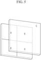
- FIG. 5 is a schematic top plan view of an organic CMOS image sensor according to some example embodiments and FIG. 6 is a cross-sectional view showing one example of the organic CMOS image sensor of FIG. 5 .
- the semiconductor substrate 110 may be a silicon substrate and is integrated with the photo-sensing devices 50a and 50b, the transmission transistor (not shown), and the charge storage 55.
- the photo-sensing devices 50a and 50b may be photodiodes.
- the lower insulation layer 60 is formed on the metal wire and the pad.
- the lower insulation layer 60 may be made of an inorganic insulating material such as a silicon oxide and/or a silicon nitride, or a low dielectric constant (low K) material such as SiC, SiCOH, SiCO, and SiOF.
- the lower insulation layer 60 has a trench exposing the charge storage 55. The trench may be filled with fillers.
- a color filter layer 70 is formed on the lower insulation layer 60.
- the color filter layer 70 includes a blue filter 70a formed in a blue pixel and a red filter 70b formed in a red pixel.
- a green filter is not included, but a green filter may be further included.
- the upper insulation layer 80 is formed on the color filter layer 70.
- the upper insulation layer 80 may eliminate a step caused by the color filter layer 70 and smoothen the surface.
- the upper insulation layer 80 and the lower insulation layer 60 may include a contact hole (not shown) exposing a pad, and a through-hole 85 ("trench") exposing the charge storage 55 of the green pixel.
- the photoelectric conversion device 100 is formed on the upper insulation layer 80.
- the photoelectric conversion device 100 includes the first electrode 10, the inorganic nanolayer 40, the photoelectric conversion layer 30, and the second electrode 20 as described above. Details are the same as described above.
- Focusing lens may be further formed on the photoelectric conversion device 100.
- the focusing lens may control a direction of incident light and gather the light in one region.
- the focusing lens may have a shape of, for example, a cylinder or a hemisphere, but is not limited thereto.
- FIG. 6 Even though the structure including the stacked photoelectric conversion device 100 of FIG. 1 is for example illustrated in FIG. 6 , a structure in which the photoelectric conversion device 200 of FIG. 2 is stacked may be applied in the same manner.
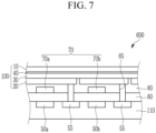
- FIG. 7 is a cross-sectional view showing another example of an organic CMOS image sensor.
- the organic CMOS image sensor 600 includes a semiconductor substrate 110 integrated with photo-sensing devices 50a and 50b, a transmission transistor (not shown), and a charge storage 55, a lower insulation layer 60, a color filter layer 70, an upper insulation layer 80, and a photoelectric conversion device 100.
- the positions of the first electrode 10 and the second electrode 20 are changed. That is, the first electrode 10 may be a light-receiving electrode.
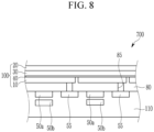
- FIG. 8 is a cross-sectional view showing another example of an organic CMOS image sensor.
- FIG. 8 Even though the structure including the stacked photoelectric conversion device 100 of FIG. 1 is for example illustrated in FIG. 8 , a structure in which the photoelectric conversion device 200 of FIG. 2 is stacked may be applied in the same manner.
- FIG. 9 is a cross-sectional view showing another example of an organic CMOS image sensor.
- an organic CMOS image sensor 800 includes a semiconductor substrate 110 integrated with photo-sensing devices 50a and 50b, a transmission transistor (not shown), and a charge storage 55, an upper insulation layer 80 having a through-hole 85, and a photoelectric conversion device 100.
- the positions of the first electrode 10 and the second electrode 20 are changed. That is, the first electrode 10 may be a light-receiving electrode.
- An organic CMOS image sensor 900 has a structure in which a green photoelectric conversion device selectively absorbing light in a green wavelength spectrum of light, a blue photoelectric conversion device selectively absorbing light in a blue wavelength spectrum of light, and a red photoelectric conversion device selectively absorbing light in a red wavelength spectrum of light are stacked.
- a metal wire (not shown) and a pad (not shown) are formed on the semiconductor substrate 110, and the lower insulation layer 60 is formed on the metal wire and the pad.
- the second photoelectric conversion device 100b includes a first electrode 10b and a second electrode 20b, and a photoelectric conversion layer 30b and an inorganic nanolayer 40b between the first electrode 10b and the second electrode 20b.
- the first electrode 10b, the second electrode 20b, the photoelectric conversion layer 30b, and the inorganic nanolayer 40b are the same as described above, and the photoelectric conversion layer 30b may selectively absorb light in one of red, blue, and green wavelength spectra of light.
- the first photoelectric conversion device 100b may be a blue photoelectric conversion device.
- the upper insulation layer 80 may be formed on the second photoelectric conversion device 100b.
- the lower insulation layer 60, the intermediate insulation layer 65, and the upper insulation layer 80 have a plurality of a plurality of through-holes exposing the charge storages 55a, 55b, and 55c.
- the third photoelectric conversion device 100c is formed on the upper insulation layer 80.
- the third photoelectric conversion device 100c includes a first electrode 10c and a second electrode 20c facing each other, and a photoelectric conversion layer 30c and an inorganic nanolayer 40c disposed between the first electrode 10c and the second electrode 20c.
- the first electrode 10c, the second electrode 20c, the photoelectric conversion layer 30c, and the inorganic nanolayer 40c are the same as described above, and the photoelectric conversion layer 30c may selectively absorb light in one of red, blue, and green wavelength spectra of light.
- the third photoelectric conversion device 100c may be a green photoelectric conversion device and may be the photoelectric conversion device 100.
- the first photoelectric conversion device 100a, the second photoelectric conversion device 100b, and the third photoelectric conversion device 100c are sequentially stacked, but the present disclosure is not limited thereto, and they may be stacked in various orders.
- the first photoelectric conversion device 100a, the second photoelectric conversion device 100b, and the third photoelectric conversion device 100c are stacked, and thus the size of an image sensor may be reduced to realize a down-sized image sensor.
- an organic CMOS image sensor 1100 may include a photoelectric conversion device 90 that itself includes a plurality of photoelectric conversion devices 90-1, 90-2, and 90-3 on a semiconductor substrate 110, where the plurality of photoelectric conversion devices 90-1, 90-2, and 90-3 are configured to convert different wavelength spectra of light (e.g., different ones of blue light, green light, or red light) into electric signals, respectively.
- the separate photoelectric conversion devices 90-1 to 90-3 may be horizontally arranged on the semiconductor substrate 110 such that the photoelectric conversion devices 90-1 to 90-3 are partially or entirely overlapped with each other in a direction that extends in parallel with a top surface 110a of the semiconductor substrate 110.
- each separate photoelectric conversion device 90-1 to 90-3 is connected to a separate charge storage 55 that is integrated into the semiconductor substrate 110 via a separate trench 85.
- FIG. 15 is a schematic cross-sectional view of an organic CMOS image sensor according to some example embodiments.
- an organic CMOS image sensor 1200 may include a semiconductor substrate 110 and photoelectric conversion devices 90-1 and 91 that are stacked on each other so as to at least partially overlap in a direction extending perpendicular to the top surface 110a of the semiconductor substrate 110, and wherein at least one of the photoelectric conversion devices 90-1 and 91 further includes multiple photoelectric conversion devices 90-2 and 90-3 that are arranged so as to overlap in a direction extending parallel to the top surface 110a of the semiconductor substrate 110, and where the plurality of photoelectric conversion devices 90-1, 90-2, and 90-3 are configured to convert different wavelength spectra of light (e.g., different ones of blue light, green light, or red light) into electric signals, respectively.
- different wavelength spectra of light e.g., different ones of blue light, green light, or red light
- photoelectric conversion device 90-1 includes multiple, horizontally-arranged photoelectric conversion devices configured to absorb different wavelengths spectra of light while photoelectric conversion device 91 is limited to a single photoelectric conversion device that is configured to absorb a single wavelength spectrum of light.
- an entirety of the photoelectric conversion device 91 overlaps a limited portion of the photoelectric conversion device 90-1 in the direction extending perpendicular to the top surface 110a and a remainder portion of the photoelectric conversion device 90-1 that is exposed by the photoelectric conversion device 91 is covered by insulation layer 80.
- an entirety of the photoelectric conversion device 90-1 overlaps a limited portion of the photoelectric conversion device 91 in the direction extending perpendicular to the top surface 110a.
- Other structures of organic CMOS image sensor 1200 are the same as one or more of the organic CMOS image sensors described with reference to any of FIGS. 3-12 .
- FIG. 16 is a schematic cross-sectional view of an organic CMOS image sensor according to some example embodiments.
- an organic CMOS image sensor 1300 includes a semiconductor substrate 110 integrated with photo-sensing devices 50a and 50b, a transmission transistor (not shown) and a charge storage 55, a lower insulation layer 60, and a color filter layer 70 on the semiconductor substrate 110, and a photoelectric conversion device 90 under the semiconductor substrate 110.
- the photoelectric conversion device 90 shown in FIG. 16 is any of the example embodiments of photoelectric conversion devices described herein. As shown in FIG. 16 , the photoelectric conversion device 90 may be on (e.g., above or beneath) the semiconductor substrate 110, such that the color filter layer 70 is distal from the photoelectric conversion device 90 in relation to the photo-sensing devices 50a and 50b.
- Other structures of organic CMOS image sensor 1300 are the same as one or more of the organic CMOS image sensors described with reference to any of FIGS. 3-12 .
- an organic CMOS image sensor includes a photo-sensing device and a photoelectric conversion device
- the photo-sensing device and the photoelectric conversion device may be configured to absorb different, first and second wavelength spectra of light and convert said absorbed light into electric signals.
- an organic CMOS image sensor may include one or more photo-sensing devices and may omit one or more color filters 70a, 70b overlapping the one or more photo-sensing devices in the direction extending perpendicular to the top surface 110a.
- Such one or more photo-sensing devices may be configured to sense light having a particular, limited wavelength spectrum of light in the absence of the light being filtered by a color filter prior to being received at the photo-sensing device. Accordingly, it will be understood that, in some example embodiments, the organic CMOS image sensors described herein according to various example embodiments may omit the color filters illustrated in said organic CMOS image sensors.
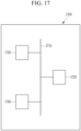
- an electronic device 1700 may include a processor 1720, a memory 1730, and an organic CMOS image sensor 1740 that are electrically coupled together via a bus 1710.
- the organic CMOS image sensor 1740 may be an organic CMOS image sensor of any of the example embodiments as described herein, and the organic CMOS image sensor included in the organic CMOS image sensor 1740 may include any of the photoelectric conversion devices described herein according to any of the example embodiments of the inventive concepts.
- the memory 1730 which may be a non-transitory computer readable medium, may store a program of instructions.
- the processor 1720 may execute the stored program of instructions to perform one or more functions.
- the processor 1720 may be configured to process electric signals generated by the organic CMOS image sensor 1740.
- the processor 1720 may be configured to generate an output (e.g., an image to be displayed on a display interface) based on processing the electric signals.
- a 150 nm-thick anode is formed by sputtering ITO on a glass substrate.
- a 5 nm-thick charge auxiliary layer is formed by depositing a compound represented by Chemical Formula A.
- a 100 nm-thick photoelectric conversion layer is formed by codepositing a p-type semiconductor ( ⁇ max : 545 nm) represented by Chemical Formula B-1 and an n-type semiconductor, fullerene C60, in a volume ratio of 1:1.
- a 1.5 nm-thick inorganic nanolayer is formed by thermally depositing Yb (WF: 2.6 eV).
- a 7 nm-thick cathode is formed by sputtering ITO (WF: 4.7 eV).
- a 50 nm-thick anti-reflection layer is formed by depositing aluminum oxide (Al 2 O 3 ), and then, a glass plate is used for sealing to manufacture a photoelectric conversion device.
- a photoelectric conversion device is manufactured according to the same method as Example 1 except that the p-type semiconductor and the n-type semiconductor are codeposited in a volume ratio of 1.2:1 to form a 90 nm-thick photoelectric conversion layer.
- the photoelectric conversion efficiency (EQE) is evaluated in a wavelength spectrum of light of 400 nm to 720 nm in an Incident Photon to Current Efficiency (IPCE) method. The results are shown in Tables 4 and 5. (Table 4) Photoelectric conversion efficiency (EQE, %) Example 1 72.3 Comparative Example 1 70.7 (Table 5) Photoelectric conversion efficiency (EQE, %) Example 3 61.3 Comparative Example 3 60.0
Landscapes
- Physics & Mathematics (AREA)
- Electromagnetism (AREA)
- Chemical & Material Sciences (AREA)
- Inorganic Chemistry (AREA)
- Engineering & Computer Science (AREA)
- Materials Engineering (AREA)
- Light Receiving Elements (AREA)
- Photovoltaic Devices (AREA)
- Solid State Image Pick-Up Elements (AREA)
Description
- Photoelectric conversion devices, organic sensors, and electronic devices are disclosed.
- A photoelectric conversion device may receive incident light and converts the received incident light into an electric signal. A photoelectric conversion device may include a photodiode and a phototransistor, and may be applied to ("included in") an organic sensor, a photodetector, a solar cell, or the like.
- Organic sensors may have higher resolutions and thus may have smaller pixel sizes. Organic sensors may include silicon photodiodes. A sensitivity of a silicon photodiode in an organic sensor may be deteriorated based on reduced pixel size of the organic sensor, as the absorption area of the silicon photodiode may be reduced. Accordingly, organic materials that are capable of replacing silicon in photodiodes of organic sensors have been researched.
- An organic material has a high extinction coefficient and is configured to selectively absorb light in a particular wavelength spectrum of light depending on a molecular structure of the organic material, and thus may simultaneously replace a photodiode and a color filter of an organic sensor and resultantly improve sensitivity of the organic sensor and contribute to high integration of the organic sensor.
- However, since such organic materials exhibit different characteristics from those of silicon due to high binding energy and a recombination behavior associated with such organic materials, the characteristics of the organic materials are difficult to precisely predict, and thus required properties of a photoelectric conversion device may not be easily controlled.
-
US 2014/070183 discloses an organic photoelectric device including a first electrode, a metal nanolayer contacting one side of the first electrode, an active layer on one side of the metal nanolayer, and a second electrode on one side of the active layer. -
US 2017/294485 discloses an imaging device, a manufacturing device, and a manufacturing method capable of preventing a substance such as hydrogen from entering and preventing change in performance. -
EP 2 706 586 discloses a transmissive electrode including a light transmission layer. -
US 2016/380221 discloses a photoelectric conversion element including a first interconnect, a second interconnect, a photoelectric conversion layer and an insulating layer. -
US 2016/118609 discloses a solar cell including a substrate and a stacked body. - Some example embodiments provide one or more photoelectric conversion devices capable of improving charge extraction efficiency.
- Some example embodiments provide organic sensors including one or more of the photoelectric conversion device.
- Some example embodiments provide electronic devices including the one or more photoelectric conversion devices or the one or more organic sensors.
- According to an aspect of the invention, a photoelectric conversion device is provided in accordance with claim 1.
- The first electrode may include a transparent electrode having a light transmittance of greater than or equal to 80 %, or a reflective electrode having a light transmittance of less than 10 %.
- The first electrode may include the transparent electrode, and the transparent electrode includes at least one of an oxide conductor and a carbon conductor.
- The thickness of the inorganic nanolayer is less than or equal to 5 nm.
- The thickness of the inorganic nanolayer may be less than or equal to 2 nm.
- The first electrode may be a cathode and the second electrode is an anode.
- A difference between the work function of the conductor and the effective work function at the surface of the first electrode facing the photoelectric conversion layer may be greater than or equal to 0.5 eV.
- The work function of the conductor may be greater than or equal to 4.5 eV, and the effective work function at the surface of the first electrode facing the photoelectric conversion layer may be less than or equal to 4.0 eV.
- The effective work function at the surface of the first electrode facing the photoelectric conversion layer may be less than or equal to 3.0 eV.
- The transparent conductor may include an oxide conductor or a carbon conductor.
- The inorganic nanolayer may have a thickness of less than or equal to 2 nm. The first electrode may be a cathode and the second electrode may be an anode.
- An electronic device may include the photoelectric conversion device.
- An organic sensor may include the photoelectric conversion device. The organic sensor may be an organic complementary metal-oxide-semiconductor (CMOS) sensor. An electronic device may include the organic sensor such as the organic CMOS image sensor.
-
-
FIG. 1 is a cross-sectional view showing a photoelectric conversion device according to some example embodiments, -
FIG. 2 is a cross-sectional view showing a photoelectric conversion device according to some example embodiments. -
FIG. 3 is a cross-sectional view showing an example of an organic CMOS image sensor according to some example embodiments, -
FIG. 4 is a cross-sectional view showing another example of an organic CMOS image sensor according to some example embodiments, -
FIG. 5 is a schematic top plan view of an organic CMOS image sensor according to some example embodiments, -
FIG. 6 is a cross-sectional view showing an example of the organic CMOS image sensor ofFIG. 5 , -
FIG. 7 is a cross-sectional view showing another example of an organic CMOS image sensor, -
FIG. 8 is a cross-sectional view showing another example of an organic CMOS image sensor, -
FIG. 9 is a cross-sectional view showing another example of an organic CMOS image sensor, -
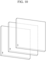
FIG. 10 is a schematic top plan view of an organic CMOS image sensor according to some example embodiments, -
FIG. 11 is a cross-sectional view of the organic CMOS image sensor ofFIG. 10 , -
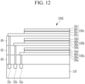
FIG. 12 is a cross-sectional view showing another example of an organic CMOS image sensor -
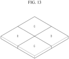
FIG. 13 is a schematic top plan view showing an example of an organic CMOS image sensor according to some example embodiments, andFIG. 14 is a schematic cross-sectional view showing an example of the organic CMOS image sensor ofFIG. 13 , -
FIG. 15 is a schematic cross-sectional view of an organic CMOS image sensor according to some example embodiments, -
FIG. 16 is a schematic cross-sectional view of an organic CMOS image sensor according to some example embodiments, and -
FIG. 17 is a schematic diagram of an electronic device according to some example embodiments. - Hereinafter, example embodiments of the present disclosure will be described in detail so that a person skilled in the art would understand the same. However, this disclosure may be embodied in many different forms and is not to be construed as limited to the example embodiments set forth herein.
- In the drawings, the thickness of layers, films, panels, regions, etc., are exaggerated for clarity.
- It will be understood that when an element such as a layer, film, region, or substrate is referred to as being "on" another element, it may be directly on the other element or intervening elements may also be present. In contrast, when an element is referred to as being "directly on" another element, there are no intervening elements present.
- As used herein, when a definition is not otherwise provided, "substituted" may refer to replacement of a hydrogen atom of a compound or group by a substituent selected from a halogen atom, a hydroxy group, an alkoxy group, a nitro group, a cyano group, an amino group, an azido group, an amidino group, a hydrazino group, a hydrazono group, a carbonyl group, a carbamyl group, a thiol group, an ester group, a carboxyl group or a salt thereof, a sulfonic acid group or a salt thereof, phosphoric acid group or a salt thereof, silyl group, a C1 to C20 alkyl group, a C2 to C20 alkenyl group, a C2 to C20 alkynyl group, a C6 to C30 aryl group, a C7 to C30 arylalkyl group, a C1 to C30 alkoxy group, a C1 to C20 heteroalkyl group, a C3 to C20 heteroaryl group, a C3 to C20 heteroarylalkyl group, a C3 to C30 cycloalkyl group, a C3 to C15 cycloalkenyl group, a C6 to C15 cycloalkynyl group, a C3 to C30 heterocycloalkyl group, and a combination thereof.
- As used herein, when a definition is not otherwise provided, "hetero" may refer to one including 1 to 4 heteroatoms selected from N, O, S, Se, Te, Si, and P.
- As used herein, when a definition is not otherwise provided, "heterocyclic group" is a generic concept of a heteroaryl group, may include an aromatic and nonaromatic ring including at least one heteroatom, and may include at least one heteroatom selected from N, O, S, P, and Si instead of carbon (C) in a cyclic group such as an aryl group, a cycloalkyl group, a fused ring thereof, or a combination thereof. When the heterocyclic group is a fused ring, the entire ring or each ring of the heterocyclic group may include one or more heteroatoms.
- Hereinafter, "combination" may refer to a mixture of two or more and a stack structure of two or more.
- Hereinafter, "metal" may refer to metal, semi-metal, or a combination thereof.
- Hereinafter, a work function or an energy level is expressed as an absolute value from a vacuum level. In addition, when the work function or the energy level is referred to be deep, high, or large, it may have a large absolute value from "0 eV" of the vacuum level while when the work function or the energy level is referred to be shallow, low, or small, it may have a small absolute value from "0 eV" of the vacuum level.
- Hereinafter, a photoelectric conversion device according to some example embodiments is described.
-
FIG. 1 is a cross-sectional view showing a photoelectric conversion device according to some example embodiments. - Referring to
FIG. 1 , aphotoelectric conversion device 100 according to some example embodiments includes afirst electrode 10, asecond electrode 20, aphotoelectric conversion layer 30, and aninorganic nanolayer 40. - A substrate (not shown) may be disposed at the side of the
first electrode 10 or thesecond electrode 20. The substrate may be for example made of an inorganic material such as glass, an organic material such as polycarbonate, polymethylmethacrylate, polyethyleneterephthalate, polyethylenenaphthalate, polyamide, polyethersulfone, or a combination thereof, or a silicon wafer. The substrate may be omitted. - As shown, the
first electrode 10 and thesecond electrode 20 are facing each other. One of thefirst electrode 10 and thesecond electrode 20 is an anode and the other is a cathode. In some example embodiments, thefirst electrode 10 may be a cathode and thesecond electrode 20 may be an anode. In another example, thefirst electrode 10 may be an anode and thesecond electrode 20 may be a cathode. - At least one of the
first electrode 10 and thesecond electrode 20 may be a transparent electrode, such that the at least one of thefirst electrode 10 and thesecond electrode 20 includes a transparent conductor. Herein, the transparent electrode may include a transparent conductor having a high light transmittance of greater than or equal to 80 % and may not include for example a semi-transparent electrode for microcavity. The transparent electrode may include for example a transparent conductor that includes at least one of an oxide conductor and a carbon conductor. The oxide conductor may include for example at least one of indium tin oxide (ITO), indium zinc oxide (IZO), zinc tin oxide (ZTO), aluminum tin oxide (AlTO), and aluminum zinc oxide (AZO) and the carbon conductor may include at least one of graphene and carbon nanostructure. - One of the
first electrode 10 and thesecond electrode 20 may be a reflective electrode, such that the at least one of thefirst electrode 10 and thesecond electrode 20 includes a reflective conductor. Here, the reflective electrode may include, in some example embodiments, a reflective conductor having a light transmittance of less than about 10 % or high reflectance of more than or equal to about 5 %. The reflective electrode may include a reflective conductor such as a metal and may include, for example aluminum (Al), silver (Ag), gold (Au), or an alloy thereof. - In view of the above, it will be understood that the
first electrode 10 and/or thesecond electrode 20 does include a conductor, where the conductor may be a transparent conductor or a reflective conductor. A conductor that is a transparent conductor may have a light transmittance of greater than or equal to about 80 %. A conductor that is a reflective conductor may have a light transmittance of less than about 10 %. - When the terms "about" or "substantially" are used in this specification in connection with a numerical value, it is intended that the associated numerical value include a tolerance of ±10% around the stated numerical value. When ranges are specified, the range includes all values therebetween such as increments of 0.1%.
- In some example embodiments, the
first electrode 10 may be a transparent electrode having a light transmittance of greater than or equal to 80 % or a reflective electrode having a light transmittance of less than 10 %. - The
photoelectric conversion layer 30, which, as shown, is between thefirst electrode 10 and thesecond electrode 20, is configured to absorb light in at least one part of a wavelength spectrum of light and convert the absorbed light into an electric signal, and for example one of light in a green wavelength spectrum of light (hereinafter, referred to as "green light"), light in a blue wavelength spectrum of light (hereinafter, referred to as "blue light"), light in a red wavelength spectrum of light (hereinafter, referred to as "red light") , light in an ultraviolet wavelength spectrum of light (hereinafter, referred to as 'ultraviolet light'), and light in an infrared wavelength spectrum of light (hereinafter, referred to as "infrared light") into an electric signal. - In some example embodiments, the
photoelectric conversion layer 30 may be configured to selectively absorb at least one of the green light, the blue light, the red light, and the infrared light. Herein, the selective absorption of at least one from the green light, the blue light, the red light, and the infrared light means that a light-absorption spectrum has a peak absorption wavelength (λmax) in one of about 500 nm to about 600 nm, greater than or equal to about 380 nm and less than about 500 nm, greater than about 600 nm and less than or equal to about 700 nm, and greater than about 700 nm, and a light-absorption spectrum in the corresponding wavelength spectrum of light may be remarkably higher than those in the other wavelength spectra of light. - The
photoelectric conversion layer 30 may include a semiconductor material that is at least one p-type semiconductor and/or at least one n-type semiconductor, where the semiconductor material forms a pn junction with the first organic material of thephotoelectric conversion layer 30 and may produce excitons by receiving light from outside and then separate the produced excitons into holes and electrons. - The p-type semiconductor and the n-type semiconductor may be independently light-absorbing materials, and for example at least one of the p-type semiconductor and the n-type semiconductor may be an organic light-absorbing material. In some example embodiments, at least one of the p-type semiconductor and the n-type semiconductor may be a wavelength-selective light-absorbing material that selectively absorbs light in a particular (or, alternatively, predetermined) wavelength spectrum of light, and for example at least one of the p-type semiconductor and the n-type semiconductor may be a wavelength-selective organic light-absorbing material. The p-type semiconductor and the n-type semiconductor may have a peak absorption wavelength (λmax) in the same wavelength spectrum of light or in a different wavelength spectrum of light.
- In some example embodiments, the p-type semiconductor may be an organic material having a core structure including an electron donating moiety, a pi conjugation linking group, and an electron accepting moiety.
- The p-type semiconductor may be for example represented by Chemical Formula 1, but is not limited thereto.
[Chemical Formula 1] EDG - HA - EAG
In Chemical Formula 1, - HA is a C2 to C30 heterocyclic group having at least one of S, Se, Te, and Si,
- EDG is an electron-donating group, and
- EAG is an electron accepting group.
- In some example embodiments, the p-type semiconductor represented by Chemical Formula 1 may be for example represented by Chemical Formula 1A.

- In Chemical Formula 1A,
X may be S, Se, Te, SO, SO2, or SiRaRb, - Ar may be a substituted or unsubstituted C6 to C30 arylene group, a substituted or unsubstituted C3 to C30 heterocyclic group, or a fused ring of the foregoing two or more,
- Ar1a and Ar2a may independently be a substituted or unsubstituted C6 to C30 aryl group or a substituted or unsubstituted C3 to C30 heteroaryl group,
- Ar1a and Ar2a may independently be present alone or may be linked with each other to form a fused ring, and
- R1a to R3a, Ra, and Rb may independently be hydrogen, deuterium, a substituted or unsubstituted C1 to C30 alkyl group, a substituted or unsubstituted C6 to C30 aryl group, a substituted or unsubstituted C3 to C30 heteroaryl group, a substituted or unsubstituted C1 to C6 alkoxy group, a halogen, or a cyano group.
- In some example embodiments, in Chemical Formula 1A, Ar1a and Ar2a may independently be one of a substituted or unsubstituted phenyl group, a substituted or unsubstituted naphthyl group, a substituted or unsubstituted anthracenyl group, a substituted or unsubstituted phenanthrenyl group, a substituted or unsubstituted pyridinyl group, a substituted or unsubstituted pyridazinyl group, a substituted or unsubstituted pyrimidinyl group, a substituted or unsubstituted pyrazinyl group, a substituted or unsubstituted quinolinyl group, a substituted or unsubstituted isoquinolinyl group, a substituted or unsubstituted naphthyridinyl group, a substituted or unsubstituted cinnolinyl group, a substituted or unsubstituted quinazolinyl group, a substituted or unsubstituted phthalazinyl group, a substituted or unsubstituted benzotriazinyl group, a substituted or unsubstituted pyridopyrazinyl group, a substituted or unsubstituted pyridopyrimidinyl group, and a substituted or unsubstituted pyridopyridazinyl group.
- In some example embodiments, Ar1a and Ar2a of Chemical Formula 1A may be linked with each other to form a ring or in some example embodiments, Ar1a and Ar2a may be linked with each other by one of a single bond, -(CRgRh)n2- (n2 is 1 or 2), -O-, -S-, -Se-, -N=, -NRi-, -SiRjRk-, and -GeRlRm- to form a ring. Herein, Rg to Rm may independently be hydrogen, a substituted or unsubstituted C1 to C30 alkyl group, a substituted or unsubstituted C6 to C30 aryl group, a substituted or unsubstituted C3 to C30 heteroaryl group, a substituted or unsubstituted C1 to C6 alkoxy group, a halogen, or a cyano group.
- In some example embodiments, the p-type semiconductor represented by Chemical Formula 1 may be for example represented by Chemical Formula 1B.

- In Chemical Formula 1B,
X1 may be Se, Te, O, S, SO, or SO2, - Ar3 may be a substituted or unsubstituted C6 to C30 arylene group, a substituted or unsubstituted C3 to C30 heterocyclic group, or a fused ring of the foregoing two or more,
- R1 to R3 may independently be one of hydrogen, deuterium, a substituted or unsubstituted C1 to C30 alkyl group, a substituted or unsubstituted C1 to C30 alkoxy group, a substituted or unsubstituted C6 to C30 aryl group, a substituted or unsubstituted C3 to C30 heteroaryl group, a halogen, a cyano group, a cyano-containing group, and a combination thereof,
- G may be one of a single bond, -O-, -S-, -Se-, -N=, -(CRfRg)k-, -NRh-, -SiRiRj-, -GeRkRl-, -(C(Rm)=C(Rn))-, and SnRoRp, wherein Rf, Rg, Rh, Ri, Rj, Rk, Rl, Rm, Rn, Ro, and Rp may independently be one of hydrogen, a halogen, a substituted or unsubstituted C1 to C10 alkyl group, a substituted or unsubstituted C1 to C10 alkoxy group, and a substituted or unsubstituted C6 to C12 aryl group, Rf and Rg, Ri and Rj, Rk and Rl, Rm and Rn, and Ro and Rp may independently be present alone or may be linked with each other to provide a ring, and k may be 1 or 2,
- R6a to R6d and R7a to R7d may independently be one of hydrogen, a substituted or unsubstituted C1 to C30 alkyl group, a substituted or unsubstituted C6 to C30 aryl group, a substituted or unsubstituted C3 to C30 heteroaryl group, a halogen, a cyano group, a cyano-containing group, and a combination thereof,
- R6a to R6d may independently be present alone or adjacent two thereof may be linked with each other to form a fused ring, and
- R7a to R7d may independently be present alone or adjacent two thereof may be linked with each other to form a fused ring.
- In some example embodiments, Ar3 of Chemical Formula 1B may be benzene, naphthylene, anthracene, thiophene, selenophene, tellurophene, pyridine, pyrimidine, or a fused ring of the foregoing two or more.
- The n-type semiconductor may be for example fullerene or a fullerene derivative, but is not limited thereto.
- The
photoelectric conversion layer 30 may be an intrinsic layer (an I layer) wherein the p-type semiconductor and the n-type semiconductor are mixed as a bulk heterojunction. Herein, the p-type semiconductor and the n-type semiconductor may be mixed in a volume ratio of about 1:9 to about 9:1, for example about 2:8 to about 8:2, about 3:7 to about 7:3, about 4:6 to about 6:4, or about 5:5. - The
photoelectric conversion layer 30 may be a bilayer including a p-type layer including the p-type semiconductor and an n-type layer including the n-type semiconductor. Herein, a thickness ratio of the p-type layer and the n-type layer may be about 1:9 to about 9:1, for example about 2:8 to about 8:2, about 3:7 to about 7:3, about 4:6 to about 6:4, or about 5:5. - The
photoelectric conversion layer 30 may further include a p-type layer and/or an n-type layer in addition to the intrinsic layer. The p-type layer may include the p-type semiconductor and the n-type layer may include the n-type semiconductor. In some example embodiments, they may be included in various combinations of p-type layer/I layer, I layer/n-type layer, p-type layer/I layer/n-type layer, and the like. - The
inorganic nanolayer 40 is disposed between thefirst electrode 10 and thephotoelectric conversion layer 30 and is in contact with thefirst electrode 10 and with thephotoelectric conversion layer 30. As shown inFIG. 1 , thesurface 10s of thefirst electrode 10 that faces thephotoelectric conversion layer 30 is covered by theinorganic nanolayer 40. One surface of theinorganic nanolayer 40 is in contact with thefirst electrode 10 and another, opposite surface of theinorganic nanolayer 40 is in contact with thephotoelectric conversion layer 30. - The
inorganic nanolayer 40 has a thickness less than or equal to 5 nm, preferably less than or equal to about 3 nm, or less than or equal to 2 nm. Theinorganic nanolayer 40 may have, for example a thickness of about 1 nm to 5 nm, about 1 nm to about 3 nm, or about 1 nm to 2 nm. - The
inorganic nanolayer 40 includes ytterbium (Yb) and may have a lower work function than thefirst electrode 10. In some example embodiments, a work function of theinorganic nanolayer 40 may be less than a work function of thefirst electrode 10 by about 0.5 eV or greater. Restated, a difference between the work function of the conductor (e.g., the transparent conductor or the reflective conductor) of thefirst electrode 10 and the effective work function at thesurface 10s of thefirst electrode 10 facing thephotoelectric conversion layer 30 may be greater than or equal to about 0.5 eV. In some example embodiments, the work function of the first electrode 10 (e.g., the work function of the conductor (e.g., transparent conductor or reflective conductor) of the first electrode 10) may be greater than or equal to about 4.5 eV and the work function of theinorganic nanolayer 40 may be less than or equal to about 4.0 eV. In some example embodiments, the work function of thefirst electrode 10 may be greater than or equal to about 4.5 eV and the work function of theinorganic nanolayer 40 may be less than or equal to about 3.5 eV. In some example embodiments, the work function of thefirst electrode 10 may be greater than or equal to about 4.5 eV and the work function of theinorganic nanolayer 40 may be less than or equal to about 3.0 eV. In some example embodiments, the work function of thefirst electrode 10 may be greater than or equal to about 4.5 eV and the work function of theinorganic nanolayer 40 may be less than or equal to about 2.8 eV. In some example embodiments, the work function of thefirst electrode 10 may be about 4.5 eV to about 5.0 eV and the work function of theinorganic nanolayer 40 may be about 1.5 eV to about 4.0 eV, about 1.5 eV to about 3.5 eV, about 1.5 eV to about 3.0 eV, or about 1.5 eV to about 2.8 eV. - In some example embodiments, the
inorganic nanolayer 40 may be formed by thermal evaporation. Since theinorganic nanolayer 40 is formed by thermal evaporation as described above, it is possible to prevent thephotoelectric conversion layer 30 from being thermally and physically damaged in its formation process and/or the subsequent process of theinorganic nanolayer 40, and thus to prevent its performance from being deteriorated due to degradation of thephotoelectric conversion layer 30, thereby improving the performance of thephotoelectric conversion device 100. - The inorganic material that satisfies such characteristics is ytterbium (Yb).
- As described above, the
inorganic nanolayer 40 is in contact with the surface of thefirst electrode 10 between thefirst electrode 10 and thephotoelectric conversion layer 30, and it may have a thin thickness compared with thefirst electrode 10. Accordingly, theinorganic nanolayer 40 may function as a surface-treatment layer of thefirst electrode 10 on the surface of thefirst electrode 10 facing thephotoelectric conversion layer 30 and controls the effective work function of thefirst electrode 10 on the surface of thefirst electrode 10 facing thephotoelectric conversion layer 30. Herein, the effective work function is the work function at the interface of the two layers in a structure where the two layers having different electrical characteristics are in contact with each other. The effective work function of thefirst electrode 10 at the interface of thefirst electrode 10 and thephotoelectric conversion layer 30 is controlled by the very-thininorganic nanolayer 40 and is a combined work function of thefirst electrode 10 and theinorganic nanolayer 40. - In some example embodiments, the effective work function on the surface of the
first electrode 10 facing thephotoelectric conversion layer 30 may be different from the work function of the conductor (e.g., the transparent conductor or the reflective conductor) of thefirst electrode 10 based on the influences of theinorganic nanolayer 40. In some example embodiments, the effective work function on the surface of thefirst electrode 10 facing thephotoelectric conversion layer 30 may be less than the work function of the conductor (e.g., the transparent conductor or the reflective conductor) of thefirst electrode 10. The effective work function on the surface of thefirst electrode 10 facing thephotoelectric conversion layer 30 may be the same as the work function of theinorganic nanolayer 40 or may be a medium value between the work function of theinorganic nanolayer 40 and the work function of thefirst electrode 10. - In some example embodiments, the work function of the conductor (e.g., transparent conductor or reflective conductor) of the
first electrode 10 may be greater than or equal to about 4.5 eV and an effective work function on ("at") the surface of thefirst electrode 10 may be less than or equal to about 4.0 eV. In some example embodiments, the work function of the conductor (e.g., transparent conductor or reflective conductor) of thefirst electrode 10 may be greater than or equal to about 4.5 eV and the effective work function on ("at") the surface of thefirst electrode 10 may be less than or equal to about 3.5 eV. In some example embodiments, the work function of the conductor (e.g., the transparent conductor or the reflective conductor) of thefirst electrode 10 may be greater than or equal to about 4.5 eV, the effective work function on ("at") thesurface 10s of thefirst electrode 10 facing thephotoelectric conversion layer 30 may be less than or equal to about 3.0 eV. In some example embodiments, the work function of the conductor (e.g., transparent conductor or reflective conductor) of thefirst electrode 10 may be greater than or equal to about 4.5 eV and the effective work function on ("at") the surface of thefirst electrode 10 may be less than or equal to about 2.8 eV. In some example embodiments, the work function of the conductor (e.g., transparent conductor or reflective conductor) of thefirst electrode 10 may be about 4.5 eV to about 5.0 eV and the effective work function on ("at") the surface of thefirst electrode 10 may be about 1.5 eV to about 4.0 eV, about 1.5 eV to about 3.5 eV, about 1.5 eV to about 3.0 eV, or about 1.5 eV to about 2.8 eV. - By lowering the work function on ("at") the surface of the
first electrode 10 facing thephotoelectric conversion layer 30 as described above, extraction of charges (e.g., electrons) from thephotoelectric conversion layer 30 and moving to thefirst electrode 10 may be further facilitated, and remaining charge carriers may be further reduced to show higher charge extraction efficiency, thereby improving the performance of thephotoelectric conversion device 100. - The
photoelectric conversion device 100 may further include an anti-reflection layer (not shown) on one surface of thefirst electrode 10 or thesecond electrode 20. The anti-reflection layer is disposed at a light incidence side and lowers reflectance of light of incident light and thereby light absorbance is further improved, thereby improving performance of an organic complementary metal-oxide-semiconductor (CMOS) image sensor that includes thephotoelectric conversion device 100. In some example embodiments, when light is incident to thefirst electrode 10, the anti-reflection layer may be disposed on one surface of thefirst electrode 10, and when light is incident to thesecond electrode 20, anti-reflection layer may be disposed on one surface of thesecond electrode 20. - The anti-reflection layer may include, for example a material having a refractive index of about 1.6 to about 2.5 and may include for example at least one of metal oxide, metal sulfide, and an organic material having a refractive index within the ranges. The anti-reflection layer may include, for example a metal oxide such as aluminum-containing oxide, molybdenum-containing oxide, tungsten-containing oxide, vanadium-containing oxide, rhenium-containing oxide, niobium-containing oxide, tantalum-containing oxide, titanium-containing oxide, nickel-containing oxide, copper-containing oxide, cobalt-containing oxide, manganese-containing oxide, chromium-containing oxide, tellurium-containing oxide, or a combination thereof; metal sulfide such as zinc sulfide; or an organic material such as an amine derivative, but is not limited thereto.
- In the
photoelectric conversion device 100, when light enters from thefirst electrode 10 or thesecond electrode 20 and thephotoelectric conversion layer 30 absorbs light in a particular (or, alternatively, predetermined) wavelength spectrum of light, excitons may be produced thereinside. The excitons are separated into holes and electrons in thephotoelectric conversion layer 30, and the separated holes are transported to an anode that is one of thefirst electrode 10 and thesecond electrode 20 and the separated electrons are transported to the cathode that is the other of thefirst electrode 10 and thesecond electrode 20 so as to flow a current. - Hereinafter, a photoelectric conversion device according to some example embodiments is described.
-
FIG. 2 is a cross-sectional view showing a photoelectric conversion device according to some example embodiments. - Referring to
FIG. 2 , aphotoelectric conversion device 200 according to some example embodiments includes afirst electrode 10, asecond electrode 20, aphotoelectric conversion layer 30, and aninorganic nanolayer 40. - However, the
photoelectric conversion device 200 according to some example embodiments includes a chargeauxiliary layer 45 between thesecond electrode 20 and thephotoelectric conversion layer 30. The chargeauxiliary layer 45 may enhance efficiency by facilitating movement of charges (e.g., holes) separated from thephotoelectric conversion layer 30. - The charge
auxiliary layer 45 may include, for example an organic material, an inorganic material, or an organic/inorganic material. The organic material may be an organic compound having hole or electron characteristics and the inorganic material may be, for example metal oxide such as molybdenum oxide, tungsten oxide, or nickel oxide. - The charge
auxiliary layer 45 may include for example a visible light non-absorbing material that does not absorb light in a visible region substantially, for example a visible light non-absorbing organic material. - In some example embodiments, the visible light non-absorbing material may be a compound represented by Chemical Formula 2A or 2B but is not limited thereto.


- In Chemical Formula 2A or 2B,
M1 and M2 may independently be CRnRo, SiRpRq, NRr, O, S, Se, or Te, - Ar1b, Ar2b, Ar3b, and Ar4b may independently be a substituted or unsubstituted C6 to C30 aryl group or a substituted or unsubstituted C3 to C30 heteroaryl group,
- G2 and G3 may independently be a single bond, -(CRsRt)n3 -, -O-, -S-, -Se-, - N=, -NRu-, -SiRvRw-, or -GeRxRy-, wherein n3 is 1 or 2, and
- R30 to R37 and Rn to Ry may independently be hydrogen, a substituted or unsubstituted C1 to C30 alkyl group, a substituted or unsubstituted C6 to C30 aryl group, a substituted or unsubstituted C3 to C30 heterocyclic group, a substituted or unsubstituted C1 to C6 alkoxy group, a halogen, or a cyano group.
- In some example embodiments, the visible light non-absorbing material may be a compound represented by Chemical Formula 2A-1 or 2B-1, but is not limited thereto.


- In Chemical Formula 2A-1 or 2B-1,
M1, M2, G2, G3, and R30 to R37 are the same as described above, and
R38 to R45 may independently be hydrogen, a substituted or unsubstituted C1 to C30 alkyl group, a substituted or unsubstituted C6 to C30 aryl group, a substituted or unsubstituted C3 to C30 heteroaryl group, a substituted or unsubstituted C1 to C6 alkoxy group, a halogen, or a cyano group. - In some example embodiments, the visible light non-absorbing material may be a compound represented by Chemical Formula 2A-1a or 2B-1a but is not limited thereto.


- In Chemical Formula 2A-1a or 2B-1a, R38 to R45 and Ro, and Rn are the same as described above.
- The
photoelectric conversion devices - The
photoelectric conversion devices - Hereinafter, an example of an image sensor including the photoelectric conversion device will be described with reference to the drawings. As an example of an image sensor, an organic CMOS image sensor is described.
-
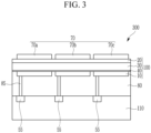
FIG. 3 is a cross-sectional view showing an example of an organic CMOS image sensor according to some example embodiments. - Referring to
FIG. 3 , an organicCMOS image sensor 300 according to some example embodiments includes asemiconductor substrate 110, aninsulation layer 80, aphotoelectric conversion device 100, and acolor filter layer 70. - The
semiconductor substrate 110 may be a silicon substrate, and is integrated with the transmission transistor (not shown) and thecharge storage 55. The transmission transistor and/or thecharge storage 55 may be integrated in each pixel. - A metal wire (not shown) and a pad (not shown) are formed on the
semiconductor substrate 110. In order to decrease signal delay, the metal wire and pad may be made of a metal having low resistivity, for example, aluminum (Al), copper (Cu), silver (Ag), and alloys thereof, but are not limited thereto. - The
insulation layer 80 is formed on the metal wire and the pad. Theinsulation layer 80 may be made of an inorganic insulating material such as a silicon oxide and/or a silicon nitride, or a low dielectric constant (low K) material such as SiC, SiCOH, SiCO, and SiOF. Theinsulation layer 80 has atrench 85 exposing thecharge storage 55. Thetrench 85 may be filled with fillers. - The
photoelectric conversion device 100 is formed on theinsulation layer 80. Thephotoelectric conversion device 100 includes afirst electrode 10, aninorganic nanolayer 40, aphotoelectric conversion layer 30, and asecond electrode 20 as described above. Details thereof are the same as described above. - A
color filter layer 70 is formed on thephotoelectric conversion device 100. Thecolor filter layer 70 includes ablue filter 70a formed in a blue pixel, ared filter 70b formed in a red pixel, and agreen filter 70c formed in a green pixel. However, thecolor filter layer 70 may include a cyan filter, a magenta filter, and/or a yellow filter instead of the above color filters or may further include them in addition to the above color filters. It will be understood that a color filter is configured to selectively transmit a particular wavelength spectrum of light. Where a color filter overlaps a photo-sensing device, the color filter may be configured to selectively transmit a particular wavelength spectrum of light to a photo-sensing device so that the photo-sensing device is configured to absorb, and convert into electrical signals, the particular wavelength spectrum of light. - Focusing lens (not shown) may be further formed on the
color filter layer 70. The focusing lens may control a direction of incident light and gather the light in one region. The focusing lens may have a shape of, for example, a cylinder or a hemisphere, but is not limited thereto. - Even though the structure including the stacked
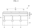
photoelectric conversion device 100 ofFIG. 1 is for example illustrated inFIG. 4 , structures in which thephotoelectric conversion device 200 ofFIG. 2 are stacked may be applied in the same manner. -
FIG. 4 is a cross-sectional view showing another example of an organic CMOS image sensor according to some example embodiments. - Referring to
FIG. 4 , an organicCMOS image sensor 400 according to some example embodiments includes asemiconductor substrate 110 integrated with a transmission transistor (not shown) and acharge storage 55, aninsulation layer 80, aphotoelectric conversion device 100, and acolor filter layer 70. - However, in the organic
CMOS image sensor 400 according to some example embodiments, the positions of thefirst electrode 10 and thesecond electrode 20 of thephotoelectric conversion device 100 are changed. That is, thefirst electrode 10 may be a light-receiving electrode. - Even though the structure including the stacked
photoelectric conversion device 100 ofFIG. 1 is for example illustrated inFIG. 6 , structures in which thephotoelectric conversion device 200 ofFIG. 2 are stacked may be applied in the same manner. -
FIG. 5 is a schematic top plan view of an organic CMOS image sensor according to some example embodiments andFIG. 6 is a cross-sectional view showing one example of the organic CMOS image sensor ofFIG. 5 . - Referring to
FIGS. 5 and6 , an organicCMOS image sensor 500 according to some example embodiments includes asemiconductor substrate 110 integrated with photo-sensing devices charge storage 55, alower insulation layer 60, acolor filter layer 70, anupper insulation layer 80, and aphotoelectric conversion device 100. - The
semiconductor substrate 110 may be a silicon substrate and is integrated with the photo-sensing devices charge storage 55. The photo-sensing devices - The photo-
sensing devices charge storage 55 may be integrated in each pixel, and as shown in the drawing, the photo-sensing devices charge storage 55 may be included in a green pixel. - The photo-
sensing devices charge storage 55 is electrically connected to thephotoelectric conversion device 100 that will be described later, and the information of thecharge storage 55 may be transferred by the transmission transistor. - A metal wire (not shown) and a pad (not shown) are formed on the
semiconductor substrate 110. In order to decrease signal delay, the metal wire and pad may be made of a metal having low resistivity, for example, aluminum (Al), copper (Cu), silver (Ag), and alloys thereof, but are not limited thereto. However, it is not limited to the structure, and the metal wire and pad may be disposed under the photo-sensing devices - The
lower insulation layer 60 is formed on the metal wire and the pad. Thelower insulation layer 60 may be made of an inorganic insulating material such as a silicon oxide and/or a silicon nitride, or a low dielectric constant (low K) material such as SiC, SiCOH, SiCO, and SiOF. Thelower insulation layer 60 has a trench exposing thecharge storage 55. The trench may be filled with fillers. - A
color filter layer 70 is formed on thelower insulation layer 60. Thecolor filter layer 70 includes ablue filter 70a formed in a blue pixel and ared filter 70b formed in a red pixel. In some example embodiments, a green filter is not included, but a green filter may be further included. - The
upper insulation layer 80 is formed on thecolor filter layer 70. Theupper insulation layer 80 may eliminate a step caused by thecolor filter layer 70 and smoothen the surface. Theupper insulation layer 80 and thelower insulation layer 60 may include a contact hole (not shown) exposing a pad, and a through-hole 85 ("trench") exposing thecharge storage 55 of the green pixel. - The
photoelectric conversion device 100 is formed on theupper insulation layer 80. Thephotoelectric conversion device 100 includes thefirst electrode 10, theinorganic nanolayer 40, thephotoelectric conversion layer 30, and thesecond electrode 20 as described above. Details are the same as described above. - Focusing lens (not shown) may be further formed on the
photoelectric conversion device 100. The focusing lens may control a direction of incident light and gather the light in one region. The focusing lens may have a shape of, for example, a cylinder or a hemisphere, but is not limited thereto. - Even though the structure including the stacked
photoelectric conversion device 100 ofFIG. 1 is for example illustrated inFIG. 6 , a structure in which thephotoelectric conversion device 200 ofFIG. 2 is stacked may be applied in the same manner. -
FIG. 7 is a cross-sectional view showing another example of an organic CMOS image sensor. - Referring to
FIG. 7 , the organicCMOS image sensor 600 according to some example embodiments includes asemiconductor substrate 110 integrated with photo-sensing devices charge storage 55, alower insulation layer 60, acolor filter layer 70, anupper insulation layer 80, and aphotoelectric conversion device 100. - However, in the organic
CMOS image sensor 600 according to some example embodiments, the positions of thefirst electrode 10 and thesecond electrode 20 are changed. That is, thefirst electrode 10 may be a light-receiving electrode. - Even though the structure including the stacked
photoelectric conversion device 100 ofFIG. 1 is for example illustrated inFIG. 7 , a structure in which thephotoelectric conversion device 200 ofFIG. 2 is stacked may be applied in the same manner. -
FIG. 8 is a cross-sectional view showing another example of an organic CMOS image sensor. - An organic
CMOS image sensor 700 according to some example embodiments includes asemiconductor substrate 110 integrated with photo-sensing devices charge storage 55, anupper insulation layer 80 having a through-hole 85, and aphotoelectric conversion device 100. - However, in the organic
CMOS image sensor 700 according to some example embodiments, the photo-sensing devices color filter layer 70 is omitted. The photo-sensing devices sensing devices - Even though the structure including the stacked
photoelectric conversion device 100 ofFIG. 1 is for example illustrated inFIG. 8 , a structure in which thephotoelectric conversion device 200 ofFIG. 2 is stacked may be applied in the same manner. -
FIG. 9 is a cross-sectional view showing another example of an organic CMOS image sensor. - Referring to
FIG. 9 , an organicCMOS image sensor 800 according to some example embodiments includes asemiconductor substrate 110 integrated with photo-sensing devices charge storage 55, anupper insulation layer 80 having a through-hole 85, and aphotoelectric conversion device 100. However, in the organicCMOS image sensor 800 according to some example embodiments, the positions of thefirst electrode 10 and thesecond electrode 20 are changed. That is, thefirst electrode 10 may be a light-receiving electrode. - Even though the structure including the stacked
photoelectric conversion device 100 ofFIG. 1 is for example illustrated inFIG. 9 , a structure in which thephotoelectric conversion device 200 ofFIG. 2 is stacked may be applied in the same manner. -
FIG. 10 is a schematic top plan view of an organic CMOS image sensor according to some example embodiments andFIG. 11 is a cross-sectional view of the organic CMOS image sensor ofFIG. 10 . - An organic
CMOS image sensor 900 according to some example embodiments has a structure in which a green photoelectric conversion device selectively absorbing light in a green wavelength spectrum of light, a blue photoelectric conversion device selectively absorbing light in a blue wavelength spectrum of light, and a red photoelectric conversion device selectively absorbing light in a red wavelength spectrum of light are stacked. - The organic
CMOS image sensor 900 according to some example embodiments includes asemiconductor substrate 110, alower insulation layer 60, anintermediate insulation layer 65, anupper insulation layer 80, a firstphotoelectric conversion device 100a, a secondphotoelectric conversion device 100b, and a thirdphotoelectric conversion device 100c. - The
semiconductor substrate 110 may be a silicon substrate and is integrated with the transmission transistor (not shown) and thecharge storage - A metal wire (not shown) and a pad (not shown) are formed on the
semiconductor substrate 110, and thelower insulation layer 60 is formed on the metal wire and the pad. - The first
photoelectric conversion device 100a is formed on thelower insulation layer 60. - The first
photoelectric conversion device 100a includes afirst electrode 10a and asecond electrode 20a facing each other, and aphotoelectric conversion layer 30a and aninorganic nanolayer 40a disposed between thefirst electrode 10a and thesecond electrode 20a. Thefirst electrode 10a, thesecond electrode 20a, thephotoelectric conversion layer 30a, and theinorganic nanolayer 40a are the same as described above, and thephotoelectric conversion layer 30a may selectively absorb light in one of red, blue, and green wavelength spectra of light. In some example embodiments, the firstphotoelectric conversion device 100a may be a red photoelectric conversion device. - The
intermediate insulation layer 65 may be formed on the firstphotoelectric conversion device 100a. - The second
photoelectric conversion device 100b may be formed on theintermediate insulation layer 65. - The second
photoelectric conversion device 100b includes afirst electrode 10b and asecond electrode 20b, and aphotoelectric conversion layer 30b and aninorganic nanolayer 40b between thefirst electrode 10b and thesecond electrode 20b. Thefirst electrode 10b, thesecond electrode 20b, thephotoelectric conversion layer 30b, and theinorganic nanolayer 40b are the same as described above, and thephotoelectric conversion layer 30b may selectively absorb light in one of red, blue, and green wavelength spectra of light. In some example embodiments, the firstphotoelectric conversion device 100b may be a blue photoelectric conversion device. - The
upper insulation layer 80 may be formed on the secondphotoelectric conversion device 100b. Thelower insulation layer 60, theintermediate insulation layer 65, and theupper insulation layer 80 have a plurality of a plurality of through-holes exposing thecharge storages - The third
photoelectric conversion device 100c is formed on theupper insulation layer 80. The thirdphotoelectric conversion device 100c includes afirst electrode 10c and asecond electrode 20c facing each other, and aphotoelectric conversion layer 30c and aninorganic nanolayer 40c disposed between thefirst electrode 10c and thesecond electrode 20c. Thefirst electrode 10c, thesecond electrode 20c, thephotoelectric conversion layer 30c, and theinorganic nanolayer 40c are the same as described above, and thephotoelectric conversion layer 30c may selectively absorb light in one of red, blue, and green wavelength spectra of light. In some example embodiments, the thirdphotoelectric conversion device 100c may be a green photoelectric conversion device and may be thephotoelectric conversion device 100. - Focusing lens (not shown) may be further formed on the
photoelectric conversion device 100c. The focusing lens may control a direction of incident light and gather the light in one region. The focusing lens may have a shape of, in some example embodiments, a cylinder or a hemisphere, but is not limited thereto. - In the drawing, even though as the first
photoelectric conversion device 100a, the secondphotoelectric conversion device 100b, and the thirdphotoelectric conversion device 100c, thephotoelectric conversion device 100 ofFIG. 1 is for example illustrated, thephotoelectric conversion device 200 ofFIG. 2 may be applied in the same manner. - In the drawing, the first
photoelectric conversion device 100a, the secondphotoelectric conversion device 100b, and the thirdphotoelectric conversion device 100c are sequentially stacked, but the present disclosure is not limited thereto, and they may be stacked in various orders. - As described above, the first
photoelectric conversion device 100a, the secondphotoelectric conversion device 100b, and the thirdphotoelectric conversion device 100c are stacked, and thus the size of an image sensor may be reduced to realize a down-sized image sensor. -
FIG. 12 is a schematic cross-sectional view showing another example of an organic sensor according to some example embodiments. - Referring to
FIG. 12 , animage sensor 1000 according to some example embodiments includes asemiconductor substrate 110, alower insulation layer 60, anintermediate insulation layer 65, anupper insulation layer 80, a firstphotoelectric conversion device 100a, a secondphotoelectric conversion device 100b, and a thirdphotoelectric conversion device 100c. However, the positions of thefirst electrode 10 and thesecond electrode 20 of the firstphotoelectric conversion device 100a, the secondphotoelectric conversion device 100b, and the thirdphotoelectric conversion device 100c are changed. That is, thefirst electrode 10 may be a light-receiving electrode. - The photoelectric conversion device and the organic CMOS image sensor may be applied to various electronic devices, for example a mobile phone or a digital camera, but are not limited thereto.
-
FIG. 13 is a schematic top plan view showing an example of an organic CMOS image sensor according to some example embodiments, andFIG. 14 is a schematic cross-sectional view showing an example of the organic CMOS image sensor ofFIG. 13 . - As shown with reference to
FIGS. 13-14 , an organicCMOS image sensor 1100 may include aphotoelectric conversion device 90 that itself includes a plurality of photoelectric conversion devices 90-1, 90-2, and 90-3 on asemiconductor substrate 110, where the plurality of photoelectric conversion devices 90-1, 90-2, and 90-3 are configured to convert different wavelength spectra of light (e.g., different ones of blue light, green light, or red light) into electric signals, respectively. As shown inFIG. 14 , the separate photoelectric conversion devices 90-1 to 90-3 may be horizontally arranged on thesemiconductor substrate 110 such that the photoelectric conversion devices 90-1 to 90-3 are partially or entirely overlapped with each other in a direction that extends in parallel with atop surface 110a of thesemiconductor substrate 110. As shown each separate photoelectric conversion device 90-1 to 90-3 is connected to aseparate charge storage 55 that is integrated into thesemiconductor substrate 110 via aseparate trench 85. - Each photoelectric conversion device 90-1 to 90-3 of the
photoelectric conversion device 90 is one of the photoelectric conversion devices 100-200 described herein. In some example embodiments, separate photoelectric conversion devices 90-1 to 90-3 may include different portions of a common, continuous layer that extends continuously between two or more of the photoelectric conversion devices 90-1 to 90-3. In some example embodiments, the photoelectric conversion devices 90-1 to 90-3 may share a commonfirst electrode 10 and a commonsecond electrode 20. In another example, two or more of the photoelectric conversion devices 90-1 to 90-3 may have different photoelectric conversion layers 30 that are configured to absorb different wavelength spectra of incident light. In another example, two or more of the photoelectric conversion devices 90-1 to 90-3 may have different configurations ofinorganic nanolayers 40. Other structures of organicCMOS image sensor 1100 may be are the same as one or more of the organic CMOS image sensors described with reference to any ofFIGS. 3-12 . -
FIG. 15 is a schematic cross-sectional view of an organic CMOS image sensor according to some example embodiments. - Referring to
FIG. 15 , an organicCMOS image sensor 1200 may include asemiconductor substrate 110 and photoelectric conversion devices 90-1 and 91 that are stacked on each other so as to at least partially overlap in a direction extending perpendicular to thetop surface 110a of thesemiconductor substrate 110, and wherein at least one of the photoelectric conversion devices 90-1 and 91 further includes multiple photoelectric conversion devices 90-2 and 90-3 that are arranged so as to overlap in a direction extending parallel to thetop surface 110a of thesemiconductor substrate 110, and where the plurality of photoelectric conversion devices 90-1, 90-2, and 90-3 are configured to convert different wavelength spectra of light (e.g., different ones of blue light, green light, or red light) into electric signals, respectively. It will be understood that, in some example embodiments, photoelectric conversion device 90-1 includes multiple, horizontally-arranged photoelectric conversion devices configured to absorb different wavelengths spectra of light whilephotoelectric conversion device 91 is limited to a single photoelectric conversion device that is configured to absorb a single wavelength spectrum of light. In some example embodiments, including the example embodiments shown inFIG. 15 , an entirety of thephotoelectric conversion device 91 overlaps a limited portion of the photoelectric conversion device 90-1 in the direction extending perpendicular to thetop surface 110a and a remainder portion of the photoelectric conversion device 90-1 that is exposed by thephotoelectric conversion device 91 is covered byinsulation layer 80. However, it will be understood that in some example embodiments an entirety of the photoelectric conversion device 90-1 overlaps a limited portion of thephotoelectric conversion device 91 in the direction extending perpendicular to thetop surface 110a. Other structures of organicCMOS image sensor 1200 are the same as one or more of the organic CMOS image sensors described with reference to any ofFIGS. 3-12 . -
FIG. 16 is a schematic cross-sectional view of an organic CMOS image sensor according to some example embodiments. - Referring to
FIG. 16 , an organicCMOS image sensor 1300 according to some example embodiments includes asemiconductor substrate 110 integrated with photo-sensing devices charge storage 55, alower insulation layer 60, and acolor filter layer 70 on thesemiconductor substrate 110, and aphotoelectric conversion device 90 under thesemiconductor substrate 110. Thephotoelectric conversion device 90 shown inFIG. 16 is any of the example embodiments of photoelectric conversion devices described herein. As shown inFIG. 16 , thephotoelectric conversion device 90 may be on (e.g., above or beneath) thesemiconductor substrate 110, such that thecolor filter layer 70 is distal from thephotoelectric conversion device 90 in relation to the photo-sensing devices CMOS image sensor 1300 are the same as one or more of the organic CMOS image sensors described with reference to any ofFIGS. 3-12 . - It will be understood that, where an organic CMOS image sensor includes a photo-sensing device and a photoelectric conversion device, the photo-sensing device and the photoelectric conversion device may be configured to absorb different, first and second wavelength spectra of light and convert said absorbed light into electric signals.
- While
FIG. 16 illustrates example embodiments wherecolor filters sensing devices more color filters top surface 110a. Such one or more photo-sensing devices may be configured to sense light having a particular, limited wavelength spectrum of light in the absence of the light being filtered by a color filter prior to being received at the photo-sensing device. Accordingly, it will be understood that, in some example embodiments, the organic CMOS image sensors described herein according to various example embodiments may omit the color filters illustrated in said organic CMOS image sensors. -
FIG. 17 is a schematic diagram of an electronic device according to some example embodiments. - As shown in
FIG. 17 , anelectronic device 1700 may include aprocessor 1720, amemory 1730, and an organicCMOS image sensor 1740 that are electrically coupled together via abus 1710. The organicCMOS image sensor 1740 may be an organic CMOS image sensor of any of the example embodiments as described herein, and the organic CMOS image sensor included in the organicCMOS image sensor 1740 may include any of the photoelectric conversion devices described herein according to any of the example embodiments of the inventive concepts. Thememory 1730, which may be a non-transitory computer readable medium, may store a program of instructions. Theprocessor 1720 may execute the stored program of instructions to perform one or more functions. In some example embodiments, theprocessor 1720 may be configured to process electric signals generated by the organicCMOS image sensor 1740. Theprocessor 1720 may be configured to generate an output (e.g., an image to be displayed on a display interface) based on processing the electric signals. - Hereinafter, some example embodiments are illustrated in more detail with reference to examples. However, the present disclosure is not limited to the following examples.
- A 150 nm-thick anode is formed by sputtering ITO on a glass substrate. Subsequently, on the anode, a 5 nm-thick charge auxiliary layer is formed by depositing a compound represented by Chemical Formula A. On the charge auxiliary layer, a 100 nm-thick photoelectric conversion layer is formed by codepositing a p-type semiconductor (λmax: 545 nm) represented by Chemical Formula B-1 and an n-type semiconductor, fullerene C60, in a volume ratio of 1:1. Subsequently, on the photoelectric conversion layer, a 1.5 nm-thick inorganic nanolayer is formed by thermally depositing Yb (WF: 2.6 eV). On the inorganic nanolayer, a 7 nm-thick cathode is formed by sputtering ITO (WF: 4.7 eV). On the cathode, a 50 nm-thick anti-reflection layer is formed by depositing aluminum oxide (Al2O3), and then, a glass plate is used for sealing to manufacture a photoelectric conversion device.

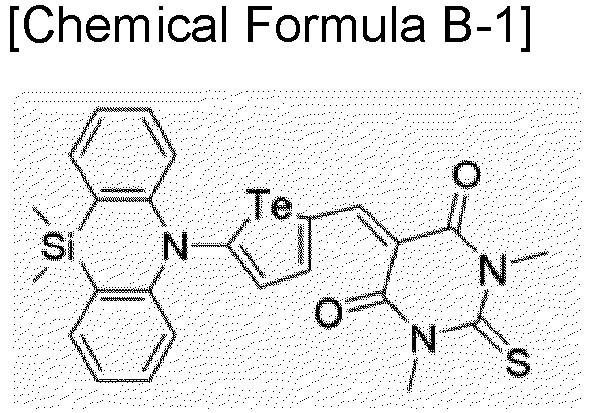
- A photoelectric conversion device is manufactured according to the same method as Example 1 except that the inorganic nanolayer is not formed.
- A photoelectric conversion device is manufactured according to the same method as Example 1 except that the p-type semiconductor and the n-type semiconductor are codeposited in a volume ratio of 1.2:1 to form a 90 nm-thick photoelectric conversion layer.
- A photoelectric conversion device is manufactured according to the same method as Example 2 except that the inorganic nanolayer is not formed.
- A photoelectric conversion device is manufactured according to the same method as Example 1 except that the p-type semiconductor and the n-type semiconductor are codeposited in a volume ratio of 2.5:1 to form an 80 nm-thick photoelectric conversion layer.
- A photoelectric conversion device is manufactured according to the same method as Example 3 except that the inorganic nanolayer is not formed.
- Remaining electrons characteristics of the photoelectric conversion devices of Examples and Comparative Examples are evaluated.
- The remaining electrons characteristics indicate an amount of charges photoelectrically-converted in one frame but not signal-treated and remain and thus read in the next frame and are evaluated by irradiating light in a wavelength spectrum of light in which a photoelectric conversion occurs into the photoelectric conversion devices according to Examples and Comparative Examples for a particular (or, alternatively, predetermined) time and then, turning the light off, and measuring a current amount per a 10-6 second unit using a Keithley 2400 equipment.
The results are shown in Tables 1 to 3.(Table 1) Remaining electrons (e-) 30 fps 240 fps 960 fps Example 1 1.3±0.1 10.3±1.0 18.0±1.8 Comparative Example 1 2.6±0.2 17.2±2.0 36.1±1.8 (Table 2) Remaining electrons (e-) 30 fps 240 fps 960 fps Example 2 2.7±0.1 17.0±1.2 40.2±1.5 Comparative Example 2 3.5±0.2 19.9±2.3 51.9±4.5 (Table 3) Remaining electrons (e-) 30 fps 240 fps 960 fps Example 3 13.7±0.2 104.8±1.7 251.1±3.3 Comparative Example 3 26.4±1.4 167.6±2.1 356.9±5.3 - Referring to Tables 1 to 3, the photoelectric conversion devices including the inorganic nanolayer according to Examples show improved remaining electrons characteristics compared with the photoelectric conversion devices including no inorganic nanolayer according to Comparative Examples.
- Photoelectric conversion efficiency of the photoelectric conversion devices according to Examples and Comparative Examples is evaluated.
- The photoelectric conversion efficiency (EQE) is evaluated in a wavelength spectrum of light of 400 nm to 720 nm in an Incident Photon to Current Efficiency (IPCE) method.
The results are shown in Tables 4 and 5.(Table 4) Photoelectric conversion efficiency (EQE, %) Example 1 72.3 Comparative Example 1 70.7 (Table 5) Photoelectric conversion efficiency (EQE, %) Example 3 61.3 Comparative Example 3 60.0 - Referring to Tables 4 and 5, the photoelectric conversion devices according to Examples show equivalent or improved photoelectric conversion efficiency compared with the photoelectric conversion devices according to Comparative Examples.
- An image sensor is designed by respectively applying the photoelectric conversion devices according to Examples and Comparative Examples, and YSNR10 of the organic CMOS image sensor is evaluated.
- The YSNR10 of the organic CMOS image sensor is a luminance (unit: lux) in which a ratio of signal to noise (signal/noise) becomes 10, wherein the signal is a signal sensitivity obtained by performing a RGB raw signal calculated by a FDTD (finite difference time domain method) with a color correction step through a color correction matrix (CCM), and the noise is a noise generated when measuring the signal in the organic CMOS image sensor. The color correction step is a step of reducing a difference from the real color by image-processing the RGB raw signal obtained from the organic CMOS image sensor. As the YSNR10 has the lower value, the image characteristics are getting the better at a low luminance.
- The results are shown in Table 6.
(Table 6) YSNR10 Example 1 84 Comparative Example 1 87 - Referring to Table 6, YSNR10 of the photoelectric conversion device according to Example is lower than that of the photoelectric conversion device according to Comparative Example, and thus it may be expected that the sensitivity of the organic CMOS image sensor may be improved.
Claims (15)
- A photoelectric conversion device (90, 90-1, 90-2, 90-3, 91, 100, 100a, 100b, 100c, 200), comprising:a first electrode (10, 10a, 10b, 10c) and a second electrode (20, 20a, 20b, 20c) facing each other;a photoelectric conversion layer (30, 30a, 30b, 30c) between the first electrode (10, 10a, 10b, 10c) and the second electrode (20, 20a, 20b, 20c), the photoelectric conversion layer (30, 30a, 30b, 30c) configured to absorb light in at least one part of a wavelength spectrum of light and to convert the absorbed light into an electric signal; andan inorganic nanolayer (40, 40a, 40b, 40c) having a thickness equal to or less than 5 nanometers (nm) between the first electrode (10, 10a, 10b, 10c) and the photoelectric conversion layer (30, 30a, 30b, 30c),whereinone surface of the inorganic nanolayer (40, 40a, 40b, 40c) is in contact with the first electrode (10, 10a, 10b, 10c), andanother, opposite surface of the inorganic nanolayer (40, 40a, 40b, 40c) is in contact with the photoelectric conversion layer (30, 30a, 30b, 30c),characterized in that the inorganic nanolayer (40, 40a, 40b, 40c) includes a lanthanide element, and the lanthanide element is ytterbium (Yb).
- The photoelectric conversion device (90, 90-1, 90-2, 90-3, 91, 100, 100a, 100b, 100c, 200) of claim 1, wherein the first electrode (10, 10a, 10b, 10c) includesa transparent electrode having a light transmittance of greater than or equal to 80 %, ora reflective electrode having a light transmittance of less than 10 %.
- The photoelectric conversion device (90, 90-1, 90-2, 90-3, 91, 100, 100a, 100b, 100c, 200) of claim 2, wherein the first electrode (10, 10a, 10b, 10c) includes the transparent electrode, and the transparent electrode includes at least one of an oxide conductor and a carbon conductor.
- The photoelectric conversion device (90, 90-1, 90-2, 90-3, 91, 100, 100a, 100b, 100c, 200) of any of claims 1-3, wherein the thickness of the inorganic nanolayer (40, 40a, 40b, 40c) is less than or equal to 2 nm.
- The photoelectric conversion device (90, 90-1, 90-2, 90-3, 91, 100, 100a, 100b, 100c, 200) of any of claims 1-4, wherein the first electrode (10, 10a, 10b, 10c) is a cathode and the second electrode is an anode.
- The photoelectric conversion device of any of claims 1-5,wherein the first electrode (10, 10a, 10b, 10c), includes a conductor, andwherein the effective work function at the surface of the first electrode (10, 10a, 10b, 10c) facing the photoelectric conversion layer (30, 30a, 30b, 30c) is less than the work function of the conductor.
- The photoelectric conversion device (90, 90-1, 90-2, 90-3, 91, 100, 100a, 100b, 100c, 200) of claim 6, wherein a difference between the work function of the conductor and the effective work function at the surface of the first electrode (10, 10a, 10b, 10c) facing the photoelectric conversion layer (30, 30a, 30b, 30c) is greater than or equal to 0.5 eV.
- The photoelectric conversion device (90, 90-1, 90-2, 90-3, 91, 100, 100a, 100b, 100c, 200) of claims 6 or 7, whereinthe work function of the conductor is greater than or equal to 4.5 eV, andthe effective work function at the surface of the first electrode (10, 10a, 10b, 10c) facing the photoelectric conversion layer (30, 30a, 30b, 30c) is less than or equal to 4.0 eV.
- The photoelectric conversion device (90, 90-1, 90-2, 90-3, 91, 100, 100a, 100b, 100c, 200) of claim 8, wherein the effective work function at the surface of the first electrode (10, 10a, 10b, 10c) facing the photoelectric conversion layer (30, 30a, 30b, 30c) is less than or equal to 3.0 eV.
- The photoelectric conversion device (90, 90-1, 90-2, 90-3, 91, 100, 100a, 100b, 100c, 200) of any of claims 6-9, wherein the transparent conductor includes an oxide conductor or a carbon conductor.
- The photoelectric conversion device (90, 90-1, 90-2, 90-3, 91, 100, 100a, 100b, 100c, 200) of any of claims 6-10, wherein the inorganic nanolayer (40, 40a, 40b, 40c) has a thickness of less than or equal to 2 nm.
- The photoelectric conversion device (90, 90-1, 90-2, 90-3, 91, 100, 100a, 100b, 100c, 200) of any of claims 6-11, wherein the first electrode (10, 10a, 10b, 10c) is a cathode and the second electrode (20, 20a, 20b, 20c) is an anode.
- An electronic device (1700) comprising the photoelectric conversion device (90, 90-1, 90-2, 90-3, 91, 100, 100a, 100b, 100c, 200) of any of claims 1-12.
- An organic sensor (400, 500, 600, 700, 800, 900, 1000, 1100, 1200, 1300, 1740) comprising the photoelectric conversion device (90, 90-1, 90-2, 90-3, 91, 100, 100a, 100b, 100c, 200) of any of claims 1-12.
- An electronic device (1700) comprising the organic sensor (400, 500, 600, 700, 800, 900, 1000, 1100, 1200, 1300, 1740) of claim 14.
Applications Claiming Priority (1)
| Application Number | Priority Date | Filing Date | Title |
|---|---|---|---|
| KR20180139824 | 2018-11-14 |
Publications (2)
| Publication Number | Publication Date |
|---|---|
| EP3654397A1 EP3654397A1 (en) | 2020-05-20 |
| EP3654397B1 true EP3654397B1 (en) | 2025-04-16 |
Family
ID=68109189
Family Applications (1)
| Application Number | Title | Priority Date | Filing Date |
|---|---|---|---|
| EP19200760.7A Active EP3654397B1 (en) | 2018-11-14 | 2019-10-01 | Photoelectric conversion devices and organic sensors and electronic devices |
Country Status (4)
| Country | Link |
|---|---|
| US (2) | US10886336B2 (en) |
| EP (1) | EP3654397B1 (en) |
| KR (1) | KR102790192B1 (en) |
| CN (1) | CN111192961A (en) |
Families Citing this family (4)
| Publication number | Priority date | Publication date | Assignee | Title |
|---|---|---|---|---|
| US12009379B2 (en) * | 2017-05-01 | 2024-06-11 | Visera Technologies Company Limited | Image sensor |
| US12439707B2 (en) | 2021-06-28 | 2025-10-07 | Samsung Electronics Co., Ltd. | Infrared photodiode and sensor and electronic device |
| US12048172B2 (en) | 2021-09-03 | 2024-07-23 | Visera Technologies Company Limited | Solid-state image sensor |
| CN114823722B (en) | 2022-04-07 | 2025-06-03 | 武汉华星光电半导体显示技术有限公司 | Display Panel |
Family Cites Families (12)
| Publication number | Priority date | Publication date | Assignee | Title |
|---|---|---|---|---|
| JP2004207142A (en) * | 2002-12-26 | 2004-07-22 | Seiko Epson Corp | Method of manufacturing organic electroluminescence device, organic electroluminescence device, electronic equipment |
| JP2007081137A (en) * | 2005-09-14 | 2007-03-29 | Fujifilm Corp | Photoelectric conversion device and solid-state imaging device |
| JP4893767B2 (en) | 2009-03-24 | 2012-03-07 | 富士ゼロックス株式会社 | Organic semiconductor transistor |
| EP2452946B1 (en) | 2010-11-16 | 2014-05-07 | Novaled AG | Pyridylphosphinoxides for organic electronic device and organic electronic device |
| US9379343B2 (en) | 2012-09-10 | 2016-06-28 | Samsung Electronics Co., Ltd. | Light transmissive electrode, organic photoelectric device, and image sensor |
| KR101920848B1 (en) | 2012-09-13 | 2018-11-22 | 삼성전자주식회사 | Organic photoelectronic device and image sensor |
| JP6049556B2 (en) | 2013-07-01 | 2016-12-21 | 株式会社東芝 | SOLAR CELL, SOLAR CELL MODULE, AND SOLAR CELL MANUFACTURING METHOD |
| JP2016058455A (en) | 2014-09-05 | 2016-04-21 | 株式会社東芝 | Photoelectric conversion element, wiring board for photoelectric conversion element, manufacturing method of photoelectric conversion element, and photoelectric conversion structure |
| JP2016076567A (en) * | 2014-10-06 | 2016-05-12 | ソニー株式会社 | Imaging apparatus, manufacturing apparatus, and manufacturing method |
| US20160111473A1 (en) | 2014-10-17 | 2016-04-21 | General Electric Company | Organic photodiodes, organic x-ray detectors and x-ray systems |
| KR101655012B1 (en) * | 2015-02-02 | 2016-09-22 | 서강대학교산학협력단 | Transparent organic photovoltaic cell for smart window comprising ytterbium and buffer layer |
| WO2016185858A1 (en) * | 2015-05-19 | 2016-11-24 | ソニー株式会社 | Imaging element, multilayer imaging element and imaging device |
-
2019
- 2019-07-29 US US16/524,626 patent/US10886336B2/en active Active
- 2019-10-01 EP EP19200760.7A patent/EP3654397B1/en active Active
- 2019-10-01 KR KR1020190121679A patent/KR102790192B1/en active Active
- 2019-10-24 CN CN201911017125.4A patent/CN111192961A/en active Pending
-
2020
- 2020-12-21 US US17/128,782 patent/US11437438B2/en active Active
Also Published As
| Publication number | Publication date |
|---|---|
| CN111192961A (en) | 2020-05-22 |
| US20210118956A1 (en) | 2021-04-22 |
| US11437438B2 (en) | 2022-09-06 |
| EP3654397A1 (en) | 2020-05-20 |
| US20200152703A1 (en) | 2020-05-14 |
| US10886336B2 (en) | 2021-01-05 |
| KR102790192B1 (en) | 2025-04-04 |
| KR20200056286A (en) | 2020-05-22 |
Similar Documents
| Publication | Publication Date | Title |
|---|---|---|
| EP3509108B1 (en) | Photoelectric devices and image sensors and electronic devices | |
| EP3493262B1 (en) | Photoelectric devices and image sensors and electronic devices | |
| US11437438B2 (en) | Photoelectric conversion devices and organic sensors and electronic devices | |
| EP3696857A1 (en) | Photoelectric diodes and organic sensors and electronic devices | |
| US20230354705A1 (en) | Photoelectric conversion device and sensor and electronic device | |
| EP3993052B1 (en) | Sensor and electronic device | |
| US11855236B2 (en) | Sensors and electronic devices | |
| US11591347B2 (en) | Compounds and films and photoelectric diodes and organic sensors and electronic devices | |
| US11631819B2 (en) | Photoelectric conversion device, organic sensor and electronic device | |
| EP3739642B1 (en) | Photoelectric conversion devices and organic sensors and electronic devices | |
| US11557741B2 (en) | Photoelectric conversion devices and organic sensors and electronic devices | |
| KR102819096B1 (en) | Photoelectric device and sensor and electronic device | |
| US11839096B2 (en) | Organic sensors and electronic devices | |
| US12114567B2 (en) | Photoelectric devices having charge transport layer including first charge transport material and second charge transport material and sensors and electronic devices | |
| EP3660935A1 (en) | Photoelectric conversion devices and organic sensors and electronic devices | |
| JP7445411B2 (en) | Photoelectric conversion element and organic sensor and electronic device including the same |
Legal Events
| Date | Code | Title | Description |
|---|---|---|---|
| PUAI | Public reference made under article 153(3) epc to a published international application that has entered the european phase |
Free format text: ORIGINAL CODE: 0009012 |
|
| STAA | Information on the status of an ep patent application or granted ep patent |
Free format text: STATUS: THE APPLICATION HAS BEEN PUBLISHED |
|
| AK | Designated contracting states |
Kind code of ref document: A1 Designated state(s): AL AT BE BG CH CY CZ DE DK EE ES FI FR GB GR HR HU IE IS IT LI LT LU LV MC MK MT NL NO PL PT RO RS SE SI SK SM TR |
|
| AX | Request for extension of the european patent |
Extension state: BA ME |
|
| STAA | Information on the status of an ep patent application or granted ep patent |
Free format text: STATUS: REQUEST FOR EXAMINATION WAS MADE |
|
| 17P | Request for examination filed |
Effective date: 20201022 |
|
| RBV | Designated contracting states (corrected) |
Designated state(s): AL AT BE BG CH CY CZ DE DK EE ES FI FR GB GR HR HU IE IS IT LI LT LU LV MC MK MT NL NO PL PT RO RS SE SI SK SM TR |
|
| STAA | Information on the status of an ep patent application or granted ep patent |
Free format text: STATUS: EXAMINATION IS IN PROGRESS |
|
| 17Q | First examination report despatched |
Effective date: 20220208 |
|
| P01 | Opt-out of the competence of the unified patent court (upc) registered |
Effective date: 20230519 |
|
| REG | Reference to a national code |
Ref country code: DE Ref legal event code: R079 Ipc: H10K0030820000 Ref country code: DE Ref legal event code: R079 Ref document number: 602019068637 Country of ref document: DE Free format text: PREVIOUS MAIN CLASS: H01L0051440000 Ipc: H10K0030820000 |
|
| GRAP | Despatch of communication of intention to grant a patent |
Free format text: ORIGINAL CODE: EPIDOSNIGR1 |
|
| STAA | Information on the status of an ep patent application or granted ep patent |
Free format text: STATUS: GRANT OF PATENT IS INTENDED |
|
| RIC1 | Information provided on ipc code assigned before grant |
Ipc: H10K 30/83 20230101ALI20240816BHEP Ipc: H10K 30/82 20230101AFI20240816BHEP |
|
| INTG | Intention to grant announced |
Effective date: 20240902 |
|
| GRAJ | Information related to disapproval of communication of intention to grant by the applicant or resumption of examination proceedings by the epo deleted |
Free format text: ORIGINAL CODE: EPIDOSDIGR1 |
|
| STAA | Information on the status of an ep patent application or granted ep patent |
Free format text: STATUS: EXAMINATION IS IN PROGRESS |
|
| GRAP | Despatch of communication of intention to grant a patent |
Free format text: ORIGINAL CODE: EPIDOSNIGR1 |
|
| STAA | Information on the status of an ep patent application or granted ep patent |
Free format text: STATUS: GRANT OF PATENT IS INTENDED |
|
| INTC | Intention to grant announced (deleted) | ||
| INTG | Intention to grant announced |
Effective date: 20241120 |
|
| GRAS | Grant fee paid |
Free format text: ORIGINAL CODE: EPIDOSNIGR3 |
|
| GRAA | (expected) grant |
Free format text: ORIGINAL CODE: 0009210 |
|
| STAA | Information on the status of an ep patent application or granted ep patent |
Free format text: STATUS: THE PATENT HAS BEEN GRANTED |
|
| AK | Designated contracting states |
Kind code of ref document: B1 Designated state(s): AL AT BE BG CH CY CZ DE DK EE ES FI FR GB GR HR HU IE IS IT LI LT LU LV MC MK MT NL NO PL PT RO RS SE SI SK SM TR |
|
| REG | Reference to a national code |
Ref country code: GB Ref legal event code: FG4D |
|
| REG | Reference to a national code |
Ref country code: CH Ref legal event code: EP |
|
| REG | Reference to a national code |
Ref country code: IE Ref legal event code: FG4D |
|
| REG | Reference to a national code |
Ref country code: DE Ref legal event code: R096 Ref document number: 602019068637 Country of ref document: DE |
|
| REG | Reference to a national code |
Ref country code: NL Ref legal event code: MP Effective date: 20250416 |
|
| PG25 | Lapsed in a contracting state [announced via postgrant information from national office to epo] |
Ref country code: NL Free format text: LAPSE BECAUSE OF FAILURE TO SUBMIT A TRANSLATION OF THE DESCRIPTION OR TO PAY THE FEE WITHIN THE PRESCRIBED TIME-LIMIT Effective date: 20250416 |
|
| REG | Reference to a national code |
Ref country code: AT Ref legal event code: MK05 Ref document number: 1786789 Country of ref document: AT Kind code of ref document: T Effective date: 20250416 |
|
| PG25 | Lapsed in a contracting state [announced via postgrant information from national office to epo] |
Ref country code: PT Free format text: LAPSE BECAUSE OF FAILURE TO SUBMIT A TRANSLATION OF THE DESCRIPTION OR TO PAY THE FEE WITHIN THE PRESCRIBED TIME-LIMIT Effective date: 20250818 Ref country code: FI Free format text: LAPSE BECAUSE OF FAILURE TO SUBMIT A TRANSLATION OF THE DESCRIPTION OR TO PAY THE FEE WITHIN THE PRESCRIBED TIME-LIMIT Effective date: 20250416 Ref country code: ES Free format text: LAPSE BECAUSE OF FAILURE TO SUBMIT A TRANSLATION OF THE DESCRIPTION OR TO PAY THE FEE WITHIN THE PRESCRIBED TIME-LIMIT Effective date: 20250416 |
|
| REG | Reference to a national code |
Ref country code: LT Ref legal event code: MG9D |
|
| PG25 | Lapsed in a contracting state [announced via postgrant information from national office to epo] |
Ref country code: GR Free format text: LAPSE BECAUSE OF FAILURE TO SUBMIT A TRANSLATION OF THE DESCRIPTION OR TO PAY THE FEE WITHIN THE PRESCRIBED TIME-LIMIT Effective date: 20250717 Ref country code: NO Free format text: LAPSE BECAUSE OF FAILURE TO SUBMIT A TRANSLATION OF THE DESCRIPTION OR TO PAY THE FEE WITHIN THE PRESCRIBED TIME-LIMIT Effective date: 20250716 |
|
| PG25 | Lapsed in a contracting state [announced via postgrant information from national office to epo] |
Ref country code: PL Free format text: LAPSE BECAUSE OF FAILURE TO SUBMIT A TRANSLATION OF THE DESCRIPTION OR TO PAY THE FEE WITHIN THE PRESCRIBED TIME-LIMIT Effective date: 20250416 |
|
| PG25 | Lapsed in a contracting state [announced via postgrant information from national office to epo] |
Ref country code: BG Free format text: LAPSE BECAUSE OF FAILURE TO SUBMIT A TRANSLATION OF THE DESCRIPTION OR TO PAY THE FEE WITHIN THE PRESCRIBED TIME-LIMIT Effective date: 20250416 |
|
| PGFP | Annual fee paid to national office [announced via postgrant information from national office to epo] |
Ref country code: GB Payment date: 20250911 Year of fee payment: 7 |
|
| PG25 | Lapsed in a contracting state [announced via postgrant information from national office to epo] |
Ref country code: HR Free format text: LAPSE BECAUSE OF FAILURE TO SUBMIT A TRANSLATION OF THE DESCRIPTION OR TO PAY THE FEE WITHIN THE PRESCRIBED TIME-LIMIT Effective date: 20250416 |
|
| PG25 | Lapsed in a contracting state [announced via postgrant information from national office to epo] |
Ref country code: AT Free format text: LAPSE BECAUSE OF FAILURE TO SUBMIT A TRANSLATION OF THE DESCRIPTION OR TO PAY THE FEE WITHIN THE PRESCRIBED TIME-LIMIT Effective date: 20250416 |
|
| PGFP | Annual fee paid to national office [announced via postgrant information from national office to epo] |
Ref country code: FR Payment date: 20250908 Year of fee payment: 7 |
|
| PG25 | Lapsed in a contracting state [announced via postgrant information from national office to epo] |
Ref country code: RS Free format text: LAPSE BECAUSE OF FAILURE TO SUBMIT A TRANSLATION OF THE DESCRIPTION OR TO PAY THE FEE WITHIN THE PRESCRIBED TIME-LIMIT Effective date: 20250716 |
|
| PG25 | Lapsed in a contracting state [announced via postgrant information from national office to epo] |
Ref country code: IS Free format text: LAPSE BECAUSE OF FAILURE TO SUBMIT A TRANSLATION OF THE DESCRIPTION OR TO PAY THE FEE WITHIN THE PRESCRIBED TIME-LIMIT Effective date: 20250816 |
|
| PG25 | Lapsed in a contracting state [announced via postgrant information from national office to epo] |
Ref country code: LV Free format text: LAPSE BECAUSE OF FAILURE TO SUBMIT A TRANSLATION OF THE DESCRIPTION OR TO PAY THE FEE WITHIN THE PRESCRIBED TIME-LIMIT Effective date: 20250416 |
|
| PGFP | Annual fee paid to national office [announced via postgrant information from national office to epo] |
Ref country code: DE Payment date: 20250910 Year of fee payment: 7 |
|
| PG25 | Lapsed in a contracting state [announced via postgrant information from national office to epo] |
Ref country code: SM Free format text: LAPSE BECAUSE OF FAILURE TO SUBMIT A TRANSLATION OF THE DESCRIPTION OR TO PAY THE FEE WITHIN THE PRESCRIBED TIME-LIMIT Effective date: 20250416 Ref country code: DK Free format text: LAPSE BECAUSE OF FAILURE TO SUBMIT A TRANSLATION OF THE DESCRIPTION OR TO PAY THE FEE WITHIN THE PRESCRIBED TIME-LIMIT Effective date: 20250416 |
|
| PG25 | Lapsed in a contracting state [announced via postgrant information from national office to epo] |
Ref country code: CZ Free format text: LAPSE BECAUSE OF FAILURE TO SUBMIT A TRANSLATION OF THE DESCRIPTION OR TO PAY THE FEE WITHIN THE PRESCRIBED TIME-LIMIT Effective date: 20250416 |
|
| PG25 | Lapsed in a contracting state [announced via postgrant information from national office to epo] |
Ref country code: EE Free format text: LAPSE BECAUSE OF FAILURE TO SUBMIT A TRANSLATION OF THE DESCRIPTION OR TO PAY THE FEE WITHIN THE PRESCRIBED TIME-LIMIT Effective date: 20250416 |
|
| PG25 | Lapsed in a contracting state [announced via postgrant information from national office to epo] |
Ref country code: SK Free format text: LAPSE BECAUSE OF FAILURE TO SUBMIT A TRANSLATION OF THE DESCRIPTION OR TO PAY THE FEE WITHIN THE PRESCRIBED TIME-LIMIT Effective date: 20250416 Ref country code: RO Free format text: LAPSE BECAUSE OF FAILURE TO SUBMIT A TRANSLATION OF THE DESCRIPTION OR TO PAY THE FEE WITHIN THE PRESCRIBED TIME-LIMIT Effective date: 20250416 |
|
| PG25 | Lapsed in a contracting state [announced via postgrant information from national office to epo] |
Ref country code: IT Free format text: LAPSE BECAUSE OF FAILURE TO SUBMIT A TRANSLATION OF THE DESCRIPTION OR TO PAY THE FEE WITHIN THE PRESCRIBED TIME-LIMIT Effective date: 20250416 |