EP3654379B1 - Organic light emitting diode display device and method of driving the same - Google Patents
Organic light emitting diode display device and method of driving the same Download PDFInfo
- Publication number
- EP3654379B1 EP3654379B1 EP19207773.3A EP19207773A EP3654379B1 EP 3654379 B1 EP3654379 B1 EP 3654379B1 EP 19207773 A EP19207773 A EP 19207773A EP 3654379 B1 EP3654379 B1 EP 3654379B1
- Authority
- EP
- European Patent Office
- Prior art keywords
- pixels
- sub
- line
- lines
- horizontal pixel
- Prior art date
- Legal status (The legal status is an assumption and is not a legal conclusion. Google has not performed a legal analysis and makes no representation as to the accuracy of the status listed.)
- Active
Links
Images


Classifications
-
- G—PHYSICS
- G09—EDUCATION; CRYPTOGRAPHY; DISPLAY; ADVERTISING; SEALS
- G09G—ARRANGEMENTS OR CIRCUITS FOR CONTROL OF INDICATING DEVICES USING STATIC MEANS TO PRESENT VARIABLE INFORMATION
- G09G3/00—Control arrangements or circuits, of interest only in connection with visual indicators other than cathode-ray tubes
- G09G3/20—Control arrangements or circuits, of interest only in connection with visual indicators other than cathode-ray tubes for presentation of an assembly of a number of characters, e.g. a page, by composing the assembly by combination of individual elements arranged in a matrix no fixed position being assigned to or needed to be assigned to the individual characters or partial characters
- G09G3/22—Control arrangements or circuits, of interest only in connection with visual indicators other than cathode-ray tubes for presentation of an assembly of a number of characters, e.g. a page, by composing the assembly by combination of individual elements arranged in a matrix no fixed position being assigned to or needed to be assigned to the individual characters or partial characters using controlled light sources
- G09G3/30—Control arrangements or circuits, of interest only in connection with visual indicators other than cathode-ray tubes for presentation of an assembly of a number of characters, e.g. a page, by composing the assembly by combination of individual elements arranged in a matrix no fixed position being assigned to or needed to be assigned to the individual characters or partial characters using controlled light sources using electroluminescent panels
- G09G3/32—Control arrangements or circuits, of interest only in connection with visual indicators other than cathode-ray tubes for presentation of an assembly of a number of characters, e.g. a page, by composing the assembly by combination of individual elements arranged in a matrix no fixed position being assigned to or needed to be assigned to the individual characters or partial characters using controlled light sources using electroluminescent panels semiconductive, e.g. using light-emitting diodes [LED]
- G09G3/3208—Control arrangements or circuits, of interest only in connection with visual indicators other than cathode-ray tubes for presentation of an assembly of a number of characters, e.g. a page, by composing the assembly by combination of individual elements arranged in a matrix no fixed position being assigned to or needed to be assigned to the individual characters or partial characters using controlled light sources using electroluminescent panels semiconductive, e.g. using light-emitting diodes [LED] organic, e.g. using organic light-emitting diodes [OLED]
- G09G3/3225—Control arrangements or circuits, of interest only in connection with visual indicators other than cathode-ray tubes for presentation of an assembly of a number of characters, e.g. a page, by composing the assembly by combination of individual elements arranged in a matrix no fixed position being assigned to or needed to be assigned to the individual characters or partial characters using controlled light sources using electroluminescent panels semiconductive, e.g. using light-emitting diodes [LED] organic, e.g. using organic light-emitting diodes [OLED] using an active matrix
- G09G3/3258—Control arrangements or circuits, of interest only in connection with visual indicators other than cathode-ray tubes for presentation of an assembly of a number of characters, e.g. a page, by composing the assembly by combination of individual elements arranged in a matrix no fixed position being assigned to or needed to be assigned to the individual characters or partial characters using controlled light sources using electroluminescent panels semiconductive, e.g. using light-emitting diodes [LED] organic, e.g. using organic light-emitting diodes [OLED] using an active matrix with pixel circuitry controlling the voltage across the light-emitting element
-
- H—ELECTRICITY
- H10—SEMICONDUCTOR DEVICES; ELECTRIC SOLID-STATE DEVICES NOT OTHERWISE PROVIDED FOR
- H10K—ORGANIC ELECTRIC SOLID-STATE DEVICES
- H10K59/00—Integrated devices, or assemblies of multiple devices, comprising at least one organic light-emitting element covered by group H10K50/00
- H10K59/10—OLED displays
- H10K59/12—Active-matrix OLED [AMOLED] displays
- H10K59/131—Interconnections, e.g. wiring lines or terminals
-
- G—PHYSICS
- G09—EDUCATION; CRYPTOGRAPHY; DISPLAY; ADVERTISING; SEALS
- G09G—ARRANGEMENTS OR CIRCUITS FOR CONTROL OF INDICATING DEVICES USING STATIC MEANS TO PRESENT VARIABLE INFORMATION
- G09G3/00—Control arrangements or circuits, of interest only in connection with visual indicators other than cathode-ray tubes
- G09G3/20—Control arrangements or circuits, of interest only in connection with visual indicators other than cathode-ray tubes for presentation of an assembly of a number of characters, e.g. a page, by composing the assembly by combination of individual elements arranged in a matrix no fixed position being assigned to or needed to be assigned to the individual characters or partial characters
- G09G3/22—Control arrangements or circuits, of interest only in connection with visual indicators other than cathode-ray tubes for presentation of an assembly of a number of characters, e.g. a page, by composing the assembly by combination of individual elements arranged in a matrix no fixed position being assigned to or needed to be assigned to the individual characters or partial characters using controlled light sources
- G09G3/30—Control arrangements or circuits, of interest only in connection with visual indicators other than cathode-ray tubes for presentation of an assembly of a number of characters, e.g. a page, by composing the assembly by combination of individual elements arranged in a matrix no fixed position being assigned to or needed to be assigned to the individual characters or partial characters using controlled light sources using electroluminescent panels
- G09G3/32—Control arrangements or circuits, of interest only in connection with visual indicators other than cathode-ray tubes for presentation of an assembly of a number of characters, e.g. a page, by composing the assembly by combination of individual elements arranged in a matrix no fixed position being assigned to or needed to be assigned to the individual characters or partial characters using controlled light sources using electroluminescent panels semiconductive, e.g. using light-emitting diodes [LED]
- G09G3/3208—Control arrangements or circuits, of interest only in connection with visual indicators other than cathode-ray tubes for presentation of an assembly of a number of characters, e.g. a page, by composing the assembly by combination of individual elements arranged in a matrix no fixed position being assigned to or needed to be assigned to the individual characters or partial characters using controlled light sources using electroluminescent panels semiconductive, e.g. using light-emitting diodes [LED] organic, e.g. using organic light-emitting diodes [OLED]
- G09G3/3225—Control arrangements or circuits, of interest only in connection with visual indicators other than cathode-ray tubes for presentation of an assembly of a number of characters, e.g. a page, by composing the assembly by combination of individual elements arranged in a matrix no fixed position being assigned to or needed to be assigned to the individual characters or partial characters using controlled light sources using electroluminescent panels semiconductive, e.g. using light-emitting diodes [LED] organic, e.g. using organic light-emitting diodes [OLED] using an active matrix
- G09G3/3233—Control arrangements or circuits, of interest only in connection with visual indicators other than cathode-ray tubes for presentation of an assembly of a number of characters, e.g. a page, by composing the assembly by combination of individual elements arranged in a matrix no fixed position being assigned to or needed to be assigned to the individual characters or partial characters using controlled light sources using electroluminescent panels semiconductive, e.g. using light-emitting diodes [LED] organic, e.g. using organic light-emitting diodes [OLED] using an active matrix with pixel circuitry controlling the current through the light-emitting element
-
- H—ELECTRICITY
- H10—SEMICONDUCTOR DEVICES; ELECTRIC SOLID-STATE DEVICES NOT OTHERWISE PROVIDED FOR
- H10K—ORGANIC ELECTRIC SOLID-STATE DEVICES
- H10K59/00—Integrated devices, or assemblies of multiple devices, comprising at least one organic light-emitting element covered by group H10K50/00
- H10K59/10—OLED displays
- H10K59/12—Active-matrix OLED [AMOLED] displays
- H10K59/121—Active-matrix OLED [AMOLED] displays characterised by the geometry or disposition of pixel elements
-
- H—ELECTRICITY
- H10—SEMICONDUCTOR DEVICES; ELECTRIC SOLID-STATE DEVICES NOT OTHERWISE PROVIDED FOR
- H10K—ORGANIC ELECTRIC SOLID-STATE DEVICES
- H10K59/00—Integrated devices, or assemblies of multiple devices, comprising at least one organic light-emitting element covered by group H10K50/00
- H10K59/10—OLED displays
- H10K59/12—Active-matrix OLED [AMOLED] displays
- H10K59/121—Active-matrix OLED [AMOLED] displays characterised by the geometry or disposition of pixel elements
- H10K59/1213—Active-matrix OLED [AMOLED] displays characterised by the geometry or disposition of pixel elements the pixel elements being TFTs
-
- H—ELECTRICITY
- H10—SEMICONDUCTOR DEVICES; ELECTRIC SOLID-STATE DEVICES NOT OTHERWISE PROVIDED FOR
- H10K—ORGANIC ELECTRIC SOLID-STATE DEVICES
- H10K59/00—Integrated devices, or assemblies of multiple devices, comprising at least one organic light-emitting element covered by group H10K50/00
- H10K59/10—OLED displays
- H10K59/12—Active-matrix OLED [AMOLED] displays
- H10K59/121—Active-matrix OLED [AMOLED] displays characterised by the geometry or disposition of pixel elements
- H10K59/1216—Active-matrix OLED [AMOLED] displays characterised by the geometry or disposition of pixel elements the pixel elements being capacitors
-
- H—ELECTRICITY
- H10—SEMICONDUCTOR DEVICES; ELECTRIC SOLID-STATE DEVICES NOT OTHERWISE PROVIDED FOR
- H10K—ORGANIC ELECTRIC SOLID-STATE DEVICES
- H10K59/00—Integrated devices, or assemblies of multiple devices, comprising at least one organic light-emitting element covered by group H10K50/00
- H10K59/10—OLED displays
- H10K59/12—Active-matrix OLED [AMOLED] displays
- H10K59/123—Connection of the pixel electrodes to the thin film transistors [TFT]
-
- H—ELECTRICITY
- H10—SEMICONDUCTOR DEVICES; ELECTRIC SOLID-STATE DEVICES NOT OTHERWISE PROVIDED FOR
- H10K—ORGANIC ELECTRIC SOLID-STATE DEVICES
- H10K59/00—Integrated devices, or assemblies of multiple devices, comprising at least one organic light-emitting element covered by group H10K50/00
- H10K59/30—Devices specially adapted for multicolour light emission
- H10K59/35—Devices specially adapted for multicolour light emission comprising red-green-blue [RGB] subpixels
- H10K59/351—Devices specially adapted for multicolour light emission comprising red-green-blue [RGB] subpixels comprising more than three subpixels, e.g. red-green-blue-white [RGBW]
-
- G—PHYSICS
- G09—EDUCATION; CRYPTOGRAPHY; DISPLAY; ADVERTISING; SEALS
- G09G—ARRANGEMENTS OR CIRCUITS FOR CONTROL OF INDICATING DEVICES USING STATIC MEANS TO PRESENT VARIABLE INFORMATION
- G09G2300/00—Aspects of the constitution of display devices
- G09G2300/04—Structural and physical details of display devices
- G09G2300/0421—Structural details of the set of electrodes
- G09G2300/0426—Layout of electrodes and connections
-
- G—PHYSICS
- G09—EDUCATION; CRYPTOGRAPHY; DISPLAY; ADVERTISING; SEALS
- G09G—ARRANGEMENTS OR CIRCUITS FOR CONTROL OF INDICATING DEVICES USING STATIC MEANS TO PRESENT VARIABLE INFORMATION
- G09G2300/00—Aspects of the constitution of display devices
- G09G2300/08—Active matrix structure, i.e. with use of active elements, inclusive of non-linear two terminal elements, in the pixels together with light emitting or modulating elements
- G09G2300/0809—Several active elements per pixel in active matrix panels
- G09G2300/0819—Several active elements per pixel in active matrix panels used for counteracting undesired variations, e.g. feedback or autozeroing
-
- G—PHYSICS
- G09—EDUCATION; CRYPTOGRAPHY; DISPLAY; ADVERTISING; SEALS
- G09G—ARRANGEMENTS OR CIRCUITS FOR CONTROL OF INDICATING DEVICES USING STATIC MEANS TO PRESENT VARIABLE INFORMATION
- G09G2310/00—Command of the display device
- G09G2310/02—Addressing, scanning or driving the display screen or processing steps related thereto
- G09G2310/0202—Addressing of scan or signal lines
- G09G2310/0205—Simultaneous scanning of several lines in flat panels
- G09G2310/021—Double addressing, i.e. scanning two or more lines, e.g. lines 2 and 3; 4 and 5, at a time in a first field, followed by scanning two or more lines in another combination, e.g. lines 1 and 2; 3 and 4, in a second field
-
- G—PHYSICS
- G09—EDUCATION; CRYPTOGRAPHY; DISPLAY; ADVERTISING; SEALS
- G09G—ARRANGEMENTS OR CIRCUITS FOR CONTROL OF INDICATING DEVICES USING STATIC MEANS TO PRESENT VARIABLE INFORMATION
- G09G2310/00—Command of the display device
- G09G2310/02—Addressing, scanning or driving the display screen or processing steps related thereto
- G09G2310/0243—Details of the generation of driving signals
- G09G2310/0251—Precharge or discharge of pixel before applying new pixel voltage
-
- G—PHYSICS
- G09—EDUCATION; CRYPTOGRAPHY; DISPLAY; ADVERTISING; SEALS
- G09G—ARRANGEMENTS OR CIRCUITS FOR CONTROL OF INDICATING DEVICES USING STATIC MEANS TO PRESENT VARIABLE INFORMATION
- G09G2310/00—Command of the display device
- G09G2310/06—Details of flat display driving waveforms
- G09G2310/061—Details of flat display driving waveforms for resetting or blanking
-
- G—PHYSICS
- G09—EDUCATION; CRYPTOGRAPHY; DISPLAY; ADVERTISING; SEALS
- G09G—ARRANGEMENTS OR CIRCUITS FOR CONTROL OF INDICATING DEVICES USING STATIC MEANS TO PRESENT VARIABLE INFORMATION
- G09G2310/00—Command of the display device
- G09G2310/06—Details of flat display driving waveforms
- G09G2310/067—Special waveforms for scanning, where no circuit details of the gate driver are given
-
- G—PHYSICS
- G09—EDUCATION; CRYPTOGRAPHY; DISPLAY; ADVERTISING; SEALS
- G09G—ARRANGEMENTS OR CIRCUITS FOR CONTROL OF INDICATING DEVICES USING STATIC MEANS TO PRESENT VARIABLE INFORMATION
- G09G2320/00—Control of display operating conditions
- G09G2320/02—Improving the quality of display appearance
- G09G2320/0233—Improving the luminance or brightness uniformity across the screen
-
- G—PHYSICS
- G09—EDUCATION; CRYPTOGRAPHY; DISPLAY; ADVERTISING; SEALS
- G09G—ARRANGEMENTS OR CIRCUITS FOR CONTROL OF INDICATING DEVICES USING STATIC MEANS TO PRESENT VARIABLE INFORMATION
- G09G2320/00—Control of display operating conditions
- G09G2320/02—Improving the quality of display appearance
- G09G2320/029—Improving the quality of display appearance by monitoring one or more pixels in the display panel, e.g. by monitoring a fixed reference pixel
- G09G2320/0295—Improving the quality of display appearance by monitoring one or more pixels in the display panel, e.g. by monitoring a fixed reference pixel by monitoring each display pixel
-
- H—ELECTRICITY
- H10—SEMICONDUCTOR DEVICES; ELECTRIC SOLID-STATE DEVICES NOT OTHERWISE PROVIDED FOR
- H10D—INORGANIC ELECTRIC SEMICONDUCTOR DEVICES
- H10D86/00—Integrated devices formed in or on insulating or conducting substrates, e.g. formed in silicon-on-insulator [SOI] substrates or on stainless steel or glass substrates
- H10D86/40—Integrated devices formed in or on insulating or conducting substrates, e.g. formed in silicon-on-insulator [SOI] substrates or on stainless steel or glass substrates characterised by multiple TFTs
- H10D86/441—Interconnections, e.g. scanning lines
-
- H—ELECTRICITY
- H10—SEMICONDUCTOR DEVICES; ELECTRIC SOLID-STATE DEVICES NOT OTHERWISE PROVIDED FOR
- H10D—INORGANIC ELECTRIC SEMICONDUCTOR DEVICES
- H10D86/00—Integrated devices formed in or on insulating or conducting substrates, e.g. formed in silicon-on-insulator [SOI] substrates or on stainless steel or glass substrates
- H10D86/40—Integrated devices formed in or on insulating or conducting substrates, e.g. formed in silicon-on-insulator [SOI] substrates or on stainless steel or glass substrates characterised by multiple TFTs
- H10D86/481—Integrated devices formed in or on insulating or conducting substrates, e.g. formed in silicon-on-insulator [SOI] substrates or on stainless steel or glass substrates characterised by multiple TFTs integrated with passive devices, e.g. auxiliary capacitors
-
- H—ELECTRICITY
- H10—SEMICONDUCTOR DEVICES; ELECTRIC SOLID-STATE DEVICES NOT OTHERWISE PROVIDED FOR
- H10D—INORGANIC ELECTRIC SEMICONDUCTOR DEVICES
- H10D86/00—Integrated devices formed in or on insulating or conducting substrates, e.g. formed in silicon-on-insulator [SOI] substrates or on stainless steel or glass substrates
- H10D86/40—Integrated devices formed in or on insulating or conducting substrates, e.g. formed in silicon-on-insulator [SOI] substrates or on stainless steel or glass substrates characterised by multiple TFTs
- H10D86/60—Integrated devices formed in or on insulating or conducting substrates, e.g. formed in silicon-on-insulator [SOI] substrates or on stainless steel or glass substrates characterised by multiple TFTs wherein the TFTs are in active matrices
Definitions
- the present disclosure relates to a display device, and more particularly, to an organic light emitting diode display device where deterioration such as a horizontal bright line is prevented by supplying a reference voltage to adjacent horizontal pixel lines through different reference lines and a method of driving the organic light emitting diode display device.
- an organic light emitting diode (OLED) display device has a relatively high luminance and a relatively low driving voltage.
- the OLED display device Since the OLED display device has an emissive type, the OLED display device has a relatively great contrast ratio. In addition, since the OLED display device has a response time of several microseconds, the OLED display device has an advantage in displaying a moving image. The OLED display device also has a relatively wide viewing angle and is stable even under a relatively low temperature. Since the OLED display device is driven by a relatively low voltage of direct current (DC) 5V to 15V, a driving circuit can be easily designed and manufactured.
- DC direct current
- the OLED display device is fabricated through a deposition and an encapsulation, the OLED display device has a simplified fabrication process.
- a plurality of thin film transistors such as a switching TFT, a driving TFT and a sensing TFT, a storage capacitor and a light emitting diode may be formed in each pixel of the OLED display device.
- the sensing TFT is connected to the driving TFT and a reference line to initialize a source electrode of the driving TFT by applying a reference voltage to the source electrode.
- a threshold voltage of the driving TFT stored in the storage capacitor is reflected to a data signal such that a variation in the threshold voltage of the driving TFT is compensated.
- the reference voltage is supplied to all the horizontal pixel lines of the OLED display device through a single reference line.
- the sensing TFT of an (n)th horizontal pixel line is turned on to initialize the source electrode of the driving TFT
- the sensing TFT of an (n+1)th horizontal pixel line is also turned on.
- a current is instantaneously generated in the single reference line supplying the reference voltage to the (n)th and (n+1)th horizontal pixel lines, and a voltage of pthe source electrode of the driving TFT of the (n)th horizontal pixel line instantaneously increases to have an inflection point where a rate of change varies.
- the inflection point of the voltage of the source electrode of the driving TFT may influence a turn-on current of the driving TFT.
- a uniform turn-on current is generated in the driving TFT in all the horizontal pixel lines and an image displayed by the OLED display device has no deterioration.
- a technology that a response speed of an image is improved by inserting a black data into an image data has been developed.
- the turn-on sections of the switching TFT and the sensing TFT do not overlap each other and are separated from each other for inserting the black data.
- the voltage of the source electrode of the driving TFT in the horizontal pixel lines where the turn-on sectons overlap each other and the voltage of the source electrode of the driving TFT in the horizontal pixel lines where the turn-on sections do not overlap each other have different inflection points according to overlap.
- the inflection point of the voltage of the source electrode of the driving TFT in the (n)th horizontal pixel line influenced by the (n+1)th horizontal pixel line becomes different from the inflection point of the voltage of the source electrode of the driving TFT in the (n+1)th horizontal pixel line influenced by the (n+2)th horizontal pixel line.
- the turn-on current becomes non-uniform due to the difference of the inflection points of the voltages of the source electrodes of the driving TFTs and deterioration such as a horizontal bright line occurs in an image displayed by the OLED display device. As a result, a display quality of the OLED display device is deteriorated.
- US 2015/129853 A1 discloses an organic light emitting diode display device including a substrate including a display and non-display regions at a periphery of the display region with red, green, blue and white pixel regions as one pixel group formed in the display region and the display region divided into a first region and a second region; an organic light emitting diode in each of the red, green, blue and white pixel region; first to third power lines respectively disposed at an end of the first region, at an opposite end of the second region and a boundary of the first and second regions and connected to the organic light emitting diode; a first drive integrated circuit connected to the first and third power lines; and a second drive integrated circuit connected to the second and third power lines, wherein the first and second regions are symmetric with respect to the third power line.
- US 2017/157579 A1 discloses an organic light emitting display panel including an active area corresponding to an image display region, and a non-active area corresponding to a region outside of the active area, wherein the active area includes a plurality of signal lines arranged in an array, wherein the non-active area includes a pad region to which a source driver IC is mounted, and a switching structure, wherein the pad region includes a plurality of pads arranged in correspondence with the array of the signal lines, and wherein the switching structure includes: a common reference voltage pad-connection terminal connected to a common reference voltage pad of the display panel; a plurality of reference voltage line-connection terminals connected to a plurality of reference voltage lines of the display panel; and a switching circuit to switch connections between a common reference voltage pad-connection terminal and the plurality of reference voltage line-connection terminals.
- US 2015/062192 A1 discloses an organic light emitting display device including a plurality of pixels configured to each include an organic light emitting device and a pixel circuit that includes a driving transistor which supplies the data current, which is based on a difference voltage between a data voltage and a reference voltage, to the organic light emitting device, a plurality of data lines configured to respectively supply a plurality of the data voltages to the plurality of pixels, a plurality of gate lines configured to supply a gate signal to the pixels, and a plurality of reference lines connected to at least one of the pixels, and configured to supply the reference voltage to the connected pixel.
- the reference voltage is varied according to data of a pixel connected to a corresponding reference line.
- US 2017/221419 A1 discloses an organic light-emitting display panel including a first pixel driving circuit and a second pixel driving circuit disposed adjacent to the first pixel driving circuit along a row direction of a pixel matrix.
- the first pixel driving circuit is connected to a first scanning signal line
- the second pixel driving circuit is connected to a second scanning signal line.
- the first and the second pixel driving circuits share a same data line which is configured to time-sharingly provide an initialization signal to the first and the second pixel driving circuits, time-sharingly detect threshold voltages of driving transistors in the first and the second pixel driving circuits, and time-sharingly provide a compensated data signal to the first and the second pixel driving circuits.
- the present invention concerns an organic light emitting diode display device where deterioration such as a horizontal bright line is prevented by supplying a reference voltage to adjacent horizontal pixel lines through different reference lines and a display quality is improved due to increase of a total luminance, and a method of driving the organic light emitting diode display device.
- an organic light emitting diode display device in accordance with claim 1 is provided.
- Classified means arranged or located.
- the first and second reference lines may extend along a vertical direction.
- the first and second reference lines may be alternately disposed along a horizontal direction.
- each of a number of adjacent sub-pixels of the plurality of sub-pixels may be connected to one of the first and second reference lines through an extension line along the horizontal direction.
- the first and second reference lines may be alternately disposed by adjacent two of the plurality of sub-pixels along a horizontal direction.
- each of the first and second reference lines may be repeatedly disposed by adjacent four of the plurality of sub-pixels along the horizontal direction.
- each of adjacent four of the plurality of sub-pixels may be connected to one of the first and second reference lines through an extension line along the horizontal direction.
- the plurality of sub-pixels may include first, second, third and fourth sub-pixels.
- the first reference line may be disposed between the second and third sub-pixels and may be repeatedly disposed by the third, fourth, first and second sub-pixels.
- the first, second, third and fourth sub-pixels may be connected to the first reference line through the extension line.
- the second reference line may be disposed between the fourth and first sub-pixels and is repeatedly disposed by the first, second, third and fourth sub-pixels.
- the third, fourth, first and second sub-pixels may be connected to the second reference line through the extension line.
- Each of the plurality of sub-pixels may include first, second and third thin film transistors each including a gate electrode, a source electrode and a drain electrode, a storage capacitor and a light emitting diode.
- the gate electrode, the source electrode and the drain electrode of the first thin film transistor may be connected to the gate line, the data line and the gate electrode of the second thin film transistor, respectively.
- the gate electrode, the source electrode and the drain electrode of the second thin film transistor may be connected to the drain electrode of the third thin film transistor, an anode of the light emitting diode and the power line, respectively.
- the gate electrode, the source electrode and the drain electrode of the third thin film transistor may be connected to the sensing line, the source electrode of the second thin film transistor and one of the first and second reference lines, respectively.
- the storage capacitor may be connected between the gate electrode and the source electrode of the second thin film transistor.
- the anode and a cathode of the light emitting diode may be connected to the source electrode of the second thin film transistor and a low level voltage, respectively.
- a method of driving an organic light emitting diode in accordance with claim 9 is provided.
- each of a number of adjacent sub-pixels of the plurality of sub-pixels may be supplied by one of the first and second reference lines through an extension line along the horizontal direction.
- the first and second reference lines are alternately disposed by adjacent two of the plurality of sub-pixels along a horizontal direction.
- FIG. 1 is a view showing an organic light emitting diode display device according to an embodiment of the present disclosure.
- an organic light emitting diode (OLED) display device 110 includes a plurality of pixels P, and each of the plurality of pixels P includes a plurality of sub-pixels SP.
- each of the plurality of pixels P includes the plurality of sub-pixels SP displaying red, white, blue and green colors (R, W, B, G).
- the plurality of pixels P may be classified into a plurality of horizontal pixel lines (pixel rows).
- the plurality of pixels P may be classified into first, second, third and fourth horizontal pixel lines PR1, PR2, PR3 and PR4.
- the plurality of sub-pixels SP included in the plurality of pixels P may be classified into first, second, third and fourth horizontal pixel lines PR1, PR2, PR3 and PR4, respectively.
- the subpixels SP of each pixel P are arranged adjacent to each other along each one of the horizontal pixel lines PR1, PR2, PR3 and PR4, so that first, second third and fourth sub-pixels SP (corresponding, for example, to red, white, blue and green colors) of each pixel P follow up to each other along a respective one of the horizontal pixel lines PR1, PR2, PR3 and PR4.
- the OLED display device 110 exemplarily has a stripe structure where the red, white, blue and green sub-pixels SP are disposed in the same vertical pixel line (pixel column) by color in FIG. 1
- the OLED display device may have a mosaic structure where the red, white, blue and green sub-pixels SP are disposed in the different vertical pixel line (pixel column) by color or a delta structure where the red, white, blue and green sub-pixels SP are not disposed in a line but disposed to overlap each other along a vertical direction in another embodiment.
- Each of the plurality of sub-pixels SP is connected to one of first and second reference lines RL1 and RL2.
- the plurality of sub-pixels SP in one of the two adjacent horizontal pixel lines are connected to one of the first and second reference lines RL1 and RL2, and the plurality of sub-pixels SP in the other of the two adjacent horizontal pixel lines are connected to the other of the first and second reference lines RL1 and RL2.
- the plurality of sub-pixels SP in an odd ((2k+1)th, k is 0 or a positive integer) horizontal pixel line such as the first and third horizontal pixel lines PR1 and PR3 may be connected to the first reference line RL1
- the plurality of sub-pixels SP in an even ((2k)th, k is a positive integer) horizontal pixel line such as the second and fourth horizontal pixel lines PR2 and PR4 may be connected to the second reference line RL2.
- the first and second reference lines RL1 and RL2 are disposed along a vertical direction.
- the first and second reference lines RL1 and RL2 are alternately disposed by the two adjacent sub-pixels SP along a horizontal direction and each of the first and second reference lines RL1 and RL2 is repeatedly disposed by the four adjacent sub-pixels SP along the horizontal direction.
- Each of the four adjacent sub-pixels SP along the horizontal direction is connected to one of the first and second reference lines RL1 and RL2 through an extension line along the horizontal line.
- the first reference line RL1 may be disposed between the white and blue (W, B) along the vertical direction and may be repeatedly disposed by the blue, green, red and white (B, G, R, W) sub-pixels SP along the horizontal direction.
- the adjacent red, white, blue and green (R, W, B, G) sub-pixels SP may be connected to the first reference line RL1 through the extension line along the horizontal direction.
- the second reference line RL2 may be disposed between the green and red (G, R) along the vertical direction and may be repeatedly disposed by the red, white, blue and green (R, W, B, G) sub-pixels SP along the horizontal direction.
- the adjacent blue, green, red and white (B, G, R, W) sub-pixels SP may be connected to the second reference line RL2 through the extension line along the horizontal direction.
- first and second reference lines RL1 and RL2 may be disposed along a vertical direction.
- the first and second reference lines RL1 and RL2 may be alternately disposed by the four adjacent sub-pixels SP along a horizontal direction and may be repeatedly disposed by the eight adjacent sub-pixels SP along the horizontal direction.
- Each of the four adjacent sub-pixels SP along the horizontal direction may be connected to one of the first and second reference lines RL1 and RL2 through an extension line along the horizontal line.
- First and second reference voltages REF1 and REF2 may be applied to the first and second reference lines RL1 and RL2, respectively.
- the first and second reference voltages REF1 and REF2 may have the same value and may be a constant voltage.
- the first and second reference voltages REF1 and REF2 may be applied by corresponding first and second reference voltage supplies, which can be provided to supply the respective reference voltages REF1 and REF2.
- the plurality of sub-pixels SP in one of the two adjacent horizontal pixel lines are connected to one of the first and second reference lines RL1 and RL2, and one of the first and second reference voltages REF1 and REF2 is supplied to the plurality of sub-pixels SP in one of the two adjacent horizontal pixel lines.
- the plurality of sub-pixels SP in the other of the two adjacent horizontal pixel lines are connected to the other of the first and second reference lines RL1 and RL2, and the other of the first and second reference voltages REF1 and REF2 is supplied to the plurality of sub-pixels SP in the other of the two adjacent horizontal pixel lines.
- the plurality of sub-pixels SP in an odd ((2k-1)th, k is a positive integer) horizontal pixel line such as the first and third horizontal pixel lines PR1 and PR3 may be connected to the first reference line RL1 and may receive the first reference voltage REF1.
- the plurality of sub-pixels SP in an even ((2k)th, k is a positive integer) horizontal pixel line such as the second and fourth horizontal pixel lines PR2 and PR4 may be connected to the second reference line RL2 and may receive the second reference voltage REF2.
- a structure of the plurality of sub-pixels SP of the OLED display device 110 will be illustrated with reference to a drawing.
- FIG. 2 is a view showing an equivalent circuit of a sub-pixel of an organic light emitting diode according to an embodiment of the present disclosure.
- an organic light emitting diode (OLED) display device 110 (of FIG. 1 ) includes a plurality of sub-pixels SP (of FIG. 1 ) such as first and second sub-pixels SP1 and SP2 adjacent to each other along a vertical direction.
- the first and second sub-pixels SP1 and SP2 may belong to two adjacent horizontal pixel lines, respectively.
- Each of the first and second sub-pixels SP1 and SP2 may be defined by a gate line GL, a sensing line SL, a data line DL, a power line PL and first and second reference lines RL1 and RL2 crossing each other.
- a gate voltage (gate signal) GATE is supplied to the gate line GL, and a sensing voltage (sensing signal) SENS is supplied to the sensing line SL.
- a data voltage (data signal) DATA is supplied to the data line DL, and a high level voltage VDD is supplied to the power line PL.
- first and second reference voltages REF1 and REF2 are supplied to the first and second reference lines RL1 and RL2, respectively.
- the gate voltage GATE and the sensing voltage SENS may be a voltage including a pulse of the same timing
- the first and second reference voltages REF1 and REF2 may be a constant voltage of the same value.
- First, second and third thin film transistors (TFTs) T1, T2 and T3, a storage capacitor Cst and a light emitting diode Del are disposed in each of the first and second sub-pixels SP1 and SP2.
- each of the first, second and third TFTs T1, T2 and T3 may include a gate electrode, a semiconductor layer, a source electrode and a drain electrode.
- a gate insulating layer may be disposed between the gate electrode and the semiconductor layer, and a passivation layer may be disposed on the source electrode and the drain electrode.
- the light emitting diode Del may include a first electrode of an anode, a light emitting layer and a second electrode of a cathode, and a color filter layer may be disposed in the plurality of sub-pixels SP.
- the gate electrode, the source electrode and the drain electrode of the first TFT T1 of a switching TFT are connected to the gate line GL, the data line DL and the gate electrode of the second TFT T2, respectively.
- the gate electrode, the source electrode and the drain electrode of the second TFT T2 of a driving TFT are connected to the drain electrode of the third TFT T3, an anode of the light emitting diode Del and the power line PL, respectively.
- the gate electrode, the source electrode and the drain electrode of the third TFT T3 of a sensing TFT are connected to the sensing line SL, the source electrode of the second TFT T2 and one of the first and second reference lines RL1 and RL2, respectively.
- the drain electrode of the third TFT T3 in the first sub-pixel SP1 may be connected to the first reference line RL1
- the drain electrode of the third TFT T3 in the second sub-pixel SP2 may be connected to the second reference line RL2.
- the storage capacitor Cst is connected between the gate electrode and the source electrode of the second TFT T2.
- the anode and the cathode of the light emitting diode Del are connected to the source electrode of the second TFT T2 and a low level voltage VSS, respectively.
- the data voltage DATA of the data line DL is applied to the gate electrode of the second TFT T2 through the first TFT T1, and the second TFT T2 supplies a current corresponding to the data voltage DATA to the light emitting diode Del using the high level voltage VDD of the power line PL.
- the third TFT T3 When the third TFT T3 is turned on according to the sensing voltage SENS of the sensing line SL, the first voltage REF1 of the first reference line RL1 or the second voltage REF2 of the second reference line RL2 is applied to the source electrode of the second TFT T2, and a threshold voltage of the second TFT T2 is stored in the storage capacitor Cst.
- the threshold voltage of the second TFT T2 stored in the storage capacitor Cst in the first and second sub-pixels SP1 and SP2 is transmitted to a data driving unit (not shown) and a timing controlling unit (not shown) through the third TFT T3.
- the timing controlling unit generates a revised data voltage DATA by adding the threshold voltage of the second TFT T2 to the data voltage DATA and supplies the revised data voltage DATA to the first and second sub-pixels SP1 and SP2.
- a plane structure and a cross-sectional structure of the OLED display device 110 will be illustrated with reference to a drawing.
- FIG. 3 is a plan view showing an organic light emitting diode display device according to an embodiment of the present disclosure
- FIG. 4 is a cross-sectional view taken along a line IV-IV of FIG. 3 .
- a gate line GL, a sensing line SL, a data line DL, a power line PL and first and second reference lines RL1 and RL2 arc disposed on a substrate 120 of an organic light emitting diode (OLED) display device 110 according to an embodiment of the present disclosure.
- OLED organic light emitting diode
- a plurality of sub-pixels SP includes red, white, blue and green sub-pixels SP(R), SP(W), SP(B) and SP(G) constituting a single pixel P, and a transistor unit TU is disposed in a lower portion of each of the plurality of sub-pixels SP.
- Each of the plurality of sub-pixels SP may include a light emitting diode Del and a color filter layer (or an overcoat layer), and the transistor unit TU may include first, second and third TFTs T1, T2 and T3 and a storage capacitor Cst.
- the plurality of pixels P may be classified into a plurality of horizontal pixel lines (pixel rows).
- the plurality of pixels P may be classified into first, second, third and fourth horizontal pixel lines PR1, PR2, PR3 and PR4.
- a gate line GL and a sensing line SL are parallel to a horizontal direction and spaced apart from each other.
- a data line DL, a power line PL and first and second reference lines RL1 and RL2 are parallel to a vertical direction and spaced apart from each other.
- the gate line GL and the sensing line SL may include the same layer and the same material as a gate electrode of each of the first, second and third TFTs T1, T2 and T3.
- the data line DL, the power line PL and the first and second reference lines RL1 and RL2 may include the same layer and the same material as a source electrode and a drain electrode of each of the first, second and third TFTs T1, T2 and T3.
- Extension lines of the gate line GL, the sensing line SL and the first and second reference lines RL1 and RL2 may be spaced apart from each other between the two adjacent horizontal pixel lines and may be connected to the transistor unit TU.
- the two adjacent data lines DL may be disposed between the two adjacent sub-pixels SP and may be repeatedly disposed by the two adjacent sub-pixels SP along the horizontal direction.
- the two adjacent data lines DL may be connected to the transistor unit TU.
- the power line PL may be disposed along the vertical direction.
- the power line PL may be alternately disposed with the first reference line RL1 or the second reference line RL2 by the two adjacent sub-pixels SP along the horizontal direction.
- the power line PL may be repeatedly disposed by the four adjacent sub-pixels SP along the horizontal direction.
- the transistor unit TU of the four adjacent sub-pixels SP along the horizontal direction may be connected to the power line through the extension line along the horizontal direction.
- the first and second reference lines RL1 and RL2 may be disposed along the vertical direction.
- the first and second reference lines RL1 and RL2 may be alternately disposed by the two adjacent sub-pixels SP along the horizontal direction and may be repeatedly disposed by the four adjacent sub-pixels SP along the horizontal direction.
- the transistor unit TU of the four adjacent sub-pixels SP along the horizontal direction may be connected to one of the first and second reference lines RL1 and RL2 through the extension line along the horizontal direction.
- the first reference line RL1 may be disposed between the white and blue (W, B) sub-pixels SP along the vertical direction and may be repeatedly disposed by the blue, green, red and white (B, G, R, W) sub-pixels SP along the horizontal direction.
- the transistor unit TU of the adjacent red, white, blue and green (R, W, B, G) sub-pixels SP may be connected to the first reference line RL1 through the extension line along the horizontal direction.
- the second reference line RL2 may be disposed between the green and red (G, R) sub-pixels SP along the vertical direction and may be repeatedly disposed by the red, white, blue and green (R, W, B, G) sub-pixels SP along the horizontal direction.
- the transistor unit TU of the adjacent blue, green, red and white (B, G, R, W) sub-pixels SP may be connected to the second reference line RL2 through the extension line along the horizontal direction.
- a gate voltage (gate signal) GATE is supplied to the gate line GL, and a sensing voltage (sensing signal) SENS is supplied to the sensing line SL.
- a data voltage (data signal) DATA is supplied to the data line DL, and a high level voltage VDD is supplied to the power line PL.
- first and second reference voltages REF1 and REF2 are supplied to the first and second reference lines RL1 and RL2, respectively.
- the gate voltage GATE and the sensing voltage SENS may have the same timing.
- FIG. 5 is a timing chart showing a gate voltage and a sensing voltage of an organic light emitting diode display device according to an embodiment of the present disclosure.
- a gate voltage GATE and a sensing voltage SENS are supplied to a gate line GL (of FIG. 3 ) and a sensing line SL (of FIG. 3 ), respectively, of each horizontal pixel line PR (of FIG. 3 ) of an organic light emitting diode (OLED) display device 110 (of FIG. 3 ).
- the gate voltage GATE and the sensing voltage SENS may be a voltage including a pulse of the same timing.
- the plurality of sub-pixels SP in an odd ((2k+1)th, k is 0 or a positive integer) horizontal pixel line PR may be connected to the first reference line RL1 to receive a first reference voltage REF1.
- the plurality of sub-pixels SP in an even ((2k)th, k is a positive integer) horizontal pixel line PR may be connected to the second reference line RL2 to receive a second reference voltage REF2.
- a first gate voltage GATE1 and a first sensing voltage SENS1 may be supplied to the gate line GL and the sensing line SL, respectively, in a first horizontal pixel line PR1
- a second gate voltage GATE2 and a second sensing voltage SENS2 may be supplied to the gate line GL and the sensing line SL, respectively, in a second horizontal pixel line PR2.
- third to twelfth gate voltages GATE3 to GATE12 may be supplied to the gate line GL in third to twelfth horizontal pixel lines, respectively, and third to twelfth sensing voltages SENS3 to SENS12 may be supplied to the sensing line SL in third to twelfth horizontal pixel lines, respectively.
- Each of the first to twelfth sensing voltages SENS1 to SENS12 includes a pulse having a turn-on section of a high level, and the turn-on section of the pulse corresponds to two horizontal period 2H of the OLED display device 110.
- a timing of the turn-on section of the first to twelfth sensing voltages SENS1 to SENS12 may be sequentially changed according to the horizontal pixel line PR.
- the turn-on sections of adjacent two of the first to sixth sensing voltages SENS1 to SENS6 partially overlap each other by one horizontal period 1H and the turn-on sections of adjacent two of the seventh to twelfth sensing voltages SENS7 to SENS12 partially overlap each other by one horizontal period 1H.
- the turn-on sections of the sixth and seventh sensing voltages SENS6 and SENS7 do not overlap each other and are separated from each other.
- deterioration such as a horizontal bright line may be prevented by supplying the first and second reference voltages REF1 and REF2 to the two adjacent horizontal pixel lines through the first and second reference lines RL1 and RL2, respectively.
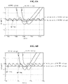
- FIGs. 6A and 6B are graphs showing an inflection point of a voltage of a source electrode of a driving thin film transistor of an organic light emitting diode display device according to a comparison example and an embodiment of the present disclosure, respectively.
- the reference voltage is supplied to the source electrode of the second TFT T2 through the reference line, and the voltage of the source electrode of the second TFT T2 varies from a voltage of the previous frame to the reference voltage.
- the variation curve of the voltage of the source electrode of the second TFT T2 has an inflection point due to influence of elements such as the third TFT T3 connected to the reference line in the next horizontal pixel line.
- the inflection point of the voltage of the source electrode of the second TFT T2 may be changed according to a state of the elements connected to the reference line.
- the source electrode of the second TFT T2 of each sub-pixel SP in the first to fifth horizontal pixel lines and the seventh to twelfth horizontal pixel lines where the turn-on section thereof overlaps the turn-on section of the next horizontal pixel line and the source electrode of the second TFT T2 of each sub-pixel SP in the sixth horizontal pixel line where the turn-on section thereof does not overlap and is separated from the turn-on section of the next horizontal pixel line have different inflection points.
- the turn-on current of the second TFT T2 becomes non-uniform and deterioration such as a horizontal bright line occurs.
- a display quality of an image is deteriorated.
- the first reference voltage REF1 is supplied to each sub-pixel SP in the odd horizontal pixel lines PR through the first reference line RL1 and the second reference voltage REF2 is supplied to each sub-pixel SP in the even horizontal pixel lines PR through the second reference line RL2 regardless of overlap of the turn-on section.
- the first reference voltage REF1 is supplied to each sub-pixel SP in the fifth horizontal pixel line PR5 where the turn-on section thereof overlaps the turn-on section of the next sixth horizontal pixel line PR6 through the first reference line RL1
- the second reference voltage REF2 is supplied to each sub-pixel SP in the sixth horizontal line PR6 where he turn-on section thereof does not overlap and is separated from the turn-on section of the next seventh horizontal pixel line through the second reference line RL2.
- the turn-on current of the second TFT T2 becomes uniform and deterioration such as a horizontal bright line is prevented.
- a total luminance increases and a display quality of an image is improved.
- the OLED display device since the reference voltage is supplied to the adjacent horizontal lines through different reference lines, deterioration such as a horizontal bright line is prevented and total luminance increases. As a result, display quality of an image is improved.
Landscapes
- Engineering & Computer Science (AREA)
- Microelectronics & Electronic Packaging (AREA)
- Physics & Mathematics (AREA)
- Geometry (AREA)
- Computer Hardware Design (AREA)
- General Physics & Mathematics (AREA)
- Theoretical Computer Science (AREA)
- Electroluminescent Light Sources (AREA)
- Control Of El Displays (AREA)
- Control Of Indicators Other Than Cathode Ray Tubes (AREA)
Description
- This patent application claims priority to Republic of
Korea Patent Application No. 10-2018-0139614, filed on November 14, 2018 - The present disclosure relates to a display device, and more particularly, to an organic light emitting diode display device where deterioration such as a horizontal bright line is prevented by supplying a reference voltage to adjacent horizontal pixel lines through different reference lines and a method of driving the organic light emitting diode display device.
- Among the flat panel displays, an organic light emitting diode (OLED) display device has a relatively high luminance and a relatively low driving voltage.
- Since the OLED display device has an emissive type, the OLED display device has a relatively great contrast ratio. In addition, since the OLED display device has a response time of several microseconds, the OLED display device has an advantage in displaying a moving image. The OLED display device also has a relatively wide viewing angle and is stable even under a relatively low temperature. Since the OLED display device is driven by a relatively low voltage of direct current (DC) 5V to 15V, a driving circuit can be easily designed and manufactured.
- Further, since the OLED display device is fabricated through a deposition and an encapsulation, the OLED display device has a simplified fabrication process.
- A plurality of thin film transistors (TFTs) such as a switching TFT, a driving TFT and a sensing TFT, a storage capacitor and a light emitting diode may be formed in each pixel of the OLED display device.
- The sensing TFT is connected to the driving TFT and a reference line to initialize a source electrode of the driving TFT by applying a reference voltage to the source electrode. A threshold voltage of the driving TFT stored in the storage capacitor is reflected to a data signal such that a variation in the threshold voltage of the driving TFT is compensated.
- The reference voltage is supplied to all the horizontal pixel lines of the OLED display device through a single reference line.
- Recently, as a resolution increases, a technology that a sufficient charging time for each pixel is obtained by partially overlapping turn-on sections of the switching TFT and the sensing TFT in the adjacent horizontal pixel lines has been developed.
- In the turn-on overlap driving, while the sensing TFT of an (n)th horizontal pixel line is turned on to initialize the source electrode of the driving TFT, the sensing TFT of an (n+1)th horizontal pixel line is also turned on. As a result, a current is instantaneously generated in the single reference line supplying the reference voltage to the (n)th and (n+1)th horizontal pixel lines, and a voltage of pthe source electrode of the driving TFT of the (n)th horizontal pixel line instantaneously increases to have an inflection point where a rate of change varies.
- The inflection point of the voltage of the source electrode of the driving TFT may influence a turn-on current of the driving TFT. When the turn-on sections of the switching TFT and the sensing TFT in all the horizontal pixel lines of the OLED display device partially overlap each other, a uniform turn-on current is generated in the driving TFT in all the horizontal pixel lines and an image displayed by the OLED display device has no deterioration.
- A technology that a response speed of an image is improved by inserting a black data into an image data has been developed.
- When the black insertion driving is applied to the turn-on overlap driving, the turn-on sections of the switching TFT and the sensing TFT do not overlap each other and are separated from each other for inserting the black data.
- The voltage of the source electrode of the driving TFT in the horizontal pixel lines where the turn-on sectons overlap each other and the voltage of the source electrode of the driving TFT in the horizontal pixel lines where the turn-on sections do not overlap each other have different inflection points according to overlap.
- When the turn-on sections of the sensing TFTs in the (n)th and (n+1)th horizontal pixel lines overlap each other and the turn-on sections of the sensing TFTs in the (n+1)th and (n+2)th horizontal pixel lines do not overlap each other and are separated from each other, the inflection point of the voltage of the source electrode of the driving TFT in the (n)th horizontal pixel line influenced by the (n+1)th horizontal pixel line becomes different from the inflection point of the voltage of the source electrode of the driving TFT in the (n+1)th horizontal pixel line influenced by the (n+2)th horizontal pixel line.
- The turn-on current becomes non-uniform due to the difference of the inflection points of the voltages of the source electrodes of the driving TFTs and deterioration such as a horizontal bright line occurs in an image displayed by the OLED display device. As a result, a display quality of the OLED display device is deteriorated.
-
US 2015/129853 A1 discloses an organic light emitting diode display device including a substrate including a display and non-display regions at a periphery of the display region with red, green, blue and white pixel regions as one pixel group formed in the display region and the display region divided into a first region and a second region; an organic light emitting diode in each of the red, green, blue and white pixel region; first to third power lines respectively disposed at an end of the first region, at an opposite end of the second region and a boundary of the first and second regions and connected to the organic light emitting diode; a first drive integrated circuit connected to the first and third power lines; and a second drive integrated circuit connected to the second and third power lines, wherein the first and second regions are symmetric with respect to the third power line. -
US 2017/157579 A1 discloses an organic light emitting display panel including an active area corresponding to an image display region, and a non-active area corresponding to a region outside of the active area, wherein the active area includes a plurality of signal lines arranged in an array, wherein the non-active area includes a pad region to which a source driver IC is mounted, and a switching structure, wherein the pad region includes a plurality of pads arranged in correspondence with the array of the signal lines, and wherein the switching structure includes: a common reference voltage pad-connection terminal connected to a common reference voltage pad of the display panel; a plurality of reference voltage line-connection terminals connected to a plurality of reference voltage lines of the display panel; and a switching circuit to switch connections between a common reference voltage pad-connection terminal and the plurality of reference voltage line-connection terminals. -
US 2015/062192 A1 discloses an organic light emitting display device including a plurality of pixels configured to each include an organic light emitting device and a pixel circuit that includes a driving transistor which supplies the data current, which is based on a difference voltage between a data voltage and a reference voltage, to the organic light emitting device, a plurality of data lines configured to respectively supply a plurality of the data voltages to the plurality of pixels, a plurality of gate lines configured to supply a gate signal to the pixels, and a plurality of reference lines connected to at least one of the pixels, and configured to supply the reference voltage to the connected pixel. The reference voltage is varied according to data of a pixel connected to a corresponding reference line. -
US 2017/221419 A1 discloses an organic light-emitting display panel including a first pixel driving circuit and a second pixel driving circuit disposed adjacent to the first pixel driving circuit along a row direction of a pixel matrix. The first pixel driving circuit is connected to a first scanning signal line, and the second pixel driving circuit is connected to a second scanning signal line. The first and the second pixel driving circuits share a same data line which is configured to time-sharingly provide an initialization signal to the first and the second pixel driving circuits, time-sharingly detect threshold voltages of driving transistors in the first and the second pixel driving circuits, and time-sharingly provide a compensated data signal to the first and the second pixel driving circuits. - The present invention concerns an organic light emitting diode display device where deterioration such as a horizontal bright line is prevented by supplying a reference voltage to adjacent horizontal pixel lines through different reference lines and a display quality is improved due to increase of a total luminance, and a method of driving the organic light emitting diode display device.
- The object is solved by the features of the independent claims. Preferred embodiments are given in the dependent claims.
- According to the present invention, an organic light emitting diode display device in accordance with claim 1 is provided.
- Classified means arranged or located.
- Preferably, the first and second reference lines may extend along a vertical direction.
- Preferably, the first and second reference lines may be alternately disposed along a horizontal direction.
- Preferably, each of a number of adjacent sub-pixels of the plurality of sub-pixels may be connected to one of the first and second reference lines through an extension line along the horizontal direction.
- Preferably, the first and second reference lines may be alternately disposed by adjacent two of the plurality of sub-pixels along a horizontal direction.
- Preferably, each of the first and second reference lines may be repeatedly disposed by adjacent four of the plurality of sub-pixels along the horizontal direction.
- Preferably, each of adjacent four of the plurality of sub-pixels may be connected to one of the first and second reference lines through an extension line along the horizontal direction.
- The plurality of sub-pixels may include first, second, third and fourth sub-pixels.
- Preferably, the first reference line may be disposed between the second and third sub-pixels and may be repeatedly disposed by the third, fourth, first and second sub-pixels.
- Preferably, the first, second, third and fourth sub-pixels may be connected to the first reference line through the extension line.
- Preferably, the second reference line may be disposed between the fourth and first sub-pixels and is repeatedly disposed by the first, second, third and fourth sub-pixels.
- Preferably, the third, fourth, first and second sub-pixels may be connected to the second reference line through the extension line.
- Each of the plurality of sub-pixels may include first, second and third thin film transistors each including a gate electrode, a source electrode and a drain electrode, a storage capacitor and a light emitting diode.
- Preferably, the gate electrode, the source electrode and the drain electrode of the first thin film transistor may be connected to the gate line, the data line and the gate electrode of the second thin film transistor, respectively.
- Preferably, the gate electrode, the source electrode and the drain electrode of the second thin film transistor may be connected to the drain electrode of the third thin film transistor, an anode of the light emitting diode and the power line, respectively.
- Preferably, the gate electrode, the source electrode and the drain electrode of the third thin film transistor may be connected to the sensing line, the source electrode of the second thin film transistor and one of the first and second reference lines, respectively.
- Preferably, the storage capacitor may be connected between the gate electrode and the source electrode of the second thin film transistor.
- Preferably, the anode and a cathode of the light emitting diode may be connected to the source electrode of the second thin film transistor and a low level voltage, respectively.
- According to one aspect of the present invention, a method of driving an organic light emitting diode in accordance with claim 9 is provided.
- Preferably, each of a number of adjacent sub-pixels of the plurality of sub-pixels may be supplied by one of the first and second reference lines through an extension line along the horizontal direction.
- Preferably, the first and second reference lines are alternately disposed by adjacent two of the plurality of sub-pixels along a horizontal direction.
- Advantages and features of the disclosure will be set forth, in part, in the description, which follows and, in part, will become apparent to those having ordinary skill in the art upon examination of the following or may be learned from practice of the disclosure. Other advantages and features of the embodiments herein may be realized and attained by the structure particularly pointed out in the written description and claims hereof as well as the appended drawings. It is to be understood that both the foregoing general description and the following detailed description are explanatory and are intended to provide further explanation of the embodiments as claimed.
- The accompanying drawings, which are included to provide a further understanding of the disclosure, are incorporated in and constitute a part of this specification, illustrate implementations of the disclosure and together with the description serve to explain the principles of embodiments of the disclosure.
-
FIG. 1 is a view showing an organic light emitting diode display device according to an embodiment of the present disclosure. -
FIG. 2 is a view showing an equivalent circuit of a sub-pixel of an organic light emitting diode according to an embodiment of the present disclosure. -
FIG. 3 is a plan view showing an organic light emitting diode display device according to an embodiment of the present disclosure. -
FIG. 4 is a cross-sectional view taken along a line IV-IV ofFIG. 3 . -
FIG. 5 is a timing chart showing a gate voltage and a sensing voltage of an organic light emitting diode display device according to an embodiment of the present disclosure. -
FIGs. 6A and 6B are graphs showing an inflection point of a voltage of a source electrode of a driving thin film transistor of an organic light emitting diode display device according to a comparison example and an embodiment of the present disclosure, respectively. - Reference will now be made in detail to embodiments of the present disclosure, examples of which are illustrated in the accompanying drawings. In the following description, when a detailed description of well-known functions or configurations related to this document is determined to unnecessarily cloud a general understanding of an embodiment of the disclosure, the detailed description thereof will be omitted. The progression of processing steps and/or operations described is an example; however, the sequence of steps and/or operations is not limited to that set forth herein and may be changed, with the exception of steps and/or operations necessarily occurring in a certain order. Like reference numerals designate like elements throughout. Names of the respective elements used in the following explanations are selected only for convenience of writing the specification and may be thus different from those used in actual products. Moreover, it is understood that terms like "horizontal" and "vertical" are used in the present application not to designate an absolute orientation in space, but only to describe relative orientations, i.e. a "horizontal" direction is understood as a direction perpendicular to a "vertical" direction, and vice versa.
-
FIG. 1 is a view showing an organic light emitting diode display device according to an embodiment of the present disclosure. - In
FIG. 1 , an organic light emitting diode (OLED)display device 110 according to an embodiment of the present disclosure includes a plurality of pixels P, and each of the plurality of pixels P includes a plurality of sub-pixels SP. - For example, each of the plurality of pixels P includes the plurality of sub-pixels SP displaying red, white, blue and green colors (R, W, B, G).
- The plurality of pixels P may be classified into a plurality of horizontal pixel lines (pixel rows). For example, the plurality of pixels P may be classified into first, second, third and fourth horizontal pixel lines PR1, PR2, PR3 and PR4. Accordingly, the plurality of sub-pixels SP included in the plurality of pixels P may be classified into first, second, third and fourth horizontal pixel lines PR1, PR2, PR3 and PR4, respectively. Within the horizontal pixel lines PR1, PR2, PR3 and PR4, the subpixels SP of each pixel P are arranged adjacent to each other along each one of the horizontal pixel lines PR1, PR2, PR3 and PR4, so that first, second third and fourth sub-pixels SP (corresponding, for example, to red, white, blue and green colors) of each pixel P follow up to each other along a respective one of the horizontal pixel lines PR1, PR2, PR3 and PR4.
- Although the
OLED display device 110 exemplarily has a stripe structure where the red, white, blue and green sub-pixels SP are disposed in the same vertical pixel line (pixel column) by color inFIG. 1 , the OLED display device may have a mosaic structure where the red, white, blue and green sub-pixels SP are disposed in the different vertical pixel line (pixel column) by color or a delta structure where the red, white, blue and green sub-pixels SP are not disposed in a line but disposed to overlap each other along a vertical direction in another embodiment. - Each of the plurality of sub-pixels SP is connected to one of first and second reference lines RL1 and RL2. The plurality of sub-pixels SP in one of the two adjacent horizontal pixel lines are connected to one of the first and second reference lines RL1 and RL2, and the plurality of sub-pixels SP in the other of the two adjacent horizontal pixel lines are connected to the other of the first and second reference lines RL1 and RL2.
- For example, the plurality of sub-pixels SP in an odd ((2k+1)th, k is 0 or a positive integer) horizontal pixel line such as the first and third horizontal pixel lines PR1 and PR3 may be connected to the first reference line RL1, and the plurality of sub-pixels SP in an even ((2k)th, k is a positive integer) horizontal pixel line such as the second and fourth horizontal pixel lines PR2 and PR4 may be connected to the second reference line RL2.
- The first and second reference lines RL1 and RL2 are disposed along a vertical direction. The first and second reference lines RL1 and RL2 are alternately disposed by the two adjacent sub-pixels SP along a horizontal direction and each of the first and second reference lines RL1 and RL2 is repeatedly disposed by the four adjacent sub-pixels SP along the horizontal direction. Each of the four adjacent sub-pixels SP along the horizontal direction is connected to one of the first and second reference lines RL1 and RL2 through an extension line along the horizontal line.
- For example, the first reference line RL1 may be disposed between the white and blue (W, B) along the vertical direction and may be repeatedly disposed by the blue, green, red and white (B, G, R, W) sub-pixels SP along the horizontal direction. The adjacent red, white, blue and green (R, W, B, G) sub-pixels SP may be connected to the first reference line RL1 through the extension line along the horizontal direction.
- In addition, the second reference line RL2 may be disposed between the green and red (G, R) along the vertical direction and may be repeatedly disposed by the red, white, blue and green (R, W, B, G) sub-pixels SP along the horizontal direction. The adjacent blue, green, red and white (B, G, R, W) sub-pixels SP may be connected to the second reference line RL2 through the extension line along the horizontal direction.
- In another embodiment, the first and second reference lines RL1 and RL2 may be disposed along a vertical direction. The first and second reference lines RL1 and RL2 may be alternately disposed by the four adjacent sub-pixels SP along a horizontal direction and may be repeatedly disposed by the eight adjacent sub-pixels SP along the horizontal direction. Each of the four adjacent sub-pixels SP along the horizontal direction may be connected to one of the first and second reference lines RL1 and RL2 through an extension line along the horizontal line.
- First and second reference voltages REF1 and REF2 may be applied to the first and second reference lines RL1 and RL2, respectively. The first and second reference voltages REF1 and REF2 may have the same value and may be a constant voltage. The first and second reference voltages REF1 and REF2 may be applied by corresponding first and second reference voltage supplies, which can be provided to supply the respective reference voltages REF1 and REF2.
- As a result, the plurality of sub-pixels SP in one of the two adjacent horizontal pixel lines are connected to one of the first and second reference lines RL1 and RL2, and one of the first and second reference voltages REF1 and REF2 is supplied to the plurality of sub-pixels SP in one of the two adjacent horizontal pixel lines. The plurality of sub-pixels SP in the other of the two adjacent horizontal pixel lines are connected to the other of the first and second reference lines RL1 and RL2, and the other of the first and second reference voltages REF1 and REF2 is supplied to the plurality of sub-pixels SP in the other of the two adjacent horizontal pixel lines.
- For example, the plurality of sub-pixels SP in an odd ((2k-1)th, k is a positive integer) horizontal pixel line such as the first and third horizontal pixel lines PR1 and PR3 may be connected to the first reference line RL1 and may receive the first reference voltage REF1. The plurality of sub-pixels SP in an even ((2k)th, k is a positive integer) horizontal pixel line such as the second and fourth horizontal pixel lines PR2 and PR4 may be connected to the second reference line RL2 and may receive the second reference voltage REF2.
- A structure of the plurality of sub-pixels SP of the
OLED display device 110 will be illustrated with reference to a drawing. -
FIG. 2 is a view showing an equivalent circuit of a sub-pixel of an organic light emitting diode according to an embodiment of the present disclosure. - In
FIG. 2 , an organic light emitting diode (OLED) display device 110 (ofFIG. 1 ) includes a plurality of sub-pixels SP (ofFIG. 1 ) such as first and second sub-pixels SP1 and SP2 adjacent to each other along a vertical direction. The first and second sub-pixels SP1 and SP2 may belong to two adjacent horizontal pixel lines, respectively. - Each of the first and second sub-pixels SP1 and SP2 may be defined by a gate line GL, a sensing line SL, a data line DL, a power line PL and first and second reference lines RL1 and RL2 crossing each other.
- A gate voltage (gate signal) GATE is supplied to the gate line GL, and a sensing voltage (sensing signal) SENS is supplied to the sensing line SL. A data voltage (data signal) DATA is supplied to the data line DL, and a high level voltage VDD is supplied to the power line PL. In addition, first and second reference voltages REF1 and REF2 are supplied to the first and second reference lines RL1 and RL2, respectively.
- For example, the gate voltage GATE and the sensing voltage SENS may be a voltage including a pulse of the same timing, and the first and second reference voltages REF1 and REF2 may be a constant voltage of the same value.
- First, second and third thin film transistors (TFTs) T1, T2 and T3, a storage capacitor Cst and a light emitting diode Del are disposed in each of the first and second sub-pixels SP1 and SP2.
- Although not shown, each of the first, second and third TFTs T1, T2 and T3 may include a gate electrode, a semiconductor layer, a source electrode and a drain electrode. A gate insulating layer may be disposed between the gate electrode and the semiconductor layer, and a passivation layer may be disposed on the source electrode and the drain electrode.
- In addition, the light emitting diode Del may include a first electrode of an anode, a light emitting layer and a second electrode of a cathode, and a color filter layer may be disposed in the plurality of sub-pixels SP.
- The gate electrode, the source electrode and the drain electrode of the first TFT T1 of a switching TFT are connected to the gate line GL, the data line DL and the gate electrode of the second TFT T2, respectively.
- The gate electrode, the source electrode and the drain electrode of the second TFT T2 of a driving TFT are connected to the drain electrode of the third TFT T3, an anode of the light emitting diode Del and the power line PL, respectively.
- The gate electrode, the source electrode and the drain electrode of the third TFT T3 of a sensing TFT are connected to the sensing line SL, the source electrode of the second TFT T2 and one of the first and second reference lines RL1 and RL2, respectively. For example, the drain electrode of the third TFT T3 in the first sub-pixel SP1 may be connected to the first reference line RL1, and the drain electrode of the third TFT T3 in the second sub-pixel SP2 may be connected to the second reference line RL2.
- The storage capacitor Cst is connected between the gate electrode and the source electrode of the second TFT T2.
- The anode and the cathode of the light emitting diode Del are connected to the source electrode of the second TFT T2 and a low level voltage VSS, respectively.
- In the
OLED display device 110, when the first TFT T1 is turned on according to the gate voltage GATE of the gate line GL, the data voltage DATA of the data line DL is applied to the gate electrode of the second TFT T2 through the first TFT T1, and the second TFT T2 supplies a current corresponding to the data voltage DATA to the light emitting diode Del using the high level voltage VDD of the power line PL. - When the third TFT T3 is turned on according to the sensing voltage SENS of the sensing line SL, the first voltage REF1 of the first reference line RL1 or the second voltage REF2 of the second reference line RL2 is applied to the source electrode of the second TFT T2, and a threshold voltage of the second TFT T2 is stored in the storage capacitor Cst.
- The threshold voltage of the second TFT T2 stored in the storage capacitor Cst in the first and second sub-pixels SP1 and SP2 is transmitted to a data driving unit (not shown) and a timing controlling unit (not shown) through the third TFT T3. The timing controlling unit generates a revised data voltage DATA by adding the threshold voltage of the second TFT T2 to the data voltage DATA and supplies the revised data voltage DATA to the first and second sub-pixels SP1 and SP2.
- A plane structure and a cross-sectional structure of the
OLED display device 110 will be illustrated with reference to a drawing. -
FIG. 3 is a plan view showing an organic light emitting diode display device according to an embodiment of the present disclosure, andFIG. 4 is a cross-sectional view taken along a line IV-IV ofFIG. 3 . - In
FIGs. 3 and 4 , a gate line GL, a sensing line SL, a data line DL, a power line PL and first and second reference lines RL1 and RL2 arc disposed on asubstrate 120 of an organic light emitting diode (OLED)display device 110 according to an embodiment of the present disclosure. - A plurality of sub-pixels SP includes red, white, blue and green sub-pixels SP(R), SP(W), SP(B) and SP(G) constituting a single pixel P, and a transistor unit TU is disposed in a lower portion of each of the plurality of sub-pixels SP.
- Each of the plurality of sub-pixels SP may include a light emitting diode Del and a color filter layer (or an overcoat layer), and the transistor unit TU may include first, second and third TFTs T1, T2 and T3 and a storage capacitor Cst.
- The plurality of pixels P may be classified into a plurality of horizontal pixel lines (pixel rows). For example, the plurality of pixels P may be classified into first, second, third and fourth horizontal pixel lines PR1, PR2, PR3 and PR4.
- A gate line GL and a sensing line SL are parallel to a horizontal direction and spaced apart from each other. A data line DL, a power line PL and first and second reference lines RL1 and RL2 are parallel to a vertical direction and spaced apart from each other.
- Although not shown, the gate line GL and the sensing line SL may include the same layer and the same material as a gate electrode of each of the first, second and third TFTs T1, T2 and T3. The data line DL, the power line PL and the first and second reference lines RL1 and RL2 may include the same layer and the same material as a source electrode and a drain electrode of each of the first, second and third TFTs T1, T2 and T3.
- Extension lines of the gate line GL, the sensing line SL and the first and second reference lines RL1 and RL2 may be spaced apart from each other between the two adjacent horizontal pixel lines and may be connected to the transistor unit TU.
- The two adjacent data lines DL may be disposed between the two adjacent sub-pixels SP and may be repeatedly disposed by the two adjacent sub-pixels SP along the horizontal direction. The two adjacent data lines DL may be connected to the transistor unit TU.
- The power line PL may be disposed along the vertical direction. The power line PL may be alternately disposed with the first reference line RL1 or the second reference line RL2 by the two adjacent sub-pixels SP along the horizontal direction. The power line PL may be repeatedly disposed by the four adjacent sub-pixels SP along the horizontal direction. The transistor unit TU of the four adjacent sub-pixels SP along the horizontal direction may be connected to the power line through the extension line along the horizontal direction.
- The first and second reference lines RL1 and RL2 may be disposed along the vertical direction. The first and second reference lines RL1 and RL2 may be alternately disposed by the two adjacent sub-pixels SP along the horizontal direction and may be repeatedly disposed by the four adjacent sub-pixels SP along the horizontal direction. The transistor unit TU of the four adjacent sub-pixels SP along the horizontal direction may be connected to one of the first and second reference lines RL1 and RL2 through the extension line along the horizontal direction.
- For example, the first reference line RL1 may be disposed between the white and blue (W, B) sub-pixels SP along the vertical direction and may be repeatedly disposed by the blue, green, red and white (B, G, R, W) sub-pixels SP along the horizontal direction. The transistor unit TU of the adjacent red, white, blue and green (R, W, B, G) sub-pixels SP may be connected to the first reference line RL1 through the extension line along the horizontal direction.
- The second reference line RL2 may be disposed between the green and red (G, R) sub-pixels SP along the vertical direction and may be repeatedly disposed by the red, white, blue and green (R, W, B, G) sub-pixels SP along the horizontal direction. The transistor unit TU of the adjacent blue, green, red and white (B, G, R, W) sub-pixels SP may be connected to the second reference line RL2 through the extension line along the horizontal direction.
- A gate voltage (gate signal) GATE is supplied to the gate line GL, and a sensing voltage (sensing signal) SENS is supplied to the sensing line SL. A data voltage (data signal) DATA is supplied to the data line DL, and a high level voltage VDD is supplied to the power line PL. In addition, first and second reference voltages REF1 and REF2 are supplied to the first and second reference lines RL1 and RL2, respectively.
- The gate voltage GATE and the sensing voltage SENS may have the same timing.
-
FIG. 5 is a timing chart showing a gate voltage and a sensing voltage of an organic light emitting diode display device according to an embodiment of the present disclosure. - In
FIG. 5 , a gate voltage GATE and a sensing voltage SENS are supplied to a gate line GL (ofFIG. 3 ) and a sensing line SL (ofFIG. 3 ), respectively, of each horizontal pixel line PR (ofFIG. 3 ) of an organic light emitting diode (OLED) display device 110 (ofFIG. 3 ). The gate voltage GATE and the sensing voltage SENS may be a voltage including a pulse of the same timing. - The plurality of sub-pixels SP in an odd ((2k+1)th, k is 0 or a positive integer) horizontal pixel line PR may be connected to the first reference line RL1 to receive a first reference voltage REF1. The plurality of sub-pixels SP in an even ((2k)th, k is a positive integer) horizontal pixel line PR may be connected to the second reference line RL2 to receive a second reference voltage REF2.
- For example, a first gate voltage GATE1 and a first sensing voltage SENS1 may be supplied to the gate line GL and the sensing line SL, respectively, in a first horizontal pixel line PR1, and a second gate voltage GATE2 and a second sensing voltage SENS2 may be supplied to the gate line GL and the sensing line SL, respectively, in a second horizontal pixel line PR2.
- Similarly, third to twelfth gate voltages GATE3 to GATE12 may be supplied to the gate line GL in third to twelfth horizontal pixel lines, respectively, and third to twelfth sensing voltages SENS3 to SENS12 may be supplied to the sensing line SL in third to twelfth horizontal pixel lines, respectively.
- Each of the first to twelfth sensing voltages SENS1 to SENS12 includes a pulse having a turn-on section of a high level, and the turn-on section of the pulse corresponds to two
horizontal period 2H of theOLED display device 110. - A timing of the turn-on section of the first to twelfth sensing voltages SENS1 to SENS12 may be sequentially changed according to the horizontal pixel line PR.
- To obtain a sufficient charging time, the turn-on sections of adjacent two of the first to sixth sensing voltages SENS1 to SENS6 partially overlap each other by one
horizontal period 1H and the turn-on sections of adjacent two of the seventh to twelfth sensing voltages SENS7 to SENS12 partially overlap each other by onehorizontal period 1H. - In addition, to insert a black data for prevention of a residual image, the turn-on sections of the sixth and seventh sensing voltages SENS6 and SENS7 do not overlap each other and are separated from each other.
- In the
OLED display device 110 driven by the sensing voltage SENS, deterioration such as a horizontal bright line may be prevented by supplying the first and second reference voltages REF1 and REF2 to the two adjacent horizontal pixel lines through the first and second reference lines RL1 and RL2, respectively. -
FIGs. 6A and 6B are graphs showing an inflection point of a voltage of a source electrode of a driving thin film transistor of an organic light emitting diode display device according to a comparison example and an embodiment of the present disclosure, respectively. - In
FIGs. 6A and 6B , when the third thin film transistor (TFT) T3 is turned on by the sensing voltage SENS in each of the sub-pixels of the first to twelfth horizontal pixel lines of the organic light emitting diode (OLED) display device according to a comparison example and an embodiment of the present disclosure, the reference voltage is supplied to the source electrode of the second TFT T2 through the reference line, and the voltage of the source electrode of the second TFT T2 varies from a voltage of the previous frame to the reference voltage. The variation curve of the voltage of the source electrode of the second TFT T2 has an inflection point due to influence of elements such as the third TFT T3 connected to the reference line in the next horizontal pixel line. - The inflection point of the voltage of the source electrode of the second TFT T2 may be changed according to a state of the elements connected to the reference line.
- As shown in
FIG. 6A of the OLED display device according to the comparison example where the reference voltage is supplied to each sub-pixel in the first to twelfth horizontal pixel lines through one reference line, the source electrode of the second TFT T2 of each sub-pixel SP in the first to fifth horizontal pixel lines and the seventh to twelfth horizontal pixel lines where the turn-on section thereof overlaps the turn-on section of the next horizontal pixel line and the source electrode of the second TFT T2 of each sub-pixel SP in the sixth horizontal pixel line where the turn-on section thereof does not overlap and is separated from the turn-on section of the next horizontal pixel line have different inflection points. - The voltage of the source electrode (N1(PR5)) of the second TFT T2 of each sub-pixel SP in the fifth horizontal pixel line PR5 where the turn-on section thereof overlaps the turn-on section of the next sixth horizontal pixel line PR6 and the voltage of the source electrode (N1(PR6)) of the second TFT T2 of each sub-pixel SP in the sixth horizontal pixel line PR6 where the turn-on section thereof does not overlap and is separated from the turn-on section of the next seventh horizontal pixel line have different inflection points. As a result, the turn-on current of the second TFT T2 becomes non-uniform and deterioration such as a horizontal bright line occurs. As a result, a display quality of an image is deteriorated.
- As shown in
FIG. 6B of theOLED display device 110 according to an embodiment of the present disclosure, the first reference voltage REF1 is supplied to each sub-pixel SP in the odd horizontal pixel lines PR through the first reference line RL1 and the second reference voltage REF2 is supplied to each sub-pixel SP in the even horizontal pixel lines PR through the second reference line RL2 regardless of overlap of the turn-on section. - For example, the first reference voltage REF1 is supplied to each sub-pixel SP in the fifth horizontal pixel line PR5 where the turn-on section thereof overlaps the turn-on section of the next sixth horizontal pixel line PR6 through the first reference line RL1, and the second reference voltage REF2 is supplied to each sub-pixel SP in the sixth horizontal line PR6 where he turn-on section thereof does not overlap and is separated from the turn-on section of the next seventh horizontal pixel line through the second reference line RL2.
- The voltage of the source electrode (N1(PR5)) of the second TFT T2 of each sub-pixel SP in the fifth horizontal pixel line PR5 where the turn-on section thereof overlaps the turn-on section of the next sixth horizontal pixel line PR6 and the voltage of the source electrode (N1(PR6)) of the second TFT T2 of each sub-pixel SP in the sixth horizontal pixel line PR6 where the turn-on section thereof does not overlap and is separated from the turn-on section of the next seventh horizontal pixel line have the same inflection points as each other. As a result, the turn-on current of the second TFT T2 becomes uniform and deterioration such as a horizontal bright line is prevented. As a result, a total luminance increases and a display quality of an image is improved.
- Consequently, in the OLED display device according to the present disclosure, since the reference voltage is supplied to the adjacent horizontal lines through different reference lines, deterioration such as a horizontal bright line is prevented and total luminance increases. As a result, display quality of an image is improved.
Claims (11)
- An organic light emitting diode display device (110), comprising:a substrate (120) including a plurality of sub-pixels (SP) classified into a plurality of horizontal pixel lines (PR1, PR2, PR3, PR4);a gate line (GL) and a sensing line (SL) spaced apart from each other on the substrate (120);a data line (DL) and a power line (PL) crossing the gate line (GL) and the sensing line (SL) and spaced apart from each other; andfirst and second reference lines (RL1, RL2) supplying first and second reference voltages (REF1, REF2), respectively, and connected to adjacent two, respectively, of the plurality of horizontal pixel lines,characterized in that the display device is configured to supply the first reference voltage (REF1) to the plurality of sub-pixels (SP) in odd ones of the plurality of horizontal pixel lines (PR1, PR2, PR3, PR4) through the first reference line (RL1), andconfigured to supply the second reference voltage (REF2) to the plurality of sub-pixels (SP) in even ones of the plurality of horizontal pixel lines (PR1, PR2, PR3, PR4) through the second reference line (RL2),wherein the plurality of horizontal pixel lines (PR1, PR2, PR3, PR4) include (n)th, (n+1)th and (n+2)th horizontal pixel lines, means for providing that turn-on sections of sensing voltages (SENS) supplied to the (n)th and (n+1)th horizontal pixel lines overlap each other, and the turn-on sections of the sensing voltages (SENS) supplied to the (n+1)th and (n+2)th horizontal pixel lines are separated from each other, andwherein the first reference voltage (REF1) is supplied to the plurality of sub-pixels (SP) in the (n)th horizontal pixel line through the first reference line (RL1), and the second reference voltage (REF2) is supplied to the plurality of sub-pixels (SP) in the (n+1)th horizontal pixel line through the second reference line (RL2).
- The display device of claim 1, wherein the first and second reference lines (RL1, RL2) extend along a vertical direction.
- The display device of claim 2, wherein the first and second reference lines (RL1, RL2) are alternately disposed along a horizontal direction.
- The display device of claim 3, wherein each of a number of adjacent sub-pixels (SP) of the plurality of sub-pixels (SP) is connected to one of the first and second reference lines (RL1, RL2) through an extension line along the horizontal direction.
- The display device of claim 3 or 4, wherein the first and second reference lines (RL1, RL2) are alternately disposed by adjacent two of the plurality of sub-pixels (SP) along a horizontal direction.
- The display device of claim 5, wherein each of the first and second reference lines (RL1, RL2) is repeatedly disposed by adjacent four of the plurality of sub-pixels (SP) along the horizontal direction, and
wherein each of adjacent four of the plurality of sub-pixels (SP) is connected to one of the first and second reference lines (RL1, RL2) through an extension line along the horizontal direction. - The display device of claim 6, wherein the plurality of sub-pixels (SP) include first, second, third and fourth sub-pixels,wherein the first reference line (RL1) is disposed between the second and third sub-pixels (SP) and is repeatedly disposed by the third, fourth, first and second sub-pixels (SP),wherein the first, second, third and fourth sub-pixels (SP) are connected to the first reference line (RL1) through the extension line,wherein the second reference line (RL2) is disposed between the fourth and first sub-pixels (SP) and is repeatedly disposed by the first, second, third and fourth sub-pixels (SP), andwherein the third, fourth, first and second sub-pixels (SP) are connected to the second reference line (RL2) through the extension line.
- The display device of any one of claims 1 to 7, wherein each of the plurality of sub-pixels (SP) includes first, second and third thin film transistors (T1, T2, T3) each including a gate electrode, a source electrode and a drain electrode, a storage capacitor (Cst) and a light emitting diode (Del),wherein the gate electrode, the source electrode and the drain electrode of the first thin film transistor (T1) are connected to the gate line (GL), the data line (DL) and the gate electrode of the second thin film transistor (T2), respectively,wherein the gate electrode, the source electrode and the drain electrode of the second thin film transistor (T2) are connected to the drain electrode of the third thin film transistor (T3), an an-ode of the light emitting diode (Del) and the power line (PL), respectively,wherein the gate electrode, the source electrode and the drain electrode of the third thin film transistor (T3) are connected to the sensing line (SL), the source electrode of the second thin film transistor (T2) and one of the first and second reference lines (RL1, RL2), respectively,wherein the storage capacitor (Cst) is connected between the gate electrode and the source electrode of the second thin film transistor (T2), andwherein the anode and a cathode of the light emitting diode (Del) are connected to the source electrode of the second thin film transistor (T2) and a low level voltage (VSS), respectively.
- A method of driving an organic light emitting diode including a plurality of sub-pixels (SP) classified into a plurality of horizontal pixel lines (PR1, PR2, PR3, PR4), comprising:supplying a gate voltage (GATE) to the plurality of sub-pixels (SP) in the plurality of horizontal pixel lines (PR1, PR2, PR3, PR4) through a gate line (GL);supplying a data voltage (DATA) to the plurality of sub-pixels (SP) in the plurality of horizontal pixel lines (PR1, PR2, PR3, PR4) through a data line (DL);supplying a sensing voltage (SENS) to the plurality of sub-pixels (SP) in the plurality of horizontal pixel lines (PR1, PR2, PR3, PR4) through a sensing line (SL); andsupplying first and second reference voltages (REF1, REF2) to adjacent two, respectively, of the plurality of horizontal pixel lines (PR1, PR2, PR3, PR4) through first and second reference lines (RL1, RL2), respectively,characterized in that supplying the first and second reference voltages (REF1, REF2) comprises:supplying the first reference voltage (REF1) to the plurality of sub-pixels (SP) in odd ones of the plurality of horizontal pixel lines (PR1, PR2, PR3, PR4) through the first reference line (RL1); andsupplying the second reference voltage (REF2) to the plurality of sub-pixels (SP) in even ones of the plurality of horizontal pixel lines (PR1, PR2, PR3, PR4) through the second reference line (RL2),wherein the plurality of horizontal pixel lines (PR1, PR2, PR3, PR4) include (n)th, (n+1)th and (n+2)th horizontal pixel lines,wherein turn-on sections of sensing voltages supplied to the (n)th and (n+1)th horizontal pixel lines overlap each other, and the turn-on sections of the sensing voltages (SENS) supplied to the (n+1)th and (n+2)th horizontal pixel lines are separated from each other, andwherein the first reference voltage (REF1) is supplied to the plurality of sub-pixels (SP) in the (n)th horizontal pixel line through the first reference line (RL1), and the second reference voltage (REF2) is supplied to the plurality of sub-pixels (SP) in the (n+1)th horizontal pixel line through the second reference line (RL2).
- The method of claim 9, wherein each of a number of adjacent sub-pixels (SP) of the plurality of sub-pixels (SP) is supplied by one of the first and second reference lines (RL1, RL2) through an extension line along the horizontal direction.
- The method of claim 9 or 10, wherein the first and second reference lines (RL1, RL2) are alternately disposed by adjacent two of the plurality of sub-pixels (SP) along a horizontal direction.
Applications Claiming Priority (1)
| Application Number | Priority Date | Filing Date | Title |
|---|---|---|---|
| KR1020180139614A KR102596755B1 (en) | 2018-11-14 | 2018-11-14 | Organic Light Emitting Diode Display Device And Method Of Driving The Same |
Publications (2)
| Publication Number | Publication Date |
|---|---|
| EP3654379A1 EP3654379A1 (en) | 2020-05-20 |
| EP3654379B1 true EP3654379B1 (en) | 2022-08-31 |
Family
ID=68502955
Family Applications (1)
| Application Number | Title | Priority Date | Filing Date |
|---|---|---|---|
| EP19207773.3A Active EP3654379B1 (en) | 2018-11-14 | 2019-11-07 | Organic light emitting diode display device and method of driving the same |
Country Status (4)
| Country | Link |
|---|---|
| US (1) | US11580909B2 (en) |
| EP (1) | EP3654379B1 (en) |
| KR (1) | KR102596755B1 (en) |
| CN (1) | CN111192901B (en) |
Families Citing this family (8)
| Publication number | Priority date | Publication date | Assignee | Title |
|---|---|---|---|---|
| KR102526291B1 (en) * | 2018-07-24 | 2023-04-27 | 엘지디스플레이 주식회사 | Organic Emitting Diode Display Device |
| CN116564209A (en) * | 2019-02-23 | 2023-08-08 | 华为技术有限公司 | Method and electronic device for displaying images in multi-display driving circuit system |
| CN110060633B (en) * | 2019-05-23 | 2021-10-15 | 合肥鑫晟光电科技有限公司 | A display panel, its driving method and display device |
| KR102866495B1 (en) * | 2020-07-23 | 2025-09-29 | 엘지디스플레이 주식회사 | Transparent display device |
| CN114616669B (en) * | 2020-08-31 | 2026-01-30 | 京东方科技集团股份有限公司 | A display substrate, its manufacturing method, and a display device. |
| CN112863438A (en) * | 2021-01-19 | 2021-05-28 | 武汉华星光电半导体显示技术有限公司 | Display panel and display device |
| KR102810624B1 (en) * | 2021-02-23 | 2025-05-22 | 삼성디스플레이 주식회사 | Pixel circuit, display apparatus including the same and method of driving the same |
| CN115132139B (en) * | 2022-06-27 | 2023-07-18 | 绵阳惠科光电科技有限公司 | Display driving circuit and display device |
Family Cites Families (26)
| Publication number | Priority date | Publication date | Assignee | Title |
|---|---|---|---|---|
| JP2801487B2 (en) | 1992-04-30 | 1998-09-21 | シャープ株式会社 | Panel mounting structure, mounting method, and resin supply curing method |
| JP2006039457A (en) * | 2004-07-30 | 2006-02-09 | Oki Electric Ind Co Ltd | Scanning method for display panel and display device |
| JP4551712B2 (en) * | 2004-08-06 | 2010-09-29 | 東芝モバイルディスプレイ株式会社 | Gate line drive circuit |
| JP2006058638A (en) * | 2004-08-20 | 2006-03-02 | Toshiba Matsushita Display Technology Co Ltd | Gate line driving circuit |
| US7586476B2 (en) * | 2005-06-15 | 2009-09-08 | Lg. Display Co., Ltd. | Apparatus and method for driving liquid crystal display device |
| KR101169053B1 (en) * | 2005-06-30 | 2012-07-26 | 엘지디스플레이 주식회사 | Organic Light Emitting Diode Display |
| US8736535B2 (en) * | 2007-03-29 | 2014-05-27 | Nlt Technologies, Ltd. | Hold type image display system |
| KR101298438B1 (en) * | 2008-02-27 | 2013-08-20 | 엘지디스플레이 주식회사 | Liquid Crystal Display and Driving Method thereof |
| JP2013167772A (en) * | 2012-02-16 | 2013-08-29 | Panasonic Liquid Crystal Display Co Ltd | Liquid crystal display device |
| US9280231B2 (en) * | 2012-06-20 | 2016-03-08 | Synaptics Incorporated | Disabling display lines during input sensing periods |
| KR101528148B1 (en) * | 2012-07-19 | 2015-06-12 | 엘지디스플레이 주식회사 | Organic light emitting diode display device having for sensing pixel current and method of sensing the same |
| KR102016562B1 (en) * | 2013-07-31 | 2019-08-30 | 엘지디스플레이 주식회사 | Organic Light Emitting Display |
| KR102050268B1 (en) | 2013-08-30 | 2019-12-02 | 엘지디스플레이 주식회사 | Organic light emitting display device |
| KR102100261B1 (en) * | 2013-11-13 | 2020-04-13 | 엘지디스플레이 주식회사 | Organic light emitting diode display device and repairing method thereof |
| KR102101182B1 (en) * | 2013-12-23 | 2020-04-16 | 엘지디스플레이 주식회사 | Organic light emitting display device |
| KR102083458B1 (en) * | 2013-12-26 | 2020-03-02 | 엘지디스플레이 주식회사 | Organic Light Emitting Display and Image Quality Compensation Method Of The Same |
| CN104269431B (en) * | 2014-09-29 | 2017-03-01 | 京东方科技集团股份有限公司 | A kind of organic elctroluminescent device, its driving method and display device |
| KR102333739B1 (en) * | 2014-10-06 | 2021-12-01 | 엘지디스플레이 주식회사 | Organic electro luminescent display device and transitor structure for display device |
| KR102281817B1 (en) | 2014-11-11 | 2021-07-23 | 엘지디스플레이 주식회사 | Organic light emmiting diode display device and driving method of the same |
| KR102262858B1 (en) * | 2015-05-29 | 2021-06-09 | 엘지디스플레이 주식회사 | Data driver, organic light emitting display panel, organic light emitting display device, and method for driving the organic light emitting display device |
| KR102216705B1 (en) * | 2015-06-30 | 2021-02-18 | 엘지디스플레이 주식회사 | Source driver ic, controller, organic light emitting display panel, organic light emitting display device, and the method for driving the organic light emitting display device |
| KR102427312B1 (en) * | 2015-11-27 | 2022-08-01 | 엘지디스플레이 주식회사 | Organic light-emitting display panel and organic light-emitting display device |
| KR102396465B1 (en) * | 2015-12-30 | 2022-05-10 | 엘지디스플레이 주식회사 | Organic Light Emitting Display Device |
| CN106125435A (en) * | 2016-08-31 | 2016-11-16 | 深圳市华星光电技术有限公司 | Liquid crystal panel and liquid crystal display |
| KR102526355B1 (en) * | 2016-09-22 | 2023-05-02 | 엘지디스플레이 주식회사 | Organic Light Emitting Display Device |
| CN106531084B (en) | 2017-01-05 | 2019-02-05 | 上海天马有机发光显示技术有限公司 | Organic light-emitting display panel and driving method thereof, and organic light-emitting display device |
-
2018
- 2018-11-14 KR KR1020180139614A patent/KR102596755B1/en active Active
-
2019
- 2019-11-04 CN CN201911065385.9A patent/CN111192901B/en active Active
- 2019-11-06 US US16/676,297 patent/US11580909B2/en active Active
- 2019-11-07 EP EP19207773.3A patent/EP3654379B1/en active Active
Also Published As
| Publication number | Publication date |
|---|---|
| KR102596755B1 (en) | 2023-10-31 |
| CN111192901B (en) | 2023-11-14 |
| KR20200055928A (en) | 2020-05-22 |
| EP3654379A1 (en) | 2020-05-20 |
| US11580909B2 (en) | 2023-02-14 |
| US20200152126A1 (en) | 2020-05-14 |
| CN111192901A (en) | 2020-05-22 |
Similar Documents
| Publication | Publication Date | Title |
|---|---|---|
| EP3654379A1 (en) | Organic light emitting diode display device and method of driving the same | |
| US8754913B2 (en) | Subpixel arrangement structure of display device | |
| USRE48044E1 (en) | Organic electroluminescence emitting display | |
| US9368064B2 (en) | Display panel, display apparatus, and electronic system | |
| US8411016B2 (en) | Scanning drive circuit and display device including the same | |
| US12550515B2 (en) | Display device including an optical sensor on an area overlapping an active area of a display panel | |
| US20120242708A1 (en) | Active matrix electroluminescent display | |
| JP2014029424A (en) | Display device, electronic apparatus, and display panel drive method | |
| KR102763606B1 (en) | Display Device Including Dual Data Lines | |
| US20240071307A1 (en) | Display panel and electroluminescent display device including the same and pixel driving circuit | |
| US20230316999A1 (en) | Method for image display in a display apparatus, display apparatus, peripheral sensing circuit, and pixel driving circuit | |
| US10910444B2 (en) | Display panel | |
| US20190197961A1 (en) | Display Device | |
| CN119631126A (en) | Display Devices | |
| JP2009111047A (en) | Color image display device, shadow mask, and method of manufacturing color image display device using shadow mask | |
| KR100774911B1 (en) | Electro luminescence display | |
| US10482816B2 (en) | Method for driving display element, display device, and electronic device | |
| CN116403525B (en) | Organic light-emitting diode display device including compensation unit and driving method thereof | |
| US11769435B2 (en) | Deformed display device | |
| JP2023095533A (en) | Display panel and display device | |
| US20260136734A1 (en) | Display device including an optical sensor on an area overlapping an active area of a display panel | |
| US20250275394A1 (en) | Display Apparatus | |
| US20260087994A1 (en) | Display Device | |
| CN116386538B (en) | Organic light-emitting diode display device including compensation unit and driving method thereof | |
| WO2026045054A1 (en) | Pixel driving circuit and driving method therefor, and display device |
Legal Events
| Date | Code | Title | Description |
|---|---|---|---|
| PUAI | Public reference made under article 153(3) epc to a published international application that has entered the european phase |
Free format text: ORIGINAL CODE: 0009012 |
|
| STAA | Information on the status of an ep patent application or granted ep patent |
Free format text: STATUS: REQUEST FOR EXAMINATION WAS MADE |
|
| 17P | Request for examination filed |
Effective date: 20191107 |
|
| AK | Designated contracting states |
Kind code of ref document: A1 Designated state(s): AL AT BE BG CH CY CZ DE DK EE ES FI FR GB GR HR HU IE IS IT LI LT LU LV MC MK MT NL NO PL PT RO RS SE SI SK SM TR |
|
| AX | Request for extension of the european patent |
Extension state: BA ME |
|
| RBV | Designated contracting states (corrected) |
Designated state(s): AL AT BE BG CH CY CZ DE DK EE ES FI FR GB GR HR HU IE IS IT LI LT LU LV MC MK MT NL NO PL PT RO RS SE SI SK SM TR |
|
| GRAP | Despatch of communication of intention to grant a patent |
Free format text: ORIGINAL CODE: EPIDOSNIGR1 |
|
| STAA | Information on the status of an ep patent application or granted ep patent |
Free format text: STATUS: GRANT OF PATENT IS INTENDED |
|
| INTG | Intention to grant announced |
Effective date: 20220323 |
|
| GRAS | Grant fee paid |
Free format text: ORIGINAL CODE: EPIDOSNIGR3 |
|
| GRAA | (expected) grant |
Free format text: ORIGINAL CODE: 0009210 |
|
| STAA | Information on the status of an ep patent application or granted ep patent |
Free format text: STATUS: THE PATENT HAS BEEN GRANTED |
|
| AK | Designated contracting states |
Kind code of ref document: B1 Designated state(s): AL AT BE BG CH CY CZ DE DK EE ES FI FR GB GR HR HU IE IS IT LI LT LU LV MC MK MT NL NO PL PT RO RS SE SI SK SM TR |
|
| REG | Reference to a national code |
Ref country code: CH Ref legal event code: EP Ref country code: GB Ref legal event code: FG4D |
|
| REG | Reference to a national code |
Ref country code: AT Ref legal event code: REF Ref document number: 1515933 Country of ref document: AT Kind code of ref document: T Effective date: 20220915 |
|
| REG | Reference to a national code |
Ref country code: DE Ref legal event code: R096 Ref document number: 602019018903 Country of ref document: DE |
|
| REG | Reference to a national code |
Ref country code: IE Ref legal event code: FG4D |
|
| REG | Reference to a national code |
Ref country code: DE Ref legal event code: R079 Ref document number: 602019018903 Country of ref document: DE Free format text: PREVIOUS MAIN CLASS: H01L0027320000 Ipc: H10K0059000000 |
|
| REG | Reference to a national code |
Ref country code: LT Ref legal event code: MG9D |
|
| REG | Reference to a national code |
Ref country code: NL Ref legal event code: MP Effective date: 20220831 |
|
| PG25 | Lapsed in a contracting state [announced via postgrant information from national office to epo] |
Ref country code: SE Free format text: LAPSE BECAUSE OF FAILURE TO SUBMIT A TRANSLATION OF THE DESCRIPTION OR TO PAY THE FEE WITHIN THE PRESCRIBED TIME-LIMIT Effective date: 20220831 Ref country code: RS Free format text: LAPSE BECAUSE OF FAILURE TO SUBMIT A TRANSLATION OF THE DESCRIPTION OR TO PAY THE FEE WITHIN THE PRESCRIBED TIME-LIMIT Effective date: 20220831 Ref country code: NO Free format text: LAPSE BECAUSE OF FAILURE TO SUBMIT A TRANSLATION OF THE DESCRIPTION OR TO PAY THE FEE WITHIN THE PRESCRIBED TIME-LIMIT Effective date: 20221130 Ref country code: LV Free format text: LAPSE BECAUSE OF FAILURE TO SUBMIT A TRANSLATION OF THE DESCRIPTION OR TO PAY THE FEE WITHIN THE PRESCRIBED TIME-LIMIT Effective date: 20220831 Ref country code: LT Free format text: LAPSE BECAUSE OF FAILURE TO SUBMIT A TRANSLATION OF THE DESCRIPTION OR TO PAY THE FEE WITHIN THE PRESCRIBED TIME-LIMIT Effective date: 20220831 Ref country code: FI Free format text: LAPSE BECAUSE OF FAILURE TO SUBMIT A TRANSLATION OF THE DESCRIPTION OR TO PAY THE FEE WITHIN THE PRESCRIBED TIME-LIMIT Effective date: 20220831 |
|
| REG | Reference to a national code |
Ref country code: AT Ref legal event code: MK05 Ref document number: 1515933 Country of ref document: AT Kind code of ref document: T Effective date: 20220831 |
|
| PG25 | Lapsed in a contracting state [announced via postgrant information from national office to epo] |
Ref country code: PL Free format text: LAPSE BECAUSE OF FAILURE TO SUBMIT A TRANSLATION OF THE DESCRIPTION OR TO PAY THE FEE WITHIN THE PRESCRIBED TIME-LIMIT Effective date: 20220831 Ref country code: IS Free format text: LAPSE BECAUSE OF FAILURE TO SUBMIT A TRANSLATION OF THE DESCRIPTION OR TO PAY THE FEE WITHIN THE PRESCRIBED TIME-LIMIT Effective date: 20221231 Ref country code: HR Free format text: LAPSE BECAUSE OF FAILURE TO SUBMIT A TRANSLATION OF THE DESCRIPTION OR TO PAY THE FEE WITHIN THE PRESCRIBED TIME-LIMIT Effective date: 20220831 Ref country code: GR Free format text: LAPSE BECAUSE OF FAILURE TO SUBMIT A TRANSLATION OF THE DESCRIPTION OR TO PAY THE FEE WITHIN THE PRESCRIBED TIME-LIMIT Effective date: 20221201 |
|
| PG25 | Lapsed in a contracting state [announced via postgrant information from national office to epo] |
Ref country code: SM Free format text: LAPSE BECAUSE OF FAILURE TO SUBMIT A TRANSLATION OF THE DESCRIPTION OR TO PAY THE FEE WITHIN THE PRESCRIBED TIME-LIMIT Effective date: 20220831 Ref country code: RO Free format text: LAPSE BECAUSE OF FAILURE TO SUBMIT A TRANSLATION OF THE DESCRIPTION OR TO PAY THE FEE WITHIN THE PRESCRIBED TIME-LIMIT Effective date: 20220831 Ref country code: PT Free format text: LAPSE BECAUSE OF FAILURE TO SUBMIT A TRANSLATION OF THE DESCRIPTION OR TO PAY THE FEE WITHIN THE PRESCRIBED TIME-LIMIT Effective date: 20230102 Ref country code: ES Free format text: LAPSE BECAUSE OF FAILURE TO SUBMIT A TRANSLATION OF THE DESCRIPTION OR TO PAY THE FEE WITHIN THE PRESCRIBED TIME-LIMIT Effective date: 20220831 Ref country code: DK Free format text: LAPSE BECAUSE OF FAILURE TO SUBMIT A TRANSLATION OF THE DESCRIPTION OR TO PAY THE FEE WITHIN THE PRESCRIBED TIME-LIMIT Effective date: 20220831 Ref country code: CZ Free format text: LAPSE BECAUSE OF FAILURE TO SUBMIT A TRANSLATION OF THE DESCRIPTION OR TO PAY THE FEE WITHIN THE PRESCRIBED TIME-LIMIT Effective date: 20220831 Ref country code: AT Free format text: LAPSE BECAUSE OF FAILURE TO SUBMIT A TRANSLATION OF THE DESCRIPTION OR TO PAY THE FEE WITHIN THE PRESCRIBED TIME-LIMIT Effective date: 20220831 |
|
| PG25 | Lapsed in a contracting state [announced via postgrant information from national office to epo] |
Ref country code: SK Free format text: LAPSE BECAUSE OF FAILURE TO SUBMIT A TRANSLATION OF THE DESCRIPTION OR TO PAY THE FEE WITHIN THE PRESCRIBED TIME-LIMIT Effective date: 20220831 Ref country code: EE Free format text: LAPSE BECAUSE OF FAILURE TO SUBMIT A TRANSLATION OF THE DESCRIPTION OR TO PAY THE FEE WITHIN THE PRESCRIBED TIME-LIMIT Effective date: 20220831 |
|
| REG | Reference to a national code |
Ref country code: DE Ref legal event code: R097 Ref document number: 602019018903 Country of ref document: DE |
|
| PG25 | Lapsed in a contracting state [announced via postgrant information from national office to epo] |
Ref country code: NL Free format text: LAPSE BECAUSE OF FAILURE TO SUBMIT A TRANSLATION OF THE DESCRIPTION OR TO PAY THE FEE WITHIN THE PRESCRIBED TIME-LIMIT Effective date: 20220831 Ref country code: MC Free format text: LAPSE BECAUSE OF FAILURE TO SUBMIT A TRANSLATION OF THE DESCRIPTION OR TO PAY THE FEE WITHIN THE PRESCRIBED TIME-LIMIT Effective date: 20220831 Ref country code: AL Free format text: LAPSE BECAUSE OF FAILURE TO SUBMIT A TRANSLATION OF THE DESCRIPTION OR TO PAY THE FEE WITHIN THE PRESCRIBED TIME-LIMIT Effective date: 20220831 |
|
| REG | Reference to a national code |
Ref country code: CH Ref legal event code: PL |
|
| PLBE | No opposition filed within time limit |
Free format text: ORIGINAL CODE: 0009261 |
|
| STAA | Information on the status of an ep patent application or granted ep patent |
Free format text: STATUS: NO OPPOSITION FILED WITHIN TIME LIMIT |
|
| REG | Reference to a national code |
Ref country code: BE Ref legal event code: MM Effective date: 20221130 |
|
| PG25 | Lapsed in a contracting state [announced via postgrant information from national office to epo] |
Ref country code: LI Free format text: LAPSE BECAUSE OF NON-PAYMENT OF DUE FEES Effective date: 20221130 Ref country code: CH Free format text: LAPSE BECAUSE OF NON-PAYMENT OF DUE FEES Effective date: 20221130 |
|
| 26N | No opposition filed |
Effective date: 20230601 |
|
| PG25 | Lapsed in a contracting state [announced via postgrant information from national office to epo] |
Ref country code: SI Free format text: LAPSE BECAUSE OF FAILURE TO SUBMIT A TRANSLATION OF THE DESCRIPTION OR TO PAY THE FEE WITHIN THE PRESCRIBED TIME-LIMIT Effective date: 20220831 Ref country code: LU Free format text: LAPSE BECAUSE OF NON-PAYMENT OF DUE FEES Effective date: 20221107 |
|
| PG25 | Lapsed in a contracting state [announced via postgrant information from national office to epo] |
Ref country code: IE Free format text: LAPSE BECAUSE OF NON-PAYMENT OF DUE FEES Effective date: 20221107 |
|
| PG25 | Lapsed in a contracting state [announced via postgrant information from national office to epo] |
Ref country code: BE Free format text: LAPSE BECAUSE OF NON-PAYMENT OF DUE FEES Effective date: 20221130 |
|
| PG25 | Lapsed in a contracting state [announced via postgrant information from national office to epo] |
Ref country code: HU Free format text: LAPSE BECAUSE OF FAILURE TO SUBMIT A TRANSLATION OF THE DESCRIPTION OR TO PAY THE FEE WITHIN THE PRESCRIBED TIME-LIMIT; INVALID AB INITIO Effective date: 20191107 |
|
| PG25 | Lapsed in a contracting state [announced via postgrant information from national office to epo] |
Ref country code: CY Free format text: LAPSE BECAUSE OF FAILURE TO SUBMIT A TRANSLATION OF THE DESCRIPTION OR TO PAY THE FEE WITHIN THE PRESCRIBED TIME-LIMIT Effective date: 20220831 |
|
| PG25 | Lapsed in a contracting state [announced via postgrant information from national office to epo] |
Ref country code: MK Free format text: LAPSE BECAUSE OF FAILURE TO SUBMIT A TRANSLATION OF THE DESCRIPTION OR TO PAY THE FEE WITHIN THE PRESCRIBED TIME-LIMIT Effective date: 20220831 Ref country code: IT Free format text: LAPSE BECAUSE OF FAILURE TO SUBMIT A TRANSLATION OF THE DESCRIPTION OR TO PAY THE FEE WITHIN THE PRESCRIBED TIME-LIMIT Effective date: 20220831 |
|
| PG25 | Lapsed in a contracting state [announced via postgrant information from national office to epo] |
Ref country code: TR Free format text: LAPSE BECAUSE OF FAILURE TO SUBMIT A TRANSLATION OF THE DESCRIPTION OR TO PAY THE FEE WITHIN THE PRESCRIBED TIME-LIMIT Effective date: 20220831 |
|
| PG25 | Lapsed in a contracting state [announced via postgrant information from national office to epo] |
Ref country code: BG Free format text: LAPSE BECAUSE OF FAILURE TO SUBMIT A TRANSLATION OF THE DESCRIPTION OR TO PAY THE FEE WITHIN THE PRESCRIBED TIME-LIMIT Effective date: 20220831 |
|
| PG25 | Lapsed in a contracting state [announced via postgrant information from national office to epo] |
Ref country code: MT Free format text: LAPSE BECAUSE OF FAILURE TO SUBMIT A TRANSLATION OF THE DESCRIPTION OR TO PAY THE FEE WITHIN THE PRESCRIBED TIME-LIMIT Effective date: 20220831 |
|
| PGFP | Annual fee paid to national office [announced via postgrant information from national office to epo] |
Ref country code: GB Payment date: 20250922 Year of fee payment: 7 |
|
| PGFP | Annual fee paid to national office [announced via postgrant information from national office to epo] |
Ref country code: FR Payment date: 20250925 Year of fee payment: 7 |
|
| PGFP | Annual fee paid to national office [announced via postgrant information from national office to epo] |
Ref country code: DE Payment date: 20250922 Year of fee payment: 7 |