EP3654360A2 - Scanning electron microscope and image processing method - Google Patents
Scanning electron microscope and image processing method Download PDFInfo
- Publication number
- EP3654360A2 EP3654360A2 EP19209394.6A EP19209394A EP3654360A2 EP 3654360 A2 EP3654360 A2 EP 3654360A2 EP 19209394 A EP19209394 A EP 19209394A EP 3654360 A2 EP3654360 A2 EP 3654360A2
- Authority
- EP
- European Patent Office
- Prior art keywords
- markers
- image
- whole image
- electron microscope
- scanning electron
- Prior art date
- Legal status (The legal status is an assumption and is not a legal conclusion. Google has not performed a legal analysis and makes no representation as to the accuracy of the status listed.)
- Granted
Links
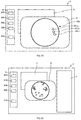
Images


Classifications
-
- H—ELECTRICITY
- H01—ELECTRIC ELEMENTS
- H01J—ELECTRIC DISCHARGE TUBES OR DISCHARGE LAMPS
- H01J37/00—Discharge tubes with provision for introducing objects or material to be exposed to the discharge, e.g. for the purpose of examination or processing thereof
- H01J37/26—Electron or ion microscopes; Electron or ion diffraction tubes
- H01J37/28—Electron or ion microscopes; Electron or ion diffraction tubes with scanning beams
-
- G—PHYSICS
- G01—MEASURING; TESTING
- G01N—INVESTIGATING OR ANALYSING MATERIALS BY DETERMINING THEIR CHEMICAL OR PHYSICAL PROPERTIES
- G01N23/00—Investigating or analysing materials by the use of wave or particle radiation, e.g. X-rays or neutrons, not covered by groups G01N3/00 – G01N17/00, G01N21/00 or G01N22/00
- G01N23/22—Investigating or analysing materials by the use of wave or particle radiation, e.g. X-rays or neutrons, not covered by groups G01N3/00 – G01N17/00, G01N21/00 or G01N22/00 by measuring secondary emission from the material
- G01N23/225—Investigating or analysing materials by the use of wave or particle radiation, e.g. X-rays or neutrons, not covered by groups G01N3/00 – G01N17/00, G01N21/00 or G01N22/00 by measuring secondary emission from the material using electron or ion
- G01N23/2251—Investigating or analysing materials by the use of wave or particle radiation, e.g. X-rays or neutrons, not covered by groups G01N3/00 – G01N17/00, G01N21/00 or G01N22/00 by measuring secondary emission from the material using electron or ion using incident electron beams, e.g. scanning electron microscopy [SEM]
-
- G—PHYSICS
- G06—COMPUTING OR CALCULATING; COUNTING
- G06F—ELECTRIC DIGITAL DATA PROCESSING
- G06F3/00—Input arrangements for transferring data to be processed into a form capable of being handled by the computer; Output arrangements for transferring data from processing unit to output unit, e.g. interface arrangements
- G06F3/01—Input arrangements or combined input and output arrangements for interaction between user and computer
- G06F3/048—Interaction techniques based on graphical user interfaces [GUI]
- G06F3/0484—Interaction techniques based on graphical user interfaces [GUI] for the control of specific functions or operations, e.g. selecting or manipulating an object, an image or a displayed text element, setting a parameter value or selecting a range
- G06F3/04845—Interaction techniques based on graphical user interfaces [GUI] for the control of specific functions or operations, e.g. selecting or manipulating an object, an image or a displayed text element, setting a parameter value or selecting a range for image manipulation, e.g. dragging, rotation, expansion or change of colour
-
- G—PHYSICS
- G06—COMPUTING OR CALCULATING; COUNTING
- G06T—IMAGE DATA PROCESSING OR GENERATION, IN GENERAL
- G06T7/00—Image analysis
- G06T7/0002—Inspection of images, e.g. flaw detection
-
- H—ELECTRICITY
- H01—ELECTRIC ELEMENTS
- H01J—ELECTRIC DISCHARGE TUBES OR DISCHARGE LAMPS
- H01J37/00—Discharge tubes with provision for introducing objects or material to be exposed to the discharge, e.g. for the purpose of examination or processing thereof
- H01J37/02—Details
- H01J37/22—Optical, image processing or photographic arrangements associated with the tube
- H01J37/222—Image processing arrangements associated with the tube
-
- H—ELECTRICITY
- H01—ELECTRIC ELEMENTS
- H01J—ELECTRIC DISCHARGE TUBES OR DISCHARGE LAMPS
- H01J37/00—Discharge tubes with provision for introducing objects or material to be exposed to the discharge, e.g. for the purpose of examination or processing thereof
- H01J37/26—Electron or ion microscopes; Electron or ion diffraction tubes
- H01J37/261—Details
- H01J37/265—Controlling the tube; circuit arrangements adapted to a particular application not otherwise provided, e.g. bright-field-dark-field illumination
-
- G—PHYSICS
- G06—COMPUTING OR CALCULATING; COUNTING
- G06T—IMAGE DATA PROCESSING OR GENERATION, IN GENERAL
- G06T2207/00—Indexing scheme for image analysis or image enhancement
- G06T2207/10—Image acquisition modality
- G06T2207/10056—Microscopic image
- G06T2207/10061—Microscopic image from scanning electron microscope
-
- H—ELECTRICITY
- H01—ELECTRIC ELEMENTS
- H01J—ELECTRIC DISCHARGE TUBES OR DISCHARGE LAMPS
- H01J2237/00—Discharge tubes exposing object to beam, e.g. for analysis treatment, etching, imaging
- H01J2237/22—Treatment of data
-
- H—ELECTRICITY
- H01—ELECTRIC ELEMENTS
- H01J—ELECTRIC DISCHARGE TUBES OR DISCHARGE LAMPS
- H01J2237/00—Discharge tubes exposing object to beam, e.g. for analysis treatment, etching, imaging
- H01J2237/245—Detection characterised by the variable being measured
- H01J2237/24571—Measurements of non-electric or non-magnetic variables
- H01J2237/24585—Other variables, e.g. energy, mass, velocity, time, temperature
-
- H—ELECTRICITY
- H01—ELECTRIC ELEMENTS
- H01J—ELECTRIC DISCHARGE TUBES OR DISCHARGE LAMPS
- H01J2237/00—Discharge tubes exposing object to beam, e.g. for analysis treatment, etching, imaging
- H01J2237/248—Components associated with the control of the tube
- H01J2237/2482—Optical means
-
- H—ELECTRICITY
- H01—ELECTRIC ELEMENTS
- H01J—ELECTRIC DISCHARGE TUBES OR DISCHARGE LAMPS
- H01J2237/00—Discharge tubes exposing object to beam, e.g. for analysis treatment, etching, imaging
- H01J2237/25—Tubes for localised analysis using electron or ion beams
- H01J2237/2505—Tubes for localised analysis using electron or ion beams characterised by their application
- H01J2237/2555—Microprobes, i.e. particle-induced X-ray spectrometry
- H01J2237/2561—Microprobes, i.e. particle-induced X-ray spectrometry electron
Definitions
- the present invention relates to a scanning electron microscope and image processing method.
- a scanning electron microscope equipped with an energy dispersive X-ray analyzer can perform elemental analysis to obtain compositional information of a sample.
- Such a scanning electron microscope may be equipped with an optical imaging device capable of optical imaging in order to derive whole images of a sample.
- patent document 1 discloses a scanning electron microscope equipped with an optical microscope for deriving optical images. In the scanning electron microscope of patent document 1, the optical microscope is used to check analysis positions.
- markers corresponding to a range of field of view of a scanning electron microscope (SEM) image can be displayed on an optical image taken by the optical microscope. Consequently, one can have a grasp of the positions on the optical image at which the SEM image has been captured.
- SEM scanning electron microscope
- Patent document 1 JP-A-63-116348
- One object associated with some aspects of the present invention is to provide a scanning electron microscope and image processing method free of the foregoing problem.
- a scanning electron microscope associated with the present invention comprises:
- the image processor section operates (i) to alter the magnification of the whole image based on instructions displayed on the display device for altering the magnification of the whole image, (ii) to cause new first markers of the same size as the first markers placed on the unaltered magnification whole image to be placed on the altered magnification whole image, and (iii) to cause new second markers of the same size as the second markers placed on the unaltered magnification whole image to be placed on the altered magnification whole image.
- the first and second markers are kept constant in size regardless of variation of the magnification of the whole image and, therefore, the user can get a grasp of the imaging positions and the analysis positions without respect to the magnification of the whole image.
- Another scanning electron microscope associated with the present invention comprises:
- the image processor section operates (i) to alter the magnification of the whole image based on instructions displayed on the display device for altering the magnification of the whole image and (ii) to cause new markers of the same size and configuration as the markers placed on the unaltered magnification whole image to be placed on the altered magnification whole image.
- the markers are not varied in size if the magnification of the whole image is altered. Therefore, one can get a grasp of the imaging positions without respect to the magnification of the whole image.
- An image processing method associated with the present invention is for use in a scanning electron microscope having an optical system for irradiating a sample with an electron beam, a detector for detecting secondary electrons or backscattered electrons emitted in response to the irradiation of the sample with the electron beam, a scanning electron microscope (SEM) image generator for generating a scanning electron microscope (SEM) image, based on an output signal from the detector, and a control section for controlling the optical system and the detector.
- SEM scanning electron microscope
- This image processing method starts with displaying markers indicative of imaging positions on a display device such that the markers are placed on a whole image of the sample.
- the magnification of the whole image is altered based on instructions displayed on the display device for altering the magnification of the whole image.
- New markers of the same size and configuration as the markers placed on the unaltered magnification whole image are placed on the altered magnification whole image.
- FIG. 1 shows the configuration of the scanning electron microscope, 100, associated with the present embodiment.
- the scanning electron microscope 100 includes an electron source 10, an optical system 20, a sample stage 30, an electron detector 40 (one example of a first detector), an X-ray detector 50 (one example of a second detector), an optical imaging device 60, a controller 70 (made of a control computer), a processor 80, a manual control unit 90, a display device 92, and a storage device 94.
- the electron source 10 produces electrons.
- the electron source 10 is an electron gun that emits an electron beam EB by accelerating electrons, which are emitted from a cathode, by means of an anode.
- the electron beam EB emitted from the electron source 10 is made to impinge on a sample S by the optical system 20.
- the optical system 20 includes condenser lenses 22, an objective lens 24, and beam deflectors 26.
- the electron beam EB emitted from the electron source 10 is focused by the condenser lenses 22.
- the diameter and dose of the electron beam EB can be controlled by the condenser lenses 22.
- the objective lens 24 is disposed immediately ahead of the sample S and operates to focus the electron beam EB.
- the objective lens 24 is configured, for example, including coils and a yoke.
- lines of magnetic force generated by the coils are confined in the yoke made of a material having a high magnetic permeability such as iron.
- a cutout (lens gap) is formed in a part of the yoke to permit the lines of magnetic force distributed at high density to leak onto the optical axis.
- the beam deflectors 26 deflect the electron beam EB in two dimensions.
- the deflectors 26 allow the electron beam EB to be scanned over the sample S.
- the sample S is placed on the sample stage 30, which can hold the sample S.
- the sample S is held to a sample holder (not shown) and placed on the sample stage 30.
- the sample stage 30 is configured including a moving mechanism for moving the sample S. By moving the sample S by the sample stage 30, the position on the sample S hit by the electron beam EB can be moved.
- the electron detector 40 is a secondary electron detector, for example, which detects secondary electrons emitted from the sample S in response to impingement of the electron beam EB on the sample S.
- the electron detector 40 produces an output signal which is sent to the controller 70.
- the output signal from the electron detector 40 is correlated to information about the position of impingement of the electron beam EB identified by the scan signal. Consequently, image data for generating a secondary electron image (one example of SEM image) can be derived.
- the electron detector 40 may be a backscattered electron detector for detecting backscattered electrons emitted from the sample S. In this case, image data for generating a backscattered electron image (one example of SEM image) can be obtained.
- the X-ray detector 50 detects X-rays emitted from the sample S when the electron beam EB impinges on the sample S.
- the X-ray detector 50 is an energy dispersive X-ray spectrometer (EDS).
- the X-ray detector 50 may be a wavelength dispersive X-ray spectrometer (WDS).
- the X-ray detector 50 produces an output signal that is sent to the controller 70.
- the optical imaging device 60 captures optical images of the sample S.
- the optical imaging device 60 is a digital camera (e.g., CCD (charge coupled device) camera or CMOS (complementary metal-oxide-semiconductor) camera).
- the optical imaging device 60 may be an optical microscope equipped with a digital camera, for example.
- the optical imaging device 60 sends the captured optical images (image data) to the controller 70.
- the controller 70 supplies control signals to control various components (e.g., the sample stage 30, electron detector 40, X-ray detector 50, and optical imaging device 60) of the scanning electron microscope 100, for controlling lens currents, scan signals, and other factors.
- various components e.g., the sample stage 30, electron detector 40, X-ray detector 50, and optical imaging device 60
- the controller 70 supplies scan signals to the beam deflectors 26 such that the electron beam EB is scanned at the imaging position specified by the control information. Consequently, the electron beam EB is scanned at the specified imaging position on the sample S. Secondary electrons or backscattered electrons emitted from the sample S are detected by the electron detector 40, whereby SEM images can be captured.
- control information for a point analysis is output from the control section 82
- the controller 70 controls the beam deflectors 26 such that the electron beam EB impinges at the analysis position specified by the control information.
- the electron beam EB is made to impinge at the specified analysis position on the sample S.
- X-rays emitted from the sample S are detected by the X-ray detector 50.
- an EDS spectrum representing analysis results can be obtained.
- the controller 70 performs processing to convert the output signal from the electron detector 40 into a signal form (image data) that can be read by the processor 80. Furthermore, the controller 70 performs processing to convert the output signal from the X-ray detector 50 into a signal form that can be read by the processor 80. In addition, the controller 70 performs processing to send the optical images (image data) from the optical imaging device 60 to the processor 80.
- the manual control unit 90 performs processing to convert instructions from the user into a control signal and to send it to the processor 80.
- the manual control unit 90 can be implemented, for example, by an input device such as buttons, keys, touch panel display, microphone, or the like.
- the manual control unit 90 can accept input of instructions, for example, for altering the magnification of the whole image of the sample S.
- the manual control unit 90 can accept input, for example, of the imaging position of an SEM image and the analysis positions of elemental analysis.
- the display device 92 outputs the image generated by the processor 80.
- the display device 92 can be realized, for example, by an LCD (liquid crystal display) or other display unit.
- Programs and data permitting the processor 80 to perform various computational operations and various control operations are stored in the storage device 94.
- the storage device 94 is also used as a working area for the processor 80.
- the storage device 94 can be realized, for example, by a RAM (random access memory), a ROM (read only memory), a hard disk, or the like.
- the processor 80 performs processing operations including operations for controlling various portions of the scanning electron microscope 100, operations for generating SEM images, operations for performing elemental analysis, and operations for generating images or graphical objects representing imaging positions and analysis positions.
- the functions of the processor 80 can be implemented by executing computer programs using various processors (e.g., central processing units (CPUs)).
- the processor 80 includes the control section 82, an SEM image generator 84, an elemental analyzer 86, and an image processor section 88.
- the control section 82 controls various portions of the scanning electron microscope 100.
- the control section 82 generates control information for controlling various portions of the microscope 100, for example, based on a control signal from the manual control unit 90. For example, if a user enters instructions for specifying the magnification of the whole image 602 via the manual control unit 90, the control section 82 generates control information in response to the instructions. Furthermore, if the user enters instructions for specifying an imaging position or analysis positions via the manual control unit 90, the control section 82 generates control information in response to the instructions. When the user enters other instructions via the manual control unit 90, the control section 82 similarly generates control information in response to the instructions.
- the SEM image generator 84 generates an SEM image based on the output signal from the electron detector 40 that represents image data.
- the elemental analyzer 86 performs elemental analysis, based on the output signal from the X-ray detector 50. For example, when a point analysis is performed, the elemental analyzer 86 generates an EDS spectrum. When a line analysis is performed, the elemental analyzer 86 generates a line profile. When an area analysis is performed, the elemental analyzer 86 generates an elemental map.
- the image processor section 88 displays the first markers and second markers indicative of imaging positions and analysis positions, respectively, on the display device 92 in such a way that the first and second markers are placed on the whole image of the sample S.
- the image processor section 88 alters the magnification of the whole image based on the instructions and causes new first markers of the same size as the first markers placed on the unaltered magnification whole image to be placed on the altered magnification whole image. Similarly, the image processor section 88 causes new second markers of the same size as the second markers placed on the unaltered magnification whole image to be placed on the altered magnification whole image.
- the image processor section 88 acquires first control information indicating imaging condition from the control section 82 and varies the color of the first markers based on the first control information. Additionally, the image processor section 88 acquires second control information indicating the condition of elemental analysis from the control section 82 and varies the color of the second markers based on the second control information.
- FIG. 2 illustrates one example of a GUI screen, 2, displayed on the display device 92.
- the GUI screen 2 includes an SEM display window 4 used for observation purposes, a whole image display window 6, and a control window 8.
- An SEM image 612 taken by the scanning electron microscope 100 is displayed in the SEM image display window 4.
- a substantially whole image 602 of the sample S is displayed in the whole image display window 6.
- Imaging positions at which the SEM image 612 is taken and analysis positions at which elemental analysis is performed using the X-ray detector 50 are displayed on the whole image of the sample S.
- the substantially whole image 602 of the sample S is an optical image of the sample S, for example, taken by the optical imaging device 60 and includes the whole of the sample S, for example.
- the substantially whole image 602 of the sample S may be an image of a part of the sample S and encompass the whole area subjected to imaging or elemental analysis.
- First markers 604, second markers 606, a third marker 608, and fourth markers 610 are displayed and superimposed on the substantially whole image 602 of the sample S.
- the first markers 604 indicate the imaging positions of the SEM image 612.
- each first marker 604 assumes the form of a flag but no restriction is imposed on the shape of the first marker 604 as long as it can indicate an imaging position.
- the first markers 604 indicative of the imaging positions vary in color according to the imaging conditions. For example, the first markers 604 are colored blue during imaging and colored red after the completion of imaging. The user may set at will the color of the first markers 604 which varies according to imaging conditions. Alternatively, the first markers 604 may blink according to the imaging conditions. For example, the first markers 604 may blink during imaging.
- the second markers 606, third marker 608, and fourth markers 610 indicate analysis positions.
- the second markers 606 indicate positions of a point analysis.
- the third marker 608 indicates a position of a line analysis.
- the fourth markers 610 indicate positions of an area analysis.
- the second markers 606 have the shape of an arrow
- the third marker 608 has the shape of a rectangle
- the fourth markers 610 have the shape of a star. No restrictions are imposed on the shapes of these markers as long as they can indicate analysis positions.
- the second markers 606, third marker 608, and fourth markers 610 are different in shape and so it is possible to visually grasp the analysis technique.
- the second markers 606 indicating analysis positions vary in color according to analysis conditions. For example, the second markers 606 are displayed in blue prior to an analysis, in yellow during the analysis, and in red after the analysis. The color of the second markers 606 which varies according to the analysis conditions may be set at will by the user.
- the second markers 606 may blink according to the analysis conditions. For example, the second markers 606 may blink during analysis.
- the third marker 608 and fourth markers 610 vary in color or blink according to the analysis conditions, in the same manner as the second markers 606.
- the taken SEM image 612 is displayed in the substantially whole image 602 of the sample S.
- the SEM image 612 is displayed at any one imaging position on the whole image 602 of the sample S in a size according to the magnification of the final image.
- the imaging magnification of the SEM image 612 is higher than the magnification of the whole image 602, the SEM image 612 will shrink to such a size that it cannot be easily visually checked on the whole image 602. In the scanning electron microscope 100, therefore, the imaging positions are indicated using the first markers 604 to permit the operator to confirm the imaging positions regardless of the final magnification of the SEM image 612.
- FIG. 3 illustrates one example of GUI screen, 2, displayed on the display device 92.
- FIG. 3 illustrates the manner in which the substantially whole image 602 of the sample S is enlarged from the state shown in FIG. 2 .
- the magnification of the whole image 602 is altered based on the instructions.
- instructions for increasing the magnification of the whole image 602 are entered and so the whole image 602 is enlarged.
- Variation of the magnification of the whole image 602 is carried out, for example, by digital zooming.
- the first markers 604 and the second markers 606 do not vary in size.
- the third marker 608 and the fourth markers 610 do not vary in size if the magnification of the whole image 602 is altered, in a manner not illustrated.
- a coordinate system for the whole image 602 of the sample S and a coordinate system for the sample stage 30 are interrelated. That is, on the whole image 602 of the sample S, the coordinates of the sample stage 30 can be uniquely determined from the coordinates of an arbitrary position to which the coordinates of the sample stage 30 correspond. Similarly, the coordinates of sample S on the whole image 602 can be uniquely determined from the coordinates of an arbitrary position on the sample stage 30 to which the former coordinates correspond.
- GUI elements (such as buttons, icons, or the like) for control and manipulation of the scanning electron microscope 100 are displayed in the control window 8.
- what are displayed in the control window 8 are an Imaging button 802, a Point analysis button 804, a Line analysis button 806, an Area analysis button 808, and a Start button 810.
- Other GUI elements for control and manipulation of the microscope 100 may also be displayed in the control window 8.
- the Imaging button 802 is a button for taking the SEM image 612.
- the SEM image 612 can be taken by moving the sample stage 30 to search for a desired field of view and depressing the Imaging button 802 at a desired position on the sample S.
- the Point analysis button 804 is used to perform a point analysis.
- An analysis position where a point analysis is performed can be specified by specifying a position on the whole image 602 of the sample S while the Point analysis button 804 is selected and activated.
- the Line analysis button 806 is used to perform a line analysis.
- An analysis position where a line analysis is performed can be specified by specifying a position on the whole image 602 of the sample S while the Line analysis button 806 is selected and activated.
- the Area analysis button 808 is used to perform an area analysis.
- An analysis position where an area analysis is performed can be specified by specifying positions or an area on the whole image 602 of the sample S while the Area analysis button 808 is selected and activated.
- the Start button 810 is used to start an analysis. For example, if the Start button 810 is depressed while an analysis position where a point analysis is performed is specified, the point analysis is initiated at the specified analysis position.
- FIGS. 4-10 illustrate the GUI screens 2.
- the optical imaging device 60 takes the whole image 602 of the sample S.
- the taken whole image 602 of the sample S is displayed in the whole image display window 6 as shown in FIG. 4 .
- the user can determine an imaging position and analysis positions, for example, by viewing the whole image 602 of the sample S displayed in the whole image display window 6.
- the SEM image 612 is taken and stored in the storage device 94.
- the first marker 604 indicative of the imaging position is shown and overlaid on the whole image 602 displayed in the whole image display window 6. During imaging the first marker 604 is displayed in blue color and after the imaging the first marker 604 is displayed in red color, for example.
- the user can search the whole image 602 displayed in the whole image display window 6 for a desired position at which an analysis is to be performed. As shown in FIG. 6 , the whole image 602 can be enlarged.
- the SEM image 612 is enlarged and shown on the whole image 602 by enlarging the whole image 602 such that the imaging position indicated by the first marker 604 is contained within the field of view.
- the first marker 604 shown in FIG. 6 and the first marker 604 shown in FIG. 5 are of the same size.
- the second markers 606 indicative of the analysis positions are placed on the SEM image 612 as shown in FIG. 6 .
- three analysis positions are specified and three second markers 606 are displayed.
- the second markers 606 are displayed in blue color prior to an analysis, displayed in yellow color during the analysis, and displayed in red color after the analysis, for example.
- the SEM image 612 is taken and the point analysis is performed.
- the first markers 604, the second markers 606, the SEM image 612, and so on are displayed and superimposed on the whole image 602 of the sample S displayed in the whole image display window 6. Accordingly, one can confirm the imaging positions and analysis positions by viewing the whole image display window 6. Line analysis and area analysis can be carried out in the same manner as the point analysis and so a description thereof is omitted.
- a result display window 9 is displayed close to the selected first marker 604.
- the imaging position is selected, for example, by clicking the first marker 604 with a mouse cursor or tapping the first marker 604 on a touch panel.
- the SEM image 612 taken at the imaging position indicated by the selected first marker 604 is displayed in the result display window 9.
- imaging conditions and so on may be displayed in the result display window 9 in a manner not illustrated.
- the result display window 9 is displayed near the selected second marker 606.
- the selection of the analysis position is done in the same way as the selection of the imaging position.
- the results of the analysis at the analysis position indicated by the selected second marker 606 are displayed in the result display window 9.
- the results of a point analysis at the analysis position indicated by the selected second marker 606, i.e., the EDS spectrum 614 are shown.
- analysis conditions, an SEM image at the analysis position, and other parameters may be displayed in the result display window 9 in a manner not illustrated.
- the image processor section 88 displays the whole image 602 of the sample S in the whole image display window 6 as shown in FIG. 4 .
- the control section 82 controls the optical system 20 and the electron detector 40 based on a control signal from the manual control unit 90 to take the SEM image 612.
- the control section 82 controls the beam deflectors 26 to scan the sample S with the electron beam EB. Consequently, secondary electrons or backscattered electrons emitted from the sample S are detected by the electron detector 40. In this way, it is possible to take the SEM image 612.
- the image processor section 88 acquires information about the imaging position from the control section 82 and places and displays the first marker 604 on the whole image 602 of the sample S so as to correspond to the imaging position on the basis of the imaging position information (see FIG. 5 ). At this time, the image processor section 88 acquires control information indicating that it is during imaging from the control section 82 and displays the first marker 604 in a color representing "during imaging" based on the control information.
- the SEM image 612 is stored in the storage device 94.
- the image processor section 88 displays the first marker 604 placed on the whole image 602 in a color representing "completion of imaging" based on control information indicating that taking of the SEM image 612 is finished.
- the image processor section 88 displays and places the second markers 606 on the whole image 602 of the sample S corresponding to the analysis positions on the basis of the entered information about the analysis positions (see FIG. 6 ). At this time, the image processor section 88 acquires control information indicating that it is "prior to analysis” from the control section 82 and displays the second markers 606 in a color indicating "prior to analysis” based on the control information.
- the control section 82 controls the optical system 20 and the X-ray detector 50 such that elemental analysis is performed at each of the analysis positions indicated by the second markers 606.
- the control section 82 controls the beam deflectors 26 such that the electron beam EB impinges at the analysis positions indicated by the second markers 606. Consequently, the X-rays emitted from the sample S are detected by the X-ray detector 50. In this way, an EDS spectrum 614 can be obtained.
- the image processor section 88 obtains control information indicating start of an analysis from the control section 82 and displays the second markers 606 placed on the whole image 602 in a color denoting "during analysis” based on the control information.
- the EDS spectrum 614 is stored in the storage device 94.
- the imager processor section 88 acquires control information indicating that the analysis has ended from the control section 82 and represents the second markers 606 placed on the whole image 602 in a color denoting "already analyzed" based on the control information.
- the image processor section 88 displays the result display window 9 near the selected first marker 604 in response to a control signal from the manual control unit 90 (see FIG. 7 ) and causes the SEM image 612 taken at the imaging position indicated by the selected first marker 604 to be displayed in the result display window 9.
- the image processor section 88 displays the result display window 9 near the selected second marker 606 in response to a control signal from the manual control unit 90 as shown in FIG. 8 and causes the results of the analysis (EDS spectrum 614) at the analysis position indicated by the selected second marker 606 to be displayed in the result display window 9.
- the image processor section 88 displays the result display window 9 near the selected marker in response to a control signal from the manual control unit 90. At this time, the image processor section 88 displays plural SEM images 612 and plural EDS spectra 614 in the result display window 9 as shown in FIG. 9 . If one of the plural imaging results and plural analysis results displayed in the single display window 9 is selected, the image processor section 88 displays the detail display window 902 for showing details of the analysis results in response to a control signal from the manual control unit 90.
- the scanning electron microscope 100 has the following features.
- the image processor section 88 alters the magnification of the whole image 602 based on instructions for altering the magnification of the whole image 602 of the sample S displayed on the display device 92 and displays new first markers 604 of the same size as the first markers 604 placed on the unaltered magnification whole image 602 such that the new first markers 604 are placed on the altered magnification whole image 602. Therefore, in the scanning electron microscope 100, if the magnification of the whole image 602 is altered, the first markers 604 do not vary in size. Consequently, it is possible to grasp the imaging position without relying on the magnification of the whole image 602.
- the image processor section 88 alters the magnification of the whole image 602 based on instructions for altering the magnification of the whole image 602 of the sample S displayed on the display device 92 and displays new second markers 606 of the same size as the second markers 606 placed on the unaltered magnification whole image 602 such that the new second markers 606 are placed on the altered magnification whole image 602. Therefore, in the scanning electron microscope 100, if the magnification of the whole image 602 is altered, the second markers 606 remain constant in size. Hence, it is possible to grasp the analysis positions without reliance on the magnification of the whole image 602.
- the image processor section 88 acquires first control information indicating imaging conditions from the control section 82 and alters the color of the first markers 604 based on the first control information. Therefore, in the scanning electron microscope 100, it is possible to easily grasp the imaging conditions.
- the image processor section 88 blinks the first markers 604 based on the first control information. Therefore, in the scanning electron microscope 100, it is easy to grasp the imaging conditions.
- the first control information indicates that it is “during imaging” or “already imaged”. Therefore, in the scanning electron microscope 100, it is possible to grasp whether the imaging position indicated by each first marker 604 is being imaged or already imaged.
- the image processor section 88 obtains second control information indicating the state of an elemental analysis from the control section 82 and alters the color of the second markers 606 based on the second control information. Therefore, in the scanning electron microscope 100, it is easy to grasp the state of the elemental analysis.
- the image processor section 88 blinks the second markers 606 based on the second control information. Therefore, in the scanning electron microscope 100, the state of the elemental analysis can be grasped easily.
- the second control information indicates “prior to analysis”, “during analysis”, or “completion of analysis”. Therefore, in the scanning electron microscope 100, the user can grasp in which one of the states “prior to analysis”, “during analysis”, and “completion of analysis” is each of the imaging positions indicated by the second markers 606.
- the scanning electron microscope 100 includes the optical imaging device 60 for optically imaging the sample S.
- the whole image 602 of the sample S is an image of the sample S captured by the optical imaging device 60. Therefore, in the scanning electron microscope 100, imaging positions and analysis positions can be indicated on an optical image of the sample S.
- the image processor section 88 causes the results of imaging done at the imaging position indicated by the first marker 604 to be displayed on the display device 92. Therefore, in the scanning electron microscope 100, the imaging position and the SEM image 612 taken at this imaging position can be intercorrelated.
- the image processor section 88 causes the results of the analysis at the analysis position indicated by the second marker 606 to be displayed on the display device 92. Therefore, in the scanning electron microscope 100, the analysis position and the results of the analysis at this analysis position can be intercorrelated.
- An image processing method associated with the present embodiment involves the steps of: causing the first markers 604 indicative of imaging positions and the second markers 606 indicative of analysis positions to be displayed on the display device 92 such that the first and second markers 604, 606 are placed on the whole image 602 of the sample S; altering the magnification of the whole image 602 based on instructions for altering the magnification of the whole image 602 displayed on the display device 92; and displaying new first markers 604 of the same size as the first markers 604 placed on the unaltered magnification whole image 602 such that the new first markers 604 are placed on the altered magnification whole image 602.
- the image processing method associated with the present embodiment further includes the step of displaying new second markers 606 of the same size as the second markers 606 placed on the unaltered magnification whole image 602 such that the new second markers 606 are placed on the altered magnification whole image 602.
- the first markers 604 and second markers 606 remain constant in size and so the imaging positions and analysis positions can be grasped regardless of the magnification of the whole image 602.
- FIG. 11 is a diagram showing the configuration of a scanning electron microscope associated with a first modified embodiment. Those members of this microscope, 200, which are similar in function to their respective counterparts of the above-described scanning electron microscope 100 are indicated by the same reference numerals as in the above referenced figures and a detail description thereof is omitted.
- the above-described scanning electron microscope 100 has the optical imaging device 60 as shown in FIG. 1 .
- the whole image 602 of the sample S is an optical image of the sample S taken by the optical imaging device 60.
- the scanning electron microscope 200 has no optical imaging device as shown in FIG. 11 .
- the whole image 602 of the sample S is a computer graphics image.
- CG images each representative of the whole image 602 of the sample S are stored in the storage device 94 in a corresponding manner to plural sample holders capable of being installed on the sample stage 30. These CG images are images of the sample holders and each represents the whole image 602 of the sample S. The user can select the CG image corresponding to the used sample holder and use it as the whole image 602 of the sample S.
- FIG. 12 illustrates one example of the GUI screen 2 displayed on the display device 92.
- analysis positions are specified on the SEM image 612 as shown in FIG. 3 .
- analysis positions can be specified directly on the whole image 602 of the sample S as shown in FIG. 12 . That is, analysis positions can be specified within an area not imaged, i.e., not contributing to the SEM image 612.
- the user can specify analysis positions on the whole image 602 of the sample S through the manual control unit 90. Consequently, elemental analysis can be performed by specifying analysis positions without taking the SEM image 612. 5.3.
- FIG. 13 illustrates one example of the GUI screen 2 displayed on the display device 92.
- the image processor section 88 may operate such that symbols 607 are displayed on the display device 92 and attached to the second markers 606 to indicate an analysis order.
- the image processor section 88 attaches the symbols 607 indicating the analysis order to the second markers 606 on the display device 92 based on the analysis order specified by the user.
- numbers “1", “2", “3", “4", and "5" are attached as the symbols 607 to the five second markers 606, respectively, to denote the analysis order. If the analysis order can be grasped, the symbols 607 are not restricted to the example shown in FIG. 13 .
- the image processor section 88 attaches symbols indicative of an analysis order to the plural second markers 606 on the display device 92. Therefore, it is easy to grasp the analysis order.
- FIG. 14 illustrates one example of the GUI screen 2 displayed on the display device 92.
- both imaging and analysis are conducted at the same position on the sample S or plural analyses are performed at the same position on the sample S.
- the shapes of markers disposed on the whole image 602 of the sample S are varied according to the combination of such imaging and analysis. For example, in the example shown in FIG. 14 , when imaging and a point analysis are performed at the same position, a triangularly shaped marker 601a is placed. When imaging and a line analysis are performed at the same position, a pentagonally shaped marker 601b is placed. When imaging, a point analysis, and an area analysis are performed at the same position, an octagonally shaped marker 601c is placed.
- the image processor section 88 alters the shapes of the markers according to the combination of imaging and analysis. Therefore, it is easy to grasp the combination of imaging and analysis.
- the image processor section 88 may vary the colors of the markers according to the combination of imaging and analysis. Also, in this case, similar effects can be produced.
- FIG. 15 illustrates one example of the GUI screen 2 displayed on the display device 92.
- the GUI screen 2 can have a history display window 7 for showing histories of imaging operations and analysis operations.
- captured SEM images and analysis results are displayed in a temporal sequence.
- the image processor section 88 displays the histories of imaging (SEM imaging) operations and elemental analysis operations on the display device 92. Therefore, it is easy to grasp the histories of imaging and elemental analysis.
- the above-described scanning electron microscope 100 shown in FIG. 1 has the X-ray detector 50 for performing elemental analysis.
- a detector for performing elemental analysis is not restricted to this type of device.
- a scanning electron microscope associated with the present invention can have an Auger electron spectroscopy analyzer as a detector for performing elemental analysis, the Auger electron spectroscopy analyzer operating to detect Auger electrons emitted from the sample S. This arrangement can yield effects similar to those produced by the above-described scanning electron microscope 100 shown in FIG. 1 .
- the present invention embraces configurations substantially identical (e.g., in function, and method) with the configurations described in the embodiments of the invention. Furthermore, the invention embraces configurations described in the embodiments and including portions which have non-essential portions replaced. Further, the invention embraces configurations which are similar to the configurations described in the embodiments except that well-known techniques have been added.
Landscapes
- Engineering & Computer Science (AREA)
- Chemical & Material Sciences (AREA)
- Analytical Chemistry (AREA)
- Computer Vision & Pattern Recognition (AREA)
- General Physics & Mathematics (AREA)
- Physics & Mathematics (AREA)
- Theoretical Computer Science (AREA)
- General Engineering & Computer Science (AREA)
- Quality & Reliability (AREA)
- General Health & Medical Sciences (AREA)
- Biochemistry (AREA)
- Immunology (AREA)
- Pathology (AREA)
- Life Sciences & Earth Sciences (AREA)
- Human Computer Interaction (AREA)
- Health & Medical Sciences (AREA)
- Analysing Materials By The Use Of Radiation (AREA)
Abstract
Description
- The present invention relates to a scanning electron microscope and image processing method.
- A scanning electron microscope equipped with an energy dispersive X-ray analyzer can perform elemental analysis to obtain compositional information of a sample.
- Such a scanning electron microscope may be equipped with an optical imaging device capable of optical imaging in order to derive whole images of a sample. For example, patent document 1 discloses a scanning electron microscope equipped with an optical microscope for deriving optical images. In the scanning electron microscope of patent document 1, the optical microscope is used to check analysis positions.
- Furthermore, in the scanning electron microscope of patent document 1, markers corresponding to a range of field of view of a scanning electron microscope (SEM) image can be displayed on an optical image taken by the optical microscope. Consequently, one can have a grasp of the positions on the optical image at which the SEM image has been captured.
- Patent document 1:
JP-A-63-116348 - With a scanning electron microscope, however, observations at high magnifications of 10,000 times and higher can be made. Therefore, in the case of the scanning electron microscope of patent document 1, if the magnification of the optical image is high, the markers may be confirmed. If the magnification of the optical image is varied to a lower magnification, the markers will be reduced in size and so the markers may not be checked. In this way, where markers corresponding to a range of field of view are displayed on an optical image, it is impossible to have a grasp of the imaging positions depending on the magnification of the optical image.
- In view of the foregoing problem, the present invention has been made. One object associated with some aspects of the present invention is to provide a scanning electron microscope and image processing method free of the foregoing problem.
- A scanning electron microscope associated with the present invention comprises:
- an optical system for irradiating a sample with an electron beam;
- a first detector for detecting secondary electrons or backscattered electrons emitted in response to the irradiation of the sample with the electron beam;
- a second detector for detecting X-rays or Auger electrons emitted in response to the irradiation of the sample with the electron beam;
- a scanning electron microscope (SEM) image generator for generating a scanning electron microscope (SEM) image, based on an output signal from the first detector;
- an elemental analyzer for performing elemental analysis based on an output signal from the second detector;
- a control section for controlling the optical system, the first detector, and the second detector; and
- an image processor section for causing first markers indicative of imaging positions and second markers indicative of analysis positions to be displayed on a display device such that the first and second markers are placed on a whole image of the sample.
- The image processor section operates (i) to alter the magnification of the whole image based on instructions displayed on the display device for altering the magnification of the whole image, (ii) to cause new first markers of the same size as the first markers placed on the unaltered magnification whole image to be placed on the altered magnification whole image, and (iii) to cause new second markers of the same size as the second markers placed on the unaltered magnification whole image to be placed on the altered magnification whole image.
- In this scanning electron microscope, the first and second markers are kept constant in size regardless of variation of the magnification of the whole image and, therefore, the user can get a grasp of the imaging positions and the analysis positions without respect to the magnification of the whole image.
- Another scanning electron microscope associated with the present invention comprises:
- an optical system for irradiating a sample with an electron beam;
- a detector for detecting secondary electrons or backscattered electrons emitted in response to the irradiation of the sample with the electron beam;
- a scanning electron microscope (SEM) image generator for generating a scanning electron microscope (SEM) image, based on an output signal from the detector;
- a control section for controlling the optical system and the detector; and
- an image processor section for displaying markers indicative of imaging positions on a display device such that the markers are placed on a whole image of the sample.
- The image processor section operates (i) to alter the magnification of the whole image based on instructions displayed on the display device for altering the magnification of the whole image and (ii) to cause new markers of the same size and configuration as the markers placed on the unaltered magnification whole image to be placed on the altered magnification whole image.
- In this scanning electron microscope, the markers are not varied in size if the magnification of the whole image is altered. Therefore, one can get a grasp of the imaging positions without respect to the magnification of the whole image.
- An image processing method associated with the present invention is for use in a scanning electron microscope having
an optical system for irradiating a sample with an electron beam,
a detector for detecting secondary electrons or backscattered electrons emitted in response to the irradiation of the sample with the electron beam,
a scanning electron microscope (SEM) image generator for generating a scanning electron microscope (SEM) image, based on an output signal from the detector, and
a control section for controlling the optical system and the detector. - This image processing method starts with displaying markers indicative of imaging positions on a display device such that the markers are placed on a whole image of the sample. The magnification of the whole image is altered based on instructions displayed on the display device for altering the magnification of the whole image. New markers of the same size and configuration as the markers placed on the unaltered magnification whole image are placed on the altered magnification whole image.
- In this image processing method, if the magnification of the whole image is altered, the markers do not change in size. Therefore, one can get a grasp of the imaging positions without relying on the magnification of the whole image.
-
-
FIG. 1 is a block diagram illustrating the configuration of a scanning electron microscope associated with one embodiment of the present invention. -
FIG. 2 illustrates one example of GUI (graphical user interface) screen displayed on the display device. -
FIG. 3 illustrates another example of GUI screen displayed on the display device. -
FIGS. 4-9 illustrate GUI screens. -
FIG. 10 illustrates manipulations using a GUI screen. -
FIG. 11 is a block diagram similar toFIG. 1 , but showing the configuration of a scanning electron microscope associated with a first modified embodiment. -
FIGS. 12-15 illustrate GUI screens displayed on the display device shown inFIG. 11 . - The preferred embodiments of the present invention are hereinafter described in detail with reference to the drawings. It is to be understood that the embodiments described below are not intended to unduly restrict the content of the present invention delineated by the appended claims and that not all the configurations described below are essential constituent components of the invention.
- A scanning electron microscope associated with one embodiment of the present invention is first described by referring to the drawings.
FIG. 1 shows the configuration of the scanning electron microscope, 100, associated with the present embodiment. As shown inFIG. 1 , thescanning electron microscope 100 includes anelectron source 10, anoptical system 20, asample stage 30, an electron detector 40 (one example of a first detector), an X-ray detector 50 (one example of a second detector), anoptical imaging device 60, a controller 70 (made of a control computer), aprocessor 80, amanual control unit 90, adisplay device 92, and astorage device 94. - The
electron source 10 produces electrons. For example, theelectron source 10 is an electron gun that emits an electron beam EB by accelerating electrons, which are emitted from a cathode, by means of an anode. - The electron beam EB emitted from the
electron source 10 is made to impinge on a sample S by theoptical system 20. Theoptical system 20 includescondenser lenses 22, anobjective lens 24, andbeam deflectors 26. - The electron beam EB emitted from the
electron source 10 is focused by thecondenser lenses 22. For example, the diameter and dose of the electron beam EB can be controlled by thecondenser lenses 22. - The
objective lens 24 is disposed immediately ahead of the sample S and operates to focus the electron beam EB. Theobjective lens 24 is configured, for example, including coils and a yoke. In theobjective lens 24, lines of magnetic force generated by the coils are confined in the yoke made of a material having a high magnetic permeability such as iron. A cutout (lens gap) is formed in a part of the yoke to permit the lines of magnetic force distributed at high density to leak onto the optical axis. - The beam deflectors 26 deflect the electron beam EB in two dimensions. The
deflectors 26 allow the electron beam EB to be scanned over the sample S. - The sample S is placed on the
sample stage 30, which can hold the sample S. For example, the sample S is held to a sample holder (not shown) and placed on thesample stage 30. Thesample stage 30 is configured including a moving mechanism for moving the sample S. By moving the sample S by thesample stage 30, the position on the sample S hit by the electron beam EB can be moved. - The
electron detector 40 is a secondary electron detector, for example, which detects secondary electrons emitted from the sample S in response to impingement of the electron beam EB on the sample S. Theelectron detector 40 produces an output signal which is sent to thecontroller 70. In thecontroller 70, the output signal from theelectron detector 40 is correlated to information about the position of impingement of the electron beam EB identified by the scan signal. Consequently, image data for generating a secondary electron image (one example of SEM image) can be derived. Alternatively, theelectron detector 40 may be a backscattered electron detector for detecting backscattered electrons emitted from the sample S. In this case, image data for generating a backscattered electron image (one example of SEM image) can be obtained. - The
X-ray detector 50 detects X-rays emitted from the sample S when the electron beam EB impinges on the sample S. For example, theX-ray detector 50 is an energy dispersive X-ray spectrometer (EDS). Alternatively, theX-ray detector 50 may be a wavelength dispersive X-ray spectrometer (WDS). TheX-ray detector 50 produces an output signal that is sent to thecontroller 70. - The
optical imaging device 60 captures optical images of the sample S. For example, theoptical imaging device 60 is a digital camera (e.g., CCD (charge coupled device) camera or CMOS (complementary metal-oxide-semiconductor) camera). Alternatively, theoptical imaging device 60 may be an optical microscope equipped with a digital camera, for example. Theoptical imaging device 60 sends the captured optical images (image data) to thecontroller 70. - Based on control information from a
control section 82, thecontroller 70 supplies control signals to control various components (e.g., thesample stage 30,electron detector 40,X-ray detector 50, and optical imaging device 60) of thescanning electron microscope 100, for controlling lens currents, scan signals, and other factors. - For example, in a case where control information for capturing SEM images is output from the
control section 82, thecontroller 70 supplies scan signals to thebeam deflectors 26 such that the electron beam EB is scanned at the imaging position specified by the control information. Consequently, the electron beam EB is scanned at the specified imaging position on the sample S. Secondary electrons or backscattered electrons emitted from the sample S are detected by theelectron detector 40, whereby SEM images can be captured. - In a case where control information for a point analysis is output from the
control section 82, thecontroller 70 controls thebeam deflectors 26 such that the electron beam EB impinges at the analysis position specified by the control information. In consequence, the electron beam EB is made to impinge at the specified analysis position on the sample S. X-rays emitted from the sample S are detected by theX-ray detector 50. As a result, an EDS spectrum representing analysis results can be obtained. - The
controller 70 performs processing to convert the output signal from theelectron detector 40 into a signal form (image data) that can be read by theprocessor 80. Furthermore, thecontroller 70 performs processing to convert the output signal from theX-ray detector 50 into a signal form that can be read by theprocessor 80. In addition, thecontroller 70 performs processing to send the optical images (image data) from theoptical imaging device 60 to theprocessor 80. - The
manual control unit 90 performs processing to convert instructions from the user into a control signal and to send it to theprocessor 80. Themanual control unit 90 can be implemented, for example, by an input device such as buttons, keys, touch panel display, microphone, or the like. Themanual control unit 90 can accept input of instructions, for example, for altering the magnification of the whole image of the sample S. Furthermore, themanual control unit 90 can accept input, for example, of the imaging position of an SEM image and the analysis positions of elemental analysis. - The
display device 92 outputs the image generated by theprocessor 80. Thedisplay device 92 can be realized, for example, by an LCD (liquid crystal display) or other display unit. - Programs and data permitting the
processor 80 to perform various computational operations and various control operations are stored in thestorage device 94. Thestorage device 94 is also used as a working area for theprocessor 80. Thestorage device 94 can be realized, for example, by a RAM (random access memory), a ROM (read only memory), a hard disk, or the like. - The
processor 80 performs processing operations including operations for controlling various portions of thescanning electron microscope 100, operations for generating SEM images, operations for performing elemental analysis, and operations for generating images or graphical objects representing imaging positions and analysis positions. The functions of theprocessor 80 can be implemented by executing computer programs using various processors (e.g., central processing units (CPUs)). Theprocessor 80 includes thecontrol section 82, anSEM image generator 84, anelemental analyzer 86, and animage processor section 88. - The
control section 82 controls various portions of thescanning electron microscope 100. Thecontrol section 82 generates control information for controlling various portions of themicroscope 100, for example, based on a control signal from themanual control unit 90. For example, if a user enters instructions for specifying the magnification of thewhole image 602 via themanual control unit 90, thecontrol section 82 generates control information in response to the instructions. Furthermore, if the user enters instructions for specifying an imaging position or analysis positions via themanual control unit 90, thecontrol section 82 generates control information in response to the instructions. When the user enters other instructions via themanual control unit 90, thecontrol section 82 similarly generates control information in response to the instructions. - The
SEM image generator 84 generates an SEM image based on the output signal from theelectron detector 40 that represents image data. Theelemental analyzer 86 performs elemental analysis, based on the output signal from theX-ray detector 50. For example, when a point analysis is performed, theelemental analyzer 86 generates an EDS spectrum. When a line analysis is performed, theelemental analyzer 86 generates a line profile. When an area analysis is performed, theelemental analyzer 86 generates an elemental map. - The
image processor section 88 displays the first markers and second markers indicative of imaging positions and analysis positions, respectively, on thedisplay device 92 in such a way that the first and second markers are placed on the whole image of the sample S. - When instructions for altering the magnification of the whole image of the sample S displayed on the
display device 92 are entered, theimage processor section 88 alters the magnification of the whole image based on the instructions and causes new first markers of the same size as the first markers placed on the unaltered magnification whole image to be placed on the altered magnification whole image. Similarly, theimage processor section 88 causes new second markers of the same size as the second markers placed on the unaltered magnification whole image to be placed on the altered magnification whole image. - Furthermore, the
image processor section 88 acquires first control information indicating imaging condition from thecontrol section 82 and varies the color of the first markers based on the first control information. Additionally, theimage processor section 88 acquires second control information indicating the condition of elemental analysis from thecontrol section 82 and varies the color of the second markers based on the second control information. - The technique of the present embodiment is next described with reference to some drawings.
FIG. 2 illustrates one example of a GUI screen, 2, displayed on thedisplay device 92. As shown inFIG. 2 , theGUI screen 2 includes anSEM display window 4 used for observation purposes, a wholeimage display window 6, and acontrol window 8. - An
SEM image 612 taken by thescanning electron microscope 100 is displayed in the SEMimage display window 4. A substantiallywhole image 602 of the sample S is displayed in the wholeimage display window 6. Imaging positions at which theSEM image 612 is taken and analysis positions at which elemental analysis is performed using theX-ray detector 50 are displayed on the whole image of the sample S. - The substantially
whole image 602 of the sample S is an optical image of the sample S, for example, taken by theoptical imaging device 60 and includes the whole of the sample S, for example. Alternatively, the substantiallywhole image 602 of the sample S may be an image of a part of the sample S and encompass the whole area subjected to imaging or elemental analysis. -
First markers 604,second markers 606, athird marker 608, andfourth markers 610 are displayed and superimposed on the substantiallywhole image 602 of the sample S. - The
first markers 604 indicate the imaging positions of theSEM image 612. In the illustrated example, eachfirst marker 604 assumes the form of a flag but no restriction is imposed on the shape of thefirst marker 604 as long as it can indicate an imaging position. - The
first markers 604 indicative of the imaging positions vary in color according to the imaging conditions. For example, thefirst markers 604 are colored blue during imaging and colored red after the completion of imaging. The user may set at will the color of thefirst markers 604 which varies according to imaging conditions. Alternatively, thefirst markers 604 may blink according to the imaging conditions. For example, thefirst markers 604 may blink during imaging. - The
second markers 606,third marker 608, andfourth markers 610 indicate analysis positions. Thesecond markers 606 indicate positions of a point analysis. Thethird marker 608 indicates a position of a line analysis. Thefourth markers 610 indicate positions of an area analysis. In the illustrated example, thesecond markers 606 have the shape of an arrow, thethird marker 608 has the shape of a rectangle, and thefourth markers 610 have the shape of a star. No restrictions are imposed on the shapes of these markers as long as they can indicate analysis positions. Thesecond markers 606,third marker 608, andfourth markers 610 are different in shape and so it is possible to visually grasp the analysis technique. - The
second markers 606 indicating analysis positions vary in color according to analysis conditions. For example, thesecond markers 606 are displayed in blue prior to an analysis, in yellow during the analysis, and in red after the analysis. The color of thesecond markers 606 which varies according to the analysis conditions may be set at will by the user. Thesecond markers 606 may blink according to the analysis conditions. For example, thesecond markers 606 may blink during analysis. Thethird marker 608 andfourth markers 610 vary in color or blink according to the analysis conditions, in the same manner as thesecond markers 606. - The taken
SEM image 612, for example, is displayed in the substantiallywhole image 602 of the sample S. TheSEM image 612 is displayed at any one imaging position on thewhole image 602 of the sample S in a size according to the magnification of the final image. - Where the imaging magnification of the
SEM image 612 is higher than the magnification of thewhole image 602, theSEM image 612 will shrink to such a size that it cannot be easily visually checked on thewhole image 602. In thescanning electron microscope 100, therefore, the imaging positions are indicated using thefirst markers 604 to permit the operator to confirm the imaging positions regardless of the final magnification of theSEM image 612. -
FIG. 3 illustrates one example of GUI screen, 2, displayed on thedisplay device 92.FIG. 3 illustrates the manner in which the substantiallywhole image 602 of the sample S is enlarged from the state shown inFIG. 2 . - When the user enters instructions for altering the magnification of the
whole image 602 through themanual control unit 90, the magnification of thewhole image 602 is altered based on the instructions. In the example shown inFIG. 3 , instructions for increasing the magnification of thewhole image 602 are entered and so thewhole image 602 is enlarged. Variation of the magnification of thewhole image 602 is carried out, for example, by digital zooming. - If the magnification of the
whole image 602 is altered, thefirst markers 604 and thesecond markers 606 do not vary in size. Similarly, thethird marker 608 and thefourth markers 610 do not vary in size if the magnification of thewhole image 602 is altered, in a manner not illustrated. - A coordinate system for the
whole image 602 of the sample S and a coordinate system for thesample stage 30 are interrelated. That is, on thewhole image 602 of the sample S, the coordinates of thesample stage 30 can be uniquely determined from the coordinates of an arbitrary position to which the coordinates of thesample stage 30 correspond. Similarly, the coordinates of sample S on thewhole image 602 can be uniquely determined from the coordinates of an arbitrary position on thesample stage 30 to which the former coordinates correspond. - GUI elements (such as buttons, icons, or the like) for control and manipulation of the
scanning electron microscope 100 are displayed in thecontrol window 8. In particular, what are displayed in thecontrol window 8 are anImaging button 802, aPoint analysis button 804, aLine analysis button 806, anArea analysis button 808, and aStart button 810. Other GUI elements for control and manipulation of themicroscope 100 may also be displayed in thecontrol window 8. - The
Imaging button 802 is a button for taking theSEM image 612. TheSEM image 612 can be taken by moving thesample stage 30 to search for a desired field of view and depressing theImaging button 802 at a desired position on the sample S. - The
Point analysis button 804 is used to perform a point analysis. An analysis position where a point analysis is performed can be specified by specifying a position on thewhole image 602 of the sample S while thePoint analysis button 804 is selected and activated. - The
Line analysis button 806 is used to perform a line analysis. An analysis position where a line analysis is performed can be specified by specifying a position on thewhole image 602 of the sample S while theLine analysis button 806 is selected and activated. - The
Area analysis button 808 is used to perform an area analysis. An analysis position where an area analysis is performed can be specified by specifying positions or an area on thewhole image 602 of the sample S while theArea analysis button 808 is selected and activated. - The
Start button 810 is used to start an analysis. For example, if theStart button 810 is depressed while an analysis position where a point analysis is performed is specified, the point analysis is initiated at the specified analysis position. -
FIGS. 4-10 illustrate the GUI screens 2. - When a user enters instructions for taking the substantially
whole image 602 of the sample S through themanual control unit 90, theoptical imaging device 60 takes thewhole image 602 of the sample S. The takenwhole image 602 of the sample S is displayed in the wholeimage display window 6 as shown inFIG. 4 . The user can determine an imaging position and analysis positions, for example, by viewing thewhole image 602 of the sample S displayed in the wholeimage display window 6. - When the user determines an imaging position and enters instructions for taking the
SEM image 612 through themanual control unit 90, theSEM image 612 is taken and stored in thestorage device 94. As shown inFIG. 5 , thefirst marker 604 indicative of the imaging position is shown and overlaid on thewhole image 602 displayed in the wholeimage display window 6. During imaging thefirst marker 604 is displayed in blue color and after the imaging thefirst marker 604 is displayed in red color, for example. - The user can search the
whole image 602 displayed in the wholeimage display window 6 for a desired position at which an analysis is to be performed. As shown inFIG. 6 , thewhole image 602 can be enlarged. TheSEM image 612 is enlarged and shown on thewhole image 602 by enlarging thewhole image 602 such that the imaging position indicated by thefirst marker 604 is contained within the field of view. - As shown in
FIG. 6 , although thewhole image 602 of the sample S is enlarged as compared to thewhole image 602 of the sample S shown inFIG. 5 , thefirst marker 604 shown inFIG. 6 and thefirst marker 604 shown inFIG. 5 are of the same size. - When the user enters instructions for specifying analysis positions on the taken
SEM image 612 through themanual control unit 90, thesecond markers 606 indicative of the analysis positions are placed on theSEM image 612 as shown inFIG. 6 . In the example shown inFIG. 6 , three analysis positions are specified and threesecond markers 606 are displayed. Thesecond markers 606 are displayed in blue color prior to an analysis, displayed in yellow color during the analysis, and displayed in red color after the analysis, for example. - When the user enters instructions for starting an analysis through the
manual control unit 90, a point analysis is performed at each of the analysis positions indicated by thesecond markers 606. As a result, an EDS spectrum 614 (seeFIG. 8 ) is obtained and stored in thestorage device 94. - As described above, the
SEM image 612 is taken and the point analysis is performed. Thefirst markers 604, thesecond markers 606, theSEM image 612, and so on are displayed and superimposed on thewhole image 602 of the sample S displayed in the wholeimage display window 6. Accordingly, one can confirm the imaging positions and analysis positions by viewing the wholeimage display window 6. Line analysis and area analysis can be carried out in the same manner as the point analysis and so a description thereof is omitted. - As shown in
FIG. 7 , when the user selects thefirst marker 604 indicative of a desired imaging position through themanual control unit 90, aresult display window 9 is displayed close to the selectedfirst marker 604. The imaging position is selected, for example, by clicking thefirst marker 604 with a mouse cursor or tapping thefirst marker 604 on a touch panel. TheSEM image 612 taken at the imaging position indicated by the selectedfirst marker 604 is displayed in theresult display window 9. Furthermore, imaging conditions and so on may be displayed in theresult display window 9 in a manner not illustrated. - As shown in
FIG. 8 , when the user selects onesecond marker 606 indicative of an analysis position through themanual control unit 90, theresult display window 9 is displayed near the selectedsecond marker 606. The selection of the analysis position is done in the same way as the selection of the imaging position. The results of the analysis at the analysis position indicated by the selectedsecond marker 606 are displayed in theresult display window 9. In the example shown inFIG. 8 , the results of a point analysis at the analysis position indicated by the selectedsecond marker 606, i.e., theEDS spectrum 614, are shown. In addition, analysis conditions, an SEM image at the analysis position, and other parameters may be displayed in theresult display window 9 in a manner not illustrated. - When plural imaging operations and plural analyses are performed at the same position, if the marker located at this same position is selected,
plural SEM images 612 andplural EDS spectra 614 are displayed in theresult display window 9 as shown inFIG. 9 . If one of the imaging results and analysis results displayed in the singleresult display windows 9 is selected, adetail display window 902 for showing analysis results in detail is displayed as shown inFIG. 10 . Length measurement, spectral analysis, editing of an elemental map, and so on can be done in thedetail display window 902. - The processing performed by the
processor 80 is next described. - When the
whole image 602 of the sample S is taken using theoptical imaging device 60, theimage processor section 88 displays thewhole image 602 of the sample S in the wholeimage display window 6 as shown inFIG. 4 . - The
control section 82 controls theoptical system 20 and theelectron detector 40 based on a control signal from themanual control unit 90 to take theSEM image 612. In particular, thecontrol section 82 controls thebeam deflectors 26 to scan the sample S with the electron beam EB. Consequently, secondary electrons or backscattered electrons emitted from the sample S are detected by theelectron detector 40. In this way, it is possible to take theSEM image 612. - The
image processor section 88 acquires information about the imaging position from thecontrol section 82 and places and displays thefirst marker 604 on thewhole image 602 of the sample S so as to correspond to the imaging position on the basis of the imaging position information (seeFIG. 5 ). At this time, theimage processor section 88 acquires control information indicating that it is during imaging from thecontrol section 82 and displays thefirst marker 604 in a color representing "during imaging" based on the control information. - When the taking of the
SEM image 612 is completed, theSEM image 612 is stored in thestorage device 94. Theimage processor section 88 displays thefirst marker 604 placed on thewhole image 602 in a color representing "completion of imaging" based on control information indicating that taking of theSEM image 612 is finished. - When the user enters instructions for specifying analysis positions through the
manual control unit 90, theimage processor section 88 displays and places thesecond markers 606 on thewhole image 602 of the sample S corresponding to the analysis positions on the basis of the entered information about the analysis positions (seeFIG. 6 ). At this time, theimage processor section 88 acquires control information indicating that it is "prior to analysis" from thecontrol section 82 and displays thesecond markers 606 in a color indicating "prior to analysis" based on the control information. - The
control section 82 controls theoptical system 20 and theX-ray detector 50 such that elemental analysis is performed at each of the analysis positions indicated by thesecond markers 606. In particular, thecontrol section 82 controls thebeam deflectors 26 such that the electron beam EB impinges at the analysis positions indicated by thesecond markers 606. Consequently, the X-rays emitted from the sample S are detected by theX-ray detector 50. In this way, anEDS spectrum 614 can be obtained. - When a point analysis at each analysis position is initiated, the
image processor section 88 obtains control information indicating start of an analysis from thecontrol section 82 and displays thesecond markers 606 placed on thewhole image 602 in a color denoting "during analysis" based on the control information. - When the analysis at the analysis position ends, the
EDS spectrum 614 is stored in thestorage device 94. Theimager processor section 88 acquires control information indicating that the analysis has ended from thecontrol section 82 and represents thesecond markers 606 placed on thewhole image 602 in a color denoting "already analyzed" based on the control information. - When the user selects the
first marker 604 indicative of the imaging position through themanual control unit 90, theimage processor section 88 displays theresult display window 9 near the selectedfirst marker 604 in response to a control signal from the manual control unit 90 (seeFIG. 7 ) and causes theSEM image 612 taken at the imaging position indicated by the selectedfirst marker 604 to be displayed in theresult display window 9. - When the user selects one
second marker 606 indicative of an analysis position through themanual control unit 90, theimage processor section 88 displays theresult display window 9 near the selectedsecond marker 606 in response to a control signal from themanual control unit 90 as shown inFIG. 8 and causes the results of the analysis (EDS spectrum 614) at the analysis position indicated by the selectedsecond marker 606 to be displayed in theresult display window 9. - When plural imaging operations and plural analyses are conducted at the same position, if the marker placed at this same position is selected, the
image processor section 88 displays theresult display window 9 near the selected marker in response to a control signal from themanual control unit 90. At this time, theimage processor section 88 displaysplural SEM images 612 andplural EDS spectra 614 in theresult display window 9 as shown inFIG. 9 . If one of the plural imaging results and plural analysis results displayed in thesingle display window 9 is selected, theimage processor section 88 displays thedetail display window 902 for showing details of the analysis results in response to a control signal from themanual control unit 90. - The
scanning electron microscope 100 has the following features. In thescanning electron microscope 100, theimage processor section 88 alters the magnification of thewhole image 602 based on instructions for altering the magnification of thewhole image 602 of the sample S displayed on thedisplay device 92 and displays newfirst markers 604 of the same size as thefirst markers 604 placed on the unaltered magnificationwhole image 602 such that the newfirst markers 604 are placed on the altered magnificationwhole image 602. Therefore, in thescanning electron microscope 100, if the magnification of thewhole image 602 is altered, thefirst markers 604 do not vary in size. Consequently, it is possible to grasp the imaging position without relying on the magnification of thewhole image 602. - Furthermore, in the
scanning electron microscope 100, theimage processor section 88 alters the magnification of thewhole image 602 based on instructions for altering the magnification of thewhole image 602 of the sample S displayed on thedisplay device 92 and displays newsecond markers 606 of the same size as thesecond markers 606 placed on the unaltered magnificationwhole image 602 such that the newsecond markers 606 are placed on the altered magnificationwhole image 602. Therefore, in thescanning electron microscope 100, if the magnification of thewhole image 602 is altered, thesecond markers 606 remain constant in size. Hence, it is possible to grasp the analysis positions without reliance on the magnification of thewhole image 602. - In the
scanning electron microscope 100, theimage processor section 88 acquires first control information indicating imaging conditions from thecontrol section 82 and alters the color of thefirst markers 604 based on the first control information. Therefore, in thescanning electron microscope 100, it is possible to easily grasp the imaging conditions. - In the
scanning electron microscope 100, theimage processor section 88 blinks thefirst markers 604 based on the first control information. Therefore, in thescanning electron microscope 100, it is easy to grasp the imaging conditions. - In the
scanning electron microscope 100, the first control information indicates that it is "during imaging" or "already imaged". Therefore, in thescanning electron microscope 100, it is possible to grasp whether the imaging position indicated by eachfirst marker 604 is being imaged or already imaged. - In the
scanning electron microscope 100, theimage processor section 88 obtains second control information indicating the state of an elemental analysis from thecontrol section 82 and alters the color of thesecond markers 606 based on the second control information. Therefore, in thescanning electron microscope 100, it is easy to grasp the state of the elemental analysis. - In the
scanning electron microscope 100, theimage processor section 88 blinks thesecond markers 606 based on the second control information. Therefore, in thescanning electron microscope 100, the state of the elemental analysis can be grasped easily. - In the
scanning electron microscope 100, the second control information indicates "prior to analysis", "during analysis", or "completion of analysis". Therefore, in thescanning electron microscope 100, the user can grasp in which one of the states "prior to analysis", "during analysis", and "completion of analysis" is each of the imaging positions indicated by thesecond markers 606. - The
scanning electron microscope 100 includes theoptical imaging device 60 for optically imaging the sample S. Thewhole image 602 of the sample S is an image of the sample S captured by theoptical imaging device 60. Therefore, in thescanning electron microscope 100, imaging positions and analysis positions can be indicated on an optical image of the sample S. - In the
scanning electron microscope 100, if onefirst marker 604 placed on thewhole image 602 of the sample S is selected, theimage processor section 88 causes the results of imaging done at the imaging position indicated by thefirst marker 604 to be displayed on thedisplay device 92. Therefore, in thescanning electron microscope 100, the imaging position and theSEM image 612 taken at this imaging position can be intercorrelated. - In the
scanning electron microscope 100, if one of thesecond markers 606 placed on thewhole image 602 of the sample S is selected, theimage processor section 88 causes the results of the analysis at the analysis position indicated by thesecond marker 606 to be displayed on thedisplay device 92. Therefore, in thescanning electron microscope 100, the analysis position and the results of the analysis at this analysis position can be intercorrelated. - An image processing method associated with the present embodiment involves the steps of: causing the
first markers 604 indicative of imaging positions and thesecond markers 606 indicative of analysis positions to be displayed on thedisplay device 92 such that the first andsecond markers whole image 602 of the sample S; altering the magnification of thewhole image 602 based on instructions for altering the magnification of thewhole image 602 displayed on thedisplay device 92; and displaying newfirst markers 604 of the same size as thefirst markers 604 placed on the unaltered magnificationwhole image 602 such that the newfirst markers 604 are placed on the altered magnificationwhole image 602. The image processing method associated with the present embodiment further includes the step of displaying newsecond markers 606 of the same size as thesecond markers 606 placed on the unaltered magnificationwhole image 602 such that the newsecond markers 606 are placed on the altered magnificationwhole image 602. - Therefore, in the image processing method associated with the present embodiment, if the magnification of the
whole image 602 is altered, thefirst markers 604 andsecond markers 606 remain constant in size and so the imaging positions and analysis positions can be grasped regardless of the magnification of thewhole image 602. - It is to be understood that the present invention is not restricted to the above embodiment but rather can be practiced in variously modified forms without departing from the gist of the invention. In the following, only differences with the above-described
scanning electron microscope 100 are described; a description of similarities is omitted. 5.1. First Modified Embodiment -
FIG. 11 is a diagram showing the configuration of a scanning electron microscope associated with a first modified embodiment. Those members of this microscope, 200, which are similar in function to their respective counterparts of the above-describedscanning electron microscope 100 are indicated by the same reference numerals as in the above referenced figures and a detail description thereof is omitted. - The above-described
scanning electron microscope 100 has theoptical imaging device 60 as shown inFIG. 1 . Thewhole image 602 of the sample S is an optical image of the sample S taken by theoptical imaging device 60. - On the other hand, the
scanning electron microscope 200 has no optical imaging device as shown inFIG. 11 . Thewhole image 602 of the sample S is a computer graphics image. - Plural computer graphics (CG) images each representative of the
whole image 602 of the sample S are stored in thestorage device 94 in a corresponding manner to plural sample holders capable of being installed on thesample stage 30. These CG images are images of the sample holders and each represents thewhole image 602 of the sample S. The user can select the CG image corresponding to the used sample holder and use it as thewhole image 602 of the sample S. -
FIG. 12 illustrates one example of theGUI screen 2 displayed on thedisplay device 92. - With the above-described
scanning electron microscope 100, analysis positions are specified on theSEM image 612 as shown inFIG. 3 . Alternatively, analysis positions can be specified directly on thewhole image 602 of the sample S as shown inFIG. 12 . That is, analysis positions can be specified within an area not imaged, i.e., not contributing to theSEM image 612. - For example, the user can specify analysis positions on the
whole image 602 of the sample S through themanual control unit 90. Consequently, elemental analysis can be performed by specifying analysis positions without taking theSEM image 612. 5.3. Third Modified Embodiment -
FIG. 13 illustrates one example of theGUI screen 2 displayed on thedisplay device 92. As shown inFIG. 13 , when the pluralsecond markers 606 are placed on thewhole image 602 of the sample S, theimage processor section 88 may operate such thatsymbols 607 are displayed on thedisplay device 92 and attached to thesecond markers 606 to indicate an analysis order. - When the user enters an analysis order through the
manual control unit 90, theimage processor section 88 attaches thesymbols 607 indicating the analysis order to thesecond markers 606 on thedisplay device 92 based on the analysis order specified by the user. In the example shown inFIG. 13 , numbers "1", "2", "3", "4", and "5" are attached as thesymbols 607 to the fivesecond markers 606, respectively, to denote the analysis order. If the analysis order can be grasped, thesymbols 607 are not restricted to the example shown inFIG. 13 . - In the third modified embodiment, the
image processor section 88 attaches symbols indicative of an analysis order to the pluralsecond markers 606 on thedisplay device 92. Therefore, it is easy to grasp the analysis order. -
FIG. 14 illustrates one example of theGUI screen 2 displayed on thedisplay device 92. Sometimes, both imaging and analysis are conducted at the same position on the sample S or plural analyses are performed at the same position on the sample S. In a fourth modified embodiment, the shapes of markers disposed on thewhole image 602 of the sample S are varied according to the combination of such imaging and analysis. For example, in the example shown inFIG. 14 , when imaging and a point analysis are performed at the same position, a triangularly shapedmarker 601a is placed. When imaging and a line analysis are performed at the same position, a pentagonally shapedmarker 601b is placed. When imaging, a point analysis, and an area analysis are performed at the same position, an octagonallyshaped marker 601c is placed. - In the fourth modified embodiment, the
image processor section 88 alters the shapes of the markers according to the combination of imaging and analysis. Therefore, it is easy to grasp the combination of imaging and analysis. Alternatively, theimage processor section 88 may vary the colors of the markers according to the combination of imaging and analysis. Also, in this case, similar effects can be produced. -
FIG. 15 illustrates one example of theGUI screen 2 displayed on thedisplay device 92. As shown inFIG. 15 , theGUI screen 2 can have a history display window 7 for showing histories of imaging operations and analysis operations. In the history display window 7, captured SEM images and analysis results are displayed in a temporal sequence. - In the fifth modified embodiment, the
image processor section 88 displays the histories of imaging (SEM imaging) operations and elemental analysis operations on thedisplay device 92. Therefore, it is easy to grasp the histories of imaging and elemental analysis. - The above-described
scanning electron microscope 100 shown inFIG. 1 has theX-ray detector 50 for performing elemental analysis. A detector for performing elemental analysis is not restricted to this type of device. A scanning electron microscope associated with the present invention can have an Auger electron spectroscopy analyzer as a detector for performing elemental analysis, the Auger electron spectroscopy analyzer operating to detect Auger electrons emitted from the sample S. This arrangement can yield effects similar to those produced by the above-describedscanning electron microscope 100 shown inFIG. 1 . - It is to be noted that the above embodiments and modifications are merely exemplary and that the invention is not restricted thereto. For example, the embodiments and modifications may be combined appropriately.
- The present invention embraces configurations substantially identical (e.g., in function, and method) with the configurations described in the embodiments of the invention. Furthermore, the invention embraces configurations described in the embodiments and including portions which have non-essential portions replaced. Further, the invention embraces configurations which are similar to the configurations described in the embodiments except that well-known techniques have been added.
Claims (15)
- A scanning electron microscope comprising:an optical system for irradiating a sample with an electron beam;a first detector for detecting secondary electrons or backscattered electrons emitted in response to the irradiation of the sample with the electron beam;a second detector for detecting X-rays or Auger electrons emitted in response to the irradiation of the sample with the electron beam;a scanning electron microscope (SEM) image generator for generating a scanning electron microscope (SEM) image, based on an output signal from the first detector;an elemental analyzer for performing elemental analysis based on an output signal from the second detector;a control section for controlling the optical system, the first detector, and the second detector; andan image processor section for causing first markers indicative of imaging positions and second markers indicative of analysis positions to be displayed on a display device such that the first and second markers are placed on a whole image of the sample;wherein the image processor section operates to alter the magnification of the whole image based on instructions displayed on the display device for altering the magnification of the whole image, to cause new first markers of the same size as the first markers placed on the unaltered magnification whole image to be placed on the altered magnification whole image, and to cause new second markers of the same size as the second markers placed on the unaltered magnification whole image to be placed on the altered magnification whole image.
- A scanning electron microscope as set forth in claim 1, wherein said image processor section acquires first control information indicating imaging conditions from said control section and alters the color of the first markers based on the first control information.
- A scanning electron microscope as set forth in claim 2, wherein said image processor section blinks said first markers based on said first control information.
- A scanning electron microscope as set forth in any one of claims 2 and 3, wherein said first control information indicates whether it is during imaging or it is after the completion of imaging.
- A scanning electron microscope as set forth in any one of claims 1 to 4, wherein said image processor section acquires second control information indicating conditions of elemental analysis from said control section and alters the color of said second markers based on the second control information.
- A scanning electron microscope as set forth in claim 5, wherein said image processor section blinks said second markers based on said second control information.
- A scanning electron microscope as set forth in any one of claims 5 and 6, wherein said second control information indicates whether it is prior to analysis, it is during analysis, or it is after the completion of analysis.
- A scanning electron microscope as set forth in any one of claims 1 to 7, wherein said second markers are placed on said whole image, and wherein said image processor section operates such that symbols indicative of an analysis order are displayed on the display device and attached to the second markers.
- A scanning electron microscope as set forth in any one of claims 1 to 8, wherein there is further provided an optical imaging device for optically imaging said sample, and wherein said whole image is an image of the sample taken by the optical imaging device.
- A scanning electron microscope as set forth in any one of claims 1 to 8, wherein said whole image is a computer graphics image.
- A scanning electron microscope as set forth in any one of claims 1 to 10, wherein, when any one of the first markers placed on said whole image is selected, said image processor section causes results of imaging done at the imaging position indicated by the selected first marker to be displayed on said display device.
- A scanning electron microscope as set forth in any one of claims 1 to 11, wherein, when any one of the second markers placed on said whole image is selected, said image processor section causes results of analysis performed at the analysis position indicated by the selected second marker to be displayed on said display device.
- A scanning electron microscope as set forth in any one of claims 1 to 12, wherein said control section controls said optical system and said second detector to perform analysis at said analysis positions indicated by said second markers.
- A scanning electron microscope comprising:an optical system for irradiating a sample with an electron beam;a detector for detecting secondary electrons or backscattered electrons emitted in response to the irradiation of the sample with the electron beam;a scanning electron microscope (SEM) image generator for generating a scanning electron microscope (SEM) image, based on an output signal from the detector;a control section for controlling the optical system and the detector; andan image processor section for displaying markers indicative of imaging positions on a display device such that the markers are placed on a whole image of the sample;wherein the image processor section operates to alter the magnification of the whole image based on instructions displayed on the display device for altering the magnification of the whole image and to cause new markers of the same size and configuration as the markers placed on the unaltered magnification whole image to be placed on the altered magnification whole image.
- An image processing method for use in a scanning electron microscope having
an optical system for irradiating a sample with an electron beam,
a detector for detecting secondary electrons or backscattered electron emitted in response to the irradiation of the sample with the electron beam,
a scanning electron microscope (SEM) image generator for generating a scanning electron microscope (SEM) image, based on an output signal from the detector, and
a control section for controlling the optical system and the detector, said image processing method comprising the steps of:displaying markers indicative of imaging positions on a display device such that the markers are placed on a whole image of the sample;altering the magnification of the whole image based on instructions displayed on the display device for altering the magnification of the whole image; andcausing new markers of the same size and configuration as the markers placed on the unaltered magnification whole image to be placed on the altered magnification whole image.
Applications Claiming Priority (1)
| Application Number | Priority Date | Filing Date | Title |
|---|---|---|---|
| JP2018214674A JP6901460B2 (en) | 2018-11-15 | 2018-11-15 | Scanning electron microscope and image processing method |
Publications (3)
| Publication Number | Publication Date |
|---|---|
| EP3654360A2 true EP3654360A2 (en) | 2020-05-20 |
| EP3654360A3 EP3654360A3 (en) | 2020-06-17 |
| EP3654360B1 EP3654360B1 (en) | 2025-01-01 |
Family
ID=68583164
Family Applications (1)
| Application Number | Title | Priority Date | Filing Date |
|---|---|---|---|
| EP19209394.6A Active EP3654360B1 (en) | 2018-11-15 | 2019-11-15 | Scanning electron microscope and image processing method |
Country Status (3)
| Country | Link |
|---|---|
| US (1) | US10964510B2 (en) |
| EP (1) | EP3654360B1 (en) |
| JP (1) | JP6901460B2 (en) |
Cited By (1)
| Publication number | Priority date | Publication date | Assignee | Title |
|---|---|---|---|---|
| DE102020102502A1 (en) | 2020-01-31 | 2021-08-05 | Carl Zeiss Microscopy Gmbh | Process, particle beam system and computer program product for energy dispersive X-ray spectroscopy |
Families Citing this family (4)
| Publication number | Priority date | Publication date | Assignee | Title |
|---|---|---|---|---|
| US12354830B2 (en) * | 2019-09-04 | 2025-07-08 | Hitachi High-Tech Corporation | Sample image display system and charged particle beam apparatus |
| CN112630242B (en) * | 2020-12-03 | 2023-01-10 | 成都先进金属材料产业技术研究院股份有限公司 | Navigation method for scanning electron microscope sample |
| JP7807560B2 (en) * | 2022-09-06 | 2026-01-27 | 株式会社日立ハイテク | Observation support device |
| CN121359236A (en) * | 2023-07-05 | 2026-01-16 | 株式会社日立高新技术 | Observation auxiliary device |
Citations (1)
| Publication number | Priority date | Publication date | Assignee | Title |
|---|---|---|---|---|
| JPS63116348A (en) | 1986-10-31 | 1988-05-20 | Jeol Ltd | View matching device of electron beam device |
Family Cites Families (7)
| Publication number | Priority date | Publication date | Assignee | Title |
|---|---|---|---|---|
| JPS6271864U (en) * | 1985-10-25 | 1987-05-08 | ||
| JPH09184715A (en) * | 1995-12-28 | 1997-07-15 | Hitachi Ltd | Pattern shape inspection device |
| US7738693B2 (en) * | 2002-12-24 | 2010-06-15 | Lam Research Corporation | User interface for wafer data analysis and visualization |
| JP2009087280A (en) * | 2007-10-03 | 2009-04-23 | Ict Solutions:Kk | Map information display system, terminal device, application server, and map information display program |
| EP2450936B1 (en) | 2010-11-03 | 2013-03-13 | Carl Zeiss NTS Ltd. | Microscope system, method for operating a charged-particle microscope |
| US10410338B2 (en) * | 2013-11-04 | 2019-09-10 | Kla-Tencor Corporation | Method and system for correlating optical images with scanning electron microscopy images |
| JP2018100867A (en) * | 2016-12-20 | 2018-06-28 | パイオニア株式会社 | Display device, control method, program, and storage medium |
-
2018
- 2018-11-15 JP JP2018214674A patent/JP6901460B2/en active Active
-
2019
- 2019-11-13 US US16/682,369 patent/US10964510B2/en active Active
- 2019-11-15 EP EP19209394.6A patent/EP3654360B1/en active Active
Patent Citations (1)
| Publication number | Priority date | Publication date | Assignee | Title |
|---|---|---|---|---|
| JPS63116348A (en) | 1986-10-31 | 1988-05-20 | Jeol Ltd | View matching device of electron beam device |
Cited By (1)
| Publication number | Priority date | Publication date | Assignee | Title |
|---|---|---|---|---|
| DE102020102502A1 (en) | 2020-01-31 | 2021-08-05 | Carl Zeiss Microscopy Gmbh | Process, particle beam system and computer program product for energy dispersive X-ray spectroscopy |
Also Published As
| Publication number | Publication date |
|---|---|
| US10964510B2 (en) | 2021-03-30 |
| JP2020087513A (en) | 2020-06-04 |
| EP3654360B1 (en) | 2025-01-01 |
| EP3654360A3 (en) | 2020-06-17 |
| JP6901460B2 (en) | 2021-07-14 |
| US20200161087A1 (en) | 2020-05-21 |
Similar Documents
| Publication | Publication Date | Title |
|---|---|---|
| EP3654360B1 (en) | Scanning electron microscope and image processing method | |
| JP5715873B2 (en) | Defect classification method and defect classification system | |
| JP3888980B2 (en) | Material identification system | |
| JP4399471B2 (en) | Transmission electron microscope with electron spectrometer | |
| EP3327749B1 (en) | Scanning transmission electron microscope and method of image generation | |
| JP2019027938A (en) | Image processing device for realizing material informatics | |
| CN112394076A (en) | Method for examining a sample using a charged particle microscope | |
| US6774362B2 (en) | Analytical method for electron microscopy | |
| WO2016121009A1 (en) | Charged particle beam device | |
| CN108292578B (en) | Charged particle beam device, observation method using charged particle beam device, and program | |
| JP7198360B2 (en) | Charged particle beam device | |
| US9859092B2 (en) | Particle beam microscope and method for operating a particle beam microscope | |
| CN114270182B (en) | Charged particle beam device | |
| JP2018190622A (en) | Electron microscope and control method | |
| JP4413887B2 (en) | Material identification system | |
| JP2003098129A (en) | Energy dispersive micro analyzer | |
| US11495432B2 (en) | Charged particle beam device and method for controlling sample stage | |
| JP3041353B2 (en) | Charged particle beam scanning type image display | |
| CN111146062A (en) | Electron microscope and image processing method | |
| JP2026002425A (en) | Charged particle beam device and image generation method | |
| JPH10282060A (en) | Mass spectrometer | |
| CN119678240A (en) | Observation aids | |
| JP2014049214A (en) | Electron microscope and acquisition method of electron microscope image | |
| JP2014149923A (en) | Charged particle beam device | |
| CN113203762A (en) | Method of energy dispersing X-ray spectra, particle beam system and computer program product |
Legal Events
| Date | Code | Title | Description |
|---|---|---|---|
| PUAI | Public reference made under article 153(3) epc to a published international application that has entered the european phase |
Free format text: ORIGINAL CODE: 0009012 |
|
| STAA | Information on the status of an ep patent application or granted ep patent |
Free format text: STATUS: THE APPLICATION HAS BEEN PUBLISHED |
|
| PUAL | Search report despatched |
Free format text: ORIGINAL CODE: 0009013 |
|
| AK | Designated contracting states |
Kind code of ref document: A2 Designated state(s): AL AT BE BG CH CY CZ DE DK EE ES FI FR GB GR HR HU IE IS IT LI LT LU LV MC MK MT NL NO PL PT RO RS SE SI SK SM TR |
|
| AX | Request for extension of the european patent |
Extension state: BA ME |
|
| AK | Designated contracting states |
Kind code of ref document: A3 Designated state(s): AL AT BE BG CH CY CZ DE DK EE ES FI FR GB GR HR HU IE IS IT LI LT LU LV MC MK MT NL NO PL PT RO RS SE SI SK SM TR |
|
| AX | Request for extension of the european patent |
Extension state: BA ME |
|
| RIC1 | Information provided on ipc code assigned before grant |
Ipc: H01J 37/26 20060101ALI20200508BHEP Ipc: H01J 37/28 20060101ALI20200508BHEP Ipc: H01J 37/22 20060101AFI20200508BHEP |
|
| STAA | Information on the status of an ep patent application or granted ep patent |
Free format text: STATUS: REQUEST FOR EXAMINATION WAS MADE |
|
| 17P | Request for examination filed |
Effective date: 20200911 |
|
| RBV | Designated contracting states (corrected) |
Designated state(s): AL AT BE BG CH CY CZ DE DK EE ES FI FR GB GR HR HU IE IS IT LI LT LU LV MC MK MT NL NO PL PT RO RS SE SI SK SM TR |
|
| STAA | Information on the status of an ep patent application or granted ep patent |
Free format text: STATUS: EXAMINATION IS IN PROGRESS |
|
| 17Q | First examination report despatched |
Effective date: 20240228 |
|
| GRAP | Despatch of communication of intention to grant a patent |
Free format text: ORIGINAL CODE: EPIDOSNIGR1 |
|
| STAA | Information on the status of an ep patent application or granted ep patent |
Free format text: STATUS: GRANT OF PATENT IS INTENDED |
|
| RIC1 | Information provided on ipc code assigned before grant |
Ipc: G06F 3/04845 20220101ALI20240711BHEP Ipc: G01N 23/2251 20180101ALI20240711BHEP Ipc: H01J 37/28 20060101ALI20240711BHEP Ipc: H01J 37/26 20060101ALI20240711BHEP Ipc: H01J 37/22 20060101AFI20240711BHEP |
|
| INTG | Intention to grant announced |
Effective date: 20240806 |
|
| GRAS | Grant fee paid |
Free format text: ORIGINAL CODE: EPIDOSNIGR3 |
|
| GRAA | (expected) grant |
Free format text: ORIGINAL CODE: 0009210 |
|
| STAA | Information on the status of an ep patent application or granted ep patent |
Free format text: STATUS: THE PATENT HAS BEEN GRANTED |
|
| RAP3 | Party data changed (applicant data changed or rights of an application transferred) |
Owner name: JEOL LTD. |
|
| AK | Designated contracting states |
Kind code of ref document: B1 Designated state(s): AL AT BE BG CH CY CZ DE DK EE ES FI FR GB GR HR HU IE IS IT LI LT LU LV MC MK MT NL NO PL PT RO RS SE SI SK SM TR |
|
| REG | Reference to a national code |
Ref country code: GB Ref legal event code: FG4D |
|
| REG | Reference to a national code |
Ref country code: CH Ref legal event code: EP |
|
| REG | Reference to a national code |
Ref country code: DE Ref legal event code: R096 Ref document number: 602019064197 Country of ref document: DE |
|
| REG | Reference to a national code |
Ref country code: IE Ref legal event code: FG4D |
|
| REG | Reference to a national code |
Ref country code: LT Ref legal event code: MG9D |
|
| REG | Reference to a national code |
Ref country code: NL Ref legal event code: MP Effective date: 20250101 |
|
| REG | Reference to a national code |
Ref country code: AT Ref legal event code: MK05 Ref document number: 1757190 Country of ref document: AT Kind code of ref document: T Effective date: 20250101 |
|
| PG25 | Lapsed in a contracting state [announced via postgrant information from national office to epo] |
Ref country code: NL Free format text: LAPSE BECAUSE OF FAILURE TO SUBMIT A TRANSLATION OF THE DESCRIPTION OR TO PAY THE FEE WITHIN THE PRESCRIBED TIME-LIMIT Effective date: 20250101 |
|
| PG25 | Lapsed in a contracting state [announced via postgrant information from national office to epo] |
Ref country code: FI Free format text: LAPSE BECAUSE OF FAILURE TO SUBMIT A TRANSLATION OF THE DESCRIPTION OR TO PAY THE FEE WITHIN THE PRESCRIBED TIME-LIMIT Effective date: 20250101 |
|
| PG25 | Lapsed in a contracting state [announced via postgrant information from national office to epo] |
Ref country code: PL Free format text: LAPSE BECAUSE OF FAILURE TO SUBMIT A TRANSLATION OF THE DESCRIPTION OR TO PAY THE FEE WITHIN THE PRESCRIBED TIME-LIMIT Effective date: 20250101 |
|
| PG25 | Lapsed in a contracting state [announced via postgrant information from national office to epo] |
Ref country code: ES Free format text: LAPSE BECAUSE OF FAILURE TO SUBMIT A TRANSLATION OF THE DESCRIPTION OR TO PAY THE FEE WITHIN THE PRESCRIBED TIME-LIMIT Effective date: 20250101 |
|
| PG25 | Lapsed in a contracting state [announced via postgrant information from national office to epo] |
Ref country code: NO Free format text: LAPSE BECAUSE OF FAILURE TO SUBMIT A TRANSLATION OF THE DESCRIPTION OR TO PAY THE FEE WITHIN THE PRESCRIBED TIME-LIMIT Effective date: 20250401 Ref country code: IS Free format text: LAPSE BECAUSE OF FAILURE TO SUBMIT A TRANSLATION OF THE DESCRIPTION OR TO PAY THE FEE WITHIN THE PRESCRIBED TIME-LIMIT Effective date: 20250501 |
|
| PG25 | Lapsed in a contracting state [announced via postgrant information from national office to epo] |
Ref country code: HR Free format text: LAPSE BECAUSE OF FAILURE TO SUBMIT A TRANSLATION OF THE DESCRIPTION OR TO PAY THE FEE WITHIN THE PRESCRIBED TIME-LIMIT Effective date: 20250101 |
|
| PG25 | Lapsed in a contracting state [announced via postgrant information from national office to epo] |
Ref country code: PT Free format text: LAPSE BECAUSE OF FAILURE TO SUBMIT A TRANSLATION OF THE DESCRIPTION OR TO PAY THE FEE WITHIN THE PRESCRIBED TIME-LIMIT Effective date: 20250502 Ref country code: LV Free format text: LAPSE BECAUSE OF FAILURE TO SUBMIT A TRANSLATION OF THE DESCRIPTION OR TO PAY THE FEE WITHIN THE PRESCRIBED TIME-LIMIT Effective date: 20250101 |
|
| PG25 | Lapsed in a contracting state [announced via postgrant information from national office to epo] |
Ref country code: BG Free format text: LAPSE BECAUSE OF FAILURE TO SUBMIT A TRANSLATION OF THE DESCRIPTION OR TO PAY THE FEE WITHIN THE PRESCRIBED TIME-LIMIT Effective date: 20250101 Ref country code: GR Free format text: LAPSE BECAUSE OF FAILURE TO SUBMIT A TRANSLATION OF THE DESCRIPTION OR TO PAY THE FEE WITHIN THE PRESCRIBED TIME-LIMIT Effective date: 20250402 |
|
| PG25 | Lapsed in a contracting state [announced via postgrant information from national office to epo] |
Ref country code: AT Free format text: LAPSE BECAUSE OF FAILURE TO SUBMIT A TRANSLATION OF THE DESCRIPTION OR TO PAY THE FEE WITHIN THE PRESCRIBED TIME-LIMIT Effective date: 20250101 |
|
| PG25 | Lapsed in a contracting state [announced via postgrant information from national office to epo] |
Ref country code: CZ Free format text: LAPSE BECAUSE OF FAILURE TO SUBMIT A TRANSLATION OF THE DESCRIPTION OR TO PAY THE FEE WITHIN THE PRESCRIBED TIME-LIMIT Effective date: 20250101 |
|
| PG25 | Lapsed in a contracting state [announced via postgrant information from national office to epo] |
Ref country code: SE Free format text: LAPSE BECAUSE OF FAILURE TO SUBMIT A TRANSLATION OF THE DESCRIPTION OR TO PAY THE FEE WITHIN THE PRESCRIBED TIME-LIMIT Effective date: 20250101 |
|
| REG | Reference to a national code |
Ref country code: DE Ref legal event code: R097 Ref document number: 602019064197 Country of ref document: DE |
|
| PG25 | Lapsed in a contracting state [announced via postgrant information from national office to epo] |
Ref country code: SM Free format text: LAPSE BECAUSE OF FAILURE TO SUBMIT A TRANSLATION OF THE DESCRIPTION OR TO PAY THE FEE WITHIN THE PRESCRIBED TIME-LIMIT Effective date: 20250101 |
|
| PG25 | Lapsed in a contracting state [announced via postgrant information from national office to epo] |
Ref country code: DK Free format text: LAPSE BECAUSE OF FAILURE TO SUBMIT A TRANSLATION OF THE DESCRIPTION OR TO PAY THE FEE WITHIN THE PRESCRIBED TIME-LIMIT Effective date: 20250101 |
|
| PG25 | Lapsed in a contracting state [announced via postgrant information from national office to epo] |
Ref country code: IT Free format text: LAPSE BECAUSE OF FAILURE TO SUBMIT A TRANSLATION OF THE DESCRIPTION OR TO PAY THE FEE WITHIN THE PRESCRIBED TIME-LIMIT Effective date: 20250101 |
|
| PG25 | Lapsed in a contracting state [announced via postgrant information from national office to epo] |
Ref country code: EE Free format text: LAPSE BECAUSE OF FAILURE TO SUBMIT A TRANSLATION OF THE DESCRIPTION OR TO PAY THE FEE WITHIN THE PRESCRIBED TIME-LIMIT Effective date: 20250101 |
|
| PG25 | Lapsed in a contracting state [announced via postgrant information from national office to epo] |
Ref country code: RO Free format text: LAPSE BECAUSE OF FAILURE TO SUBMIT A TRANSLATION OF THE DESCRIPTION OR TO PAY THE FEE WITHIN THE PRESCRIBED TIME-LIMIT Effective date: 20250101 |
|
| PG25 | Lapsed in a contracting state [announced via postgrant information from national office to epo] |
Ref country code: SK Free format text: LAPSE BECAUSE OF FAILURE TO SUBMIT A TRANSLATION OF THE DESCRIPTION OR TO PAY THE FEE WITHIN THE PRESCRIBED TIME-LIMIT Effective date: 20250101 |
|
| PLBE | No opposition filed within time limit |
Free format text: ORIGINAL CODE: 0009261 |
|
| STAA | Information on the status of an ep patent application or granted ep patent |
Free format text: STATUS: NO OPPOSITION FILED WITHIN TIME LIMIT |
|
| 26N | No opposition filed |
Effective date: 20251002 |
|
| PGFP | Annual fee paid to national office [announced via postgrant information from national office to epo] |
Ref country code: DE Payment date: 20251119 Year of fee payment: 7 |