EP3654183A1 - Information processing apparatus and method of controlling information processing apparatus - Google Patents
Information processing apparatus and method of controlling information processing apparatus Download PDFInfo
- Publication number
- EP3654183A1 EP3654183A1 EP19207699.0A EP19207699A EP3654183A1 EP 3654183 A1 EP3654183 A1 EP 3654183A1 EP 19207699 A EP19207699 A EP 19207699A EP 3654183 A1 EP3654183 A1 EP 3654183A1
- Authority
- EP
- European Patent Office
- Prior art keywords
- program
- cpu
- memory
- alteration
- executed
- Prior art date
- Legal status (The legal status is an assumption and is not a legal conclusion. Google has not performed a legal analysis and makes no representation as to the accuracy of the status listed.)
- Granted
Links
Images



Classifications
-
- G—PHYSICS
- G06—COMPUTING OR CALCULATING; COUNTING
- G06F—ELECTRIC DIGITAL DATA PROCESSING
- G06F9/00—Arrangements for program control, e.g. control units
- G06F9/06—Arrangements for program control, e.g. control units using stored programs, i.e. using an internal store of processing equipment to receive or retain programs
- G06F9/46—Multiprogramming arrangements
- G06F9/48—Program initiating; Program switching, e.g. by interrupt
- G06F9/4806—Task transfer initiation or dispatching
-
- G—PHYSICS
- G06—COMPUTING OR CALCULATING; COUNTING
- G06F—ELECTRIC DIGITAL DATA PROCESSING
- G06F21/00—Security arrangements for protecting computers, components thereof, programs or data against unauthorised activity
- G06F21/50—Monitoring users, programs or devices to maintain the integrity of platforms, e.g. of processors, firmware or operating systems
- G06F21/51—Monitoring users, programs or devices to maintain the integrity of platforms, e.g. of processors, firmware or operating systems at application loading time, e.g. accepting, rejecting, starting or inhibiting executable software based on integrity or source reliability
-
- G—PHYSICS
- G06—COMPUTING OR CALCULATING; COUNTING
- G06F—ELECTRIC DIGITAL DATA PROCESSING
- G06F12/00—Accessing, addressing or allocating within memory systems or architectures
- G06F12/14—Protection against unauthorised use of memory or access to memory
- G06F12/1408—Protection against unauthorised use of memory or access to memory by using cryptography
-
- G—PHYSICS
- G06—COMPUTING OR CALCULATING; COUNTING
- G06F—ELECTRIC DIGITAL DATA PROCESSING
- G06F12/00—Accessing, addressing or allocating within memory systems or architectures
- G06F12/14—Protection against unauthorised use of memory or access to memory
- G06F12/1458—Protection against unauthorised use of memory or access to memory by checking the subject access rights
- G06F12/1491—Protection against unauthorised use of memory or access to memory by checking the subject access rights in a hierarchical protection system, e.g. privilege levels, memory rings
-
- G—PHYSICS
- G06—COMPUTING OR CALCULATING; COUNTING
- G06F—ELECTRIC DIGITAL DATA PROCESSING
- G06F21/00—Security arrangements for protecting computers, components thereof, programs or data against unauthorised activity
- G06F21/50—Monitoring users, programs or devices to maintain the integrity of platforms, e.g. of processors, firmware or operating systems
- G06F21/52—Monitoring users, programs or devices to maintain the integrity of platforms, e.g. of processors, firmware or operating systems during program execution, e.g. stack integrity ; Preventing unwanted data erasure; Buffer overflow
- G06F21/53—Monitoring users, programs or devices to maintain the integrity of platforms, e.g. of processors, firmware or operating systems during program execution, e.g. stack integrity ; Preventing unwanted data erasure; Buffer overflow by executing in a restricted environment, e.g. sandbox or secure virtual machine
-
- G—PHYSICS
- G06—COMPUTING OR CALCULATING; COUNTING
- G06F—ELECTRIC DIGITAL DATA PROCESSING
- G06F21/00—Security arrangements for protecting computers, components thereof, programs or data against unauthorised activity
- G06F21/50—Monitoring users, programs or devices to maintain the integrity of platforms, e.g. of processors, firmware or operating systems
- G06F21/57—Certifying or maintaining trusted computer platforms, e.g. secure boots or power-downs, version controls, system software checks, secure updates or assessing vulnerabilities
- G06F21/575—Secure boot
-
- G—PHYSICS
- G06—COMPUTING OR CALCULATING; COUNTING
- G06F—ELECTRIC DIGITAL DATA PROCESSING
- G06F2221/00—Indexing scheme relating to security arrangements for protecting computers, components thereof, programs or data against unauthorised activity
- G06F2221/21—Indexing scheme relating to G06F21/00 and subgroups addressing additional information or applications relating to security arrangements for protecting computers, components thereof, programs or data against unauthorised activity
- G06F2221/2107—File encryption
-
- Y—GENERAL TAGGING OF NEW TECHNOLOGICAL DEVELOPMENTS; GENERAL TAGGING OF CROSS-SECTIONAL TECHNOLOGIES SPANNING OVER SEVERAL SECTIONS OF THE IPC; TECHNICAL SUBJECTS COVERED BY FORMER USPC CROSS-REFERENCE ART COLLECTIONS [XRACs] AND DIGESTS
- Y02—TECHNOLOGIES OR APPLICATIONS FOR MITIGATION OR ADAPTATION AGAINST CLIMATE CHANGE
- Y02D—CLIMATE CHANGE MITIGATION TECHNOLOGIES IN INFORMATION AND COMMUNICATION TECHNOLOGIES [ICT], I.E. INFORMATION AND COMMUNICATION TECHNOLOGIES AIMING AT THE REDUCTION OF THEIR OWN ENERGY USE
- Y02D10/00—Energy efficient computing, e.g. low power processors, power management or thermal management
Definitions
- the present disclosure relates to an information processing apparatus and a method of controlling the information processing apparatus.
- WO 2009-013825 discusses a method in which a CPU different from a CPU that is to execute an activation program verifies whether the activation program is altered, because the CPU that is to execute the activation program cannot detect an alteration in the activation program.
- an information processing apparatus today In response to social demands for more advanced performance, an information processing apparatus today generally includes a plurality of CPUs to execute a plurality of types of processing simultaneously and smoothly, and each CPU executes a different processing program from those executed by the other CPUs.
- an information processing apparatus includes a function of verifying whether an activation program is altered
- one of a plurality of CPUs of the information processing apparatus is to be caused to execute an alteration verification program on the activation program besides a processing program that the CPU originally executes.
- an operation program is controlled in such a manner that the CPU that is to execute the alteration verification program first executes the alteration verification program and, after the verification is completed, the CPU is switched to execute the processing program.
- an information processing apparatus as specified in claims 1 to 8.
- a method of processing information in an information processing apparatus as specified in claim 9.
- MFP multi-function peripheral
- Fig. 1 is a block diagram illustrating a MFP 100 according to a first exemplary embodiment.
- a system-on-chip (SOC) 20 includes modules 101 to 114 configured to control the MFP 100 as described below.
- a central processing unit (CPU) 101 is a processor that executes various software programs of the MFP 100 and performs various types of control of the MFP 100.
- a CPU 102 is a processor that executes an alteration detection software program and another application program that is different from the programs that are executed by the CPU 101, and performs alteration detection on the MFP 100 and controls some of applications.
- a read-only memory (ROM) 103 stores a fixed parameter of the MFP 100. Further, the ROM 103 stores the alteration detection software program and a public key described below.
- the ROM 103 is a mask ROM including a logic circuit so as not to permit writing from an external interface (I/F) or a one-time programmable (OTP) ROM that permits writing only once at the time of manufacture.
- a random access memory (RAM) 104 (volatile storage medium) is used to store a program and temporary data when the CPUs 101 and 102 control the MFP 100.
- a hard disk drive (HDD) control unit 105 performs control to read and write data from and to an HDD 115 (non-volatile storage medium). For example, the HDD control unit 105 can write image data stored in the RAM 104 to the HDD 115 via a system bus 114 and stores the image data in the HDD 115.
- a flash memory control unit 106 performs control to read and write data from and to a flash memory 116. At the time of activation, the flash memory control unit 106 can read a program stored in the flash memory 116 and develops the read program to the RAM 104 via the system bus 114.
- a network I/F control unit 107 controls data transmission and reception to and from another device and a server on a network 117.
- An external port control unit 108 is an input/output port control unit of the SOC 20.
- the external port control unit 108 optionally may control an output port so that a light-emitting diode (LED) 118 is turned on to externally provide a notification of an abnormality in the software and hardware.
- LED light-emitting diode
- a scanner I/F control unit 109 controls document reading performed by a scanner 119.
- a printer I/F control unit 110 controls printing processing performed by a printer 120.
- An image processing unit 111 is a processing unit that performs shading correction on image data read from the scanner 119 and performs halftone processing and smoothing processing to output processed data to output to the printer 120.
- a panel control unit 112 controls an operation panel 121, which is a touch panel, and controls a display of various types of information and input of a user instruction.
- a reset vector control unit 113 is a control unit that changes a setting of a reset vector (address value that is referred to after a reset state is cancelled in order to read a program to be executed after a power source is turned on) of the CPU 102, and includes a resister. The CPU 101 sets a resister setting of the reset vector control unit 113.
- the system bus 114 connects the connected modules to one another. Control signals from the CPUs 101 and 102 and data signals between the devices are transmitted and received via the system bus 114.
- the HDD 115 is a hard disk drive to store some of applications and various types of data.
- the flash memory 116 stores a basic input/output system (BIOS), a bootloader, a kernel, and an application.
- BIOS basic input/output system
- the HDD 115 and the flash memory 116 can be the same storage module.
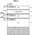
- Fig. 2 illustrates an example of a memory address map (logic address map) of the storage units as viewed from the CPU 102.
- an address area of the ROM 103 is assigned from an address 0x00000, and an address area of the flash memory 116 is assigned from an address 0x01000. Further, an address area of the RAM 104 is assigned from an address 0x10000, and an address area of the HDD 115 is assigned from an address 0x20000.
- programs 201 to 203 are to be executed by the CPU 102, and reset vectors 204 to 206 are reference destinations (address values) where the programs 201 to 203 are stored and to which the CPU 102 first refers after activation.
- the program 201 is the alteration verification program that the CPU 102 first executes.
- the program 201 is stored from the address value 0x00000 specified by the reset vector 204 of the address area of the ROM 103.
- the program 202 is the other processing program that the CPU 102 executes after the verification is completed.
- the program 202 is stored from the address value 0x01000 specified by the reset vector 205 of the address area of the flash memory 116.
- the other processing program to be executed by the CPU 102 is, for example, a processing program for performing sleep control (control to change to a normal state/sleep state) on the CPU 101 to reduce power consumption of the MFP 100 or an image processing program. In a case in which the CPU 101 satisfies a condition for changing to the sleep state, the other processing program is executed.
- the program 203 is an altered processing program that is stored in advance by an altering person (who wants to alter a program) so that the CPU 102 executes the program 203 after the verification is completed.
- the program 203 is stored from the address value 0x02000 specified by the reset vector 206 of the address area of the HDD 115.
- the reset vector of the CPU 102 is supposed to be set first to the reset vector 204, where the alteration verification program (program 201) is stored, and then to the reset vector 205, where the other processing program (program 202) is stored, after the verification is completed.
- the reset vector setting of the CPU 102 is set by changing a resister value of the reset vector control unit 113 by the operation program of the CPU 101, if the operation program of the CPU 101 is altered, the reset vector setting may be changed by the altering person.
- the reset vector may be switched to an address of an unaltered processing program stored in the HDD 115 or the RAM 104 other than the altered program 203.
- Fig. 3 is a flowchart illustrating a program to be operated by the CPU 102 immediately after the MFP 100 is turned on and a program switching sequence according to the first exemplary embodiment.
- each module in the MFP 100 is reset, and then in step S301, only the reset state of the CPU 102 is cancelled so that the CPU 102 is activated.
- the control to reset the modules in the MFP 100 is performed by, for example, switching a logic of a reset signal to be supplied to the modules at a desired timing using a reset control integrated circuit (IC).
- IC reset control integrated circuit
- the CPU 102 After the reset state of the CPU 102 is cancelled, the CPU 102 is activated so as to read the program stored in the address area specified by the reset vectors 204 to 206 and execute the read program.
- the reset vectors 204 to 206 of the CPU 102 are set to the reset vector 204, which specifies the address area of the ROM 103. Accordingly, in step S302, the CPU 102 is activated in a state where the CPU 102 reads the program 201, which is the alteration detection program and is stored in the ROM 103 that is the address area specified by the reset vector 204, and operates according to the program 201.
- step S303 the CPU 102 operating based on the alteration detection program verifies whether the program stored in the flash memory 116 is altered.
- the program on which the alteration verification is performed in step S303 is a program to be executed at the time of activation of the CPU 101.
- step S303 the program stored in the flash memory 116 is read to the RAM 104, and whether the read program is altered is verified.
- step S303 the program 202 stored in the flash memory 116 can be read to the RAM 104.
- alteration verification a case in which whether there is an alteration is verified (hereinafter, "alteration verification") using a digital signature (hereinafter, “signature”) to which a commonly-used public key cryptography method is applied will be described below as an example.
- signature a digital signature
- an alteration verification program using something other than the digital signature can also be employed.
- Signature data is a hash value calculated using a hash function with respect to a portion of a program or the entire program to be executed by the CPU 101, and the signature data is stored in advance together with a public key, which is one of a pair of encryption keys, in the ROM 103 at the timing of product shipment.
- the program to be executed by the CPU 101 is stored together with the signature data in the flash memory 116, which is rewritable by a ROM writer, because the program may be rewritten later by software update.
- the signature data stored in the flash memory 116 is externally accessed, so that the signature data is encrypted using a private key, which is the other one of the pair of encryption keys.
- the CPU 102 operating based on the program 201 which is the alteration detection program, first reads the encrypted signature data stored in the flash memory 116 and stores the read signature data in the RAM 104. Next, the CPU 102 decodes the encrypted signature data using the public key stored in the ROM 103. Then, the CPU 102 compares the decoded signature data and the signature data stored in advance in the ROM 103 to verify whether the signature data is altered.
- step S304 the CPU 102 compares the decoded signature data and the stored signature data, and in a case where there is even a small difference, the CPU 102 determines that "the program is altered", whereas in a case where the decoded signature data and the stored signature data match, the CPU 102 determines that "the program is not altered".
- step S304 determines that "the program is altered" in step S304 (YES in step S304)
- step S305 the CPU 102 performs alteration detection notification processing.
- the MFP 100 controls the output port to be supplied to the LED 118 via the external port control unit 108 to turn on the LED 118 as an external notification of the presence of the alteration.
- step S306 the reset state of the CPU 101 is cancelled.
- the reset state of the CPU 101 is cancelled by switching the logic of the reset signal to be supplied to the CPU 101 to a value that indicates "cancel".
- step S307 after the reset state of the CPU 101 is cancelled, the CPU 101 reads the program stored in the address area specified by the reset vector of the flash memory 116 (as the reset vector of the CPU 101 remains unchanged) and develops the read program to the RAM 104. Then, the CPU 101 after the reset state is cancelled executes the program developed to the RAM 104 to perform processing to activate the CPU 101.
- the reset vector setting of the CPU 102 is set by the program to be executed by the CPU 101, which is an alteration verification target. If the reset vector setting of the CPU 102 is altered, the signature data stored in the flash memory 116 becomes different from the signature data stored in the ROM 103, which is a correct value, so that the alteration of the reset vector is detected.
- step S308 the CPU 101 resets the CPU 102 based on the read program having undergone the alteration verification.
- the CPU 102 is reset by switching the logic of the reset signal to be supplied to the CPU 101 to a value that indicates "reset".
- step S309 the CPU 101 switches the reset vectors 204 to 206 of the CPU 102 to the reset vector 205 based on the program having undergone the alteration verification.
- a resister setting value of the reset vector control unit 113 that specifies the reset vector 205 is programmed as the reset vector of the CPU 102. Accordingly, the reset vector 205 is set to the CPU 102 by setting the resister value to the resister of the reset vector control unit 113.
- step S310 the CPU 101 switches the logic of the reset signal of the CPU 102 and cancels the reset state of the CPU 102 so that the CPU 102 is re-activated.
- the CPU 102 After the reset state of the CPU 102 is cancelled, the CPU 102 reads the program stored in the address area specified by the reset vector 205 and is activated so as to execute the read program.
- the RAM 104 which is the address area specified by the reset vector 205, stores the other processing program different from the alteration detection program to be executed by the CPU 102.
- the other processing program to be executed by the CPU 102 is stored in the flash memory 116 at the time immediately after the MFP 100 is turned on.
- the other processing program to be executed by the CPU 102 is stored in advance in the RAM 104, which is faster in access speed, by the CPU 101 operating based on the program having undergone the alteration verification.
- step S311 the CPU 102 reads the program 202, which is the other processing program and is stored in the RAM 104, which is the address area specified by the reset vector 205, and the CPU 102 is activated in a state of operating based on the program 202, which is the other processing program.
- the MFP 100 performs control in such a manner that at the time of switching the program to be operated by the CPU 102, the CPU 101 operating based on the program having undergone the alteration verification switches the reset vectors 204 to 206 of the CPU 102.
- the CPU 102 reads the program stored in the address area specified by the reset vector having undergone the alteration verification, and is activated. This reduces the possibility that the reset vector setting is altered by an altering person and the CPU 102 is activated from the address area storing the altered program to execute the altered program.
- control is performed in such a manner that the CPU 101 operating based on the program having undergone the alteration verification switches the reset vector of the CPU 102 to switch the program to be operated by the CPU 102 to the other processing program.
- the alteration verification is also performed on the other processing program (program 202), which is to be executed by the CPU 102 and is stored in the flash memory 116, in order to address the above-described issue.
- program 202 which is to be executed by the CPU 102 and is stored in the flash memory 116.
- An MFP according to the second exemplary embodiment will be described below as an example.
- a module or processing alike that of the MFP according to the first exemplary embodiment is given the same reference numeral, and description thereof is omitted.
- Fig. 4 is a flowchart illustrating a program to be operated by the CPU 102 immediately after the MFP 100 is turned on and a program switching sequence according to the second exemplary embodiment.
- steps S301 and S302 are alike those in the flowchart (in Fig. 3 ) according to the first exemplary embodiment, so that description thereof is omitted.
- step S403 when the CPU 102 is activated in a state of operating based on the alteration detection program, the CPU 102 verifies whether the program that is stored in the flash memory 116 and is to be operated by the CPU 101 and the other processing program that is to be executed by the CPU 102 are altered.
- Signature data of the other processing program (program 202) to be operated by the CPU 102 is also stored in advance in the ROM 103 besides the signature data of the program to be operated by the CPU 101.
- encrypted signature data of the other processing program (program 202) to be operated by the CPU 102 is stored in advance in the flash memory 116 besides the encrypted signature data of the program to be operated by the CPU 101.
- the CPU 102 operating based on the alteration detection program (program 201) first decodes the encrypted signature data of the program to be operated by the CPU 101, which is stored in the flash memory 116. Then, the CPU 102 verifies whether the program to be operated by the CPU 101 is altered, by checking whether the decoded signature data matches the signature data of the program to be operated by the CPU 101, which is stored in the ROM 103.
- the CPU 102 decodes the encrypted signature data of the other processing program (program 202) to be operated by the CPU 102, which is stored in the flash memory 116. Then, the CPU 102 verifies whether the other processing program (program 202) to be operated by the CPU 102 is altered, by checking whether the decoded signature data matches the signature data of the other processing program (program 202), which is stored in the ROM 103.
- steps S304 to S311 are alike those in the flowchart (in Fig. 3 ) according to the first exemplary embodiment, so that description thereof is omitted.
- the MFP 100 performs control in such a manner that the CPU 102 operates based on the program 202, which is the other processing program having undergone the alteration verification.
- the alteration verification can be performed on the program 202 at the time of switching the program to be executed by the CPU 102 to the other processing program (program 202).
- Embodiment(s) can also be realized by a computer of a system or apparatus that reads out and executes computer executable instructions (e.g., one or more programs) recorded on a storage medium (which may also be referred to more fully as a 'non-transitory computer-readable storage medium') to perform the functions of one or more of the above-described embodiment(s) and/or that includes one or more circuits (e.g., application specific integrated circuit (ASIC)) for performing the functions of one or more of the above-described embodiment(s), and by a method performed by the computer of the system or apparatus by, for example, reading out and executing the computer executable instructions from the storage medium to perform the functions of one or more of the above-described embodiment(s) and/or controlling the one or more circuits to perform the functions of one or more of the above-described embodiment(s).
- computer executable instructions e.g., one or more programs
- a storage medium which may also be referred to more fully as a 'n
- the computer may comprise one or more processors (e.g., central processing unit (CPU), micro processing unit (MPU)) and may include a network of separate computers or separate processors to read out and execute the computer executable instructions.
- the computer executable instructions may be provided to the computer, for example, from a network or the storage medium.
- the storage medium may include, for example, one or more of a hard disk, a random-access memory (RAM), a read only memory (ROM), a storage of distributed computing systems, an optical disk (such as a compact disc (CD), digital versatile disc (DVD), or Blu-ray Disc (BD)TM), a flash memory device, a memory card, and the like.
Landscapes
- Engineering & Computer Science (AREA)
- Computer Security & Cryptography (AREA)
- Theoretical Computer Science (AREA)
- Software Systems (AREA)
- General Engineering & Computer Science (AREA)
- Physics & Mathematics (AREA)
- General Physics & Mathematics (AREA)
- Computer Hardware Design (AREA)
- Stored Programmes (AREA)
- Storage Device Security (AREA)
- Accessory Devices And Overall Control Thereof (AREA)
- Facsimiles In General (AREA)
Abstract
Description
- The present disclosure relates to an information processing apparatus and a method of controlling the information processing apparatus.
- There is known a method for detecting an alteration in an activation program that is to be executed by a central processing unit (CPU) of an information processing apparatus (e.g.,
WO 2009-013825 ). - For example,
WO 2009-013825 discusses a method in which a CPU different from a CPU that is to execute an activation program verifies whether the activation program is altered, because the CPU that is to execute the activation program cannot detect an alteration in the activation program. - In response to social demands for more advanced performance, an information processing apparatus today generally includes a plurality of CPUs to execute a plurality of types of processing simultaneously and smoothly, and each CPU executes a different processing program from those executed by the other CPUs.
- Thus, in a case in which an information processing apparatus includes a function of verifying whether an activation program is altered, one of a plurality of CPUs of the information processing apparatus is to be caused to execute an alteration verification program on the activation program besides a processing program that the CPU originally executes.
- In this case, an operation program is controlled in such a manner that the CPU that is to execute the alteration verification program first executes the alteration verification program and, after the verification is completed, the CPU is switched to execute the processing program.
- However, it has now been determined that there are issues with the conventional technology discussed immediately above, for example, in that if the operation program is altered, the CPU may be switched to a program that is not the target processing program.
- According to a first aspect of the present invention, there is provided an information processing apparatus as specified in claims 1 to 8. According to a second aspect of the present invention, there is provided a method of processing information in an information processing apparatus as specified in claim 9.
- Further features of the present disclosure will become apparent from the following description of exemplary embodiments with reference to the attached drawings.
-
-
Fig. 1 is a block diagram illustrating a multi-function peripheral (MFP) according to an exemplary embodiment of the present disclosure. -
Fig. 2 illustrates an example of a memory address map as viewed from a central processing unit (CPU) according to an exemplary embodiment of the present disclosure. -
Fig. 3 is a flowchart illustrating a control process for switching an operation program of a CPU according to a first exemplary embodiment. -
Fig. 4 is a flowchart illustrating a control process for switching an operation program of a CPU according to a second exemplary embodiment. - Various exemplary embodiments of the present disclosure will be described in detail below with reference to the attached drawings. It should be noted that the below-described exemplary embodiments are not intended to limit the scope of the claims. While a multi-function peripheral (MFP) (digital MFP/MFP/multi-function peripheral) will be described below as an example of an information processing apparatus according to an exemplary embodiment of the present disclosure, applications are not limited to the MFP, and any information processing apparatus can be employed.
-
Fig. 1 is a block diagram illustrating aMFP 100 according to a first exemplary embodiment. A system-on-chip (SOC) 20 includesmodules 101 to 114 configured to control theMFP 100 as described below. - A central processing unit (CPU) 101 is a processor that executes various software programs of the MFP 100 and performs various types of control of the
MFP 100. ACPU 102 is a processor that executes an alteration detection software program and another application program that is different from the programs that are executed by theCPU 101, and performs alteration detection on theMFP 100 and controls some of applications. - A read-only memory (ROM) 103 stores a fixed parameter of the
MFP 100. Further, theROM 103 stores the alteration detection software program and a public key described below. TheROM 103 is a mask ROM including a logic circuit so as not to permit writing from an external interface (I/F) or a one-time programmable (OTP) ROM that permits writing only once at the time of manufacture. - A random access memory (RAM) 104 (volatile storage medium) is used to store a program and temporary data when the
CPUs MFP 100. A hard disk drive (HDD)control unit 105 performs control to read and write data from and to an HDD 115 (non-volatile storage medium). For example, theHDD control unit 105 can write image data stored in theRAM 104 to the HDD 115 via a system bus 114 and stores the image data in theHDD 115. - A flash
memory control unit 106 performs control to read and write data from and to aflash memory 116. At the time of activation, the flashmemory control unit 106 can read a program stored in theflash memory 116 and develops the read program to theRAM 104 via the system bus 114. - A network I/
F control unit 107 controls data transmission and reception to and from another device and a server on anetwork 117. An externalport control unit 108 is an input/output port control unit of theSOC 20. For example, the externalport control unit 108 optionally may control an output port so that a light-emitting diode (LED) 118 is turned on to externally provide a notification of an abnormality in the software and hardware. - A scanner I/
F control unit 109 controls document reading performed by ascanner 119. A printer I/F control unit 110 controls printing processing performed by aprinter 120. - An
image processing unit 111 is a processing unit that performs shading correction on image data read from thescanner 119 and performs halftone processing and smoothing processing to output processed data to output to theprinter 120. - A
panel control unit 112 controls anoperation panel 121, which is a touch panel, and controls a display of various types of information and input of a user instruction. A resetvector control unit 113 is a control unit that changes a setting of a reset vector (address value that is referred to after a reset state is cancelled in order to read a program to be executed after a power source is turned on) of theCPU 102, and includes a resister. TheCPU 101 sets a resister setting of the resetvector control unit 113. - The system bus 114 connects the connected modules to one another. Control signals from the
CPUs - The HDD 115 is a hard disk drive to store some of applications and various types of data. The
flash memory 116 stores a basic input/output system (BIOS), a bootloader, a kernel, and an application. TheHDD 115 and theflash memory 116 can be the same storage module. - A mechanism by which a program to be executed by a CPU is switched to an altered program, which is an issue to be solved by the present exemplary embodiment, will be described below.
-
Fig. 2 illustrates an example of a memory address map (logic address map) of the storage units as viewed from theCPU 102. - On the memory address map illustrated in
Fig. 2 , an address area of theROM 103 is assigned from an address 0x00000, and an address area of theflash memory 116 is assigned from an address 0x01000. Further, an address area of theRAM 104 is assigned from an address 0x10000, and an address area of theHDD 115 is assigned from an address 0x20000. - In the present exemplary embodiment, a case of switching an operation program in such a manner that the
CPU 102 first executes an alteration verification program and then executes another processing program after the verification is completed will be described below as an example. - In
Fig. 2 ,programs 201 to 203 are to be executed by theCPU 102, and resetvectors 204 to 206 are reference destinations (address values) where theprograms 201 to 203 are stored and to which theCPU 102 first refers after activation. - The
program 201 is the alteration verification program that theCPU 102 first executes. Theprogram 201 is stored from the address value 0x00000 specified by thereset vector 204 of the address area of theROM 103. - The
program 202 is the other processing program that theCPU 102 executes after the verification is completed. Theprogram 202 is stored from the address value 0x01000 specified by thereset vector 205 of the address area of theflash memory 116. - The other processing program to be executed by the
CPU 102 is, for example, a processing program for performing sleep control (control to change to a normal state/sleep state) on theCPU 101 to reduce power consumption of theMFP 100 or an image processing program. In a case in which theCPU 101 satisfies a condition for changing to the sleep state, the other processing program is executed. - The
program 203 is an altered processing program that is stored in advance by an altering person (who wants to alter a program) so that theCPU 102 executes theprogram 203 after the verification is completed. Theprogram 203 is stored from the address value 0x02000 specified by thereset vector 206 of the address area of theHDD 115. - Specifically, the reset vector of the
CPU 102 is supposed to be set first to thereset vector 204, where the alteration verification program (program 201) is stored, and then to thereset vector 205, where the other processing program (program 202) is stored, after the verification is completed. - However, since the reset vector setting of the
CPU 102 is set by changing a resister value of the resetvector control unit 113 by the operation program of theCPU 101, if the operation program of theCPU 101 is altered, the reset vector setting may be changed by the altering person. - In the example illustrated in
Fig. 2 , if the reset vector setting is changed to thereset vector 206 where theprogram 203, which is the altered processing program, is stored, the operation program of theCPU 102 is changed to theprogram 203, which is the altered processing program. - Further, the reset vector may be switched to an address of an unaltered processing program stored in the
HDD 115 or theRAM 104 other than the alteredprogram 203. - The control to switch a program to be operated by the
CPU 102, which is a feature of the present exemplary embodiment, will be described below. -
Fig. 3 is a flowchart illustrating a program to be operated by theCPU 102 immediately after theMFP 100 is turned on and a program switching sequence according to the first exemplary embodiment. - When the
MFP 100 is turned on, each module in theMFP 100 is reset, and then in step S301, only the reset state of theCPU 102 is cancelled so that theCPU 102 is activated. The control to reset the modules in theMFP 100 is performed by, for example, switching a logic of a reset signal to be supplied to the modules at a desired timing using a reset control integrated circuit (IC). - After the reset state of the
CPU 102 is cancelled, theCPU 102 is activated so as to read the program stored in the address area specified by thereset vectors 204 to 206 and execute the read program. - In an initial state after the resetting, the
reset vectors 204 to 206 of theCPU 102 are set to thereset vector 204, which specifies the address area of theROM 103. Accordingly, in step S302, theCPU 102 is activated in a state where theCPU 102 reads theprogram 201, which is the alteration detection program and is stored in theROM 103 that is the address area specified by thereset vector 204, and operates according to theprogram 201. - In step S303, the
CPU 102 operating based on the alteration detection program verifies whether the program stored in theflash memory 116 is altered. The program on which the alteration verification is performed in step S303 is a program to be executed at the time of activation of theCPU 101. In step S303, the program stored in theflash memory 116 is read to theRAM 104, and whether the read program is altered is verified. In step S303, theprogram 202 stored in theflash memory 116 can be read to theRAM 104. - In the present exemplary embodiment, a case in which whether there is an alteration is verified (hereinafter, "alteration verification") using a digital signature (hereinafter, "signature") to which a commonly-used public key cryptography method is applied will be described below as an example. Obviously, an alteration verification program using something other than the digital signature can also be employed.
- Signature data is a hash value calculated using a hash function with respect to a portion of a program or the entire program to be executed by the
CPU 101, and the signature data is stored in advance together with a public key, which is one of a pair of encryption keys, in theROM 103 at the timing of product shipment. - Meanwhile, the program to be executed by the
CPU 101 is stored together with the signature data in theflash memory 116, which is rewritable by a ROM writer, because the program may be rewritten later by software update. There is a possibility that the signature data stored in theflash memory 116 is externally accessed, so that the signature data is encrypted using a private key, which is the other one of the pair of encryption keys. - The
CPU 102 operating based on theprogram 201, which is the alteration detection program, first reads the encrypted signature data stored in theflash memory 116 and stores the read signature data in theRAM 104. Next, theCPU 102 decodes the encrypted signature data using the public key stored in theROM 103. Then, theCPU 102 compares the decoded signature data and the signature data stored in advance in theROM 103 to verify whether the signature data is altered. - In step S304, the
CPU 102 compares the decoded signature data and the stored signature data, and in a case where there is even a small difference, theCPU 102 determines that "the program is altered", whereas in a case where the decoded signature data and the stored signature data match, theCPU 102 determines that "the program is not altered". - In a case where the
CPU 102 determines that "the program is altered" in step S304 (YES in step S304), then in step S305, theCPU 102 performs alteration detection notification processing. TheMFP 100 according to the present exemplary embodiment controls the output port to be supplied to theLED 118 via the externalport control unit 108 to turn on theLED 118 as an external notification of the presence of the alteration. - On the other hand, in a case where the
CPU 102 determines that "the program is not altered" in step S304 (NO in step S304), then in step S306, the reset state of theCPU 101 is cancelled. The reset state of theCPU 101 is cancelled by switching the logic of the reset signal to be supplied to theCPU 101 to a value that indicates "cancel". - In step S307, after the reset state of the
CPU 101 is cancelled, theCPU 101 reads the program stored in the address area specified by the reset vector of the flash memory 116 (as the reset vector of theCPU 101 remains unchanged) and develops the read program to theRAM 104. Then, theCPU 101 after the reset state is cancelled executes the program developed to theRAM 104 to perform processing to activate theCPU 101. - The reset vector setting of the
CPU 102 is set by the program to be executed by theCPU 101, which is an alteration verification target. If the reset vector setting of theCPU 102 is altered, the signature data stored in theflash memory 116 becomes different from the signature data stored in theROM 103, which is a correct value, so that the alteration of the reset vector is detected. - When the activation of the
CPU 101 is completed, then in step S308, theCPU 101 resets theCPU 102 based on the read program having undergone the alteration verification. TheCPU 102 is reset by switching the logic of the reset signal to be supplied to theCPU 101 to a value that indicates "reset". - Then, in step S309, the
CPU 101 switches thereset vectors 204 to 206 of theCPU 102 to thereset vector 205 based on the program having undergone the alteration verification. In the program having undergone the alteration verification, a resister setting value of the resetvector control unit 113 that specifies thereset vector 205 is programmed as the reset vector of theCPU 102. Accordingly, thereset vector 205 is set to theCPU 102 by setting the resister value to the resister of the resetvector control unit 113. - Thereafter, in step S310, the
CPU 101 switches the logic of the reset signal of theCPU 102 and cancels the reset state of theCPU 102 so that theCPU 102 is re-activated. - After the reset state of the
CPU 102 is cancelled, theCPU 102 reads the program stored in the address area specified by thereset vector 205 and is activated so as to execute the read program. TheRAM 104, which is the address area specified by thereset vector 205, stores the other processing program different from the alteration detection program to be executed by theCPU 102. - The other processing program to be executed by the
CPU 102 is stored in theflash memory 116 at the time immediately after theMFP 100 is turned on. - Since an access speed of the
flash memory 116 is slow, the other processing program to be executed by theCPU 102 is stored in advance in theRAM 104, which is faster in access speed, by theCPU 101 operating based on the program having undergone the alteration verification. - Accordingly, in step S311, the
CPU 102 reads theprogram 202, which is the other processing program and is stored in theRAM 104, which is the address area specified by thereset vector 205, and theCPU 102 is activated in a state of operating based on theprogram 202, which is the other processing program. - As described above, the
MFP 100 according to the first exemplary embodiment performs control in such a manner that at the time of switching the program to be operated by theCPU 102, theCPU 101 operating based on the program having undergone the alteration verification switches thereset vectors 204 to 206 of theCPU 102. - In other words, the
CPU 102 reads the program stored in the address area specified by the reset vector having undergone the alteration verification, and is activated. This reduces the possibility that the reset vector setting is altered by an altering person and theCPU 102 is activated from the address area storing the altered program to execute the altered program. - In the first exemplary embodiment described above, the control is performed in such a manner that the
CPU 101 operating based on the program having undergone the alteration verification switches the reset vector of theCPU 102 to switch the program to be operated by theCPU 102 to the other processing program. - However, in a case where the
program 202, which is the other processing program, is stored in theflash memory 116, there is a possibility that theprogram 202 is altered, since theflash memory 116 is externally rewritable using a writing device. - Accordingly, even if the
CPU 101 operating based on the program having undergone the alteration verification switches the reset vector of theCPU 102, there is still a possibility that theCPU 102 is activated based on an altered program. - In a second exemplary embodiment, the alteration verification is also performed on the other processing program (program 202), which is to be executed by the
CPU 102 and is stored in theflash memory 116, in order to address the above-described issue. An MFP according to the second exemplary embodiment will be described below as an example. In the description of the MFP according to the second exemplary embodiment, a module or processing alike that of the MFP according to the first exemplary embodiment is given the same reference numeral, and description thereof is omitted. -
Fig. 4 is a flowchart illustrating a program to be operated by theCPU 102 immediately after theMFP 100 is turned on and a program switching sequence according to the second exemplary embodiment. - In the flowchart illustrated in
Fig. 4 , steps S301 and S302 are alike those in the flowchart (inFig. 3 ) according to the first exemplary embodiment, so that description thereof is omitted. - In step S403, when the
CPU 102 is activated in a state of operating based on the alteration detection program, theCPU 102 verifies whether the program that is stored in theflash memory 116 and is to be operated by theCPU 101 and the other processing program that is to be executed by theCPU 102 are altered. - Signature data of the other processing program (program 202) to be operated by the
CPU 102 is also stored in advance in theROM 103 besides the signature data of the program to be operated by theCPU 101. - Meanwhile, encrypted signature data of the other processing program (program 202) to be operated by the
CPU 102 is stored in advance in theflash memory 116 besides the encrypted signature data of the program to be operated by theCPU 101. - The
CPU 102 operating based on the alteration detection program (program 201) first decodes the encrypted signature data of the program to be operated by theCPU 101, which is stored in theflash memory 116. Then, theCPU 102 verifies whether the program to be operated by theCPU 101 is altered, by checking whether the decoded signature data matches the signature data of the program to be operated by theCPU 101, which is stored in theROM 103. - The
CPU 102 decodes the encrypted signature data of the other processing program (program 202) to be operated by theCPU 102, which is stored in theflash memory 116. Then, theCPU 102 verifies whether the other processing program (program 202) to be operated by theCPU 102 is altered, by checking whether the decoded signature data matches the signature data of the other processing program (program 202), which is stored in theROM 103. - In the flowchart illustrated in
Fig. 4 , steps S304 to S311 are alike those in the flowchart (inFig. 3 ) according to the first exemplary embodiment, so that description thereof is omitted. - As described above, the
MFP 100 according to the second exemplary embodiment performs control in such a manner that theCPU 102 operates based on theprogram 202, which is the other processing program having undergone the alteration verification. - Specifically, even if the reset vector of the
CPU 102 is set to thereset vector 205, which is the same as that in the first exemplary embodiment, the alteration verification can be performed on theprogram 202 at the time of switching the program to be executed by theCPU 102 to the other processing program (program 202). - Embodiment(s) can also be realized by a computer of a system or apparatus that reads out and executes computer executable instructions (e.g., one or more programs) recorded on a storage medium (which may also be referred to more fully as a 'non-transitory computer-readable storage medium') to perform the functions of one or more of the above-described embodiment(s) and/or that includes one or more circuits (e.g., application specific integrated circuit (ASIC)) for performing the functions of one or more of the above-described embodiment(s), and by a method performed by the computer of the system or apparatus by, for example, reading out and executing the computer executable instructions from the storage medium to perform the functions of one or more of the above-described embodiment(s) and/or controlling the one or more circuits to perform the functions of one or more of the above-described embodiment(s). The computer may comprise one or more processors (e.g., central processing unit (CPU), micro processing unit (MPU)) and may include a network of separate computers or separate processors to read out and execute the computer executable instructions. The computer executable instructions may be provided to the computer, for example, from a network or the storage medium. The storage medium may include, for example, one or more of a hard disk, a random-access memory (RAM), a read only memory (ROM), a storage of distributed computing systems, an optical disk (such as a compact disc (CD), digital versatile disc (DVD), or Blu-ray Disc (BD)™), a flash memory device, a memory card, and the like.
- While the present disclosure has been described with reference to exemplary embodiments, it is to be understood that the invention is not limited to the disclosed exemplary embodiments. The scope of the following claims is to be accorded the broadest interpretation so as to encompass all such modifications and equivalent structures and functions.
Claims (9)
- An information processing apparatus comprising:a first memory;first processing means;a second memory storing an alteration detection program; andsecond processing means that executes the alteration detection program to implement:alteration detection means for performing alteration detection on a program that is to be executed at a time of activation of the first processing means and that is stored in the first memory;activation means for activating the first processing means using the program that is to be executed at the time of activation, in a case where the alteration detection means detects no alteration in the program that is to be executed at the time of activation; andcontrol means for controlling the first processing means, in the case where the alteration detection means detects no alteration in the program to be executed at the time of activation, by signalling the first processing means to switch a program that is to be executed by the second processing means from the alteration detection program stored in the second memory to another processing program stored in the first memory.
- The information processing apparatus according to claim 1, wherein the control means performs the control by switching a reset vector of the second processing means from an address area of the second memory to an address area of the first memory.
- The information processing apparatus according to claim 1, wherein the other processing program is a processing program for performing sleep control on the first processing means.
- The information processing apparatus according to claim 1, wherein, in a case where the alteration detection means detects an alteration in the program that is to be executed at the time of activation, the first processing means is not activated.
- The information processing apparatus according to claim 1, wherein the control means switches to the other processing program stored in the first memory and re-activates the second processing means.
- The information processing apparatus according to claim 1, wherein the alteration detection means performs alteration detection on the other processing program stored in the first memory.
- The information processing apparatus according to claim 1, wherein the first memory is a volatile storage medium.
- The information processing apparatus according to claim 1, wherein the second memory is a non-volatile storage medium.
- A method of processing information in an information processing apparatus, the information processing apparatus having a first memory, first processing means, a second memory storing an alteration detection program, and second processing means that executes the alteration detection program to perform the method, the method comprising:
the method comprising:performing alteration detection on a program that is to be executed at a time of activation of the first processing means and that is stored in the first memory;activating the first processing means using the program that is to be executed at the time of activation, in a case where no alteration is detected by the alteration detection in the program that is to be executed at the time of activation; andcontrolling the first processing means, in the case where the alteration detection means detects no alteration in the program to be executed at the time of activation, by signalling the first processing means to switch a program that is to be executed by the second processing means from the alteration detection program stored in the second memory to another processing program stored in the first memory.
Applications Claiming Priority (1)
| Application Number | Priority Date | Filing Date | Title |
|---|---|---|---|
| JP2018214684A JP7210238B2 (en) | 2018-11-15 | 2018-11-15 | Information processing device, control method for information processing device, and program |
Publications (2)
| Publication Number | Publication Date |
|---|---|
| EP3654183A1 true EP3654183A1 (en) | 2020-05-20 |
| EP3654183B1 EP3654183B1 (en) | 2024-04-17 |
Family
ID=68502912
Family Applications (1)
| Application Number | Title | Priority Date | Filing Date |
|---|---|---|---|
| EP19207699.0A Active EP3654183B1 (en) | 2018-11-15 | 2019-11-07 | Information processing apparatus and method of controlling information processing apparatus |
Country Status (3)
| Country | Link |
|---|---|
| US (1) | US11556632B2 (en) |
| EP (1) | EP3654183B1 (en) |
| JP (1) | JP7210238B2 (en) |
Families Citing this family (2)
| Publication number | Priority date | Publication date | Assignee | Title |
|---|---|---|---|---|
| US20200326925A1 (en) * | 2020-06-26 | 2020-10-15 | Intel Corporation | Memory device firmware update and activation with memory access quiescence |
| JP7589279B2 (en) * | 2023-03-31 | 2024-11-25 | 株式会社日本総合研究所 | Information processing system and program |
Citations (1)
| Publication number | Priority date | Publication date | Assignee | Title |
|---|---|---|---|---|
| WO2009013825A1 (en) | 2007-07-25 | 2009-01-29 | Panasonic Corporation | Information processor and tampering verification method |
Family Cites Families (22)
| Publication number | Priority date | Publication date | Assignee | Title |
|---|---|---|---|---|
| JP4279902B2 (en) | 1997-01-31 | 2009-06-17 | ソニー株式会社 | Digital television broadcast receiving apparatus and digital television broadcast receiving program acquisition method |
| JPWO2002057904A1 (en) * | 2001-01-19 | 2004-05-27 | 富士通株式会社 | Control device with download function |
| JP3817494B2 (en) * | 2002-04-22 | 2006-09-06 | キヤノン株式会社 | Image processing apparatus and control method thereof |
| JP2004326307A (en) | 2003-04-23 | 2004-11-18 | Kyocera Mita Corp | Image forming device |
| US7523350B2 (en) * | 2005-04-01 | 2009-04-21 | Dot Hill Systems Corporation | Timer-based apparatus and method for fault-tolerant booting of a storage controller |
| US8429219B2 (en) * | 2005-05-23 | 2013-04-23 | George Mason Research Foundation, Inc. | Data alteration prevention system |
| EP2040192A4 (en) * | 2006-12-22 | 2011-03-30 | Panasonic Corp | INFORMATION PROCESSING DEVICE, INTEGRATED CIRCUIT, METHOD, AND PROGRAM |
| JP4893411B2 (en) | 2007-03-28 | 2012-03-07 | カシオ計算機株式会社 | Terminal device and program |
| MX2009012134A (en) * | 2007-05-11 | 2009-11-25 | Echostar Technologies Llc | Apparatus for controlling processor execution in a secure environment. |
| JP2011008432A (en) | 2009-06-24 | 2011-01-13 | Toshiba Corp | Processor |
| JP5326918B2 (en) * | 2009-08-05 | 2013-10-30 | 株式会社リコー | Electronic device, software update method, program, and recording medium |
| US20130042132A1 (en) * | 2011-08-09 | 2013-02-14 | Samsung Electronics Co., Ltd. | Image forming appratus, microcontroller, and methods for controlling image forming apparatus and microcontroller |
| JP5062707B2 (en) | 2012-06-29 | 2012-10-31 | Necインフロンティア株式会社 | Method for enabling / disabling additional function unit, system and program thereof, and additional function unit |
| JP2014021953A (en) | 2012-07-24 | 2014-02-03 | Ricoh Co Ltd | Information processor, image processor, start-up control method and start-up control program |
| JP2015020301A (en) * | 2013-07-17 | 2015-02-02 | 株式会社リコー | Image formation device |
| TWI643130B (en) | 2013-09-12 | 2018-12-01 | 系微股份有限公司 | SYSTEM AND METHOD FOR AUTO-ENROLLING OPTION ROMs IN A UEFI SECURE BOOT DATABASE |
| JP6223152B2 (en) | 2013-11-29 | 2017-11-01 | キヤノン株式会社 | Image forming system, image processing apparatus, and image processing apparatus control method |
| JP2016107570A (en) | 2014-12-09 | 2016-06-20 | キヤノン株式会社 | Control device, control method, and program |
| JP6772007B2 (en) | 2016-09-12 | 2020-10-21 | キヤノン株式会社 | Information processing equipment and its control method, computer program |
| JP6615726B2 (en) * | 2016-09-16 | 2019-12-04 | 株式会社東芝 | Information processing apparatus, information processing method, and program |
| JP7022602B2 (en) * | 2018-01-24 | 2022-02-18 | キヤノン株式会社 | Image processing equipment, its control method, and programs |
| JP7187267B2 (en) | 2018-10-31 | 2022-12-12 | キヤノン株式会社 | Information processing device and its control method |
-
2018
- 2018-11-15 JP JP2018214684A patent/JP7210238B2/en active Active
-
2019
- 2019-11-06 US US16/675,830 patent/US11556632B2/en active Active
- 2019-11-07 EP EP19207699.0A patent/EP3654183B1/en active Active
Patent Citations (2)
| Publication number | Priority date | Publication date | Assignee | Title |
|---|---|---|---|---|
| WO2009013825A1 (en) | 2007-07-25 | 2009-01-29 | Panasonic Corporation | Information processor and tampering verification method |
| US20110044451A1 (en) * | 2007-07-25 | 2011-02-24 | Panasonic Corporation | Information processing apparatus and falsification verification method |
Also Published As
| Publication number | Publication date |
|---|---|
| JP2020086516A (en) | 2020-06-04 |
| JP7210238B2 (en) | 2023-01-23 |
| US11556632B2 (en) | 2023-01-17 |
| US20200159910A1 (en) | 2020-05-21 |
| EP3654183B1 (en) | 2024-04-17 |
Similar Documents
| Publication | Publication Date | Title |
|---|---|---|
| US11055413B2 (en) | Information processing apparatus, method, and storage medium to sequentially activate a plurality of modules after activation of a boot program | |
| US11099935B2 (en) | Error handling associated with boot program alteration | |
| TWI801468B (en) | Apparatus, methods, and systems for protecting the security of an electronic device, and related microcontrollers | |
| US20200310821A1 (en) | Information processing apparatus, control method therefor, and storage medium | |
| US12380213B2 (en) | Detecting alteration of boot code | |
| CN113190879A (en) | Information processing apparatus and startup method thereof | |
| US11928217B2 (en) | Information processing apparatus, control method of information processing apparatus, and storage medium | |
| US20210011660A1 (en) | Information processing apparatus and control method | |
| EP3654183B1 (en) | Information processing apparatus and method of controlling information processing apparatus | |
| US20210224387A1 (en) | Information processing apparatus and method of updating update program | |
| US11748482B2 (en) | Information processing apparatus, and information processing method | |
| US20190230240A1 (en) | Image processing apparatus, method of controlling the same, and storage medium | |
| US11514169B2 (en) | Information processing apparatus, method of controlling information processing apparatus, and storage medium | |
| US11106797B2 (en) | Data processing apparatus, image processing apparatus and method for verifying and restoring operating system in activation mode | |
| US10963197B2 (en) | Image processing apparatus that installs application modules, control method therefor, and storage medium | |
| US10423477B2 (en) | Control apparatus and control method for processor initialization | |
| US11822928B2 (en) | Information processing apparatus, method of controlling same, storage medium, and image forming apparatus | |
| US11113386B2 (en) | Information processing apparatus, control method for information processing apparatus, and storage medium | |
| US20240069891A1 (en) | Electronic device bios updates | |
| US12323536B2 (en) | Information processing apparatus and control method for information processing apparatus | |
| US11836048B2 (en) | Information processing apparatus | |
| US12462030B2 (en) | Information processing apparatus and control method for information processing apparatus | |
| JP2020155029A (en) | Information processing equipment, its control method, and programs |
Legal Events
| Date | Code | Title | Description |
|---|---|---|---|
| PUAI | Public reference made under article 153(3) epc to a published international application that has entered the european phase |
Free format text: ORIGINAL CODE: 0009012 |
|
| STAA | Information on the status of an ep patent application or granted ep patent |
Free format text: STATUS: THE APPLICATION HAS BEEN PUBLISHED |
|
| AK | Designated contracting states |
Kind code of ref document: A1 Designated state(s): AL AT BE BG CH CY CZ DE DK EE ES FI FR GB GR HR HU IE IS IT LI LT LU LV MC MK MT NL NO PL PT RO RS SE SI SK SM TR |
|
| AX | Request for extension of the european patent |
Extension state: BA ME |
|
| STAA | Information on the status of an ep patent application or granted ep patent |
Free format text: STATUS: REQUEST FOR EXAMINATION WAS MADE |
|
| 17P | Request for examination filed |
Effective date: 20201120 |
|
| RBV | Designated contracting states (corrected) |
Designated state(s): AL AT BE BG CH CY CZ DE DK EE ES FI FR GB GR HR HU IE IS IT LI LT LU LV MC MK MT NL NO PL PT RO RS SE SI SK SM TR |
|
| STAA | Information on the status of an ep patent application or granted ep patent |
Free format text: STATUS: EXAMINATION IS IN PROGRESS |
|
| 17Q | First examination report despatched |
Effective date: 20220506 |
|
| REG | Reference to a national code |
Ref country code: DE Ref legal event code: R079 Free format text: PREVIOUS MAIN CLASS: G06F0009480000 Ipc: G06F0021570000 Ref document number: 602019050355 Country of ref document: DE |
|
| RIC1 | Information provided on ipc code assigned before grant |
Ipc: G06F 21/51 20130101ALI20230914BHEP Ipc: G06F 9/48 20060101ALI20230914BHEP Ipc: G06F 21/57 20130101AFI20230914BHEP |
|
| GRAP | Despatch of communication of intention to grant a patent |
Free format text: ORIGINAL CODE: EPIDOSNIGR1 |
|
| STAA | Information on the status of an ep patent application or granted ep patent |
Free format text: STATUS: GRANT OF PATENT IS INTENDED |
|
| INTG | Intention to grant announced |
Effective date: 20231115 |
|
| GRAS | Grant fee paid |
Free format text: ORIGINAL CODE: EPIDOSNIGR3 |
|
| GRAA | (expected) grant |
Free format text: ORIGINAL CODE: 0009210 |
|
| STAA | Information on the status of an ep patent application or granted ep patent |
Free format text: STATUS: THE PATENT HAS BEEN GRANTED |
|
| AK | Designated contracting states |
Kind code of ref document: B1 Designated state(s): AL AT BE BG CH CY CZ DE DK EE ES FI FR GB GR HR HU IE IS IT LI LT LU LV MC MK MT NL NO PL PT RO RS SE SI SK SM TR |
|
| REG | Reference to a national code |
Ref country code: GB Ref legal event code: FG4D |
|
| REG | Reference to a national code |
Ref country code: CH Ref legal event code: EP |
|
| REG | Reference to a national code |
Ref country code: IE Ref legal event code: FG4D Ref country code: DE Ref legal event code: R096 Ref document number: 602019050355 Country of ref document: DE |
|
| REG | Reference to a national code |
Ref country code: LT Ref legal event code: MG9D |
|
| REG | Reference to a national code |
Ref country code: NL Ref legal event code: MP Effective date: 20240417 |
|
| REG | Reference to a national code |
Ref country code: AT Ref legal event code: MK05 Ref document number: 1677933 Country of ref document: AT Kind code of ref document: T Effective date: 20240417 |
|
| PG25 | Lapsed in a contracting state [announced via postgrant information from national office to epo] |
Ref country code: NL Free format text: LAPSE BECAUSE OF FAILURE TO SUBMIT A TRANSLATION OF THE DESCRIPTION OR TO PAY THE FEE WITHIN THE PRESCRIBED TIME-LIMIT Effective date: 20240417 |
|
| PG25 | Lapsed in a contracting state [announced via postgrant information from national office to epo] |
Ref country code: NL Free format text: LAPSE BECAUSE OF FAILURE TO SUBMIT A TRANSLATION OF THE DESCRIPTION OR TO PAY THE FEE WITHIN THE PRESCRIBED TIME-LIMIT Effective date: 20240417 |
|
| PG25 | Lapsed in a contracting state [announced via postgrant information from national office to epo] |
Ref country code: IS Free format text: LAPSE BECAUSE OF FAILURE TO SUBMIT A TRANSLATION OF THE DESCRIPTION OR TO PAY THE FEE WITHIN THE PRESCRIBED TIME-LIMIT Effective date: 20240817 |
|
| PG25 | Lapsed in a contracting state [announced via postgrant information from national office to epo] |
Ref country code: BG Free format text: LAPSE BECAUSE OF FAILURE TO SUBMIT A TRANSLATION OF THE DESCRIPTION OR TO PAY THE FEE WITHIN THE PRESCRIBED TIME-LIMIT Effective date: 20240417 |
|
| PG25 | Lapsed in a contracting state [announced via postgrant information from national office to epo] |
Ref country code: HR Free format text: LAPSE BECAUSE OF FAILURE TO SUBMIT A TRANSLATION OF THE DESCRIPTION OR TO PAY THE FEE WITHIN THE PRESCRIBED TIME-LIMIT Effective date: 20240417 Ref country code: FI Free format text: LAPSE BECAUSE OF FAILURE TO SUBMIT A TRANSLATION OF THE DESCRIPTION OR TO PAY THE FEE WITHIN THE PRESCRIBED TIME-LIMIT Effective date: 20240417 |
|
| PG25 | Lapsed in a contracting state [announced via postgrant information from national office to epo] |
Ref country code: GR Free format text: LAPSE BECAUSE OF FAILURE TO SUBMIT A TRANSLATION OF THE DESCRIPTION OR TO PAY THE FEE WITHIN THE PRESCRIBED TIME-LIMIT Effective date: 20240718 |
|
| PG25 | Lapsed in a contracting state [announced via postgrant information from national office to epo] |
Ref country code: PT Free format text: LAPSE BECAUSE OF FAILURE TO SUBMIT A TRANSLATION OF THE DESCRIPTION OR TO PAY THE FEE WITHIN THE PRESCRIBED TIME-LIMIT Effective date: 20240819 |
|
| PG25 | Lapsed in a contracting state [announced via postgrant information from national office to epo] |
Ref country code: ES Free format text: LAPSE BECAUSE OF FAILURE TO SUBMIT A TRANSLATION OF THE DESCRIPTION OR TO PAY THE FEE WITHIN THE PRESCRIBED TIME-LIMIT Effective date: 20240417 |
|
| PG25 | Lapsed in a contracting state [announced via postgrant information from national office to epo] |
Ref country code: AT Free format text: LAPSE BECAUSE OF FAILURE TO SUBMIT A TRANSLATION OF THE DESCRIPTION OR TO PAY THE FEE WITHIN THE PRESCRIBED TIME-LIMIT Effective date: 20240417 |
|
| PG25 | Lapsed in a contracting state [announced via postgrant information from national office to epo] |
Ref country code: PL Free format text: LAPSE BECAUSE OF FAILURE TO SUBMIT A TRANSLATION OF THE DESCRIPTION OR TO PAY THE FEE WITHIN THE PRESCRIBED TIME-LIMIT Effective date: 20240417 |
|
| PG25 | Lapsed in a contracting state [announced via postgrant information from national office to epo] |
Ref country code: LV Free format text: LAPSE BECAUSE OF FAILURE TO SUBMIT A TRANSLATION OF THE DESCRIPTION OR TO PAY THE FEE WITHIN THE PRESCRIBED TIME-LIMIT Effective date: 20240417 |
|
| PG25 | Lapsed in a contracting state [announced via postgrant information from national office to epo] |
Ref country code: PT Free format text: LAPSE BECAUSE OF FAILURE TO SUBMIT A TRANSLATION OF THE DESCRIPTION OR TO PAY THE FEE WITHIN THE PRESCRIBED TIME-LIMIT Effective date: 20240819 Ref country code: PL Free format text: LAPSE BECAUSE OF FAILURE TO SUBMIT A TRANSLATION OF THE DESCRIPTION OR TO PAY THE FEE WITHIN THE PRESCRIBED TIME-LIMIT Effective date: 20240417 Ref country code: NO Free format text: LAPSE BECAUSE OF FAILURE TO SUBMIT A TRANSLATION OF THE DESCRIPTION OR TO PAY THE FEE WITHIN THE PRESCRIBED TIME-LIMIT Effective date: 20240717 Ref country code: LV Free format text: LAPSE BECAUSE OF FAILURE TO SUBMIT A TRANSLATION OF THE DESCRIPTION OR TO PAY THE FEE WITHIN THE PRESCRIBED TIME-LIMIT Effective date: 20240417 Ref country code: IS Free format text: LAPSE BECAUSE OF FAILURE TO SUBMIT A TRANSLATION OF THE DESCRIPTION OR TO PAY THE FEE WITHIN THE PRESCRIBED TIME-LIMIT Effective date: 20240817 Ref country code: HR Free format text: LAPSE BECAUSE OF FAILURE TO SUBMIT A TRANSLATION OF THE DESCRIPTION OR TO PAY THE FEE WITHIN THE PRESCRIBED TIME-LIMIT Effective date: 20240417 Ref country code: GR Free format text: LAPSE BECAUSE OF FAILURE TO SUBMIT A TRANSLATION OF THE DESCRIPTION OR TO PAY THE FEE WITHIN THE PRESCRIBED TIME-LIMIT Effective date: 20240718 Ref country code: FI Free format text: LAPSE BECAUSE OF FAILURE TO SUBMIT A TRANSLATION OF THE DESCRIPTION OR TO PAY THE FEE WITHIN THE PRESCRIBED TIME-LIMIT Effective date: 20240417 Ref country code: ES Free format text: LAPSE BECAUSE OF FAILURE TO SUBMIT A TRANSLATION OF THE DESCRIPTION OR TO PAY THE FEE WITHIN THE PRESCRIBED TIME-LIMIT Effective date: 20240417 Ref country code: BG Free format text: LAPSE BECAUSE OF FAILURE TO SUBMIT A TRANSLATION OF THE DESCRIPTION OR TO PAY THE FEE WITHIN THE PRESCRIBED TIME-LIMIT Effective date: 20240417 Ref country code: AT Free format text: LAPSE BECAUSE OF FAILURE TO SUBMIT A TRANSLATION OF THE DESCRIPTION OR TO PAY THE FEE WITHIN THE PRESCRIBED TIME-LIMIT Effective date: 20240417 Ref country code: RS Free format text: LAPSE BECAUSE OF FAILURE TO SUBMIT A TRANSLATION OF THE DESCRIPTION OR TO PAY THE FEE WITHIN THE PRESCRIBED TIME-LIMIT Effective date: 20240717 |
|
| PG25 | Lapsed in a contracting state [announced via postgrant information from national office to epo] |
Ref country code: DK Free format text: LAPSE BECAUSE OF FAILURE TO SUBMIT A TRANSLATION OF THE DESCRIPTION OR TO PAY THE FEE WITHIN THE PRESCRIBED TIME-LIMIT Effective date: 20240417 |
|
| REG | Reference to a national code |
Ref country code: DE Ref legal event code: R097 Ref document number: 602019050355 Country of ref document: DE |
|
| PG25 | Lapsed in a contracting state [announced via postgrant information from national office to epo] |
Ref country code: EE Free format text: LAPSE BECAUSE OF FAILURE TO SUBMIT A TRANSLATION OF THE DESCRIPTION OR TO PAY THE FEE WITHIN THE PRESCRIBED TIME-LIMIT Effective date: 20240417 |
|
| PG25 | Lapsed in a contracting state [announced via postgrant information from national office to epo] |
Ref country code: CZ Free format text: LAPSE BECAUSE OF FAILURE TO SUBMIT A TRANSLATION OF THE DESCRIPTION OR TO PAY THE FEE WITHIN THE PRESCRIBED TIME-LIMIT Effective date: 20240417 |
|
| PG25 | Lapsed in a contracting state [announced via postgrant information from national office to epo] |
Ref country code: SK Free format text: LAPSE BECAUSE OF FAILURE TO SUBMIT A TRANSLATION OF THE DESCRIPTION OR TO PAY THE FEE WITHIN THE PRESCRIBED TIME-LIMIT Effective date: 20240417 Ref country code: RO Free format text: LAPSE BECAUSE OF FAILURE TO SUBMIT A TRANSLATION OF THE DESCRIPTION OR TO PAY THE FEE WITHIN THE PRESCRIBED TIME-LIMIT Effective date: 20240417 |
|
| PG25 | Lapsed in a contracting state [announced via postgrant information from national office to epo] |
Ref country code: SM Free format text: LAPSE BECAUSE OF FAILURE TO SUBMIT A TRANSLATION OF THE DESCRIPTION OR TO PAY THE FEE WITHIN THE PRESCRIBED TIME-LIMIT Effective date: 20240417 |
|
| PG25 | Lapsed in a contracting state [announced via postgrant information from national office to epo] |
Ref country code: SM Free format text: LAPSE BECAUSE OF FAILURE TO SUBMIT A TRANSLATION OF THE DESCRIPTION OR TO PAY THE FEE WITHIN THE PRESCRIBED TIME-LIMIT Effective date: 20240417 Ref country code: SK Free format text: LAPSE BECAUSE OF FAILURE TO SUBMIT A TRANSLATION OF THE DESCRIPTION OR TO PAY THE FEE WITHIN THE PRESCRIBED TIME-LIMIT Effective date: 20240417 Ref country code: RO Free format text: LAPSE BECAUSE OF FAILURE TO SUBMIT A TRANSLATION OF THE DESCRIPTION OR TO PAY THE FEE WITHIN THE PRESCRIBED TIME-LIMIT Effective date: 20240417 Ref country code: EE Free format text: LAPSE BECAUSE OF FAILURE TO SUBMIT A TRANSLATION OF THE DESCRIPTION OR TO PAY THE FEE WITHIN THE PRESCRIBED TIME-LIMIT Effective date: 20240417 Ref country code: DK Free format text: LAPSE BECAUSE OF FAILURE TO SUBMIT A TRANSLATION OF THE DESCRIPTION OR TO PAY THE FEE WITHIN THE PRESCRIBED TIME-LIMIT Effective date: 20240417 Ref country code: CZ Free format text: LAPSE BECAUSE OF FAILURE TO SUBMIT A TRANSLATION OF THE DESCRIPTION OR TO PAY THE FEE WITHIN THE PRESCRIBED TIME-LIMIT Effective date: 20240417 |
|
| PG25 | Lapsed in a contracting state [announced via postgrant information from national office to epo] |
Ref country code: IT Free format text: LAPSE BECAUSE OF FAILURE TO SUBMIT A TRANSLATION OF THE DESCRIPTION OR TO PAY THE FEE WITHIN THE PRESCRIBED TIME-LIMIT Effective date: 20240417 |
|
| PLBE | No opposition filed within time limit |
Free format text: ORIGINAL CODE: 0009261 |
|
| STAA | Information on the status of an ep patent application or granted ep patent |
Free format text: STATUS: NO OPPOSITION FILED WITHIN TIME LIMIT |
|
| 26N | No opposition filed |
Effective date: 20250120 |
|
| PG25 | Lapsed in a contracting state [announced via postgrant information from national office to epo] |
Ref country code: SI Free format text: LAPSE BECAUSE OF FAILURE TO SUBMIT A TRANSLATION OF THE DESCRIPTION OR TO PAY THE FEE WITHIN THE PRESCRIBED TIME-LIMIT Effective date: 20240417 |
|
| REG | Reference to a national code |
Ref country code: CH Ref legal event code: PL |
|
| PG25 | Lapsed in a contracting state [announced via postgrant information from national office to epo] |
Ref country code: MC Free format text: LAPSE BECAUSE OF FAILURE TO SUBMIT A TRANSLATION OF THE DESCRIPTION OR TO PAY THE FEE WITHIN THE PRESCRIBED TIME-LIMIT Effective date: 20240417 |
|
| PG25 | Lapsed in a contracting state [announced via postgrant information from national office to epo] |
Ref country code: LU Free format text: LAPSE BECAUSE OF NON-PAYMENT OF DUE FEES Effective date: 20241107 |
|
| REG | Reference to a national code |
Ref country code: CH Ref legal event code: PL |
|
| GBPC | Gb: european patent ceased through non-payment of renewal fee |
Effective date: 20241107 |
|
| PG25 | Lapsed in a contracting state [announced via postgrant information from national office to epo] |
Ref country code: CH Free format text: LAPSE BECAUSE OF NON-PAYMENT OF DUE FEES Effective date: 20241130 |
|
| REG | Reference to a national code |
Ref country code: BE Ref legal event code: MM Effective date: 20241130 |
|
| PG25 | Lapsed in a contracting state [announced via postgrant information from national office to epo] |
Ref country code: SE Free format text: LAPSE BECAUSE OF FAILURE TO SUBMIT A TRANSLATION OF THE DESCRIPTION OR TO PAY THE FEE WITHIN THE PRESCRIBED TIME-LIMIT Effective date: 20240417 |
|
| PG25 | Lapsed in a contracting state [announced via postgrant information from national office to epo] |
Ref country code: BE Free format text: LAPSE BECAUSE OF NON-PAYMENT OF DUE FEES Effective date: 20241130 Ref country code: GB Free format text: LAPSE BECAUSE OF NON-PAYMENT OF DUE FEES Effective date: 20241107 |
|
| PG25 | Lapsed in a contracting state [announced via postgrant information from national office to epo] |
Ref country code: FR Free format text: LAPSE BECAUSE OF NON-PAYMENT OF DUE FEES Effective date: 20241130 |
|
| PG25 | Lapsed in a contracting state [announced via postgrant information from national office to epo] |
Ref country code: IE Free format text: LAPSE BECAUSE OF NON-PAYMENT OF DUE FEES Effective date: 20241107 |
|
| PGFP | Annual fee paid to national office [announced via postgrant information from national office to epo] |
Ref country code: DE Payment date: 20251022 Year of fee payment: 7 |
|
| PG25 | Lapsed in a contracting state [announced via postgrant information from national office to epo] |
Ref country code: HU Free format text: LAPSE BECAUSE OF FAILURE TO SUBMIT A TRANSLATION OF THE DESCRIPTION OR TO PAY THE FEE WITHIN THE PRESCRIBED TIME-LIMIT; INVALID AB INITIO Effective date: 20191107 |
|
| PG25 | Lapsed in a contracting state [announced via postgrant information from national office to epo] |
Ref country code: CY Free format text: LAPSE BECAUSE OF FAILURE TO SUBMIT A TRANSLATION OF THE DESCRIPTION OR TO PAY THE FEE WITHIN THE PRESCRIBED TIME-LIMIT; INVALID AB INITIO Effective date: 20191107 |