EP3650978A1 - Hybrid voltage regulator using bandwidth suppressed series regulator and associated voltage regulating method - Google Patents
Hybrid voltage regulator using bandwidth suppressed series regulator and associated voltage regulating method Download PDFInfo
- Publication number
- EP3650978A1 EP3650978A1 EP19206322.0A EP19206322A EP3650978A1 EP 3650978 A1 EP3650978 A1 EP 3650978A1 EP 19206322 A EP19206322 A EP 19206322A EP 3650978 A1 EP3650978 A1 EP 3650978A1
- Authority
- EP
- European Patent Office
- Prior art keywords
- voltage
- regulator
- circuit
- bandwidth
- output node
- Prior art date
- Legal status (The legal status is an assumption and is not a legal conclusion. Google has not performed a legal analysis and makes no representation as to the accuracy of the status listed.)
- Ceased
Links
Images



Classifications
-
- G—PHYSICS
- G05—CONTROLLING; REGULATING
- G05F—SYSTEMS FOR REGULATING ELECTRIC OR MAGNETIC VARIABLES
- G05F1/00—Automatic systems in which deviations of an electric quantity from one or more predetermined values are detected at the output of the system and fed back to a device within the system to restore the detected quantity to its predetermined value or values, i.e. retroactive systems
- G05F1/10—Regulating voltage or current
- G05F1/46—Regulating voltage or current wherein the variable actually regulated by the final control device is DC
- G05F1/56—Regulating voltage or current wherein the variable actually regulated by the final control device is DC using semiconductor devices in series with the load as final control devices
- G05F1/561—Voltage to current converters
-
- G—PHYSICS
- G05—CONTROLLING; REGULATING
- G05F—SYSTEMS FOR REGULATING ELECTRIC OR MAGNETIC VARIABLES
- G05F1/00—Automatic systems in which deviations of an electric quantity from one or more predetermined values are detected at the output of the system and fed back to a device within the system to restore the detected quantity to its predetermined value or values, i.e. retroactive systems
- G05F1/10—Regulating voltage or current
- G05F1/46—Regulating voltage or current wherein the variable actually regulated by the final control device is DC
- G05F1/618—Regulating voltage or current wherein the variable actually regulated by the final control device is DC using semiconductor devices in series and in parallel with the load as final control devices
-
- G—PHYSICS
- G05—CONTROLLING; REGULATING
- G05F—SYSTEMS FOR REGULATING ELECTRIC OR MAGNETIC VARIABLES
- G05F1/00—Automatic systems in which deviations of an electric quantity from one or more predetermined values are detected at the output of the system and fed back to a device within the system to restore the detected quantity to its predetermined value or values, i.e. retroactive systems
- G05F1/10—Regulating voltage or current
- G05F1/46—Regulating voltage or current wherein the variable actually regulated by the final control device is DC
- G05F1/56—Regulating voltage or current wherein the variable actually regulated by the final control device is DC using semiconductor devices in series with the load as final control devices
- G05F1/575—Regulating voltage or current wherein the variable actually regulated by the final control device is DC using semiconductor devices in series with the load as final control devices characterised by the feedback circuit
-
- H—ELECTRICITY
- H03—ELECTRONIC CIRCUITRY
- H03F—AMPLIFIERS
- H03F3/00—Amplifiers with only discharge tubes or only semiconductor devices as amplifying elements
- H03F3/45—Differential amplifiers
- H03F3/45071—Differential amplifiers with semiconductor devices only
- H03F3/45076—Differential amplifiers with semiconductor devices only characterised by the way of implementation of the active amplifying circuit in the differential amplifier
- H03F3/45179—Differential amplifiers with semiconductor devices only characterised by the way of implementation of the active amplifying circuit in the differential amplifier using MOSFET transistors as the active amplifying circuit
- H03F3/45273—Mirror types
Definitions
- the present invention relates to providing a regulated voltage, and more particularly, to a hybrid voltage regulator using a bandwidth suppressed series regulator and an associated voltage regulating method.
- a voltage regulator is used to generate a regulated voltage that is essential for electronic circuitry.
- the voltage regulator may be implemented by a low dropout (LDO) regulator that is a linear regulator capable of maintaining a constant voltage output through a feedback loop.
- LDO low dropout
- Linear regulators exist in two basic forms, series regulators and shunt regulators. With regard to a series regulator, it is placed between a voltage source and a load device. With regard to a shunt regulator, it is placed in parallel with a load device.
- LDO low dropout
- a series regulator With regard to a series regulator, it is placed between a voltage source and a load device. With regard to a shunt regulator, it is placed in parallel with a load device.
- Each of the series regulator and the shunt regulator has advantages and disadvantages. There is a need for an innovative hybrid voltage regulator which can have good power efficiency and high reverse leakage rejection/isolation.
- One of the objectives of the claimed invention is to provide a hybrid voltage regulator using a bandwidth suppressed series regulator and an associated voltage regulating method.
- an exemplary voltage regulator for providing a load device with a regulated voltage.
- the exemplary voltage regulator includes a first regulator circuit, a second regulator circuit, a first control loop circuit, and a second control loop circuit.
- the first regulator circuit is coupled between a first power rail and an output node of the voltage regulator, wherein the regulated voltage is generated at the output node of the voltage regulator, and the load device and the first regulator circuit are connected in series.
- the second regulator circuit is coupled between a second power rail and the output node of the voltage regulator, wherein the load device and the second regulator circuit are connected in parallel.
- the first control loop circuit is arranged to adaptively adjust a first bias voltage of the first regulator circuit in response to a load condition at the output node of the voltage regulator.
- the first control loop circuit comprises a feedback amplifier and a capacitor.
- the feedback amplifier is arranged to generate the first bias voltage at an output node of the feedback amplifier.
- the capacitor is coupled between the first power rail and the output node of the feedback amplifier.
- the second control loop circuit is arranged to adaptively adjust a second bias voltage of the second regulator circuit in response to the load condition at the output node of the voltage regulator.
- an exemplary voltage regulating method for providing a load device with a regulated voltage comprises: performing a voltage-mode voltage regulation operation upon the regulated voltage according to a first bias voltage, wherein the regulated voltage is generated at an output node that is coupled to the load device; performing a current-mode voltage regulation operation upon the regulated voltage according to a second bias voltage; adaptively adjusting the first bias voltage of the voltage-mode voltage regulation operation in response to a load condition at the output node, comprising generating, by a feedback amplifier, the first bias voltage at an output node of the feedback amplifier, wherein a capacitor is coupled between a power rail and the output node of the feedback amplifier; and adaptively adjusting the second bias voltage of the current-mode voltage regulation operation in response to the load condition at the output node.
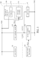
- FIG. 1 is a block diagram illustrating a voltage regulator according to an embodiment of the present invention.
- the voltage regulator 100 employs a hybrid LDO regulator design, and thus includes a first regulator circuit 102 and a second regulator circuit 104.
- the first regulator circuit 102 is coupled between a first power rail VDD and an output node N_OUT of the voltage regulator 100.
- the second regulator circuit 104 is coupled between a second power rail GND and the output node N_OUT of the voltage regulator 100.
- the first power rail VDD is used to deliver a supply voltage
- the second power rail GND is used to deliver a ground voltage.
- the voltage regulator 100 is used for providing a load device 10 with a regulated voltage V_OUT that is generated at the output node N_OUT.
- the first regulator circuit 102 is a part of a series regulator such that the load device 10 and the first regulator circuit 102 are connected in series
- the second regulator circuit 104 is a part of a shunt regulator such that the load device 10 and the second regulator circuit 104 are connected in parallel.
- the voltage regulator 100 further includes a first control loop circuit 106 and a second control loop circuit 108.
- a combination of the first regulator circuit 102 and the first control loop circuit 106 acts as one series regulator, where the first bias voltage VB_1 of the first regulator circuit 102 is adaptively adjusted by the first control loop circuit 106 in response to a load condition at the output node N_OUT of the voltage regulator 100.
- a combination of the second regulator circuit 104 and the second control loop circuit 108 acts as one shunt regulator, where the second bias voltage VB_2 of the second regulator circuit 104 is adaptively adjusted by the second control loop circuit 108 in response to the load condition at the output node N_OUT of the voltage regulator 100.
- the first control loop circuit 106 includes a feedback amplifier 110 and a capacitor 112.
- the feedback amplifier 110 is arranged to generate the first bias voltage VB_1 at its output node N1.
- the capacitor 112 may be implemented by a single capacitor or a combination of discrete small-sized capacitors. That is, the present invention has no limitations on the actual implementation of the capacitor 112. As shown in FIG. 1 , the capacitor 112 is coupled between the first power rail VDD and the output node N1 of the feedback amplifier 110.
- a capacitance value of the capacitor 112 is properly set to thereby achieve the desired bandwidth suppression for the first control loop circuit 106.
- a bandwidth of the first control loop circuit 106 is different from a bandwidth of the second control loop circuit 108.
- the capacitor 112 with a large capacitance value is intentionally introduced to ensure that the bandwidth of the first control loop circuit 106 is much lower than the bandwidth of the second control loop circuit 108.
- the first control loop circuit 106 tracks the load variation at the output node N_OUT and adjusts the first bias voltage VB_1 at a slower speed. Due to the large discrepancy between the bandwidth of the first control loop circuit 106 and the bandwidth of the second control loop circuit 108, the first bias voltage VB_1 adjusted under the bandwidth of the first control loop circuit 106 can be regarded as a constant voltage under the bandwidth of the second control loop circuit 108. In this way, the first regulator circuit 102 may be regarded as a current source for the second regulator circuit 104 under the bandwidth of the second control loop circuit 108.
- the first regulator circuit 102 Since the first regulator circuit 102 is coupled to the first power rail VDD, the first regulator circuit 102 is arranged to perform a voltage-mode voltage regulation operation upon the regulated voltage V_OUT according to the first bias voltage VB_1. Since the second regulator circuit 104 is loaded with a current source (e.g., first regulator circuit 102), the second regulator circuit 104 is arranged to perform a current-mode voltage regulation operation upon the regulated voltage V_OUT according to the second bias voltage VB_2. Further details of the proposed hybrid voltage regulator using a series regulator with bandwidth suppression are described as below.
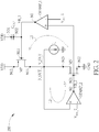
- FIG. 2 is a circuit diagram illustrating a first power-efficient voltage regulator with high reverse leakage rejection according to an embodiment of the present invention.
- the voltage regulator 200 is based on the architecture of the voltage regulator 100 shown in FIG. 1 . That is, the voltage regulator 100 may be implemented using the voltage regulator 200.
- the first regulator circuit 102 may be implemented by a P-channel metal oxide semiconductor (PMOS) transistor MP
- the second regulator circuit 104 may be implemented by an N-channel metal oxide semiconductor (NMOS) transistor MN
- the second control loop circuit 108 may be implemented by an operational amplifier OPAMP_2
- the feedback amplifier 110 of the first control loop circuit 106 may be implemented by an operational amplifier OPAMP_1
- the capacitor 112 of the first control loop circuit 106 may be implemented by a capacitor C CMP .
- a control terminal (i.e., gate) N11 is coupled to an output node N1 of the operational amplifier OPAMP_1
- a first connection terminal (i.e., source) N12 is coupled to the first power rail VDD (which provides a supply voltage)
- a second connection terminal (i.e., drain) N13 is coupled to the output node N_OUT of the voltage regulator 200.
- a control terminal (i.e., gate) N21 is coupled to an input node of the operational amplifier OPAMP_1 and an output node N2 of the operational amplifier OPAMP_2, a first connection terminal (i.e., source) N22 is coupled to the second power rail GND (which provides a ground voltage), and a second connection terminal (i.e., drain) N23 is coupled to the output node N_OUT of the voltage regulator 200.
- the operational amplifier OPAMP_2 is a differential input, single-ended output amplifier having a non-inverting input node (+) arranged to receive the regulated voltage V_OUT generated at the output node N_OUT of the voltage regulator 200 and an inverting input node (-) arranged to receive a reference voltage V REF _2, where an output voltage generated at the output node N2 acts as the second bias voltage VB_2 supplied to the control terminal N21 of the NMOS transistor MN.
- the operational amplifier OPAMP_1 is a differential input, single-ended output amplifier having a non-inverting input node (+) arranged to receive the output voltage generated from the operational amplifier OPAMP_1 and an inverting input node (-) arranged to receive a reference voltage V REF _1, where an output voltage generated at the output node N1 acts as the first bias voltage VB_1 supplied to the control terminal N11 of the PMOS transistor MP.
- a first end N31 and a second end N32 of the capacitor C CMP are coupled to the first power rail VDD and the control terminal N11 of the PMOS transistor MP, respectively.
- a capacitance value of the capacitor C CMP is properly set to ensure that a bandwidth of a first control loop L1 (which is realized by capacitor C CMP and operational amplifier OPAMP_1) is much lower than a bandwidth of a second control loop L2 (which is realized by operational amplifier OPAMP_2).
- the bandwidth of the first control loop L1 is in an order of Kilo Hertz (KHz)
- the bandwidth of the second control loop L2 is in an order of Mega Hertz (MHz).
- the first bias voltage VB_1 slowly adjusted under the low bandwidth of the first control loop L1 is regarded as a constant voltage under the high bandwidth of the second control loop L2, such that the PMOS transistor MP is regarded as a current source for the NMOS transistor MN under the high bandwidth of the second control loop L2. Since the NMOS transistor MN is loaded with a current source, a current-mode voltage regulator is achieved and has strong reverse power supply rejection ratio (PSRR) to block the leakage current introduced by the load device 10 from affecting other load device 20 powered by the first power rail VDD.
- PSRR reverse power supply rejection ratio
- the load device 10 may be a digital intensive circuit such as a time to digital converter (TDC) which operates according to a reference clock, and the load device 20 may be a supply-sensitive circuit.
- TDC time to digital converter
- a time-variant load current I L is drawn from the output node N_OUT by the load device 10 due to the fact that the load device 10 includes clock-based processing circuit(s). Since the PMOS transistor MP (which is controlled by a low-bandwidth loop) acts as a current source for the NMOS transistor MN (which is controlled by a high-bandwidth loop), the required reverse leakage isolation is provided by the PMOS transistor MP.
- TDC time to digital converter
- the first end N31 of the capacitor C CMP is directly connected to the first power rail VDD (which is directly connected to the first connection terminal N12 of the PMOS transistor MP), and the second end N32 of the capacitor C CMP is directly connected to the control terminal N11 of the PMOS transistor MP.
- the capacitor C CMP acts as an alternating current (AC) shorted circuit from the source to the gate of the PMOS transistor MP that is a part of the series regulator.
- AC alternating current
- the operational amplifier OPAMP_1 can be configured to have a gain larger than a unity gain. In this way, the PSRR performance can be further improved. To put it another way, the in-band PSRR can be improved due to gain contribution from the control loop.
- the control loop L1 is absent, and a fixed bias voltage is applied to the control terminal N11 of the PMOS transistor MP for enforcing the PMOS transistor MP to provide a large constant current not smaller than a maximum load current I L that may be drawn from the load device 10.
- the PMOS transistor MP consumes large power to cover the load variation under process corner and temperature.
- the present invention proposes using the control loop L1 to adaptively track the output load (e.g., load current I L ) and adjust the first bias voltage VB_1. Since the first bias voltage VB_1 is adaptively adjusted in response to a load condition, the power consumption of the PMOS transistor MP can be reduced. In this way, the power efficiency of the voltage regulator with high reverse leakage rejection/isolation can be improved. To put it simply, the proposed voltage regulator 200 is a power-efficient LDO regulator with high reverse PSRR.
- the reference voltage V REF _1 provided to the operational amplifier OPAMP_1 can also control the transconductance (g m ) parameter of the NMOS transistor MN that is a part of the shunt regulator.
- the bandwidth of the control loop L2 can be tuned by the setting of the reference voltage V REF _1.
- this is for illustrative purposes only, and is not meant to be a limitation of the present invention.
- the operational amplifier OPAMP_1 is a differential input, single-ended output amplifier.
- FIG. 3 is a circuit diagram illustrating a first differential input, single-ended output amplifier according to an embodiment of the present invention.
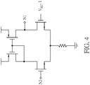
- FIG. 4 is a circuit diagram illustrating a second differential input, single-ended output amplifier according to an embodiment of the present invention.
- the operational amplifier OPAMP_1 shown in FIG. 2 may be implemented by one of the differential input, single-ended output amplifiers 300 and 400, depending upon the actual design considerations.
- FIG. 5 is a circuit diagram illustrating a second power-efficient voltage regulator with high reverse leakage rejection according to an embodiment of the present invention.
- the voltage regulator 500 is also based on the architecture of the voltage regulator 100 shown in FIG. 1 . That is, the voltage regulator 100 may be implemented using the voltage regulator 500.
- the first regulator circuit 102 may be implemented by a PMOS transistor MP
- the second regulator circuit 104 may be implemented by an NMOS transistor MN
- the second control loop circuit 108 may be implemented by an operational amplifier OPAMP_2
- the feedback amplifier 110 of the first control loop circuit 106 may be implemented by an operational amplifier OPAMP_3
- the capacitor 112 of the first control loop circuit 106 may be implemented by a capacitor C CMP .
- the operational amplifier OPAMP_3 is a single-ended input, single-ended output amplifier. Hence, the operational amplifier OPAMP_3 generates the first bias voltage VB_1 at its output node N3 according to the voltage output at the output node N2 of the operational amplifier OPAMP_2, where the voltage output at the output node N2 of the operational amplifier OPAMP_2 also serves as the second bias voltage VB_2.
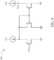
- FIG. 6 is a circuit diagram illustrating a first single-ended input, single-ended output amplifier according to an embodiment of the present invention.
- FIG. 7 is a circuit diagram illustrating a second single-ended input, single-ended output amplifier according to an embodiment of the present invention.
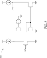
- FIG. 8 is a circuit diagram illustrating a third single-ended input, single-ended output amplifier according to an embodiment of the present invention.
- the operational amplifier OPAMP_3 shown in FIG. 5 may be implemented by one of the single-ended input, single-ended output amplifiers 600, 700, and 800, depending upon the actual design considerations.
- the present invention may also be defined by means of the following numbered clauses.
Landscapes
- Engineering & Computer Science (AREA)
- Physics & Mathematics (AREA)
- Electromagnetism (AREA)
- General Physics & Mathematics (AREA)
- Radar, Positioning & Navigation (AREA)
- Automation & Control Theory (AREA)
- Power Engineering (AREA)
- Continuous-Control Power Sources That Use Transistors (AREA)
Abstract
Description
- This application claims the benefit of
U.S. provisional application No. 62/756,613 - The present invention relates to providing a regulated voltage, and more particularly, to a hybrid voltage regulator using a bandwidth suppressed series regulator and an associated voltage regulating method.
- A voltage regulator is used to generate a regulated voltage that is essential for electronic circuitry. For example, the voltage regulator may be implemented by a low dropout (LDO) regulator that is a linear regulator capable of maintaining a constant voltage output through a feedback loop. Linear regulators exist in two basic forms, series regulators and shunt regulators. With regard to a series regulator, it is placed between a voltage source and a load device. With regard to a shunt regulator, it is placed in parallel with a load device. Each of the series regulator and the shunt regulator has advantages and disadvantages. There is a need for an innovative hybrid voltage regulator which can have good power efficiency and high reverse leakage rejection/isolation.
- One of the objectives of the claimed invention is to provide a hybrid voltage regulator using a bandwidth suppressed series regulator and an associated voltage regulating method.
- According to a first aspect, an exemplary voltage regulator for providing a load device with a regulated voltage is disclosed. The exemplary voltage regulator includes a first regulator circuit, a second regulator circuit, a first control loop circuit, and a second control loop circuit. The first regulator circuit is coupled between a first power rail and an output node of the voltage regulator, wherein the regulated voltage is generated at the output node of the voltage regulator, and the load device and the first regulator circuit are connected in series. The second regulator circuit is coupled between a second power rail and the output node of the voltage regulator, wherein the load device and the second regulator circuit are connected in parallel. The first control loop circuit is arranged to adaptively adjust a first bias voltage of the first regulator circuit in response to a load condition at the output node of the voltage regulator. The first control loop circuit comprises a feedback amplifier and a capacitor. The feedback amplifier is arranged to generate the first bias voltage at an output node of the feedback amplifier. The capacitor is coupled between the first power rail and the output node of the feedback amplifier. The second control loop circuit is arranged to adaptively adjust a second bias voltage of the second regulator circuit in response to the load condition at the output node of the voltage regulator.
- According to a second aspect of the present invention, an exemplary voltage regulating method for providing a load device with a regulated voltage is disclosed. The exemplary voltage regulating method comprises: performing a voltage-mode voltage regulation operation upon the regulated voltage according to a first bias voltage, wherein the regulated voltage is generated at an output node that is coupled to the load device; performing a current-mode voltage regulation operation upon the regulated voltage according to a second bias voltage; adaptively adjusting the first bias voltage of the voltage-mode voltage regulation operation in response to a load condition at the output node, comprising generating, by a feedback amplifier, the first bias voltage at an output node of the feedback amplifier, wherein a capacitor is coupled between a power rail and the output node of the feedback amplifier; and adaptively adjusting the second bias voltage of the current-mode voltage regulation operation in response to the load condition at the output node.
- These and other objectives of the present invention will no doubt become obvious to those of ordinary skill in the art after reading the following detailed description of the preferred embodiment that is illustrated in the various figures and drawings.
-
-
FIG. 1 is a block diagram illustrating a voltage regulator according to an embodiment of the present invention. -
FIG. 2 is a circuit diagram illustrating a first power-efficient voltage regulator with high reverse leakage rejection according to an embodiment of the present invention. -
FIG. 3 is a circuit diagram illustrating a first differential input, single-ended output amplifier according to an embodiment of the present invention. -
FIG. 4 is a circuit diagram illustrating a second differential input, single-ended output amplifier according to an embodiment of the present invention. -
FIG. 5 is a circuit diagram illustrating a second power-efficient voltage regulator with high reverse leakage rejection according to an embodiment of the present invention. -
FIG. 6 is a circuit diagram illustrating a first single-ended input, single-ended output amplifier according to an embodiment of the present invention. -
FIG. 7 is a circuit diagram illustrating a second single-ended input, single-ended output amplifier according to an embodiment of the present invention. -
FIG. 8 is a circuit diagram illustrating a third single-ended input, single-ended output amplifier according to an embodiment of the present invention. - Certain terms are used throughout the following description and claims, which refer to particular components. As one skilled in the art will appreciate, electronic equipment manufacturers may refer to a component by different names. This document does not intend to distinguish between components that differ in name but not in function. In the following description and in the claims, the terms "include" and "comprise" are used in an open-ended fashion, and thus should be interpreted to mean "include, but not limited to ...". Also, the term "couple" is intended to mean either an indirect or direct electrical connection. Accordingly, if one device is coupled to another device, that connection may be through a direct electrical connection, or through an indirect electrical connection via other devices and connections.
-
FIG. 1 is a block diagram illustrating a voltage regulator according to an embodiment of the present invention. Thevoltage regulator 100 employs a hybrid LDO regulator design, and thus includes afirst regulator circuit 102 and asecond regulator circuit 104. Thefirst regulator circuit 102 is coupled between a first power rail VDD and an output node N_OUT of thevoltage regulator 100. Thesecond regulator circuit 104 is coupled between a second power rail GND and the output node N_OUT of thevoltage regulator 100. In this embodiment, the first power rail VDD is used to deliver a supply voltage, and the second power rail GND is used to deliver a ground voltage. Thevoltage regulator 100 is used for providing aload device 10 with a regulated voltage V_OUT that is generated at the output node N_OUT. In accordance with the hybrid LDO regulator design, thefirst regulator circuit 102 is a part of a series regulator such that theload device 10 and thefirst regulator circuit 102 are connected in series, and thesecond regulator circuit 104 is a part of a shunt regulator such that theload device 10 and thesecond regulator circuit 104 are connected in parallel. - The
voltage regulator 100 further includes a firstcontrol loop circuit 106 and a secondcontrol loop circuit 108. A combination of thefirst regulator circuit 102 and the firstcontrol loop circuit 106 acts as one series regulator, where the first bias voltage VB_1 of thefirst regulator circuit 102 is adaptively adjusted by the firstcontrol loop circuit 106 in response to a load condition at the output node N_OUT of thevoltage regulator 100. A combination of thesecond regulator circuit 104 and the secondcontrol loop circuit 108 acts as one shunt regulator, where the second bias voltage VB_2 of thesecond regulator circuit 104 is adaptively adjusted by the secondcontrol loop circuit 108 in response to the load condition at the output node N_OUT of thevoltage regulator 100. - In this embodiment, the first
control loop circuit 106 includes a feedback amplifier 110 and acapacitor 112. The feedback amplifier 110 is arranged to generate the first bias voltage VB_1 at its output node N1. Thecapacitor 112 may be implemented by a single capacitor or a combination of discrete small-sized capacitors. That is, the present invention has no limitations on the actual implementation of thecapacitor 112. As shown inFIG. 1 , thecapacitor 112 is coupled between the first power rail VDD and the output node N1 of the feedback amplifier 110. - A capacitance value of the
capacitor 112 is properly set to thereby achieve the desired bandwidth suppression for the firstcontrol loop circuit 106. With a proper setting of the capacitance value of thecapacitor 112, a bandwidth of the firstcontrol loop circuit 106 is different from a bandwidth of the secondcontrol loop circuit 108. For example, thecapacitor 112 with a large capacitance value is intentionally introduced to ensure that the bandwidth of the firstcontrol loop circuit 106 is much lower than the bandwidth of the secondcontrol loop circuit 108. Compared to the secondcontrol loop circuit 108 which tracks the load variation at the output node N_OUT and adjusts the second bias voltage VB_2 at a faster speed, the firstcontrol loop circuit 106 tracks the load variation at the output node N_OUT and adjusts the first bias voltage VB_1 at a slower speed. Due to the large discrepancy between the bandwidth of the firstcontrol loop circuit 106 and the bandwidth of the secondcontrol loop circuit 108, the first bias voltage VB_1 adjusted under the bandwidth of the firstcontrol loop circuit 106 can be regarded as a constant voltage under the bandwidth of the secondcontrol loop circuit 108. In this way, thefirst regulator circuit 102 may be regarded as a current source for thesecond regulator circuit 104 under the bandwidth of the secondcontrol loop circuit 108. Since thefirst regulator circuit 102 is coupled to the first power rail VDD, thefirst regulator circuit 102 is arranged to perform a voltage-mode voltage regulation operation upon the regulated voltage V_OUT according to the first bias voltage VB_1. Since thesecond regulator circuit 104 is loaded with a current source (e.g., first regulator circuit 102), thesecond regulator circuit 104 is arranged to perform a current-mode voltage regulation operation upon the regulated voltage V_OUT according to the second bias voltage VB_2. Further details of the proposed hybrid voltage regulator using a series regulator with bandwidth suppression are described as below. -
FIG. 2 is a circuit diagram illustrating a first power-efficient voltage regulator with high reverse leakage rejection according to an embodiment of the present invention. Thevoltage regulator 200 is based on the architecture of thevoltage regulator 100 shown inFIG. 1 . That is, thevoltage regulator 100 may be implemented using thevoltage regulator 200. For example, thefirst regulator circuit 102 may be implemented by a P-channel metal oxide semiconductor (PMOS) transistor MP, thesecond regulator circuit 104 may be implemented by an N-channel metal oxide semiconductor (NMOS) transistor MN, the secondcontrol loop circuit 108 may be implemented by an operational amplifier OPAMP_2, the feedback amplifier 110 of the firstcontrol loop circuit 106 may be implemented by an operational amplifier OPAMP_1, and thecapacitor 112 of the firstcontrol loop circuit 106 may be implemented by a capacitor CCMP. - Regarding the PMOS transistor MP, a control terminal (i.e., gate) N11 is coupled to an output node N1 of the operational amplifier OPAMP_1, a first connection terminal (i.e., source) N12 is coupled to the first power rail VDD (which provides a supply voltage), and a second connection terminal (i.e., drain) N13 is coupled to the output node N_OUT of the
voltage regulator 200. - Regarding the NMOS transistor MN, a control terminal (i.e., gate) N21 is coupled to an input node of the operational amplifier OPAMP_1 and an output node N2 of the operational amplifier OPAMP_2, a first connection terminal (i.e., source) N22 is coupled to the second power rail GND (which provides a ground voltage), and a second connection terminal (i.e., drain) N23 is coupled to the output node N_OUT of the
voltage regulator 200. - The operational amplifier OPAMP_2 is a differential input, single-ended output amplifier having a non-inverting input node (+) arranged to receive the regulated voltage V_OUT generated at the output node N_OUT of the
voltage regulator 200 and an inverting input node (-) arranged to receive a reference voltage VREF_2, where an output voltage generated at the output node N2 acts as the second bias voltage VB_2 supplied to the control terminal N21 of the NMOS transistor MN. In this example, the operational amplifier OPAMP_1 is a differential input, single-ended output amplifier having a non-inverting input node (+) arranged to receive the output voltage generated from the operational amplifier OPAMP_1 and an inverting input node (-) arranged to receive a reference voltage VREF_1, where an output voltage generated at the output node N1 acts as the first bias voltage VB_1 supplied to the control terminal N11 of the PMOS transistor MP. - A first end N31 and a second end N32 of the capacitor CCMP are coupled to the first power rail VDD and the control terminal N11 of the PMOS transistor MP, respectively. A capacitance value of the capacitor CCMP is properly set to ensure that a bandwidth of a first control loop L1 (which is realized by capacitor CCMP and operational amplifier OPAMP_1) is much lower than a bandwidth of a second control loop L2 (which is realized by operational amplifier OPAMP_2). By way of example, but not limitation, the bandwidth of the first control loop L1 is in an order of Kilo Hertz (KHz), and the bandwidth of the second control loop L2 is in an order of Mega Hertz (MHz). Due to the large discrepancy between the low bandwidth of the first control loop L1 and the high bandwidth of the second control loop L2, the first bias voltage VB_1 slowly adjusted under the low bandwidth of the first control loop L1 is regarded as a constant voltage under the high bandwidth of the second control loop L2, such that the PMOS transistor MP is regarded as a current source for the NMOS transistor MN under the high bandwidth of the second control loop L2. Since the NMOS transistor MN is loaded with a current source, a current-mode voltage regulator is achieved and has strong reverse power supply rejection ratio (PSRR) to block the leakage current introduced by the
load device 10 from affectingother load device 20 powered by the first power rail VDD. For example, theload device 10 may be a digital intensive circuit such as a time to digital converter (TDC) which operates according to a reference clock, and theload device 20 may be a supply-sensitive circuit. A time-variant load current IL is drawn from the output node N_OUT by theload device 10 due to the fact that theload device 10 includes clock-based processing circuit(s). Since the PMOS transistor MP (which is controlled by a low-bandwidth loop) acts as a current source for the NMOS transistor MN (which is controlled by a high-bandwidth loop), the required reverse leakage isolation is provided by the PMOS transistor MP. - In this embodiment, the first end N31 of the capacitor CCMP is directly connected to the first power rail VDD (which is directly connected to the first connection terminal N12 of the PMOS transistor MP), and the second end N32 of the capacitor CCMP is directly connected to the control terminal N11 of the PMOS transistor MP. Hence, the capacitor CCMP acts as an alternating current (AC) shorted circuit from the source to the gate of the PMOS transistor MP that is a part of the series regulator. This would improve the PSRR performance. Furthermore, the operational amplifier OPAMP_1 can be configured to have a gain larger than a unity gain. In this way, the PSRR performance can be further improved. To put it another way, the in-band PSRR can be improved due to gain contribution from the control loop.
- In a typical shunt regulator design, the control loop L1 is absent, and a fixed bias voltage is applied to the control terminal N11 of the PMOS transistor MP for enforcing the PMOS transistor MP to provide a large constant current not smaller than a maximum load current IL that may be drawn from the
load device 10. Hence, the PMOS transistor MP consumes large power to cover the load variation under process corner and temperature. The present invention proposes using the control loop L1 to adaptively track the output load (e.g., load current IL) and adjust the first bias voltage VB_1. Since the first bias voltage VB_1 is adaptively adjusted in response to a load condition, the power consumption of the PMOS transistor MP can be reduced. In this way, the power efficiency of the voltage regulator with high reverse leakage rejection/isolation can be improved. To put it simply, the proposedvoltage regulator 200 is a power-efficient LDO regulator with high reverse PSRR. - It should be noted that the reference voltage VREF_1provided to the operational amplifier OPAMP_1 can also control the transconductance (gm) parameter of the NMOS transistor MN that is a part of the shunt regulator. Hence, the bandwidth of the control loop L2 can be tuned by the setting of the reference voltage VREF_1. However, this is for illustrative purposes only, and is not meant to be a limitation of the present invention.
- As shown in
FIG. 2 , the operational amplifier OPAMP_1 is a differential input, single-ended output amplifier.FIG. 3 is a circuit diagram illustrating a first differential input, single-ended output amplifier according to an embodiment of the present invention.FIG. 4 is a circuit diagram illustrating a second differential input, single-ended output amplifier according to an embodiment of the present invention. The operational amplifier OPAMP_1 shown inFIG. 2 may be implemented by one of the differential input, single-endedoutput amplifiers 300 and 400, depending upon the actual design considerations. -
FIG. 5 is a circuit diagram illustrating a second power-efficient voltage regulator with high reverse leakage rejection according to an embodiment of the present invention. Like thevoltage regulator 200 shown inFIG. 2 , thevoltage regulator 500 is also based on the architecture of thevoltage regulator 100 shown inFIG. 1 . That is, thevoltage regulator 100 may be implemented using thevoltage regulator 500. For example, thefirst regulator circuit 102 may be implemented by a PMOS transistor MP, thesecond regulator circuit 104 may be implemented by an NMOS transistor MN, the secondcontrol loop circuit 108 may be implemented by an operational amplifier OPAMP_2, the feedback amplifier 110 of the firstcontrol loop circuit 106 may be implemented by an operational amplifier OPAMP_3, and thecapacitor 112 of the firstcontrol loop circuit 106 may be implemented by a capacitor CCMP. The major difference between thevoltage regulators -
FIG. 6 is a circuit diagram illustrating a first single-ended input, single-ended output amplifier according to an embodiment of the present invention.FIG. 7 is a circuit diagram illustrating a second single-ended input, single-ended output amplifier according to an embodiment of the present invention.FIG. 8 is a circuit diagram illustrating a third single-ended input, single-ended output amplifier according to an embodiment of the present invention. The operational amplifier OPAMP_3 shown inFIG. 5 may be implemented by one of the single-ended input, single-endedoutput amplifiers - Since a person skilled in the pertinent art can readily understand the operation and function of the
voltage regulator 500 after reading above paragraphs directed to thevoltage regulator 200, further description is omitted here for brevity. - Those skilled in the art will readily observe that numerous modifications and alterations of the device and method may be made while retaining the teachings of the invention. Accordingly, the above disclosure should be construed as limited only by the metes and bounds of the appended claims.
- The present invention may also be defined by means of the following numbered clauses.
- 1. A voltage regulator for providing a load device with a regulated voltage, comprising:
- a first regulator circuit, coupled between a first power rail and an output node of the voltage regulator, wherein the regulated voltage is generated at the output node of the voltage regulator, and the load device and the first regulator circuit are connected in series;
- a second regulator circuit, coupled between a second power rail and the output node of the voltage regulator, wherein the load device and the second regulator circuit are connected in parallel;
- a first control loop circuit, arranged to adaptively adjust a first bias voltage of the first regulator circuit in response to a load condition at the output node of the voltage regulator, wherein the first control loop circuit comprises:
- a feedback amplifier, arranged to generate the first bias voltage at an output node of the feedback amplifier; and
- a capacitor, coupled between the first power rail and the output node of the feedback amplifier; and
- a second control loop circuit, arranged to adaptively adjust a second bias voltage of the second regulator circuit in response to the load condition at the output node of the voltage regulator.
- 2. The voltage regulator of
clause 1, wherein the first regulator circuit comprises:- a transistor, having a control terminal, a first connection terminal, and a second connection terminal, wherein the control terminal is arranged to receive the first bias voltage, the first connection terminal is coupled to the first power rail, and the second connection terminal is coupled to the output node of the voltage regulator;
- wherein a first end and a second end of the capacitor are coupled to the first power rail and the control terminal of the transistor, respectively.
- 3. The voltage regulator of clause 2, wherein the first end of the capacitor is directly connected to the first power rail, and the second end of the capacitor is directly connected to the control terminal of the transistor.
- 4. The voltage regulator of
clause 1, wherein the feedback amplifier is a single-ended input, single-ended output amplifier. - 5. The voltage regulator of
clause 1, wherein the feedback amplifier is a differential input, single-ended output amplifier. - 6. The voltage regulator of
clause 1, wherein a bandwidth of the first control loop circuit is different from a bandwidth of the second control loop circuit. - 7. The voltage regulator of clause 6, wherein the bandwidth of the first control loop circuit is lower than the bandwidth of the second control loop circuit.
- 8. The voltage regulator of clause 7, wherein the first regulator circuit comprises:
- a transistor, having a control terminal, a first connection terminal, and a second connection terminal, wherein the control terminal is arranged to receive the first bias voltage, the first connection terminal is coupled to the first power rail, and the second connection terminal is coupled to the output node of the voltage regulator;
- wherein due to discrepancy between the bandwidth of the first control loop circuit and the bandwidth of the second control loop circuit, the first bias voltage adjusted under the bandwidth of the first control loop circuit is regarded as a constant voltage under the bandwidth of the second control loop circuit.
- 9. The voltage regulator of clause 8, wherein the transistor is regarded as a current source for the second regulator circuit under the bandwidth of the second control loop circuit.
- 10. The voltage regulator of
clause 1, wherein the load device is a digital intensive circuit. - 11. A voltage regulating method for providing a load device with a regulated voltage, comprising:
- performing a voltage-mode voltage regulation operation upon the regulated voltage according to a first bias voltage, wherein the regulated voltage is generated at an output node that is coupled to the load device;
- performing a current-mode voltage regulation operation upon the regulated voltage according to a second bias voltage;
- adaptively adjusting the first bias voltage of the voltage-mode voltage regulation operation in response to a load condition at the output node, comprising:
generating, by a feedback amplifier, the first bias voltage at an output node of the feedback amplifier, wherein a capacitor is coupled between a power rail and the output node of the feedback amplifier; and - adaptively adjusting the second bias voltage of the current-mode voltage regulation operation in response to the load condition at the output node.
- 12. The voltage regulating method of clause 11, wherein the voltage-mode voltage regulation operation is performed by a regulator circuit comprising:
- a transistor, having a control terminal, a first connection terminal, and a second connection terminal, wherein the control terminal is arranged to receive the first bias voltage, the first connection terminal is coupled to the power rail, and the second connection terminal is coupled to the output node;
- wherein a first end and a second end of the capacitor are coupled to the first power rail and the control terminal of the transistor, respectively.
- 13. The voltage regulating method of clause 12, wherein the first end of the capacitor is directly connected to the first power rail, and the second end of the capacitor is directly connected to the control terminal of the transistor.
- 14. The voltage regulating method of clause 11, wherein the feedback amplifier is a single-ended input, single-ended output amplifier.
- 15. The voltage regulating method of clause 11, wherein the feedback amplifier is a differential input, single-ended output amplifier.
- 16. The voltage regulating method of clause 11, wherein a first loop bandwidth of adaptively adjusting the first bias voltage of the voltage-mode voltage regulation operation is different from a second loop bandwidth of adaptively adjusting the first second voltage of the current-mode voltage regulation operation.
- 17. The voltage regulating method of clause 16, wherein the first loop bandwidth is lower than the second loop bandwidth.
- 18. The voltage regulating method of clause 17, wherein the voltage-mode voltage regulation operation is performed by a regulator circuit comprising:
- a transistor, having a control terminal, a first connection terminal, and a second connection terminal, wherein the control terminal is arranged to receive the first bias voltage, the first connection terminal is coupled to the power rail, and the second connection terminal is coupled to the output node of the voltage regulator;
- wherein due to discrepancy between the first loop bandwidth and the second loop bandwidth, the first bias voltage adjusted under the first loop bandwidth is regarded as a constant voltage under the second loop bandwidth.
- 19. The voltage regulating method of clause 18, wherein the transistor is regarded as a current source for the current-mode voltage regulation operation under the second loop bandwidth.
- 20. The voltage regulating method of clause 11, wherein the load device is a digital intensive circuit.
Claims (15)
- A voltage regulator (100, 200, 500) for providing a load device (10, 20) with a regulated voltage, comprising:a first regulator circuit (102), coupled between a first power rail and an output node of the voltage regulator (100, 200, 500), wherein the regulated voltage is generated at the output node of the voltage regulator (100, 200, 500), and the load device (10, 20) and the first regulator circuit (102) are connected in series;a second regulator circuit (104), coupled between a second power rail and the output node of the voltage regulator (100, 200, 500), wherein the load device (10, 20) and the second regulator circuit (104) are connected in parallel;a first control loop circuit (106), arranged to adaptively adjust a first bias voltage of the first regulator circuit (102) in response to a load condition at the output node of the voltage regulator (100, 200, 500), wherein the first control loop circuit (106) comprises:a feedback amplifier (110), arranged to generate the first bias voltage at an output node of the feedback amplifier (110); anda capacitor (112), coupled between the first power rail and the output node of the feedback amplifier (110); anda second control loop circuit (108), arranged to adaptively adjust a second bias voltage of the second regulator circuit (104) in response to the load condition at the output node of the voltage regulator (100, 200, 500).
- The voltage regulator (100, 200, 500) of claim 1, wherein the first regulator circuit (102) comprises:a transistor, having a control terminal, a first connection terminal, and a second connection terminal, wherein the control terminal is arranged to receive the first bias voltage, the first connection terminal is coupled to the first power rail, and the second connection terminal is coupled to the output node of the voltage regulator (100, 200, 500);wherein a first end and a second end of the capacitor (112) are coupled to the first power rail and the control terminal of the transistor, respectively.
- The voltage regulator (100, 200, 500) of claim 2, wherein the first end of the capacitor (112) is directly connected to the first power rail, and the second end of the capacitor (112) is directly connected to the control terminal of the transistor.
- The voltage regulator (100, 200, 500) of claim 1, wherein the feedback amplifier (110) is a single-ended input, single-ended output amplifier; or
wherein the feedback amplifier (11) is a differential input, single-ended output amplifier; or
wherein the load device (10, 20) is a digital intensive circuit. - The voltage regulator (100, 200, 500) of claim 1, wherein a bandwidth of the first control loop circuit (108) is different from a bandwidth of the second control loop circuit.
- The voltage regulator (100, 200, 500) of claim 5, wherein the bandwidth of the first control loop circuit (106) is lower than the bandwidth of the second control loop circuit (108).
- The voltage regulator (100, 200, 500) of claim 6, wherein the first regulator circuit (102) comprises:a transistor, having a control terminal, a first connection terminal, and a second connection terminal, wherein the control terminal is arranged to receive the first bias voltage, the first connection terminal is coupled to the first power rail, and the second connection terminal is coupled to the output node of the voltage regulator (100, 200, 500);wherein due to discrepancy between the bandwidth of the first control loop circuit (106) and the bandwidth of the second control loop circuit (108), the first bias voltage adjusted under the bandwidth of the first control loop circuit (106) is regarded as a constant voltage under the bandwidth of the second control loop circuit (108).
- The voltage regulator (100, 200, 500) of claim 7, wherein the transistor is regarded as a current source for the second regulator circuit (102) under the bandwidth of the second control loop circuit (108).
- A voltage regulating method for providing a load device (10, 20) with a regulated voltage, comprising:performing a voltage-mode voltage regulation operation upon the regulated voltage according to a first bias voltage, wherein the regulated voltage is generated at an output node that is coupled to the load device (10, 20);performing a current-mode voltage regulation operation upon the regulated voltage according to a second bias voltage;adaptively adjusting the first bias voltage of the voltage-mode voltage regulation operation in response to a load condition at the output node, comprising:
generating, by a feedback amplifier (110), the first bias voltage at an output node of the feedback amplifier (110), wherein a capacitor (112) is coupled between a power rail and the output node of the feedback amplifier (110); andadaptively adjusting the second bias voltage of the current-mode voltage regulation operation in response to the load condition at the output node. - The voltage regulating method of claim 9, wherein the voltage-mode voltage regulation operation is performed by a regulator circuit comprising:a transistor, having a control terminal, a first connection terminal, and a second connection terminal, wherein the control terminal is arranged to receive the first bias voltage, the first connection terminal is coupled to the power rail, and the second connection terminal is coupled to the output node;wherein a first end and a second end of the capacitor (112) are coupled to the first power rail and the control terminal of the transistor, respectively.
- The voltage regulating method of claim 10, wherein the first end of the capacitor (112) is directly connected to the first power rail, and the second end of the capacitor (112) is directly connected to the control terminal of the transistor.
- The voltage regulating method of claim 9, wherein the feedback amplifier (110) is a single-ended input, single-ended output amplifier; or
wherein the feedback amplifier (110) is a differential input, single-ended output amplifier; or
wherein the load device (10, 20) is a digital intensive circuit. - The voltage regulating method of claim 9, wherein a first loop bandwidth of adaptively adjusting the first bias voltage of the voltage-mode voltage regulation operation is different from a second loop bandwidth of adaptively adjusting the first second voltage of the current-mode voltage regulation operation.
- The voltage regulating method of claim 13, wherein the first loop bandwidth is lower than the second loop bandwidth.
- The voltage regulating method of claim 14, wherein the voltage-mode voltage regulation operation is performed by a regulator circuit comprising:a transistor, having a control terminal, a first connection terminal, and a second connection terminal, wherein the control terminal is arranged to receive the first bias voltage, the first connection terminal is coupled to the power rail, and the second connection terminal is coupled to the output node of the voltage regulator (100, 200, 500);wherein due to discrepancy between the first loop bandwidth and the second loop bandwidth, the first bias voltage adjusted under the first loop bandwidth is regarded as a constant voltage under the second loop bandwidth.
Applications Claiming Priority (2)
| Application Number | Priority Date | Filing Date | Title |
|---|---|---|---|
| US201862756613P | 2018-11-07 | 2018-11-07 | |
| US16/590,391 US11340641B2 (en) | 2018-11-07 | 2019-10-02 | Hybrid voltage regulator using bandwidth suppressed series regulator and associated voltage regulating method |
Publications (1)
| Publication Number | Publication Date |
|---|---|
| EP3650978A1 true EP3650978A1 (en) | 2020-05-13 |
Family
ID=68424688
Family Applications (1)
| Application Number | Title | Priority Date | Filing Date |
|---|---|---|---|
| EP19206322.0A Ceased EP3650978A1 (en) | 2018-11-07 | 2019-10-30 | Hybrid voltage regulator using bandwidth suppressed series regulator and associated voltage regulating method |
Country Status (4)
| Country | Link |
|---|---|
| US (1) | US11340641B2 (en) |
| EP (1) | EP3650978A1 (en) |
| CN (1) | CN111158416B (en) |
| TW (1) | TWI701894B (en) |
Families Citing this family (8)
| Publication number | Priority date | Publication date | Assignee | Title |
|---|---|---|---|---|
| US11658570B2 (en) * | 2020-09-01 | 2023-05-23 | Intel Corporation | Seamless non-linear voltage regulation control to linear control apparatus and method |
| US12164319B2 (en) | 2020-12-19 | 2024-12-10 | Intel Corporation | Dual loop voltage regulator |
| US12506399B2 (en) * | 2021-11-16 | 2025-12-23 | Analog Devices, Inc. | Hybrid linear-boost DC-DC converter with continuous input current regulation |
| KR20230082732A (en) | 2021-12-01 | 2023-06-09 | 삼성전자주식회사 | Low-dropout regulator |
| CN117215358A (en) * | 2022-06-10 | 2023-12-12 | 联发科技股份有限公司 | Low Dropout Voltage Regulator |
| CN115373456B (en) * | 2022-09-20 | 2023-07-07 | 中国电子科技集团公司第二十四研究所 | A Parallel Modulated Low Dropout Linear Regulator with Output Pole Dynamic Tracking Compensation |
| CN115756074B (en) * | 2022-11-10 | 2025-07-11 | 南京邮电大学 | A bias circuit with high and low voltage connection and protection functions |
| US20240291371A1 (en) * | 2023-02-28 | 2024-08-29 | Advanced Micro Devices, Inc. | Multi-frequency voltage converter |
Citations (5)
| Publication number | Priority date | Publication date | Assignee | Title |
|---|---|---|---|---|
| US6441594B1 (en) * | 2001-04-27 | 2002-08-27 | Motorola Inc. | Low power voltage regulator with improved on-chip noise isolation |
| US20080054861A1 (en) * | 2006-09-06 | 2008-03-06 | Vladimir Zlatkovic | Dual path linear voltage regulator |
| US20130307506A1 (en) * | 2012-05-17 | 2013-11-21 | Rf Micro Devices, Inc. | Hybrid regulator with composite feedback |
| US20140266118A1 (en) * | 2013-03-15 | 2014-09-18 | Taiwan Semiconductor Manufacturing Company , Ltd. | Voltage regulator |
| US20150177759A1 (en) * | 2013-12-23 | 2015-06-25 | Ess Technology, Inc. | Voltage Regulator Using Both Shunt and Series Regulation |
Family Cites Families (14)
| Publication number | Priority date | Publication date | Assignee | Title |
|---|---|---|---|---|
| TWI301686B (en) | 2004-08-30 | 2008-10-01 | Monolithic Power Systems Inc | Dc/dc switch mode voltage regulator, method implemented thereon and device for short circuit current ratcheting therein |
| US7221213B2 (en) * | 2005-08-08 | 2007-05-22 | Aimtron Technology Corp. | Voltage regulator with prevention from overvoltage at load transients |
| TWI341074B (en) | 2007-07-06 | 2011-04-21 | Chimei Innolux Corp | Power circuit |
| CN101350557B (en) | 2007-07-18 | 2011-04-27 | 华为技术有限公司 | Apparatus for adjusting power supply |
| US7882482B2 (en) | 2007-10-12 | 2011-02-01 | Monolithic Power Systems, Inc. | Layout schemes and apparatus for high performance DC-DC output stage |
| US8405371B2 (en) | 2008-07-29 | 2013-03-26 | Synopsys, Inc. | Voltage regulator with ripple compensation |
| US9136760B2 (en) | 2012-06-27 | 2015-09-15 | Analog Devices Global | Digital switched mode voltage regulator |
| KR102031199B1 (en) | 2012-12-03 | 2019-10-11 | 한국전자통신연구원 | Voltage regulator having error amplifier of rail-to rail |
| US9298199B2 (en) | 2014-08-13 | 2016-03-29 | Mediatek Inc. | Voltage generating circuit and polar transmitter |
| FR3032309B1 (en) | 2015-02-02 | 2017-06-23 | St Microelectronics Alps Sas | VOLTAGE CONTROL CIRCUIT FOR STRONG AND LOW POWER |
| US9665112B2 (en) * | 2015-05-15 | 2017-05-30 | Analog Devices Global | Circuits and techniques including cascaded LDO regulation |
| US10768647B2 (en) * | 2016-06-23 | 2020-09-08 | Atmel Corporation | Regulators with load-insensitive compensation |
| TWI668562B (en) * | 2017-11-09 | 2019-08-11 | 新唐科技股份有限公司 | System on chip |
| US10775819B2 (en) * | 2019-01-16 | 2020-09-15 | Avago Technologies International Sales Pte. Limited | Multi-loop voltage regulator with load tracking compensation |
-
2019
- 2019-10-02 US US16/590,391 patent/US11340641B2/en active Active
- 2019-10-30 EP EP19206322.0A patent/EP3650978A1/en not_active Ceased
- 2019-11-01 TW TW108139726A patent/TWI701894B/en active
- 2019-11-01 CN CN201911060264.5A patent/CN111158416B/en active Active
Patent Citations (5)
| Publication number | Priority date | Publication date | Assignee | Title |
|---|---|---|---|---|
| US6441594B1 (en) * | 2001-04-27 | 2002-08-27 | Motorola Inc. | Low power voltage regulator with improved on-chip noise isolation |
| US20080054861A1 (en) * | 2006-09-06 | 2008-03-06 | Vladimir Zlatkovic | Dual path linear voltage regulator |
| US20130307506A1 (en) * | 2012-05-17 | 2013-11-21 | Rf Micro Devices, Inc. | Hybrid regulator with composite feedback |
| US20140266118A1 (en) * | 2013-03-15 | 2014-09-18 | Taiwan Semiconductor Manufacturing Company , Ltd. | Voltage regulator |
| US20150177759A1 (en) * | 2013-12-23 | 2015-06-25 | Ess Technology, Inc. | Voltage Regulator Using Both Shunt and Series Regulation |
Also Published As
| Publication number | Publication date |
|---|---|
| US20200142436A1 (en) | 2020-05-07 |
| CN111158416A (en) | 2020-05-15 |
| US11340641B2 (en) | 2022-05-24 |
| TW202019068A (en) | 2020-05-16 |
| TWI701894B (en) | 2020-08-11 |
| CN111158416B (en) | 2022-02-25 |
Similar Documents
| Publication | Publication Date | Title |
|---|---|---|
| US11340641B2 (en) | Hybrid voltage regulator using bandwidth suppressed series regulator and associated voltage regulating method | |
| US8289009B1 (en) | Low dropout (LDO) regulator with ultra-low quiescent current | |
| US7397226B1 (en) | Low noise, low power, fast startup, and low drop-out voltage regulator | |
| US20210223810A1 (en) | Pmos-output ldo with full spectrum psr | |
| EP2031476B1 (en) | Voltage regulator and method for voltage regulation | |
| US11487312B2 (en) | Compensation for low dropout voltage regulator | |
| EP3518070B1 (en) | Voltage regulator apparatus offering low dropout and high power supply rejection | |
| EP1635239A1 (en) | Adaptive biasing concept for current mode voltage regulators | |
| CN101223488A (en) | Standard CMOS Low Noise High PSRR Low Dropout Regulator with New Dynamic Compensation | |
| US11016519B2 (en) | Process compensated gain boosting voltage regulator | |
| KR20060085166A (en) | Compensation technology provides stability over a wide range of output capacitor values | |
| US8669753B2 (en) | Voltage regulator having a phase compensation circuit | |
| CN107526385B (en) | Linear Voltage Regulator | |
| US12487621B2 (en) | Low dropout regulator | |
| US7038431B2 (en) | Zero tracking for low drop output regulators | |
| EP3300235B1 (en) | Voltage regulator | |
| CN115668092B (en) | A transient boost circuit, chip system and device for LDO | |
| Leung et al. | A low-voltage CMOS low-dropout regulator with enhanced loop response | |
| CN111694393A (en) | Low static fast linear regulator | |
| US20180024581A1 (en) | Space and power-saving multiple output regulation circuitry | |
| CN100514246C (en) | Low dropout linear regulator | |
| Yeo et al. | A capacitorless low-dropout regulator with enhanced slew rate and 4.5-μ A quiescent current | |
| EP2789097B1 (en) | Feedforward active decoupling | |
| EP1844381A2 (en) | Standard cmos low-noise high psrr low drop-out regulator with new dynamic compensation | |
| Liu et al. | A High PSR and Fast Transient Response Output-Capacitorless LDO using Gm-Boosting and Capacitive Bulk-Driven Feed-Forward Technique in 22nm CMOS |
Legal Events
| Date | Code | Title | Description |
|---|---|---|---|
| PUAI | Public reference made under article 153(3) epc to a published international application that has entered the european phase |
Free format text: ORIGINAL CODE: 0009012 |
|
| STAA | Information on the status of an ep patent application or granted ep patent |
Free format text: STATUS: THE APPLICATION HAS BEEN PUBLISHED |
|
| AK | Designated contracting states |
Kind code of ref document: A1 Designated state(s): AL AT BE BG CH CY CZ DE DK EE ES FI FR GB GR HR HU IE IS IT LI LT LU LV MC MK MT NL NO PL PT RO RS SE SI SK SM TR |
|
| AX | Request for extension of the european patent |
Extension state: BA ME |
|
| STAA | Information on the status of an ep patent application or granted ep patent |
Free format text: STATUS: REQUEST FOR EXAMINATION WAS MADE |
|
| 17P | Request for examination filed |
Effective date: 20201110 |
|
| RBV | Designated contracting states (corrected) |
Designated state(s): AL AT BE BG CH CY CZ DE DK EE ES FI FR GB GR HR HU IE IS IT LI LT LU LV MC MK MT NL NO PL PT RO RS SE SI SK SM TR |
|
| STAA | Information on the status of an ep patent application or granted ep patent |
Free format text: STATUS: EXAMINATION IS IN PROGRESS |
|
| 17Q | First examination report despatched |
Effective date: 20211004 |
|
| P01 | Opt-out of the competence of the unified patent court (upc) registered |
Effective date: 20230607 |
|
| STAA | Information on the status of an ep patent application or granted ep patent |
Free format text: STATUS: THE APPLICATION HAS BEEN REFUSED |
|
| 18R | Application refused |
Effective date: 20250325 |