EP3650868A2 - Amplifier systems for measuring a wide range of current - Google Patents
Amplifier systems for measuring a wide range of current Download PDFInfo
- Publication number
- EP3650868A2 EP3650868A2 EP19202017.0A EP19202017A EP3650868A2 EP 3650868 A2 EP3650868 A2 EP 3650868A2 EP 19202017 A EP19202017 A EP 19202017A EP 3650868 A2 EP3650868 A2 EP 3650868A2
- Authority
- EP
- European Patent Office
- Prior art keywords
- amplifier
- controllable
- sensing circuit
- capacitor
- control circuit
- Prior art date
- Legal status (The legal status is an assumption and is not a legal conclusion. Google has not performed a legal analysis and makes no representation as to the accuracy of the status listed.)
- Granted
Links
Images





Classifications
-
- G—PHYSICS
- G01—MEASURING; TESTING
- G01R—MEASURING ELECTRIC VARIABLES; MEASURING MAGNETIC VARIABLES
- G01R19/00—Arrangements for measuring currents or voltages or for indicating presence or sign thereof
- G01R19/0092—Measuring current only
-
- H—ELECTRICITY
- H03—ELECTRONIC CIRCUITRY
- H03G—CONTROL OF AMPLIFICATION
- H03G1/00—Details of arrangements for controlling amplification
- H03G1/0005—Circuits characterised by the type of controlling devices operated by a controlling current or voltage signal
- H03G1/0088—Circuits characterised by the type of controlling devices operated by a controlling current or voltage signal using discontinuously variable devices, e.g. switch-operated
- H03G1/0094—Circuits characterised by the type of controlling devices operated by a controlling current or voltage signal using discontinuously variable devices, e.g. switch-operated using switched capacitors
-
- G—PHYSICS
- G01—MEASURING; TESTING
- G01R—MEASURING ELECTRIC VARIABLES; MEASURING MAGNETIC VARIABLES
- G01R1/00—Details of instruments or arrangements of the types included in groups G01R5/00 - G01R13/00 and G01R31/00
- G01R1/30—Structural combination of electric measuring instruments with basic electronic circuits, e.g. with amplifier
-
- G—PHYSICS
- G01—MEASURING; TESTING
- G01R—MEASURING ELECTRIC VARIABLES; MEASURING MAGNETIC VARIABLES
- G01R15/00—Details of measuring arrangements of the types provided for in groups G01R17/00 - G01R29/00, G01R33/00 - G01R33/26 or G01R35/00
- G01R15/002—Switches for altering the measuring range or for multitesters
-
- G—PHYSICS
- G01—MEASURING; TESTING
- G01R—MEASURING ELECTRIC VARIABLES; MEASURING MAGNETIC VARIABLES
- G01R15/00—Details of measuring arrangements of the types provided for in groups G01R17/00 - G01R29/00, G01R33/00 - G01R33/26 or G01R35/00
- G01R15/08—Circuits for altering the measuring range
-
- G—PHYSICS
- G01—MEASURING; TESTING
- G01R—MEASURING ELECTRIC VARIABLES; MEASURING MAGNETIC VARIABLES
- G01R19/00—Arrangements for measuring currents or voltages or for indicating presence or sign thereof
- G01R19/25—Arrangements for measuring currents or voltages or for indicating presence or sign thereof using digital measurement techniques
- G01R19/2506—Arrangements for conditioning or analysing measured signals, e.g. for indicating peak values ; Details concerning sampling, digitizing or waveform capturing
-
- H—ELECTRICITY
- H03—ELECTRONIC CIRCUITRY
- H03F—AMPLIFIERS
- H03F1/00—Details of amplifiers with only discharge tubes, only semiconductor devices or only unspecified devices as amplifying elements
- H03F1/56—Modifications of input or output impedances, not otherwise provided for
-
- H—ELECTRICITY
- H03—ELECTRONIC CIRCUITRY
- H03F—AMPLIFIERS
- H03F3/00—Amplifiers with only discharge tubes or only semiconductor devices as amplifying elements
- H03F3/45—Differential amplifiers
- H03F3/45071—Differential amplifiers with semiconductor devices only
- H03F3/45076—Differential amplifiers with semiconductor devices only characterised by the way of implementation of the active amplifying circuit in the differential amplifier
- H03F3/45475—Differential amplifiers with semiconductor devices only characterised by the way of implementation of the active amplifying circuit in the differential amplifier using IC blocks as the active amplifying circuit
-
- G—PHYSICS
- G01—MEASURING; TESTING
- G01D—MEASURING NOT SPECIALLY ADAPTED FOR A SPECIFIC VARIABLE; ARRANGEMENTS FOR MEASURING TWO OR MORE VARIABLES NOT COVERED IN A SINGLE OTHER SUBCLASS; TARIFF METERING APPARATUS; MEASURING OR TESTING NOT OTHERWISE PROVIDED FOR
- G01D5/00—Mechanical means for transferring the output of a sensing member; Means for converting the output of a sensing member to another variable where the form or nature of the sensing member does not constrain the means for converting; Transducers not specially adapted for a specific variable
- G01D5/12—Mechanical means for transferring the output of a sensing member; Means for converting the output of a sensing member to another variable where the form or nature of the sensing member does not constrain the means for converting; Transducers not specially adapted for a specific variable using electric or magnetic means
- G01D5/14—Mechanical means for transferring the output of a sensing member; Means for converting the output of a sensing member to another variable where the form or nature of the sensing member does not constrain the means for converting; Transducers not specially adapted for a specific variable using electric or magnetic means influencing the magnitude of a current or voltage
-
- H—ELECTRICITY
- H03—ELECTRONIC CIRCUITRY
- H03F—AMPLIFIERS
- H03F2200/00—Indexing scheme relating to amplifiers
- H03F2200/129—Indexing scheme relating to amplifiers there being a feedback over the complete amplifier
-
- H—ELECTRICITY
- H03—ELECTRONIC CIRCUITRY
- H03F—AMPLIFIERS
- H03F2200/00—Indexing scheme relating to amplifiers
- H03F2200/261—Amplifier which being suitable for instrumentation applications
-
- H—ELECTRICITY
- H03—ELECTRONIC CIRCUITRY
- H03F—AMPLIFIERS
- H03F2200/00—Indexing scheme relating to amplifiers
- H03F2200/462—Indexing scheme relating to amplifiers the current being sensed
-
- H—ELECTRICITY
- H03—ELECTRONIC CIRCUITRY
- H03F—AMPLIFIERS
- H03F2203/00—Indexing scheme relating to amplifiers with only discharge tubes or only semiconductor devices as amplifying elements covered by H03F3/00
- H03F2203/45—Indexing scheme relating to differential amplifiers
- H03F2203/45116—Feedback coupled to the input of the differential amplifier
-
- H—ELECTRICITY
- H03—ELECTRONIC CIRCUITRY
- H03F—AMPLIFIERS
- H03F2203/00—Indexing scheme relating to amplifiers with only discharge tubes or only semiconductor devices as amplifying elements covered by H03F3/00
- H03F2203/45—Indexing scheme relating to differential amplifiers
- H03F2203/45138—Two or more differential amplifiers in IC-block form are combined, e.g. measuring amplifiers
-
- H—ELECTRICITY
- H03—ELECTRONIC CIRCUITRY
- H03F—AMPLIFIERS
- H03F2203/00—Indexing scheme relating to amplifiers with only discharge tubes or only semiconductor devices as amplifying elements covered by H03F3/00
- H03F2203/45—Indexing scheme relating to differential amplifiers
- H03F2203/45514—Indexing scheme relating to differential amplifiers the FBC comprising one or more switched capacitors, and being coupled between the LC and the IC
-
- H—ELECTRICITY
- H03—ELECTRONIC CIRCUITRY
- H03F—AMPLIFIERS
- H03F2203/00—Indexing scheme relating to amplifiers with only discharge tubes or only semiconductor devices as amplifying elements covered by H03F3/00
- H03F2203/45—Indexing scheme relating to differential amplifiers
- H03F2203/45522—Indexing scheme relating to differential amplifiers the FBC comprising one or more potentiometers
-
- H—ELECTRICITY
- H03—ELECTRONIC CIRCUITRY
- H03F—AMPLIFIERS
- H03F2203/00—Indexing scheme relating to amplifiers with only discharge tubes or only semiconductor devices as amplifying elements covered by H03F3/00
- H03F2203/45—Indexing scheme relating to differential amplifiers
- H03F2203/45534—Indexing scheme relating to differential amplifiers the FBC comprising multiple switches and being coupled between the LC and the IC
Definitions
- Embodiments of the invention relate to electronic systems, and more particularly, to amplifiers.
- Certain electronic devices employ amplifiers for processing signals. When operating open loop, such amplifiers receive an input signal and generate an output signal having a gain in comparison to the input signal.
- Examples of amplifiers include, but are not limited to, operational amplifiers, transimpedance amplifiers, and transconductance amplifiers.
- Certain amplifiers are implemented in a multi-stage configuration to enhance gain and/or performance thereof.
- an amplifier system for measuring a wide range of current is provided herein.
- an amplifier system includes a controllable sensing circuit, a first amplifier including an output configured to drive a device under test (DUT) through the controllable sensing circuit, and a second amplifier including an input coupled to the controllable sensing circuit and operable to generate a measurement signal indicating an amount of measured current of the DUT.
- the amplifier system further includes a control circuit operable to control a configuration or mode of the controllable sensing circuit suitable for a particular type of DUT. Implementing the amplifier system in this manner allows measurement of a wide range of current from a variety of DUTs.
- the amplifier system can operate as a reconfigurable analog front-end (AFE) suitable for measuring a range of current spanning multiple decades for DUTs having various impedances.
- the controllable sensing circuit can include resistors, capacitors, and/or other selectable and/or controllable components to thereby provide configurability for different types of loads, such as DUTs of a range of different impedance values.
- an amplifier system with controllable current measurement characteristics includes a load terminal configured to output a current to a DUT, a controllable sensing circuit, a first amplifier including an output electrically connected to the load terminal through the controllable sensing circuit, a second amplifier including an input coupled to the controllable sensing circuit, and a control circuit operable to control an impedance of the controllable sensing circuit.
- the second amplifier is operable to generate a measurement signal indicating a detected amount of the current outputted from the load terminal.
- an electronic module with controllable current measurement characteristics includes a module substrate, and an amplifier die attached to the module substrate.
- the amplifier die includes a load pin configured to output a current, a first amplifier, a controllable sensing circuit electrically connected between an output of the first amplifier and the load pin, a second amplifier including a first input electrically connected to the output of the first amplifier and a second input electrically connected to the load pin, the second amplifier operable to generate a measurement signal indicating a detected amount of the current outputted from the load pin, and a control circuit operable to control an impedance of the controllable sensing circuit.
- a method of controllable current measurement in an amplifier system includes controlling an impedance of a controllable sensing circuit using a control circuit, providing a current from an output terminal to a DUT, driving the output terminal through the controllable sensing circuit using a first amplifier, generating a voltage across the controllable sensing circuit in response to the current, and generating a measurement signal based on amplifying the voltage across the controllable sensing circuit using a second amplifier so as to measure the current.
- an amplifier system with controllable current measurement characteristics includes a first load terminal and a second load terminal, an amplifier including an inverting input electrically connected to the first load terminal and a non-inverting input electrically connected to the second load terminal, a first controllable sensing circuit electrically connected between a non-inverting output of the amplifier and the inverting input of the amplifier, a second controllable sensing circuit electrically connected between an inverting output of the amplifier and the non-inverting input of the amplifier, and a control circuit operable to control an impedance of the first controllable sensing circuit and an impedance of the second controllable sensing circuit.
- an amplifier system includes a controllable sensing circuit, a first amplifier including an output configured to drive a device under test (DUT) through the controllable sensing circuit, and a second amplifier including an input coupled to the controllable sensing circuit and operable to generate a measurement signal indicating an amount of current flowing to the DUT.
- the amplifier system further includes a control circuit operable to control a configuration or mode of the controllable sensing circuit suitable for measuring the current of a particular type of DUT.
- the amplifier system can operate as a reconfigurable analog front-end (AFE) suitable for measuring a range of current spanning multiple decades for DUTs having various impedances.
- AFE reconfigurable analog front-end
- the controllable sensing circuit can include resistors, capacitors, and/or other selectable and/or controllable components to thereby provide configurability for different types of loads, such as DUTs of a range of different impedance values.
- controllable sensing circuit is connectable between the output of the first amplifier and an inverting input to the first amplifier, thereby controlling an amount of feedback provided to the first amplifier. For instance, an amount of resistive and/or capacitive feedback to the first amplifier can be controlled to achieve desired operating characteristics for a particular DUT and/or application.
- the amplifier systems herein can be incorporated on a semiconductor chip suitable for measuring current from DUTs of a range of different impedances.
- the first amplifier is implemented as an operational amplifier, such as a multi-stage operational amplifier that drives the DUT through the controllable sensing circuit.
- the second amplifier is implemented as an instrumentation amplifier, thereby relaxing constraints on input impedance matching and/or providing enhanced measurement accuracy.
- the amplifier systems herein operate stably when connected with negative feedback.
- the controllable sensing circuit can also be configured to provide feedback and/or compensation to maintain stability.
- an amplifier system without such configurability can exhibit oscillation and/or other unstable behavior under certain load conditions.
- the amplifier system can be implemented with switches for selectively providing local feedback to the first amplifier.
- the amplifier system is coupled to an interface or bus, such as an inter-Integrated Circuit (I 2 C) bus, a General Purpose Input Output (GPIO) bus, and/or other suitable interface.
- I 2 C inter-Integrated Circuit
- GPIO General Purpose Input Output
- the amplifier system's control circuit receives digital data from the bus used to control a configuration or setting of the amplifier system.
- the amplifier system can be fabricated on a semiconductor die or chip, and a user can digitally program a desired configuration or mode of the controllable sensing circuit using the bus. Implementing the amplifier system in this manner provides a convenient and flexible mechanism for user configurability.
- the amplifier systems herein can be used in a wide range of applications, including, but not limited to, current measurement of sensors.
- an amplifier system can be used to measure a sensor's current, thereby detecting various changes in environmental quantities or conditions.
- the amplifier system also biases the sensor and/or measures a sensor's bias voltage to aid in enhancing measurement accuracy and/or to protect the sensor from damage from overvoltage or other improper biasing.
- a processing system for controlling an input to the first amplifier.
- the processing system can control a bias voltage of the DUT by setting a signal level to the non-inverting input of the first amplifier.
- the processing system processes the measurement signal from the second amplifier and/or other measurement signals to control the input signal level to the first amplifier. Accordingly, the processing system can operate in a feedback loop.
- the processing system can be implemented in a wide variety of ways.
- the processing system includes an analog-to-digital converter (ADC) for generating digital input data based on the measurement signal, a digital processing circuit for processing the digital input data to generate digital output data, and a digital-to-analog converter (DAC) for controlling the input signal to the first amplifier based on the digital output data.
- ADC analog-to-digital converter
- DAC digital-to-analog converter
- the digital processing circuit can provide digital integration, digital gain, and/or other desired digital processing to provide a type of feedback desirable for a particular configuration of the amplifier system chosen for a given application and/or type of DUT.
- a processing chip such as a field-programmable gate array (FPGA) and/or microprocessor, is commonly packaged with an amplifier chip in a multi-chip module.
- the amplifier chip can include the configurable amplifier system thereon and generate at least one feedback signal based on monitoring signaling conditions of a DUT, such as a sensor external to the multi-chip module. Additionally, the analog feedback signal(s) are processed by the processing chip to generate an input signal for the amplifier chip.
- FPGA field-programmable gate array
- microprocessor is commonly packaged with an amplifier chip in a multi-chip module.
- the amplifier chip can include the configurable amplifier system thereon and generate at least one feedback signal based on monitoring signaling conditions of a DUT, such as a sensor external to the multi-chip module. Additionally, the analog feedback signal(s) are processed by the processing chip to generate an input signal for the amplifier chip.
- Such multi-chip modules are suitable for deployment in a wide range of applications.
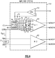
- FIG 1A is a schematic diagram of an amplifier system 1 according to one embodiment.
- the amplifier system 1 includes a first amplifier 3, a second amplifier 4, a controllable sensing circuit 10, and a control circuit 19.
- a control circuit 19 a control circuit 19
- Figure 1A the teachings herein are applicable to amplifier systems implemented in a wide variety of ways.
- the amplifier system 1 includes an input terminal (IN) for receiving an input signal, such as input voltage.
- the amplifier system 1 further includes a load terminal (LOAD) for coupling to a DUT 2 or other load, and a measurement terminal (MEAS) for outputting a measurement signal indicating an amount of current I DUT to the DUT 2.
- the amplifier system 1 also includes a control terminal (CTL) for receiving a control signal for selecting a particular configuration or mode of the amplifier system 1.
- the control terminal corresponds to a serial interface or bus that receives digital data indicating the desired configuration.
- controllable sensing circuit 10 includes a resistor 5, a capacitor 6, an integration reset switch 7, a first resistor selection switch 11, a second resistor selection switch 12, a first capacitor selection switch 13, and a second capacitor selection switch 14.
- a controllable sensing circuit such as the controllable sensing circuit 10 of Figure 1A , is also referred to herein as a configurable impedance circuit or a configurable current detection circuit.
- the control circuit 19 controls a state of the controllable sensing circuit 10.
- the control circuit 19 can selectively couple the resistor 5 between the output of the amplifier 3 and the load terminal by opening or closing the first resistor selection switch 11 and the second resistor selection switch 12.
- the control circuit 19 can selectively couple the capacitor 6 between the output of the amplifier 3 and the load terminal by opening or closing the first capacitor selection switch 13 and the second capacitor selection switch 14.
- the selection of the resistor 5 and/or the capacitor 6 is chosen based on the control signal received by the control circuit 19. Accordingly, sensing circuitry suitable for a particular type of DUT 2 can be selected. For instance, the current I DUT through the DUT 2 can vary based on a particular type of DUT, for instance, the amount of resistance, capacitance, and/or inductance of the DUT 2.
- resistor 5 is selected using a first pair of switches and the capacitor 6 is selected using a second pair of switches
- other selection schemes can be used in accordance with the teachings herein.
- a single switch is used for selection of the resistor 5 and/or a single switch is used for selection of the capacitor 6.
- the control circuit 19 also controls the integration reset switch 7 of the controllable sensing circuit 10.
- the integration reset switch 7 can be used to selectively reset a voltage across the capacitor 6, thereby controlling the capacitor's stored charge.
- a first shunt switch is connected to one end of the capacitor 6 and a second shunt switch is connected to a second end of the capacitor 6, and the shunt switches are selectively activated to reset the capacitor 6.
- the positive or non-inverting input (+) of the first amplifier 3 is coupled to the input terminal, and the negative or inverting input (-) is coupled to the load terminal.
- the controllable sensing circuit 10 is electrically coupled between the output of the first amplifier 3 and the inverting input of the first amplifier 3, and thus serves to provide controllable feedback to the first amplifier 3.
- the first amplifier 3 can be implemented in a wide variety of ways, including, but not limited to, using an operational amplifier.
- the input terminal to the amplifier system 1 can be controlled to set a bias voltage across the DUT 2.
- the second amplifier 4 includes a differential input coupled across the controllable sensing circuit 10 and an output that controls the measurement terminal.
- the second amplifier 4 outputs a measurement signal indicating an amount of current I DUT of the DUT 2.
- the non-inverting input of the second amplifier 4 can be coupled to the output of the first amplifier 3 and the inverting input of the second amplifier 4 can be coupled to the load terminal, or vice versa.
- the second amplifier 4 can be implemented in a wide variety of ways, including, but not limited to, using an instrumentation amplifier.
- Figure 1B is a schematic diagram of an amplifier system 21 according to another embodiment.
- the amplifier system 21 of Figure 1B includes a first amplifier 3, a second amplifier 4, a controllable sensing circuit 20, and a control circuit 29.
- a control circuit 29 a control circuit 29.
- the amplifier system 21 of Figure 1B is similar to the amplifier system 1 of Figure 1A , except the amplifier system 21 of Figure 1B illustrates an implementation in which the controllable sensing circuit 20 includes a controllable resistor 25 and a controllable capacitor 26. As shown in Figure 1B , the control circuit 29 controls an amount of resistance of the controllable resistor 25 and an amount of capacitance of the controllable capacitor 26.
- controllable resistor 25 and the controllable capacitor 26 can be implemented in a wide variety of ways.
- the controllable resistor 25 includes an array of selectable resistive elements (for instance, multiple branches of resistive elements each in series with a corresponding switch) and/or the controllable capacitor 26 includes an array of selectable capacitive elements.
- the controllable resistor 25 and/or the controllable capacitor are analog-tuned, for instance, by implementing the resistor and/or capacitor using transistors operating with controllable analog bias to achieve the desired resistance and/or capacitance values.
- Figure 1C is a schematic diagram of an amplifier system 31 according to another embodiment.
- the amplifier system 31 of Figure 1C includes a differential input/differential output amplifier 33, a first controllable sensing circuit 20a, a second controllable sensing circuit 20b, and a control circuit 39.
- a differential input/differential output amplifier 33 receives differential signals from a differential input/differential amplifier 33 and a control circuit 39.
- the amplifier system 31 of Figure 1C illustrates one embodiment of an amplifier system in which a pair of controllable sensing circuits are included for differential operation. Although one embodiment of a differential implementation of controllable sensing circuits is shown, any of the embodiments herein can be implemented with differential controllable sensing circuits.
- the first controllable sensing circuit 20a is electrically coupled between a non-inverting output and an inverting input of the differential input/differential output amplifier 33.
- the second controllable sensing circuit 20b is electrically coupled between an inverting output and a non-inverting input of the differential input/differential output amplifier 33.
- the inverting input of the differential input/differential output amplifier 33 is coupled to a first load terminal (LOADP), while the non-inverting input of the differential input/differential output amplifier 33 is coupled to a second load terminal (LOADN).
- a DUT can be coupled in a wide variety of ways to the first and second load terminals.
- a DUT is coupled between the first load terminal and the second load terminal for measurement.
- other configurations are possible, such as implementations in which a first DUT is coupled between the first load terminal and a reference voltage (for instance, ground) and a second DUT is coupled between the second load terminal and the reference voltage.
- an additional amplifier for generating a measurement signal is omitted in favor of generating a measurement signal using the differential input/differential output amplifier 33.
- one or more additional amplifiers are included for generating measurement signals indicating signaling conditions of a DUT.
- the first controllable sensing circuit 20a and the second controllable sensing circuit 20b are implemented in accordance with the controllable sensing circuit 20 of Figure 1B .
- the first controllable sensing circuit 20a includes a controllable resistor 25a, a controllable capacitor 26a, a integration reset switch 7a, a first resistor selection switch 11a, a second resistor selection switch 12a, a first capacitor selection switch 13a, and a second capacitor selection switch 14a.
- the second controllable sensing circuit 20b includes a controllable resistor 25b, a controllable capacitor 26b, a integration reset switch 7b, a first resistor selection switch 11b, a second resistor selection switch 12b, a first capacitor selection switch 13b, and a second capacitor selection switch 14b.
- controllable sensing circuitry Although the amplifier system 31 is illustrated with a specific implementation of controllable sensing circuitry, the teachings herein are applicable to amplifier systems using a wide range of controllable sensing circuits.
- controllable resistors 25a-25b and/or controllable capacitors 26a-26b are omitted in favor of using fixed resistor and/or capacitor components.
- control circuit 39 controls the configuration or mode of the first controllable sensing circuit 20a and the second controllable sensing circuit 20b based on a control signal received from the control terminal (CTL). Accordingly, sensing circuitry suitable for a particular type of DUT can be selected.
- FIG. 2 is a schematic diagram of an amplifier system 51 according to another embodiment.
- the amplifier system 51 includes a controllable sensing circuit 20, an operational amplifier 53, an instrumentation amplifier 61, a first feedback switch 75, a second feedback switch 76, and a control circuit 79.
- the amplifier system 51 of Figure 2 is similar to the amplifier system 21 of Figure 1B , except that the amplifier system 51 further includes the first feedback switch 75 and the second feedback switch 76, and is implemented with specific implementations of amplifiers and control circuitry.
- the amplifier system 51 includes the operational amplifier 53 for driving the DUT 2 based on the input signal received from the input terminal (IN). Including the operational amplifier 53 provides a number of advantages, such as high gain, low DC error, and/or stability over a range of operating scenarios. Additionally, the amplifier system 51 includes the instrumentation amplifier 61 for generating a differential measurement signal between a non-inverted measurement terminal (MEASP) and an inverted measurement terminal (MEASN). Including the instrumentation amplifier 61 provides a number of advantages, including, but not limited to, relaxed constraints on input impedance matching and/or enhanced measurement accuracy. Although an example with a differential measurement signal is shown, other implementations are possible.
- MEASP non-inverted measurement terminal
- MEASN inverted measurement terminal
- the first feedback switch 75 and/or the second feedback switch 76 enhances the flexibility of the amplifier system 51 relative to the amplifier system 21 of Figure 1B .
- including the first feedback switch 75 allows the control circuit 79 to selectively provide local feedback between the output and inverting input of the operational amplifier 53.
- the amplifier system 51 further includes a feedback impedance (for instance, a controllable resistor and/or a controllable capacitor) in series with the first feedback switch 75.
- the second feedback switch 76 is coupled between the load terminal (LOAD) and the inverting input of the operational amplifier 53.
- the second feedback switch 51 can be activated to provide feedback from the load terminal rather than directly from the output of the operational amplifier 53.
- Such feedback can be used to provide accurate control of a voltage of the load terminal based on a voltage of the input terminal.
- the amplifier system 51 further includes a feedback impedance (for instance, a controllable resistor and/or a controllable capacitor) in series with the second feedback switch 76.
- control circuit 79 includes a memory circuit 80 and a reset switching control circuit 81.
- the memory circuit 80 includes digital data indicating a particular configuration of the amplifier system 51. Additionally, the memory circuit 80 receives digital data from the control terminal CTL, which in certain implementations corresponds to a chip interface or bus.
- the memory circuit 80 includes a volatile memory that is programmed with the desired configuration of the amplifier system 51 using the control signal after power-up. For instance, a user of the amplifier system 51 can program the memory circuit 80 with data indicating the desired configuration of the amplifier system 51.
- the memory circuit 80 includes a non-volatile memory (for instance, a flash memory, a read-only memory (ROM), fuses, anti-fuses, and/or a magnetic storage device) programmed with the configuration data.
- the memory circuit 80 can be programmed after manufacture with data associated with a particular target application or DUT.
- the reset switching control circuit 81 controls switching operations of the integration reset switch 7, thereby controlling when the voltage across the programmable capacitor 26 is reset. For example, in certain implementations, the reset switching control circuit 81 periodically closes the integration reset switch 7 with a desired period of reset switching (T R ). In certain implementations, the timing of the integration reset switch 7 (for instance, the period of reset switching) is selected using digital data received from the control terminal (CTL) and/or stored in the memory circuit 80.
- CTL control terminal
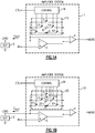
- Figures 3A-3D illustrate various example configurations or modes of operation of the amplifier system 51 of Figure 2 .
- the control circuit 79 of Figure 2 and associated control signaling is not depicted.
- the amplifier system 51 can be configured in a wide variety of ways and/or operate with a wide variety of types of DUTs. Accordingly, other implementations are possible.
- Figure 3A is a schematic diagram illustrating a first example configuration 110 of operation of the amplifier system 51 of Figure 2 .
- the first resistor selection switch 11, the second resistor selection switch 12, and the first feedback switch 75 are closed, while the integration reset switch 7, the first capacitor selection switch 13, the second capacitor selection switch 14, and the second feedback switch 76 are opened. Additionally, the resistance of the controllable resistor 25 is controlled to a desired value using the control circuit 79 of Figure 2 .
- the operational amplifier 53 is configured as a unity-gain buffer or follower, in this example. Additionally, the current I DUT of the DUT 2 is converted to a voltage through the resistor 25. The instrumentation amplifier 61 amplifies the voltage differential across the resistor 25 to generate a differential measurement signal indicating an amount of measured current of the DUT 2.
- Figure 3B is a schematic diagram illustrating a second example configuration 120 of operation of the amplifier system 51 of Figure 2 .
- the first resistor selection switch 11, the second resistor selection switch 12, and the second feedback switch 76 are closed, while the integration reset switch 7, the first capacitor selection switch 13, the second capacitor selection switch 14, and the first feedback switch 75 are opened. Additionally, the resistance of the controllable resistor 25 is controlled to a desired value using the control circuit 79 of Figure 2 .
- the operational amplifier 53 is configured as a resistive transimpedance amplifier. Additionally, since the second feedback switch 76 is closed, the operational amplifier 53 biases the DUT 2 with a bias voltage corresponding to an input voltage of the input terminal (IN). Furthermore, the current I DUT of the DUT 2 is converted to a voltage through the resistor 25 with a gain based on the resistor's selected resistance. The instrumentation amplifier 61 amplifies the voltage differential across the resistor 25 to generate a differential measurement signal indicating an amount of measured current of the DUT 2.
- Configuring an amplifier system to operate as a resistive transimpedance amplifier can be desirable for a wide variety of applications, such as when measuring a large amount of current.
- a large value capacitor and/or a high clock rate of a reset integration switch may be needed to avoid saturating the capacitor.
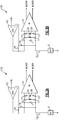
- Figure 3C is a schematic diagram illustrating a third example configuration 130 of operation of the amplifier system 51 of Figure 2 .
- the first resistor selection switch 11, the second resistor selection switch 12, the first capacitor selection switch 13, the second capacitor selection switch 14, and the second feedback switch 76 are closed, while the integration reset switch 7 and the first feedback switch 75 are opened. Additionally, the resistance of the controllable resistor 25 and the capacitance of the controllable capacitor 26 are controlled to desired values using the control circuit 79 of Figure 2 .
- the operational amplifier 53 is configured as a resistive transimpedance amplifier. Additionally, the current I DUT of the DUT 2 is converted to a voltage through the resistor 25 with a gain based on the resistor's selected resistance. Furthermore, the instrumentation amplifier 61 amplifies the voltage differential across the resistor 25 to generate a differential measurement signal indicating an amount of measured current of the DUT 2.
- the capacitor 26 is also selected in this configuration, and serves to provide frequency compensation or stability to the transimpedance amplifier 61 and/or to limit a bandwidth of the transimpedance amplifier 61.
- Figure 3D is a schematic diagram illustrating a fourth example configuration 140 of operation of the amplifier system 51 of Figure 2 .
- the first capacitor selection switch 13, the second capacitor selection switch 14, and the second feedback switch 76 are closed, while the first resistor selection switch 11, the second resistor selection switch 12, and the first feedback switch 75 are opened. Additionally, the capacitance of the controllable capacitor 26 is controlled to a desired value using the control circuit 79 of Figure 2 .
- the integration reset switch 7 is depicted as opened, but is selectively closed (for instance, with a desired period of reset switching) by the control circuit 79 of Figure 2 . In certain implementations, the timing of the integration reset switch 7 (for instance, the period of reset switching) is selected using digital data received from the control terminal (CTL) of Figure 2 .
- the operational amplifier 53 is configured as a capacitive transimpedance amplifier. Additionally, the current I DUT of the DUT 2 is integrated onto the capacitor 26, with the integration reset switch 7 selectively closed as desired (for instance, periodically based on a period of reset switching) to reset the charge on the capacitor 26. Furthermore, the instrumentation amplifier 61 amplifies the voltage across the across the capacitor 26 to generate a differential measurement signal indicating an amount of measured current of the DUT 2.
- Configuring an amplifier system to operate as a capacitive transimpedance amplifier can be desirable for a wide variety of applications, such as when measuring a small amount of current to avoid a need for using a large value resistor.
- FIG 4 is a schematic diagram of an amplifier system 151 according to another embodiment.
- the amplifier system 151 of Figure 4 is similar to the amplifier system 51 of Figure 2 , except that the amplifier system 151 further includes a second instrumentation amplifier 62.
- the amplifier system 151 not only includes the first instrumentation amplifier 61 for generating a first differential measurement signal between a first non-inverted measurement terminal (MEAS 1P) and a first inverted measurement terminal (MEAS 1N), but also the second instrumentation amplifier 62 for generating a second differential measurement signal between a second non-inverted measurement terminal (MEAS2P) and a second inverted measurement terminal (MEAS2N).
- the first differential measurement signal from the first instrumentation amplifier 61 indicates an amount of current I DUT of the DUT 2 as measured by the amplifier system 151.
- the second instrumentation amplifier 62 amplifies a voltage across the DUT 2 to generate the second differential measurement signal, and thus the second differential measurement signal indicates a bias voltage of the DUT 2.
- the second instrumentation amplifier 62 By including the second instrumentation amplifier 62, a voltage across the DUT 2 is measured. Thus, the second differential measurement signal can be processed to monitor the DUT's bias voltage.
- the second instrumentation amplifier 62 is connected to the input terminal (IN) through a feedback loop that enhances an accuracy of biasing and/or protects the DUT 2 from overvoltage and/or other undesired biasing conditions.
- the second instrumentation amplifier 62 includes a first input coupled to a feedback input terminal (FBIN) and a second input coupled to a ground terminal (GND), which in turn are coupled to a first terminal and a second terminal, respectively, of the DUT 2.
- FBIN feedback input terminal
- GND ground terminal
- amplifiers and controllable sensing circuitry Although an embodiment with specific types of amplifiers and controllable sensing circuitry is shown, the teachings herein are applicable to amplifier systems using a wide variety of types of amplifiers and/or controllable sensing circuits. Furthermore, although certain signals are indicated as single-ended or differential, the amplifier systems herein can use a wide variety of types of signaling.
- FIG. 5A is a schematic diagram of one embodiment of an electronic system 200 including an amplifier system controlled by processing.
- the electronic system 200 includes an amplifier system 201, a DUT 2, and a processing system 203.
- the amplifier system 201 includes an input terminal (IN) that receives an input signal from the processing system 203. Additionally, the amplifier system 201 includes a load terminal (LOAD) for coupling to the DUT 2, and a control terminal (CTL) for receiving a control signal for configuring the amplifier system 201.
- the amplifier system 201 can be implemented in accordance with any of the embodiments herein.
- the processing system 203 receives one or more measurement signals indicating a signaling condition of the DUT 2. Additionally, the processing system 203 processes the measurement signal(s) using desired processing operations. In certain implementations, the processing system 203 controls the input signal to the amplifier system 201 based on the measurement signal(s). Thus, the processing system 203 can be used to control feedback.
- Figure 5A illustrates one embodiment of an amplifier system with processing
- teachings herein are applicable to amplifier systems implemented in a wide variety of ways.
- Figure 5B is a schematic diagram of another embodiment of an electronic system 210 including an amplifier system controlled by processing.
- the electronic system 210 of Figure 5B is similar to the electronic system 200 of Figure 5A , except that the electronic system 210 includes a specific implementation of an amplifier system and of a processing system.
- the electronic system 210 of Figure 5B has been implemented with the amplifier system 151 described above with respect to Figure 4 .
- the electronic system 210 includes a processing system 213 that includes a first ADC 221, a second ADC 222, a digital processing circuit 223, and a DAC 224.
- the first ADC 221 digitizes the first measurement signal from the first instrumentation amplifier 61 to generate a first digital measurement signal for the digital processing circuit 223.
- the second ADC 222 digitizes the second measurement signal from the second instrumentation amplifier 62 to generate a second digital measurement signal for the digital processing circuit 223.
- the digital processing circuit 223 generates digital output data, which the DAC 224 processes to control the input signal to the amplifier system 151.
- the digital output data is generated based on processing the first digital measurement signal and/or the second digital measurement signal.
- first digital feedback 227 can be provided based on the first digital measurement signal and/or second digital feedback 228 can be provided based on the second digital measurement signal.
- the processing system 213 can provide digital integration, digital gain, and/or other desired digital processing to provide a type and/or an amount of feedback desirable for a particular configuration of the amplifier system 151 selected for a particular usage scenario.
- the digital processing circuit 223 can be implemented in a wide variety of ways.
- the digital processing circuit 223 includes at least one of an FPGA and/or microprocessor for providing a wide variety of types of digital processing.
- FIG. 6 is a schematic diagram of a multi-chip module 310 according to one embodiment.
- the multi-chip module 310 includes a processing chip 303 and an amplifier chip 304 connected to a module substrate 301.
- a chip is also referred to herein as a semiconductor die or integrated circuit (IC).
- IC integrated circuit
- the multi-chip module 310 can also include adhesives, solder, encapsulation, surface mount components, additional pins or pads, and/or a wide variety of other structures that have been omitted for clarity of the figures.
- the multi-chip module 310 illustrates one example of an electronic module implemented in accordance with the teachings herein.
- the processing chip 303 includes the first ADC 221, the second ADC 222, the digital processing circuit 223, and the DAC 224 fabricated thereon.
- the amplifier chip 304 includes the amplifier system 305 fabricated thereon.
- the amplifier system 305 can be implemented in accordance with any of the embodiments herein.
- the amplifier chip 304 includes an input pin for receiving an input signal from the processing chip 303, and a load pin for coupling to the sensor 302 through a load pin of the multi-chip module 310.
- the amplifier chip 304 also includes a feedback input pin and a ground pin for receiving a differential feedback signal through corresponding pins of the module.
- the differential feedback signal corresponds to a voltage across the sensor 302.
- the multi-chip module 310 includes an interface or bus (BUS) that is coupled through pins of the dies to the digital processing circuit 223 and amplifier system 305.
- the bus can be used to program digital data to the processing chip 303 and amplifier chip 304 to achieve a desired configuration of the multi-chip module 310 for a given sensor 302.
- the processing IC 303 corresponds to an FPGA and/or microprocessor operable to receive digital data from the bus to control the type of processing computations performed. Such computations can include, but are not limited to, digital control of feedback.
- the load pin (LOAD) of the multi-chip module 310 couples to a first terminal of the sensor 302.
- the feedback input pin (FBIN) of the multi-chip module 310 also couples to the first terminal of the sensor 302.
- the multi-chip module 310 also includes a ground pin (GND) coupled to a second terminal of the sensor 302.
- GND ground pin
- the multi-chip module 310 of Figure 6 is suitable for deployment in a wide range of applications.
- the multi-chip module 310 can operate in combination with a wide variety of types of sensors, including sensors with varying impedances and/or biasing conditions.
- a multi-chip module is shown, the teachings herein are applicable to a wide variety of types of electronic systems and modules. Accordingly, other implementations are possible.
Landscapes
- Physics & Mathematics (AREA)
- General Physics & Mathematics (AREA)
- Engineering & Computer Science (AREA)
- Power Engineering (AREA)
- Amplifiers (AREA)
Abstract
Description
- The present application claims priority to
U.S. Provisional Patent Application No. 62/746,726, filed October 17,2018 - Embodiments of the invention relate to electronic systems, and more particularly, to amplifiers.
- Certain electronic devices employ amplifiers for processing signals. When operating open loop, such amplifiers receive an input signal and generate an output signal having a gain in comparison to the input signal. Examples of amplifiers include, but are not limited to, operational amplifiers, transimpedance amplifiers, and transconductance amplifiers. Certain amplifiers are implemented in a multi-stage configuration to enhance gain and/or performance thereof.
- Amplifier systems for measuring a wide range of current are provided herein. In certain embodiments, an amplifier system includes a controllable sensing circuit, a first amplifier including an output configured to drive a device under test (DUT) through the controllable sensing circuit, and a second amplifier including an input coupled to the controllable sensing circuit and operable to generate a measurement signal indicating an amount of measured current of the DUT. The amplifier system further includes a control circuit operable to control a configuration or mode of the controllable sensing circuit suitable for a particular type of DUT. Implementing the amplifier system in this manner allows measurement of a wide range of current from a variety of DUTs. For instance, the amplifier system can operate as a reconfigurable analog front-end (AFE) suitable for measuring a range of current spanning multiple decades for DUTs having various impedances. For example, the controllable sensing circuit can include resistors, capacitors, and/or other selectable and/or controllable components to thereby provide configurability for different types of loads, such as DUTs of a range of different impedance values.
- In one aspect, an amplifier system with controllable current measurement characteristics is provided. The amplifier system includes a load terminal configured to output a current to a DUT, a controllable sensing circuit, a first amplifier including an output electrically connected to the load terminal through the controllable sensing circuit, a second amplifier including an input coupled to the controllable sensing circuit, and a control circuit operable to control an impedance of the controllable sensing circuit. The second amplifier is operable to generate a measurement signal indicating a detected amount of the current outputted from the load terminal.
- In another aspect, an electronic module with controllable current measurement characteristics is provided. The electronic module includes a module substrate, and an amplifier die attached to the module substrate. The amplifier die includes a load pin configured to output a current, a first amplifier, a controllable sensing circuit electrically connected between an output of the first amplifier and the load pin, a second amplifier including a first input electrically connected to the output of the first amplifier and a second input electrically connected to the load pin, the second amplifier operable to generate a measurement signal indicating a detected amount of the current outputted from the load pin, and a control circuit operable to control an impedance of the controllable sensing circuit.
- In another aspect, a method of controllable current measurement in an amplifier system is provided. The method includes controlling an impedance of a controllable sensing circuit using a control circuit, providing a current from an output terminal to a DUT, driving the output terminal through the controllable sensing circuit using a first amplifier, generating a voltage across the controllable sensing circuit in response to the current, and generating a measurement signal based on amplifying the voltage across the controllable sensing circuit using a second amplifier so as to measure the current.
- In another aspect, an amplifier system with controllable current measurement characteristics is provided. The amplifier system includes a first load terminal and a second load terminal, an amplifier including an inverting input electrically connected to the first load terminal and a non-inverting input electrically connected to the second load terminal, a first controllable sensing circuit electrically connected between a non-inverting output of the amplifier and the inverting input of the amplifier, a second controllable sensing circuit electrically connected between an inverting output of the amplifier and the non-inverting input of the amplifier, and a control circuit operable to control an impedance of the first controllable sensing circuit and an impedance of the second controllable sensing circuit.
-
-
Figure 1A is a schematic diagram of an amplifier system according to one embodiment. -
Figure 1B is a schematic diagram of an amplifier system according to another embodiment. -
Figure 1C is a schematic diagram of an amplifier system according to another embodiment. -
Figure 2 is a schematic diagram of an amplifier system according to another embodiment. -
Figure 3A is a schematic diagram illustrating a first example configuration of operation of the amplifier system ofFigure 2 . -
Figure 3B is a schematic diagram illustrating a second example configuration of operation of the amplifier system ofFigure 2 . -
Figure 3C is a schematic diagram illustrating a third example configuration of operation of the amplifier system ofFigure 2 . -
Figure 3D is a schematic diagram illustrating a fourth example configuration of operation of the amplifier system ofFigure 2 . -
Figure 4 is a schematic diagram of an amplifier system according to another embodiment. -
Figure 5A is a schematic diagram of one embodiment of an electronic system including an amplifier system controlled by processing. -
Figure 5B is a schematic diagram of another embodiment of an electronic system including an amplifier system controlled by processing. -
Figure 6 is a schematic diagram of a multi-chip module according to one embodiment. - The following detailed description of embodiments presents various descriptions of specific embodiments of the invention. However, the invention can be embodied in a multitude of different ways. In this description, reference is made to the drawings where like reference numerals may indicate identical or functionally similar elements. It will be understood that elements illustrated in the figures are not necessarily drawn to scale. Moreover, it will be understood that certain embodiments can include more elements than illustrated in a drawing and/or a subset of the elements illustrated in a drawing. Further, some embodiments can incorporate any suitable combination of features from two or more drawings.
- Amplifier systems for measuring a wide range of current are provided herein. In certain embodiments, an amplifier system includes a controllable sensing circuit, a first amplifier including an output configured to drive a device under test (DUT) through the controllable sensing circuit, and a second amplifier including an input coupled to the controllable sensing circuit and operable to generate a measurement signal indicating an amount of current flowing to the DUT. The amplifier system further includes a control circuit operable to control a configuration or mode of the controllable sensing circuit suitable for measuring the current of a particular type of DUT.
- Implementing the amplifier system in this manner allows measurement of a wide range of current from a variety of DUTs. For instance, the amplifier system can operate as a reconfigurable analog front-end (AFE) suitable for measuring a range of current spanning multiple decades for DUTs having various impedances. For example, the controllable sensing circuit can include resistors, capacitors, and/or other selectable and/or controllable components to thereby provide configurability for different types of loads, such as DUTs of a range of different impedance values.
- In certain implementations, the controllable sensing circuit is connectable between the output of the first amplifier and an inverting input to the first amplifier, thereby controlling an amount of feedback provided to the first amplifier. For instance, an amount of resistive and/or capacitive feedback to the first amplifier can be controlled to achieve desired operating characteristics for a particular DUT and/or application.
- Thus, enhanced flexibility of the amplifier system is provided for measuring current from a wide range of possible types of DUTs or loads. Thus, rather than needing a dedicated part (for instance, a particular chip design) for a particular type of DUT, the amplifier systems herein can be incorporated on a semiconductor chip suitable for measuring current from DUTs of a range of different impedances.
- In certain implementations, the first amplifier is implemented as an operational amplifier, such as a multi-stage operational amplifier that drives the DUT through the controllable sensing circuit. In certain implementations, the second amplifier is implemented as an instrumentation amplifier, thereby relaxing constraints on input impedance matching and/or providing enhanced measurement accuracy.
- The amplifier systems herein operate stably when connected with negative feedback. For example, the controllable sensing circuit can also be configured to provide feedback and/or compensation to maintain stability. In contrast, an amplifier system without such configurability can exhibit oscillation and/or other unstable behavior under certain load conditions.
- To further enhance configurability, the amplifier system can be implemented with switches for selectively providing local feedback to the first amplifier.
- In certain implementations, the amplifier system is coupled to an interface or bus, such as an inter-Integrated Circuit (I2C) bus, a General Purpose Input Output (GPIO) bus, and/or other suitable interface. Additionally, the amplifier system's control circuit receives digital data from the bus used to control a configuration or setting of the amplifier system. For example, the amplifier system can be fabricated on a semiconductor die or chip, and a user can digitally program a desired configuration or mode of the controllable sensing circuit using the bus. Implementing the amplifier system in this manner provides a convenient and flexible mechanism for user configurability.
- The amplifier systems herein can be used in a wide range of applications, including, but not limited to, current measurement of sensors. For example, an amplifier system can be used to measure a sensor's current, thereby detecting various changes in environmental quantities or conditions. In certain implementations, the amplifier system also biases the sensor and/or measures a sensor's bias voltage to aid in enhancing measurement accuracy and/or to protect the sensor from damage from overvoltage or other improper biasing.
- In certain implementations, a processing system is included for controlling an input to the first amplifier. For example, the processing system can control a bias voltage of the DUT by setting a signal level to the non-inverting input of the first amplifier. In certain implementations, the processing system processes the measurement signal from the second amplifier and/or other measurement signals to control the input signal level to the first amplifier. Accordingly, the processing system can operate in a feedback loop.
- The processing system can be implemented in a wide variety of ways. In one example, the processing system includes an analog-to-digital converter (ADC) for generating digital input data based on the measurement signal, a digital processing circuit for processing the digital input data to generate digital output data, and a digital-to-analog converter (DAC) for controlling the input signal to the first amplifier based on the digital output data.
- Implementing the processing system in this manner can provide a number of advantages, including, but not limited to, enhanced flexibility in control of feedback over a range of different configurations of the amplifier system. For example, the digital processing circuit can provide digital integration, digital gain, and/or other desired digital processing to provide a type of feedback desirable for a particular configuration of the amplifier system chosen for a given application and/or type of DUT.
- In certain implementations, a processing chip, such as a field-programmable gate array (FPGA) and/or microprocessor, is commonly packaged with an amplifier chip in a multi-chip module. The amplifier chip can include the configurable amplifier system thereon and generate at least one feedback signal based on monitoring signaling conditions of a DUT, such as a sensor external to the multi-chip module. Additionally, the analog feedback signal(s) are processed by the processing chip to generate an input signal for the amplifier chip. Such multi-chip modules are suitable for deployment in a wide range of applications.
-
Figure 1A is a schematic diagram of anamplifier system 1 according to one embodiment. Theamplifier system 1 includes afirst amplifier 3, a second amplifier 4, a controllable sensing circuit 10, and acontrol circuit 19. Although one embodiment of an amplifier system is shown inFigure 1A , the teachings herein are applicable to amplifier systems implemented in a wide variety of ways. - With continuing reference to
Figure 1A , theamplifier system 1 includes an input terminal (IN) for receiving an input signal, such as input voltage. Theamplifier system 1 further includes a load terminal (LOAD) for coupling to aDUT 2 or other load, and a measurement terminal (MEAS) for outputting a measurement signal indicating an amount of current IDUT to theDUT 2. Theamplifier system 1 also includes a control terminal (CTL) for receiving a control signal for selecting a particular configuration or mode of theamplifier system 1. In certain implementations, the control terminal corresponds to a serial interface or bus that receives digital data indicating the desired configuration. - In the illustrated embodiment, the controllable sensing circuit 10 includes a
resistor 5, a capacitor 6, anintegration reset switch 7, a firstresistor selection switch 11, a secondresistor selection switch 12, a firstcapacitor selection switch 13, and a secondcapacitor selection switch 14. Although one embodiment of a controllable sensing circuit is shown, the teachings herein are applicable to controllable sensing circuits implemented in a wide variety of ways. A controllable sensing circuit, such as the controllable sensing circuit 10 ofFigure 1A , is also referred to herein as a configurable impedance circuit or a configurable current detection circuit. - As shown in
Figure 1A , thecontrol circuit 19 controls a state of the controllable sensing circuit 10. In this embodiment, thecontrol circuit 19 can selectively couple theresistor 5 between the output of theamplifier 3 and the load terminal by opening or closing the firstresistor selection switch 11 and the secondresistor selection switch 12. Additionally, thecontrol circuit 19 can selectively couple the capacitor 6 between the output of theamplifier 3 and the load terminal by opening or closing the firstcapacitor selection switch 13 and the secondcapacitor selection switch 14. - The selection of the
resistor 5 and/or the capacitor 6 is chosen based on the control signal received by thecontrol circuit 19. Accordingly, sensing circuitry suitable for a particular type ofDUT 2 can be selected. For instance, the current IDUT through theDUT 2 can vary based on a particular type of DUT, for instance, the amount of resistance, capacitance, and/or inductance of theDUT 2. - Although an example in which the
resistor 5 is selected using a first pair of switches and the capacitor 6 is selected using a second pair of switches, other selection schemes can be used in accordance with the teachings herein. For instance, in another embodiment, a single switch is used for selection of theresistor 5 and/or a single switch is used for selection of the capacitor 6. - The
control circuit 19 also controls theintegration reset switch 7 of the controllable sensing circuit 10. The integration resetswitch 7 can be used to selectively reset a voltage across the capacitor 6, thereby controlling the capacitor's stored charge. Although one example configuration for resetting the capacitor 6 is shown, other implementations are possible. For instance, in another implementation a first shunt switch is connected to one end of the capacitor 6 and a second shunt switch is connected to a second end of the capacitor 6, and the shunt switches are selectively activated to reset the capacitor 6. - As shown in
Figure 1A , the positive or non-inverting input (+) of thefirst amplifier 3 is coupled to the input terminal, and the negative or inverting input (-) is coupled to the load terminal. In the illustrated embodiment, the controllable sensing circuit 10 is electrically coupled between the output of thefirst amplifier 3 and the inverting input of thefirst amplifier 3, and thus serves to provide controllable feedback to thefirst amplifier 3. Thefirst amplifier 3 can be implemented in a wide variety of ways, including, but not limited to, using an operational amplifier. In this example, the input terminal to theamplifier system 1 can be controlled to set a bias voltage across theDUT 2. - In the illustrated embodiment, the second amplifier 4 includes a differential input coupled across the controllable sensing circuit 10 and an output that controls the measurement terminal. The second amplifier 4 outputs a measurement signal indicating an amount of current IDUT of the
DUT 2. The non-inverting input of the second amplifier 4 can be coupled to the output of thefirst amplifier 3 and the inverting input of the second amplifier 4 can be coupled to the load terminal, or vice versa. The second amplifier 4 can be implemented in a wide variety of ways, including, but not limited to, using an instrumentation amplifier. -
Figure 1B is a schematic diagram of anamplifier system 21 according to another embodiment. Theamplifier system 21 ofFigure 1B includes afirst amplifier 3, a second amplifier 4, acontrollable sensing circuit 20, and acontrol circuit 29. Although another embodiment of an amplifier system is shown inFigure 1B , the teachings herein are applicable to amplifier systems implemented in a wide variety of ways. - The
amplifier system 21 ofFigure 1B is similar to theamplifier system 1 ofFigure 1A , except theamplifier system 21 ofFigure 1B illustrates an implementation in which thecontrollable sensing circuit 20 includes acontrollable resistor 25 and acontrollable capacitor 26. As shown inFigure 1B , thecontrol circuit 29 controls an amount of resistance of thecontrollable resistor 25 and an amount of capacitance of thecontrollable capacitor 26. - The
controllable resistor 25 and thecontrollable capacitor 26 can be implemented in a wide variety of ways. In one example, thecontrollable resistor 25 includes an array of selectable resistive elements (for instance, multiple branches of resistive elements each in series with a corresponding switch) and/or thecontrollable capacitor 26 includes an array of selectable capacitive elements. In another example, thecontrollable resistor 25 and/or the controllable capacitor are analog-tuned, for instance, by implementing the resistor and/or capacitor using transistors operating with controllable analog bias to achieve the desired resistance and/or capacitance values. Although various examples of controllable resistors and capacitors have been described, other implementations of controllable elements are possible. -
Figure 1C is a schematic diagram of anamplifier system 31 according to another embodiment. Theamplifier system 31 ofFigure 1C includes a differential input/differential output amplifier 33, a firstcontrollable sensing circuit 20a, a secondcontrollable sensing circuit 20b, and acontrol circuit 39. Although another embodiment of an amplifier system is shown inFigure 1C , the teachings herein are applicable to amplifier systems implemented in a wide variety of ways. - The
amplifier system 31 ofFigure 1C illustrates one embodiment of an amplifier system in which a pair of controllable sensing circuits are included for differential operation. Although one embodiment of a differential implementation of controllable sensing circuits is shown, any of the embodiments herein can be implemented with differential controllable sensing circuits. - In the illustrated embodiment, the first
controllable sensing circuit 20a is electrically coupled between a non-inverting output and an inverting input of the differential input/differential output amplifier 33. Additionally, the secondcontrollable sensing circuit 20b is electrically coupled between an inverting output and a non-inverting input of the differential input/differential output amplifier 33. As shown inFigure 1C , the inverting input of the differential input/differential output amplifier 33 is coupled to a first load terminal (LOADP), while the non-inverting input of the differential input/differential output amplifier 33 is coupled to a second load terminal (LOADN). - A DUT can be coupled in a wide variety of ways to the first and second load terminals. In certain implementation, a DUT is coupled between the first load terminal and the second load terminal for measurement. However, other configurations are possible, such as implementations in which a first DUT is coupled between the first load terminal and a reference voltage (for instance, ground) and a second DUT is coupled between the second load terminal and the reference voltage.
- In the illustrated embodiment, an additional amplifier for generating a measurement signal is omitted in favor of generating a measurement signal using the differential input/
differential output amplifier 33. In other embodiments, one or more additional amplifiers are included for generating measurement signals indicating signaling conditions of a DUT. - As shown in
Figure 1C , the firstcontrollable sensing circuit 20a and the secondcontrollable sensing circuit 20b are implemented in accordance with thecontrollable sensing circuit 20 ofFigure 1B . For example, the firstcontrollable sensing circuit 20a includes a controllable resistor 25a, acontrollable capacitor 26a, a integration reset switch 7a, a first resistor selection switch 11a, a secondresistor selection switch 12a, a firstcapacitor selection switch 13a, and a secondcapacitor selection switch 14a. Additionally, the secondcontrollable sensing circuit 20b includes acontrollable resistor 25b, acontrollable capacitor 26b, aintegration reset switch 7b, a first resistor selection switch 11b, a secondresistor selection switch 12b, a firstcapacitor selection switch 13b, and a secondcapacitor selection switch 14b. - Although the
amplifier system 31 is illustrated with a specific implementation of controllable sensing circuitry, the teachings herein are applicable to amplifier systems using a wide range of controllable sensing circuits. In another embodiment, the controllable resistors 25a-25b and/orcontrollable capacitors 26a-26b are omitted in favor of using fixed resistor and/or capacitor components. - As shown in
Figure 1C , thecontrol circuit 39 controls the configuration or mode of the firstcontrollable sensing circuit 20a and the secondcontrollable sensing circuit 20b based on a control signal received from the control terminal (CTL). Accordingly, sensing circuitry suitable for a particular type of DUT can be selected. -
Figure 2 is a schematic diagram of anamplifier system 51 according to another embodiment. Theamplifier system 51 includes acontrollable sensing circuit 20, anoperational amplifier 53, aninstrumentation amplifier 61, afirst feedback switch 75, asecond feedback switch 76, and acontrol circuit 79. - The
amplifier system 51 ofFigure 2 is similar to theamplifier system 21 ofFigure 1B , except that theamplifier system 51 further includes thefirst feedback switch 75 and thesecond feedback switch 76, and is implemented with specific implementations of amplifiers and control circuitry. - For example, in this embodiment, the
amplifier system 51 includes theoperational amplifier 53 for driving theDUT 2 based on the input signal received from the input terminal (IN). Including theoperational amplifier 53 provides a number of advantages, such as high gain, low DC error, and/or stability over a range of operating scenarios. Additionally, theamplifier system 51 includes theinstrumentation amplifier 61 for generating a differential measurement signal between a non-inverted measurement terminal (MEASP) and an inverted measurement terminal (MEASN). Including theinstrumentation amplifier 61 provides a number of advantages, including, but not limited to, relaxed constraints on input impedance matching and/or enhanced measurement accuracy. Although an example with a differential measurement signal is shown, other implementations are possible. - With continuing reference to
Figure 2 , including thefirst feedback switch 75 and/or thesecond feedback switch 76 enhances the flexibility of theamplifier system 51 relative to theamplifier system 21 ofFigure 1B . For example, including thefirst feedback switch 75 allows thecontrol circuit 79 to selectively provide local feedback between the output and inverting input of theoperational amplifier 53. In certain implementations, theamplifier system 51 further includes a feedback impedance (for instance, a controllable resistor and/or a controllable capacitor) in series with thefirst feedback switch 75. - The
second feedback switch 76 is coupled between the load terminal (LOAD) and the inverting input of theoperational amplifier 53. Thus, thesecond feedback switch 51 can be activated to provide feedback from the load terminal rather than directly from the output of theoperational amplifier 53. Such feedback can be used to provide accurate control of a voltage of the load terminal based on a voltage of the input terminal. In certain implementations, theamplifier system 51 further includes a feedback impedance (for instance, a controllable resistor and/or a controllable capacitor) in series with thesecond feedback switch 76. - In the illustrated embodiment, the
control circuit 79 includes amemory circuit 80 and a reset switchingcontrol circuit 81. Thememory circuit 80 includes digital data indicating a particular configuration of theamplifier system 51. Additionally, thememory circuit 80 receives digital data from the control terminal CTL, which in certain implementations corresponds to a chip interface or bus. - In certain implementations, the
memory circuit 80 includes a volatile memory that is programmed with the desired configuration of theamplifier system 51 using the control signal after power-up. For instance, a user of theamplifier system 51 can program thememory circuit 80 with data indicating the desired configuration of theamplifier system 51. However, other configurations are possible, such as implementations in which thememory circuit 80 includes a non-volatile memory (for instance, a flash memory, a read-only memory (ROM), fuses, anti-fuses, and/or a magnetic storage device) programmed with the configuration data. In such implementations, thememory circuit 80 can be programmed after manufacture with data associated with a particular target application or DUT. - The reset switching
control circuit 81 controls switching operations of theintegration reset switch 7, thereby controlling when the voltage across theprogrammable capacitor 26 is reset. For example, in certain implementations, the reset switchingcontrol circuit 81 periodically closes theintegration reset switch 7 with a desired period of reset switching (TR). In certain implementations, the timing of the integration reset switch 7 (for instance, the period of reset switching) is selected using digital data received from the control terminal (CTL) and/or stored in thememory circuit 80. -
Figures 3A-3D illustrate various example configurations or modes of operation of theamplifier system 51 ofFigure 2 . For clarity of the figures, thecontrol circuit 79 ofFigure 2 and associated control signaling is not depicted. Although four example configurations of operation are shown, theamplifier system 51 can be configured in a wide variety of ways and/or operate with a wide variety of types of DUTs. Accordingly, other implementations are possible. -
Figure 3A is a schematic diagram illustrating afirst example configuration 110 of operation of theamplifier system 51 ofFigure 2 . - In this example, the first
resistor selection switch 11, the secondresistor selection switch 12, and thefirst feedback switch 75 are closed, while theintegration reset switch 7, the firstcapacitor selection switch 13, the secondcapacitor selection switch 14, and thesecond feedback switch 76 are opened. Additionally, the resistance of thecontrollable resistor 25 is controlled to a desired value using thecontrol circuit 79 ofFigure 2 . - With continuing reference to
Figure 3A , theoperational amplifier 53 is configured as a unity-gain buffer or follower, in this example. Additionally, the current IDUT of theDUT 2 is converted to a voltage through theresistor 25. Theinstrumentation amplifier 61 amplifies the voltage differential across theresistor 25 to generate a differential measurement signal indicating an amount of measured current of theDUT 2. -
Figure 3B is a schematic diagram illustrating asecond example configuration 120 of operation of theamplifier system 51 ofFigure 2 . - In this example, the first
resistor selection switch 11, the secondresistor selection switch 12, and thesecond feedback switch 76 are closed, while theintegration reset switch 7, the firstcapacitor selection switch 13, the secondcapacitor selection switch 14, and thefirst feedback switch 75 are opened. Additionally, the resistance of thecontrollable resistor 25 is controlled to a desired value using thecontrol circuit 79 ofFigure 2 . - With continuing reference to
Figure 3B , theoperational amplifier 53 is configured as a resistive transimpedance amplifier. Additionally, since thesecond feedback switch 76 is closed, theoperational amplifier 53 biases theDUT 2 with a bias voltage corresponding to an input voltage of the input terminal (IN). Furthermore, the current IDUT of theDUT 2 is converted to a voltage through theresistor 25 with a gain based on the resistor's selected resistance. Theinstrumentation amplifier 61 amplifies the voltage differential across theresistor 25 to generate a differential measurement signal indicating an amount of measured current of theDUT 2. - Configuring an amplifier system to operate as a resistive transimpedance amplifier can be desirable for a wide variety of applications, such as when measuring a large amount of current. In contrast, when measuring a large current using a capacitive transimpedance amplifier, a large value capacitor and/or a high clock rate of a reset integration switch may be needed to avoid saturating the capacitor.
-
Figure 3C is a schematic diagram illustrating athird example configuration 130 of operation of theamplifier system 51 ofFigure 2 . - In this example, the first
resistor selection switch 11, the secondresistor selection switch 12, the firstcapacitor selection switch 13, the secondcapacitor selection switch 14, and thesecond feedback switch 76 are closed, while theintegration reset switch 7 and thefirst feedback switch 75 are opened. Additionally, the resistance of thecontrollable resistor 25 and the capacitance of thecontrollable capacitor 26 are controlled to desired values using thecontrol circuit 79 ofFigure 2 . - With continuing reference to
Figure 3C , theoperational amplifier 53 is configured as a resistive transimpedance amplifier. Additionally, the current IDUT of theDUT 2 is converted to a voltage through theresistor 25 with a gain based on the resistor's selected resistance. Furthermore, theinstrumentation amplifier 61 amplifies the voltage differential across theresistor 25 to generate a differential measurement signal indicating an amount of measured current of theDUT 2. Thecapacitor 26 is also selected in this configuration, and serves to provide frequency compensation or stability to thetransimpedance amplifier 61 and/or to limit a bandwidth of thetransimpedance amplifier 61. -
Figure 3D is a schematic diagram illustrating afourth example configuration 140 of operation of theamplifier system 51 ofFigure 2 . - In this example, the first
capacitor selection switch 13, the secondcapacitor selection switch 14, and thesecond feedback switch 76 are closed, while the firstresistor selection switch 11, the secondresistor selection switch 12, and thefirst feedback switch 75 are opened. Additionally, the capacitance of thecontrollable capacitor 26 is controlled to a desired value using thecontrol circuit 79 ofFigure 2 . The integration resetswitch 7 is depicted as opened, but is selectively closed (for instance, with a desired period of reset switching) by thecontrol circuit 79 ofFigure 2 . In certain implementations, the timing of the integration reset switch 7 (for instance, the period of reset switching) is selected using digital data received from the control terminal (CTL) ofFigure 2 . - With continuing reference to
Figure 3D , theoperational amplifier 53 is configured as a capacitive transimpedance amplifier. Additionally, the current IDUT of theDUT 2 is integrated onto thecapacitor 26, with theintegration reset switch 7 selectively closed as desired (for instance, periodically based on a period of reset switching) to reset the charge on thecapacitor 26. Furthermore, theinstrumentation amplifier 61 amplifies the voltage across the across thecapacitor 26 to generate a differential measurement signal indicating an amount of measured current of theDUT 2. - Configuring an amplifier system to operate as a capacitive transimpedance amplifier can be desirable for a wide variety of applications, such as when measuring a small amount of current to avoid a need for using a large value resistor.
-
Figure 4 is a schematic diagram of anamplifier system 151 according to another embodiment. Theamplifier system 151 ofFigure 4 is similar to theamplifier system 51 ofFigure 2 , except that theamplifier system 151 further includes asecond instrumentation amplifier 62. For example, theamplifier system 151 not only includes thefirst instrumentation amplifier 61 for generating a first differential measurement signal between a first non-inverted measurement terminal (MEAS 1P) and a first inverted measurement terminal (MEAS 1N), but also thesecond instrumentation amplifier 62 for generating a second differential measurement signal between a second non-inverted measurement terminal (MEAS2P) and a second inverted measurement terminal (MEAS2N). - As discussed above, the first differential measurement signal from the
first instrumentation amplifier 61 indicates an amount of current IDUT of theDUT 2 as measured by theamplifier system 151. As shown inFigure 4 , thesecond instrumentation amplifier 62 amplifies a voltage across theDUT 2 to generate the second differential measurement signal, and thus the second differential measurement signal indicates a bias voltage of theDUT 2. - By including the
second instrumentation amplifier 62, a voltage across theDUT 2 is measured. Thus, the second differential measurement signal can be processed to monitor the DUT's bias voltage. In certain implementations, thesecond instrumentation amplifier 62 is connected to the input terminal (IN) through a feedback loop that enhances an accuracy of biasing and/or protects theDUT 2 from overvoltage and/or other undesired biasing conditions. - In the embodiment of
Figure 4 , thesecond instrumentation amplifier 62 includes a first input coupled to a feedback input terminal (FBIN) and a second input coupled to a ground terminal (GND), which in turn are coupled to a first terminal and a second terminal, respectively, of theDUT 2. By including the feedback input terminal, enhanced flexibility in controlling feedback to thesecond instrumentation amplifier 62 is provided. For example, different configurations of feedback can be used suitable for a particular application. - Although an embodiment with specific types of amplifiers and controllable sensing circuitry is shown, the teachings herein are applicable to amplifier systems using a wide variety of types of amplifiers and/or controllable sensing circuits. Furthermore, although certain signals are indicated as single-ended or differential, the amplifier systems herein can use a wide variety of types of signaling.
-
Figure 5A is a schematic diagram of one embodiment of anelectronic system 200 including an amplifier system controlled by processing. Theelectronic system 200 includes anamplifier system 201, aDUT 2, and aprocessing system 203. - As shown in
Figure 5A , theamplifier system 201 includes an input terminal (IN) that receives an input signal from theprocessing system 203. Additionally, theamplifier system 201 includes a load terminal (LOAD) for coupling to theDUT 2, and a control terminal (CTL) for receiving a control signal for configuring theamplifier system 201. Theamplifier system 201 can be implemented in accordance with any of the embodiments herein. - In the illustrated embodiment, the
processing system 203 receives one or more measurement signals indicating a signaling condition of theDUT 2. Additionally, theprocessing system 203 processes the measurement signal(s) using desired processing operations. In certain implementations, theprocessing system 203 controls the input signal to theamplifier system 201 based on the measurement signal(s). Thus, theprocessing system 203 can be used to control feedback. - Although
Figure 5A illustrates one embodiment of an amplifier system with processing, the teachings herein are applicable to amplifier systems implemented in a wide variety of ways. -
Figure 5B is a schematic diagram of another embodiment of anelectronic system 210 including an amplifier system controlled by processing. Theelectronic system 210 ofFigure 5B is similar to theelectronic system 200 ofFigure 5A , except that theelectronic system 210 includes a specific implementation of an amplifier system and of a processing system. - For example, the
electronic system 210 ofFigure 5B has been implemented with theamplifier system 151 described above with respect toFigure 4 . Additionally, theelectronic system 210 includes aprocessing system 213 that includes afirst ADC 221, asecond ADC 222, adigital processing circuit 223, and aDAC 224. - As shown in
Figure 5B , thefirst ADC 221 digitizes the first measurement signal from thefirst instrumentation amplifier 61 to generate a first digital measurement signal for thedigital processing circuit 223. Additionally, thesecond ADC 222 digitizes the second measurement signal from thesecond instrumentation amplifier 62 to generate a second digital measurement signal for thedigital processing circuit 223. - With continuing reference to
Figure 5B , thedigital processing circuit 223 generates digital output data, which theDAC 224 processes to control the input signal to theamplifier system 151. - In certain implementations, the digital output data is generated based on processing the first digital measurement signal and/or the second digital measurement signal. For example, first
digital feedback 227 can be provided based on the first digital measurement signal and/or seconddigital feedback 228 can be provided based on the second digital measurement signal. - Using the
processing system 213 to provide feedback enhances flexibility in control of feedback over a range of different configurations of theamplifier system 151 and/or different types of theDUT 2. For example, thedigital processing circuit 223 can provide digital integration, digital gain, and/or other desired digital processing to provide a type and/or an amount of feedback desirable for a particular configuration of theamplifier system 151 selected for a particular usage scenario. - The
digital processing circuit 223 can be implemented in a wide variety of ways. In certain implementations, thedigital processing circuit 223 includes at least one of an FPGA and/or microprocessor for providing a wide variety of types of digital processing. -
Figure 6 is a schematic diagram of amulti-chip module 310 according to one embodiment. Themulti-chip module 310 includes aprocessing chip 303 and anamplifier chip 304 connected to amodule substrate 301. A chip is also referred to herein as a semiconductor die or integrated circuit (IC). Although depicted schematically, themulti-chip module 310 can also include adhesives, solder, encapsulation, surface mount components, additional pins or pads, and/or a wide variety of other structures that have been omitted for clarity of the figures. - The
multi-chip module 310 illustrates one example of an electronic module implemented in accordance with the teachings herein. In the illustrated embodiment, theprocessing chip 303 includes thefirst ADC 221, thesecond ADC 222, thedigital processing circuit 223, and theDAC 224 fabricated thereon. Additionally, theamplifier chip 304 includes theamplifier system 305 fabricated thereon. Theamplifier system 305 can be implemented in accordance with any of the embodiments herein. - The
amplifier chip 304 includes an input pin for receiving an input signal from theprocessing chip 303, and a load pin for coupling to thesensor 302 through a load pin of themulti-chip module 310. Theamplifier chip 304 also includes a feedback input pin and a ground pin for receiving a differential feedback signal through corresponding pins of the module. In this example, the differential feedback signal corresponds to a voltage across thesensor 302. - In the illustrated embodiment, the
multi-chip module 310 includes an interface or bus (BUS) that is coupled through pins of the dies to thedigital processing circuit 223 andamplifier system 305. The bus can be used to program digital data to theprocessing chip 303 andamplifier chip 304 to achieve a desired configuration of themulti-chip module 310 for a givensensor 302. In certain implementations, theprocessing IC 303 corresponds to an FPGA and/or microprocessor operable to receive digital data from the bus to control the type of processing computations performed. Such computations can include, but are not limited to, digital control of feedback. - As shown in
Figure 6 , the load pin (LOAD) of themulti-chip module 310 couples to a first terminal of thesensor 302. In this example, the feedback input pin (FBIN) of themulti-chip module 310 also couples to the first terminal of thesensor 302. However, other implementations are possible, such as implementations using different configurations of feedback. Including an output pin and a separate feedback input pin enhances the flexibility of themulti-chip module 310. In this example, themulti-chip module 310 also includes a ground pin (GND) coupled to a second terminal of thesensor 302. Thus, a voltage across thesensor 302 is provided to theamplifier system 304 to thereby monitor signaling conditions of thesensor 302. - The
multi-chip module 310 ofFigure 6 is suitable for deployment in a wide range of applications. For example, themulti-chip module 310 can operate in combination with a wide variety of types of sensors, including sensors with varying impedances and/or biasing conditions. Although one example of a multi-chip module is shown, the teachings herein are applicable to a wide variety of types of electronic systems and modules. Accordingly, other implementations are possible. - The foregoing description may refer to elements or features as being "connected" or "coupled" together. As used herein, unless expressly stated otherwise, "connected" means that one element/feature is directly or indirectly connected to another element/feature, and not necessarily mechanically. Likewise, unless expressly stated otherwise, "coupled" means that one element/feature is directly or indirectly coupled to another element/feature, and not necessarily mechanically. Thus, although the various schematics shown in the figures depict example arrangements of elements and components, additional intervening elements, devices, features, or components may be present in an actual embodiment (assuming that the functionality of the depicted circuits is not adversely affected).
- While certain embodiments have been described, these embodiments have been presented by way of example only, and are not intended to limit the scope of the disclosure. Indeed, the novel apparatus, methods, and systems described herein may be embodied in a variety of other forms; furthermore, various omissions, substitutions and changes in the form of the methods and systems described herein may be made without departing from the spirit of the disclosure. For example, while the disclosed embodiments are presented in a given arrangement, alternative embodiments may perform similar functionalities with different components and/or circuit topologies, and some elements may be deleted, moved, added, subdivided, combined, and/or modified. Each of these elements may be implemented in a variety of different ways. Any suitable combination of the elements and acts of the various embodiments described above can be combined to provide further embodiments. Accordingly, the scope of the present invention is defined only by reference to the appended claims.
- Although the claims presented here are in single dependency format for filing at the USPTO, it is to be understood that any claim may depend on any preceding claim of the same type except when that is clearly not technically feasible.
- There follows a list of numbered clauses, which may be regarded as embodiments of the disclosure:
- 1. An amplifier system with controllable current measurement characteristics, the amplifier system comprising:
- a first load terminal and a second load terminal;
- an amplifier including an inverting input electrically connected to the first load terminal and a non-inverting input electrically connected to the second load terminal;
- a first controllable sensing circuit electrically connected between a non-inverting output of the amplifier and the inverting input of the amplifier;
- a second controllable sensing circuit electrically connected between an inverting output of the amplifier and the non-inverting input of the amplifier; and
- a control circuit operable to control an impedance of the first controllable sensing circuit and an impedance of the second controllable sensing circuit.
- 2. The amplifier system of
Clause 1, wherein the first controllable sensing circuit includes a first resistor and a first capacitor each selectable by the control circuit, wherein the second controllable sensing circuit includes a second resistor and a second capacitor each selectable by the control circuit. - 3. The amplifier system of
Clause 2, wherein the control circuit is operable in a first mode in which the first resistor and the second resistor are selected and the first capacitor and the second capacitor are not selected, a second mode in which the first capacitor and the second capacitor are selected and the first resistor and the second resistor are not selected, and a third mode in which each of the first resistor, the second resistor, the first capacitor, and the second capacitor are selected. - 4. The amplifier system of
Clause - 5. The amplifier system of
Clause - 6. The amplifier system of
Clause - 7. The amplifier system of any preceding Clause, wherein the control circuit is further configured to receive digital data over an interface, and to control the first controllable sensing circuit and the second controllable sensing circuit based on the digital data.
Claims (15)
- An amplifier system with controllable current measurement characteristics, the amplifier system comprising:a load terminal configured to output a current to a device under test (DUT);a controllable sensing circuit;a first amplifier including an output electrically connected to the load terminal through the controllable sensing circuit;a second amplifier including an input coupled to the controllable sensing circuit, wherein the second amplifier is operable to generate a measurement signal indicating a detected amount of the current outputted from the load terminal; anda control circuit operable to control an impedance of the controllable sensing circuit.
- The amplifier system of Claim 1, wherein the first amplifier is an operational amplifier and the second amplifier is an instrumentation amplifier.
- The amplifier system of Claims 1 or 2, wherein the input of the second amplifier is differentially connected across the controllable sensing circuit.
- The amplifier system of Claims 1, 2 or 3, wherein the controllable sensing circuit includes a resistor and a capacitor each selectable by the control circuit.
- The amplifier system of Claim 4, wherein one or more of the following apply:the control circuit is operable in a first mode in which the resistor is selected and the capacitor is not selected, a second mode in which the capacitor is selected and the resistor is not selected, and a third mode in which both the resistor and the capacitor are selected;the control circuit further comprises a reset integration switch selectively activated by the control circuit to control an amount of charge stored on the capacitor; andat least one of an amount of resistance of the resistor or an amount of capacitance of the capacitor is controllable by the control circuit.
- The amplifier system of any preceding Claim, further comprising a feedback switch coupled between an inverting input of the first amplifier and the output of first amplifier and controlled by the control circuit.
- The amplifier system of any preceding Claim, further comprising a feedback switch coupled between an inverting input of the first amplifier and the load terminal.
- The amplifier system of any preceding Claim, wherein the control circuit is further configured to receive digital data over an interface, and to control the controllable sensing circuit based on the digital data.
- The amplifier system of any preceding Claim, further comprising a third amplifier including an input electrically coupled to the load terminal, the third amplifier configured to generate a bias measurement signal indicating a voltage of the load terminal.
- An electronic module with controllable current measurement characteristics, the electronic module comprising:a module substrate; andan amplifier die attached to the module substrate, the amplifier die comprising:a load pin configured to output a current;a first amplifier;a controllable sensing circuit electrically connected between an output of the first amplifier and the load pin;a second amplifier including a first input electrically connected to the output of the first amplifier and a second input electrically connected to the load pin, the second amplifier operable to generate a measurement signal indicating a detected amount of the current outputted from the load pin; anda control circuit operable to control an impedance of the controllable sensing circuit.
- The electronic module of Claim 10, wherein the controllable sensing circuit includes a resistor and a capacitor each selectable by the control circuit; and optionally wherein the control circuit further comprises a reset integration switch selectively activated by the control circuit to control an amount of charge of the capacitor.
- The electronic module of Claims 10 or 11, further comprising a processing die attached to the module substrate and configured to control an input signal to a non-inverting input of the first amplifier; and optionally wherein the processing die includes a first ADC configured to generate a first digital input signal based on the measurement signal, a digital processing circuit configured to process the first digital input signal to generate digital output data, and a DAC configured to generate the input signal based on the digital output data.
- The electronic module of Claim 12, wherein the amplifier die further comprises a third amplifier including an input coupled to the load pin and an output configured to generate a bias measurement signal indicating a voltage of the load pin, the processing die further comprising a second ADC configured to generate a second digital input signal based on the bias measurement signal, wherein the digital processing circuit is further configured to generate the digital output data based on the second digital input signal.
- A method of controllable current measurement in an amplifier system, the method comprising:controlling an impedance of a controllable sensing circuit using a control circuit;providing a current from an output terminal to a device under test (DUT);driving the output terminal through the controllable sensing circuit using a first amplifier;generating a voltage across the controllable sensing circuit in response to the current; andgenerating a measurement signal based on amplifying the voltage across the controllable sensing circuit using a second amplifier so as to measure the current.
- The method of Claim 14, wherein one or more of the following apply:the method further comprises receiving digital data as an input to the control circuit over an interface; andwherein controlling the impedance of the controllable sensing circuit comprises controlling an amount of resistance and an amount of capacitance of the controllable sensing circuit.
Applications Claiming Priority (2)
| Application Number | Priority Date | Filing Date | Title |
|---|---|---|---|
| US201862746726P | 2018-10-17 | 2018-10-17 | |
| US16/174,830 US10972063B2 (en) | 2018-10-17 | 2018-10-30 | Amplifier systems for measuring a wide range of current |
Publications (3)
| Publication Number | Publication Date |
|---|---|
| EP3650868A2 true EP3650868A2 (en) | 2020-05-13 |
| EP3650868A3 EP3650868A3 (en) | 2020-09-02 |
| EP3650868B1 EP3650868B1 (en) | 2022-06-01 |
Family
ID=68242367
Family Applications (1)
| Application Number | Title | Priority Date | Filing Date |
|---|---|---|---|
| EP19202017.0A Active EP3650868B1 (en) | 2018-10-17 | 2019-10-08 | Amplifier systems for measuring a wide range of current |
Country Status (3)
| Country | Link |
|---|---|
| US (1) | US10972063B2 (en) |
| EP (1) | EP3650868B1 (en) |
| CN (1) | CN111064442B (en) |
Families Citing this family (3)
| Publication number | Priority date | Publication date | Assignee | Title |
|---|---|---|---|---|
| US11940496B2 (en) | 2020-02-24 | 2024-03-26 | Analog Devices, Inc. | Output voltage glitch reduction in ate systems |
| WO2022122561A1 (en) | 2020-12-09 | 2022-06-16 | Analog Devices International Unlimited Company | Range switching glitch mitigation in ate systems |
| JP7666866B2 (en) * | 2021-04-22 | 2025-04-22 | 東京エレクトロン株式会社 | DEVICE INSPECTION APPARATUS AND DEVICE INSPECTION METHOD |
Family Cites Families (41)
| Publication number | Priority date | Publication date | Assignee | Title |
|---|---|---|---|---|
| US3541462A (en) | 1967-12-28 | 1970-11-17 | Rca Corp | Apparatus for measuring low voltages and currents with amplifier protective means |
| JPS6089774A (en) | 1983-08-01 | 1985-05-20 | フエアチアイルド カメラ アンド インストルメント コ−ポレ−シヨン | Control of signal timing device in automatic test system using minimum memory |
| DE4221847A1 (en) | 1992-07-03 | 1994-01-05 | Martin Dipl Ing Klein | Current and voltage measurement arrangement for electrochemical cells - operates as ground-referenced current or voltage source by switching between potentiostatic voltage from instrumentation amplifier across measurement resistor, and galvanostatic voltage from reference electrode via multiplexer. |
| JP3457091B2 (en) | 1995-03-17 | 2003-10-14 | アジレント・テクノロジー株式会社 | Voltage-current characteristic measuring device |
| US6028438A (en) | 1997-10-31 | 2000-02-22 | Credence Systems Corporation | Current sense circuit |
| US6292052B1 (en) | 2000-03-06 | 2001-09-18 | Tektronix, Inc. | Output amplifier for a discrete filter-less optical reference receiver |
| US6429641B1 (en) | 2000-05-26 | 2002-08-06 | International Business Machines Corporation | Power booster and current measuring unit |
| US6603301B2 (en) | 2001-07-26 | 2003-08-05 | Agilent Technologies, Inc. | Multiple range current measurement system with low power dissipation, fast setting time, and low common mode voltage error |
| US6617838B1 (en) | 2001-09-11 | 2003-09-09 | Analog Devices, Inc. | Current measurement circuit |
| US7098648B2 (en) | 2004-03-16 | 2006-08-29 | Qualitau, Inc. | Automatic range finder for electric current testing |
| EP1701174B1 (en) | 2005-03-11 | 2008-04-30 | Verigy (Singapore) Pte. Ltd. | Pin electronic for usage in an automatic test equipment for testing integrated circuits |
| US20060273811A1 (en) | 2005-05-19 | 2006-12-07 | Geoffrey Haigh | Using an active load as a high current output stage of a precision pin measurement unit in automatic test equipment systems |
| DE602006007307D1 (en) | 2006-03-09 | 2009-07-30 | Teradyne Inc | V / I source and test system with it |
| US7403065B1 (en) | 2006-08-22 | 2008-07-22 | Sandia Corporation | Differential transimpedance amplifier circuit for correlated differential amplification |
| US7903008B2 (en) | 2007-11-08 | 2011-03-08 | National Instruments Corporation | Source-measure unit based on digital control loop |
| US8054085B2 (en) | 2008-03-31 | 2011-11-08 | Electro Scientific Industries, Inc. | Programmable gain trans-impedance amplifier overload recovery circuit |
| US7538539B1 (en) | 2008-05-08 | 2009-05-26 | Teradyne, Inc. | Current meter with reduced range switching and load transients |
| US8143880B2 (en) | 2009-07-31 | 2012-03-27 | Agilent Technologies, Inc. | Dual-range measurement of electrical current |
| US8115474B2 (en) | 2009-11-06 | 2012-02-14 | Agilent Technologies, Inc. | Multi-range electrical current measurement |
| US8264216B2 (en) | 2010-09-21 | 2012-09-11 | Sendyne Corp. | High-accuracy low-power current sensor with large dynamic range |
| US8786273B2 (en) * | 2010-09-23 | 2014-07-22 | Honeywell International, Inc. | System and method for improving accuracy of high voltage phasing voltmeters |
| WO2012117275A2 (en) | 2011-03-01 | 2012-09-07 | Sendyne Corp. | Current sensor |
| US9024686B2 (en) | 2011-09-01 | 2015-05-05 | Nf Corporation | Amplifier circuit and feedback circuit |
| US8989688B2 (en) * | 2012-12-18 | 2015-03-24 | Broadcom Corporation | Low-noise TIA-to-ADC interface with a wide-range of passive gain control |
| US9207282B2 (en) | 2013-03-14 | 2015-12-08 | Teradyne, Inc. | Smooth vi mode crossover method at compliance limit threshold |
| CN103383404B (en) | 2013-07-04 | 2015-11-25 | 清华大学 | Current measurement circuit |
| CN203414511U (en) | 2013-07-04 | 2014-01-29 | 清华大学 | Current measuring circuit |
| US9071209B1 (en) | 2013-07-26 | 2015-06-30 | Intan Technologies, LLC | Systems and methods for a current sensing patch-clamp amplifier |
| US9698853B2 (en) * | 2013-07-31 | 2017-07-04 | Skyworks Solutions, Inc. | Power amplifier open loop current clamp |
| US9733275B2 (en) | 2014-07-25 | 2017-08-15 | Analog Devices, Inc. | Circuit architecture for mode switch |
| FR3025606B1 (en) | 2014-09-10 | 2016-09-23 | Commissariat Energie Atomique | DEVICE FOR CURRENT MEASUREMENT |
| US9698739B2 (en) * | 2014-09-30 | 2017-07-04 | Skyworks Solutions, Inc. | Automatic impedance matching using true power information |
| US9614481B2 (en) * | 2015-03-31 | 2017-04-04 | Analog Devices, Inc. | Apparatus and methods for chopping ripple reduction in amplifiers |
| JP2016205828A (en) | 2015-04-15 | 2016-12-08 | ヤマハ株式会社 | Electric current detecting device |
| CN205377795U (en) * | 2015-05-29 | 2016-07-06 | 意法半导体股份有限公司 | Amplifier circuit , electric capacity sonic transducer and electronic equipment |
| US10338110B2 (en) * | 2015-11-23 | 2019-07-02 | National Instruments Corporation | Digitally compensating for the impact of input bias current on current measurements |
| KR102614069B1 (en) | 2016-08-31 | 2023-12-15 | 엘지디스플레이 주식회사 | Sensing Circuit And Organic Light Emitting Display Including The Same, And Sensing Method Of Organic Light Emitting Display |
| FR3056299B1 (en) | 2016-09-16 | 2018-10-19 | STMicroelectronics (Alps) SAS | METHOD FOR DETERMINING THE CONSUMPTION OF AN ACTIVE CHARGE, FOR EXAMPLE A PROCESSING UNIT, AND AN ELECTRONIC CIRCUIT |
| IT201600113107A1 (en) | 2016-11-09 | 2018-05-09 | St Microelectronics Srl | TRANSMISSION AMPLIFIER CIRCUIT, ITS INTEGRATED CIRCUIT, RECEIVER CIRCUIT AND PROCEDURE FOR OPERATING A TRANSPARENCY AMPLIFIER CIRCUIT |
| US10164481B2 (en) * | 2016-11-21 | 2018-12-25 | Witricity Corporation | Current shunt monitor |
| US10330616B2 (en) * | 2016-12-15 | 2019-06-25 | Transtech Systems, Inc. | System and circuit for obtaining impedance or dielectric measurements of a material under test |
-
2018
- 2018-10-30 US US16/174,830 patent/US10972063B2/en active Active
-
2019
- 2019-10-08 EP EP19202017.0A patent/EP3650868B1/en active Active
- 2019-10-17 CN CN201910985722.XA patent/CN111064442B/en active Active
Also Published As
| Publication number | Publication date |
|---|---|
| US20200127624A1 (en) | 2020-04-23 |
| CN111064442A (en) | 2020-04-24 |
| EP3650868A3 (en) | 2020-09-02 |
| US10972063B2 (en) | 2021-04-06 |
| CN111064442B (en) | 2023-07-18 |
| EP3650868B1 (en) | 2022-06-01 |
Similar Documents
| Publication | Publication Date | Title |
|---|---|---|
| CN102472774B (en) | Wide dynamic range electrometer with a fast response | |
| US10756676B2 (en) | Amplifier systems for driving a wide range of loads | |
| US8604777B2 (en) | Current sensor with calibration for a current divider configuration | |
| US10156589B2 (en) | Sensor module that switches plural sensors capable of measuring different ranges to extend dynamic range | |
| CN105116316B (en) | Ic power noise measurement system | |
| EP3650868B1 (en) | Amplifier systems for measuring a wide range of current | |
| CN106443159B (en) | Current detection chip | |
| CN113875159B (en) | Ratiometric Gain Error Calibration Scheme for Delta-Sigma ADCs with Capacitive Gain Input Stages | |
| JP2016200570A (en) | Semiconductor device current detection method and semiconductor device | |
| JP4977013B2 (en) | Power application circuit and test apparatus | |
| US11057048B2 (en) | Ratiometric gain error calibration schemes for delta-sigma ADCs with programmable gain amplifier input stages | |
| US8013668B1 (en) | Bias current compensation device and method | |
| CN118294714A (en) | Circuit with dynamic current sensing calibration | |
| KR100370932B1 (en) | Semiconductor device | |
| CN113162556B (en) | Operational amplifier chip | |
| CN110412485A (en) | An output current detection circuit | |
| US9500501B2 (en) | Startup circuit, capacitive sensor amplification device having startup circuit, and startup method for amplification device | |
| JP2010127820A (en) | Direct-current testing device and semiconductor testing apparatus | |
| KR101121090B1 (en) | Power source stabilizing circuit, electronic device, and testing device | |
| JP2022036895A (en) | Gate voltage regulation device and gate voltage regulation method | |
| CN105553427A (en) | AC coupled amplifier circuit | |
| CN104238401B (en) | Analog input module | |
| US12372591B2 (en) | Wide bandwidth hall sensing circuitry with offset compensation and gain calibration | |
| US20240310432A1 (en) | Calibration for routing resistance induced error | |
| US20250355072A1 (en) | Multiple-range calibration for per-pin parametric measurement unit |
Legal Events
| Date | Code | Title | Description |
|---|---|---|---|
| PUAI | Public reference made under article 153(3) epc to a published international application that has entered the european phase |
Free format text: ORIGINAL CODE: 0009012 |
|
| STAA | Information on the status of an ep patent application or granted ep patent |
Free format text: STATUS: THE APPLICATION HAS BEEN PUBLISHED |
|
| AK | Designated contracting states |
Kind code of ref document: A2 Designated state(s): AL AT BE BG CH CY CZ DE DK EE ES FI FR GB GR HR HU IE IS IT LI LT LU LV MC MK MT NL NO PL PT RO RS SE SI SK SM TR |
|
| AX | Request for extension of the european patent |
Extension state: BA ME |
|
| PUAL | Search report despatched |
Free format text: ORIGINAL CODE: 0009013 |
|
| AK | Designated contracting states |
Kind code of ref document: A3 Designated state(s): AL AT BE BG CH CY CZ DE DK EE ES FI FR GB GR HR HU IE IS IT LI LT LU LV MC MK MT NL NO PL PT RO RS SE SI SK SM TR |
|
| AX | Request for extension of the european patent |
Extension state: BA ME |
|
| RIC1 | Information provided on ipc code assigned before grant |
Ipc: G01R 15/08 20060101ALI20200724BHEP Ipc: G01R 19/00 20060101ALI20200724BHEP Ipc: H03F 3/45 20060101ALI20200724BHEP Ipc: G01R 31/319 20060101ALI20200724BHEP Ipc: G01R 31/28 20060101ALI20200724BHEP Ipc: G01R 15/00 20060101AFI20200724BHEP |
|
| STAA | Information on the status of an ep patent application or granted ep patent |
Free format text: STATUS: REQUEST FOR EXAMINATION WAS MADE |
|
| 17P | Request for examination filed |
Effective date: 20210210 |
|
| RBV | Designated contracting states (corrected) |
Designated state(s): AL AT BE BG CH CY CZ DE DK EE ES FI FR GB GR HR HU IE IS IT LI LT LU LV MC MK MT NL NO PL PT RO RS SE SI SK SM TR |
|
| REG | Reference to a national code |
Ref country code: DE Ref legal event code: R079 Ref document number: 602019015364 Country of ref document: DE Free format text: PREVIOUS MAIN CLASS: G01R0015000000 Ipc: G01R0019250000 |
|
| RAP1 | Party data changed (applicant data changed or rights of an application transferred) |
Owner name: ANALOG DEVICES INTERNATIONAL UNLIMITED COMPANY |
|
| GRAP | Despatch of communication of intention to grant a patent |
Free format text: ORIGINAL CODE: EPIDOSNIGR1 |
|
| STAA | Information on the status of an ep patent application or granted ep patent |
Free format text: STATUS: GRANT OF PATENT IS INTENDED |
|
| RIC1 | Information provided on ipc code assigned before grant |
Ipc: G01R 19/25 20060101AFI20210430BHEP Ipc: G01R 19/00 20060101ALI20210430BHEP Ipc: G01R 15/08 20060101ALI20210430BHEP Ipc: H03F 3/45 20060101ALI20210430BHEP Ipc: G01R 15/00 20060101ALI20210430BHEP |
|
| INTG | Intention to grant announced |
Effective date: 20210608 |
|
| GRAJ | Information related to disapproval of communication of intention to grant by the applicant or resumption of examination proceedings by the epo deleted |
Free format text: ORIGINAL CODE: EPIDOSDIGR1 |
|
| STAA | Information on the status of an ep patent application or granted ep patent |
Free format text: STATUS: REQUEST FOR EXAMINATION WAS MADE |
|
| INTC | Intention to grant announced (deleted) | ||
| GRAP | Despatch of communication of intention to grant a patent |
Free format text: ORIGINAL CODE: EPIDOSNIGR1 |
|
| STAA | Information on the status of an ep patent application or granted ep patent |
Free format text: STATUS: GRANT OF PATENT IS INTENDED |
|
| INTG | Intention to grant announced |
Effective date: 20220208 |
|
| GRAS | Grant fee paid |
Free format text: ORIGINAL CODE: EPIDOSNIGR3 |
|
| GRAA | (expected) grant |
Free format text: ORIGINAL CODE: 0009210 |
|
| STAA | Information on the status of an ep patent application or granted ep patent |
Free format text: STATUS: THE PATENT HAS BEEN GRANTED |
|
| AK | Designated contracting states |
Kind code of ref document: B1 Designated state(s): AL AT BE BG CH CY CZ DE DK EE ES FI FR GB GR HR HU IE IS IT LI LT LU LV MC MK MT NL NO PL PT RO RS SE SI SK SM TR |
|
| REG | Reference to a national code |
Ref country code: GB Ref legal event code: FG4D |
|
| REG | Reference to a national code |
Ref country code: AT Ref legal event code: REF Ref document number: 1495740 Country of ref document: AT Kind code of ref document: T Effective date: 20220615 Ref country code: CH Ref legal event code: EP Ref country code: DE Ref legal event code: R096 Ref document number: 602019015364 Country of ref document: DE |
|
| REG | Reference to a national code |
Ref country code: IE Ref legal event code: FG4D |
|
| REG | Reference to a national code |
Ref country code: LT Ref legal event code: MG9D |
|
| REG | Reference to a national code |
Ref country code: NL Ref legal event code: MP Effective date: 20220601 |
|
| PG25 | Lapsed in a contracting state [announced via postgrant information from national office to epo] |
Ref country code: SE Free format text: LAPSE BECAUSE OF FAILURE TO SUBMIT A TRANSLATION OF THE DESCRIPTION OR TO PAY THE FEE WITHIN THE PRESCRIBED TIME-LIMIT Effective date: 20220601 Ref country code: NO Free format text: LAPSE BECAUSE OF FAILURE TO SUBMIT A TRANSLATION OF THE DESCRIPTION OR TO PAY THE FEE WITHIN THE PRESCRIBED TIME-LIMIT Effective date: 20220901 Ref country code: LT Free format text: LAPSE BECAUSE OF FAILURE TO SUBMIT A TRANSLATION OF THE DESCRIPTION OR TO PAY THE FEE WITHIN THE PRESCRIBED TIME-LIMIT Effective date: 20220601 Ref country code: HR Free format text: LAPSE BECAUSE OF FAILURE TO SUBMIT A TRANSLATION OF THE DESCRIPTION OR TO PAY THE FEE WITHIN THE PRESCRIBED TIME-LIMIT Effective date: 20220601 Ref country code: GR Free format text: LAPSE BECAUSE OF FAILURE TO SUBMIT A TRANSLATION OF THE DESCRIPTION OR TO PAY THE FEE WITHIN THE PRESCRIBED TIME-LIMIT Effective date: 20220902 Ref country code: FI Free format text: LAPSE BECAUSE OF FAILURE TO SUBMIT A TRANSLATION OF THE DESCRIPTION OR TO PAY THE FEE WITHIN THE PRESCRIBED TIME-LIMIT Effective date: 20220601 Ref country code: ES Free format text: LAPSE BECAUSE OF FAILURE TO SUBMIT A TRANSLATION OF THE DESCRIPTION OR TO PAY THE FEE WITHIN THE PRESCRIBED TIME-LIMIT Effective date: 20220601 Ref country code: BG Free format text: LAPSE BECAUSE OF FAILURE TO SUBMIT A TRANSLATION OF THE DESCRIPTION OR TO PAY THE FEE WITHIN THE PRESCRIBED TIME-LIMIT Effective date: 20220901 |
|
| REG | Reference to a national code |
Ref country code: AT Ref legal event code: MK05 Ref document number: 1495740 Country of ref document: AT Kind code of ref document: T Effective date: 20220601 |
|
| PG25 | Lapsed in a contracting state [announced via postgrant information from national office to epo] |
Ref country code: RS Free format text: LAPSE BECAUSE OF FAILURE TO SUBMIT A TRANSLATION OF THE DESCRIPTION OR TO PAY THE FEE WITHIN THE PRESCRIBED TIME-LIMIT Effective date: 20220601 Ref country code: PL Free format text: LAPSE BECAUSE OF FAILURE TO SUBMIT A TRANSLATION OF THE DESCRIPTION OR TO PAY THE FEE WITHIN THE PRESCRIBED TIME-LIMIT Effective date: 20220601 Ref country code: LV Free format text: LAPSE BECAUSE OF FAILURE TO SUBMIT A TRANSLATION OF THE DESCRIPTION OR TO PAY THE FEE WITHIN THE PRESCRIBED TIME-LIMIT Effective date: 20220601 |
|
| PG25 | Lapsed in a contracting state [announced via postgrant information from national office to epo] |
Ref country code: NL Free format text: LAPSE BECAUSE OF FAILURE TO SUBMIT A TRANSLATION OF THE DESCRIPTION OR TO PAY THE FEE WITHIN THE PRESCRIBED TIME-LIMIT Effective date: 20220601 |
|
| PG25 | Lapsed in a contracting state [announced via postgrant information from national office to epo] |
Ref country code: SM Free format text: LAPSE BECAUSE OF FAILURE TO SUBMIT A TRANSLATION OF THE DESCRIPTION OR TO PAY THE FEE WITHIN THE PRESCRIBED TIME-LIMIT Effective date: 20220601 Ref country code: SK Free format text: LAPSE BECAUSE OF FAILURE TO SUBMIT A TRANSLATION OF THE DESCRIPTION OR TO PAY THE FEE WITHIN THE PRESCRIBED TIME-LIMIT Effective date: 20220601 Ref country code: RO Free format text: LAPSE BECAUSE OF FAILURE TO SUBMIT A TRANSLATION OF THE DESCRIPTION OR TO PAY THE FEE WITHIN THE PRESCRIBED TIME-LIMIT Effective date: 20220601 Ref country code: PT Free format text: LAPSE BECAUSE OF FAILURE TO SUBMIT A TRANSLATION OF THE DESCRIPTION OR TO PAY THE FEE WITHIN THE PRESCRIBED TIME-LIMIT Effective date: 20221003 Ref country code: EE Free format text: LAPSE BECAUSE OF FAILURE TO SUBMIT A TRANSLATION OF THE DESCRIPTION OR TO PAY THE FEE WITHIN THE PRESCRIBED TIME-LIMIT Effective date: 20220601 Ref country code: CZ Free format text: LAPSE BECAUSE OF FAILURE TO SUBMIT A TRANSLATION OF THE DESCRIPTION OR TO PAY THE FEE WITHIN THE PRESCRIBED TIME-LIMIT Effective date: 20220601 Ref country code: AT Free format text: LAPSE BECAUSE OF FAILURE TO SUBMIT A TRANSLATION OF THE DESCRIPTION OR TO PAY THE FEE WITHIN THE PRESCRIBED TIME-LIMIT Effective date: 20220601 |
|
| PG25 | Lapsed in a contracting state [announced via postgrant information from national office to epo] |
Ref country code: IS Free format text: LAPSE BECAUSE OF FAILURE TO SUBMIT A TRANSLATION OF THE DESCRIPTION OR TO PAY THE FEE WITHIN THE PRESCRIBED TIME-LIMIT Effective date: 20221001 |
|
| REG | Reference to a national code |
Ref country code: DE Ref legal event code: R097 Ref document number: 602019015364 Country of ref document: DE |
|
| PG25 | Lapsed in a contracting state [announced via postgrant information from national office to epo] |
Ref country code: AL Free format text: LAPSE BECAUSE OF FAILURE TO SUBMIT A TRANSLATION OF THE DESCRIPTION OR TO PAY THE FEE WITHIN THE PRESCRIBED TIME-LIMIT Effective date: 20220601 |
|
| PLBE | No opposition filed within time limit |
Free format text: ORIGINAL CODE: 0009261 |
|
| STAA | Information on the status of an ep patent application or granted ep patent |
Free format text: STATUS: NO OPPOSITION FILED WITHIN TIME LIMIT |
|
| PG25 | Lapsed in a contracting state [announced via postgrant information from national office to epo] |
Ref country code: DK Free format text: LAPSE BECAUSE OF FAILURE TO SUBMIT A TRANSLATION OF THE DESCRIPTION OR TO PAY THE FEE WITHIN THE PRESCRIBED TIME-LIMIT Effective date: 20220601 |
|
| 26N | No opposition filed |
Effective date: 20230302 |
|
| PG25 | Lapsed in a contracting state [announced via postgrant information from national office to epo] |
Ref country code: SI Free format text: LAPSE BECAUSE OF FAILURE TO SUBMIT A TRANSLATION OF THE DESCRIPTION OR TO PAY THE FEE WITHIN THE PRESCRIBED TIME-LIMIT Effective date: 20220601 Ref country code: MC Free format text: LAPSE BECAUSE OF FAILURE TO SUBMIT A TRANSLATION OF THE DESCRIPTION OR TO PAY THE FEE WITHIN THE PRESCRIBED TIME-LIMIT Effective date: 20220601 |
|
| REG | Reference to a national code |
Ref country code: CH Ref legal event code: PL |
|
| REG | Reference to a national code |
Ref country code: BE Ref legal event code: MM Effective date: 20221031 |
|
| PG25 | Lapsed in a contracting state [announced via postgrant information from national office to epo] |
Ref country code: LU Free format text: LAPSE BECAUSE OF NON-PAYMENT OF DUE FEES Effective date: 20221008 |
|
| PG25 | Lapsed in a contracting state [announced via postgrant information from national office to epo] |
Ref country code: LI Free format text: LAPSE BECAUSE OF NON-PAYMENT OF DUE FEES Effective date: 20221031 Ref country code: FR Free format text: LAPSE BECAUSE OF NON-PAYMENT OF DUE FEES Effective date: 20221031 Ref country code: CH Free format text: LAPSE BECAUSE OF NON-PAYMENT OF DUE FEES Effective date: 20221031 |
|
| PG25 | Lapsed in a contracting state [announced via postgrant information from national office to epo] |
Ref country code: BE Free format text: LAPSE BECAUSE OF NON-PAYMENT OF DUE FEES Effective date: 20221031 |
|
| PG25 | Lapsed in a contracting state [announced via postgrant information from national office to epo] |
Ref country code: IE Free format text: LAPSE BECAUSE OF NON-PAYMENT OF DUE FEES Effective date: 20221008 |
|
| PG25 | Lapsed in a contracting state [announced via postgrant information from national office to epo] |
Ref country code: IT Free format text: LAPSE BECAUSE OF FAILURE TO SUBMIT A TRANSLATION OF THE DESCRIPTION OR TO PAY THE FEE WITHIN THE PRESCRIBED TIME-LIMIT Effective date: 20220601 |
|
| PG25 | Lapsed in a contracting state [announced via postgrant information from national office to epo] |
Ref country code: HU Free format text: LAPSE BECAUSE OF FAILURE TO SUBMIT A TRANSLATION OF THE DESCRIPTION OR TO PAY THE FEE WITHIN THE PRESCRIBED TIME-LIMIT; INVALID AB INITIO Effective date: 20191008 |
|
| PG25 | Lapsed in a contracting state [announced via postgrant information from national office to epo] |
Ref country code: CY Free format text: LAPSE BECAUSE OF FAILURE TO SUBMIT A TRANSLATION OF THE DESCRIPTION OR TO PAY THE FEE WITHIN THE PRESCRIBED TIME-LIMIT Effective date: 20220601 |
|
| PG25 | Lapsed in a contracting state [announced via postgrant information from national office to epo] |
Ref country code: MK Free format text: LAPSE BECAUSE OF FAILURE TO SUBMIT A TRANSLATION OF THE DESCRIPTION OR TO PAY THE FEE WITHIN THE PRESCRIBED TIME-LIMIT Effective date: 20220601 |
|
| GBPC | Gb: european patent ceased through non-payment of renewal fee |
Effective date: 20231008 |
|
| PG25 | Lapsed in a contracting state [announced via postgrant information from national office to epo] |
Ref country code: TR Free format text: LAPSE BECAUSE OF FAILURE TO SUBMIT A TRANSLATION OF THE DESCRIPTION OR TO PAY THE FEE WITHIN THE PRESCRIBED TIME-LIMIT Effective date: 20220601 |
|
| PG25 | Lapsed in a contracting state [announced via postgrant information from national office to epo] |
Ref country code: GB Free format text: LAPSE BECAUSE OF NON-PAYMENT OF DUE FEES Effective date: 20231008 |
|
| PG25 | Lapsed in a contracting state [announced via postgrant information from national office to epo] |
Ref country code: GB Free format text: LAPSE BECAUSE OF NON-PAYMENT OF DUE FEES Effective date: 20231008 |
|
| PG25 | Lapsed in a contracting state [announced via postgrant information from national office to epo] |
Ref country code: MT Free format text: LAPSE BECAUSE OF FAILURE TO SUBMIT A TRANSLATION OF THE DESCRIPTION OR TO PAY THE FEE WITHIN THE PRESCRIBED TIME-LIMIT Effective date: 20220601 |
|
| PG25 | Lapsed in a contracting state [announced via postgrant information from national office to epo] |
Ref country code: BG Free format text: LAPSE BECAUSE OF FAILURE TO SUBMIT A TRANSLATION OF THE DESCRIPTION OR TO PAY THE FEE WITHIN THE PRESCRIBED TIME-LIMIT Effective date: 20220601 |
|
| PG25 | Lapsed in a contracting state [announced via postgrant information from national office to epo] |
Ref country code: BG Free format text: LAPSE BECAUSE OF FAILURE TO SUBMIT A TRANSLATION OF THE DESCRIPTION OR TO PAY THE FEE WITHIN THE PRESCRIBED TIME-LIMIT Effective date: 20220601 |
|
| PGFP | Annual fee paid to national office [announced via postgrant information from national office to epo] |
Ref country code: DE Payment date: 20250923 Year of fee payment: 7 |