EP3648343A1 - Doherty amplifier and amplification circuit - Google Patents
Doherty amplifier and amplification circuit Download PDFInfo
- Publication number
- EP3648343A1 EP3648343A1 EP17919295.0A EP17919295A EP3648343A1 EP 3648343 A1 EP3648343 A1 EP 3648343A1 EP 17919295 A EP17919295 A EP 17919295A EP 3648343 A1 EP3648343 A1 EP 3648343A1
- Authority
- EP
- European Patent Office
- Prior art keywords
- signal
- signals
- amplifier
- amplified
- phase
- Prior art date
- Legal status (The legal status is an assumption and is not a legal conclusion. Google has not performed a legal analysis and makes no representation as to the accuracy of the status listed.)
- Granted
Links
Images


Classifications
-
- H—ELECTRICITY
- H03—ELECTRONIC CIRCUITRY
- H03F—AMPLIFIERS
- H03F1/00—Details of amplifiers with only discharge tubes, only semiconductor devices or only unspecified devices as amplifying elements
- H03F1/02—Modifications of amplifiers to raise the efficiency, e.g. gliding Class A stages, use of an auxiliary oscillation
- H03F1/0205—Modifications of amplifiers to raise the efficiency, e.g. gliding Class A stages, use of an auxiliary oscillation in transistor amplifiers
- H03F1/0288—Modifications of amplifiers to raise the efficiency, e.g. gliding Class A stages, use of an auxiliary oscillation in transistor amplifiers using a main and one or several auxiliary peaking amplifiers whereby the load is connected to the main amplifier using an impedance inverter, e.g. Doherty amplifiers
-
- H—ELECTRICITY
- H03—ELECTRONIC CIRCUITRY
- H03F—AMPLIFIERS
- H03F3/00—Amplifiers with only discharge tubes or only semiconductor devices as amplifying elements
- H03F3/20—Power amplifiers, e.g. Class B amplifiers, Class C amplifiers
- H03F3/21—Power amplifiers, e.g. Class B amplifiers, Class C amplifiers with semiconductor devices only
- H03F3/211—Power amplifiers, e.g. Class B amplifiers, Class C amplifiers with semiconductor devices only using a combination of several amplifiers
-
- H—ELECTRICITY
- H03—ELECTRONIC CIRCUITRY
- H03F—AMPLIFIERS
- H03F3/00—Amplifiers with only discharge tubes or only semiconductor devices as amplifying elements
- H03F3/60—Amplifiers in which coupling networks have distributed constants, e.g. with waveguide resonators
- H03F3/602—Combinations of several amplifiers
-
- H—ELECTRICITY
- H03—ELECTRONIC CIRCUITRY
- H03F—AMPLIFIERS
- H03F3/00—Amplifiers with only discharge tubes or only semiconductor devices as amplifying elements
- H03F3/60—Amplifiers in which coupling networks have distributed constants, e.g. with waveguide resonators
- H03F3/602—Combinations of several amplifiers
- H03F3/604—Combinations of several amplifiers using FET's
-
- H—ELECTRICITY
- H03—ELECTRONIC CIRCUITRY
- H03F—AMPLIFIERS
- H03F2200/00—Indexing scheme relating to amplifiers
- H03F2200/378—A variable capacitor being added in the output circuit, e.g. collector, drain, of an amplifier stage
-
- H—ELECTRICITY
- H03—ELECTRONIC CIRCUITRY
- H03F—AMPLIFIERS
- H03F2200/00—Indexing scheme relating to amplifiers
- H03F2200/411—Indexing scheme relating to amplifiers the output amplifying stage of an amplifier comprising two power stages
-
- H—ELECTRICITY
- H03—ELECTRONIC CIRCUITRY
- H03F—AMPLIFIERS
- H03F2200/00—Indexing scheme relating to amplifiers
- H03F2200/451—Indexing scheme relating to amplifiers the amplifier being a radio frequency amplifier
-
- H—ELECTRICITY
- H03—ELECTRONIC CIRCUITRY
- H03F—AMPLIFIERS
- H03F2200/00—Indexing scheme relating to amplifiers
- H03F2200/543—A transmission line being used as coupling element between two amplifying stages
-
- H—ELECTRICITY
- H03—ELECTRONIC CIRCUITRY
- H03F—AMPLIFIERS
- H03F2200/00—Indexing scheme relating to amplifiers
- H03F2200/546—A tunable capacitance being present in an amplifier circuit
-
- H—ELECTRICITY
- H03—ELECTRONIC CIRCUITRY
- H03F—AMPLIFIERS
- H03F2203/00—Indexing scheme relating to amplifiers with only discharge tubes or only semiconductor devices as amplifying elements covered by H03F3/00
- H03F2203/20—Indexing scheme relating to power amplifiers, e.g. Class B amplifiers, Class C amplifiers
- H03F2203/21—Indexing scheme relating to power amplifiers, e.g. Class B amplifiers, Class C amplifiers with semiconductor devices only
- H03F2203/211—Indexing scheme relating to power amplifiers, e.g. Class B amplifiers, Class C amplifiers with semiconductor devices only using a combination of several amplifiers
- H03F2203/21106—An input signal being distributed in parallel over the inputs of a plurality of power amplifiers
-
- H—ELECTRICITY
- H03—ELECTRONIC CIRCUITRY
- H03F—AMPLIFIERS
- H03F2203/00—Indexing scheme relating to amplifiers with only discharge tubes or only semiconductor devices as amplifying elements covered by H03F3/00
- H03F2203/20—Indexing scheme relating to power amplifiers, e.g. Class B amplifiers, Class C amplifiers
- H03F2203/21—Indexing scheme relating to power amplifiers, e.g. Class B amplifiers, Class C amplifiers with semiconductor devices only
- H03F2203/211—Indexing scheme relating to power amplifiers, e.g. Class B amplifiers, Class C amplifiers with semiconductor devices only using a combination of several amplifiers
- H03F2203/21142—Output signals of a plurality of power amplifiers are parallel combined to a common output
Definitions
- the present invention relates to a Doherty amplifier and an amplification circuit for amplifying a signal to be amplified.
- amplification elements such as field effect transistors (FETs)
- FETs field effect transistors
- amplification elements have a disadvantage that the power efficiency is deteriorated while the linearity of input/output characteristics is improved at the time of small signal operation in which the operation is carried out in a power region lower than the saturation region.
- Doherty amplifiers are known.
- a Doherty amplifier disclosed in Patent Literature 1 listed below includes the following components (1) to (7):
- Patent Literature 1 JP 2006-332829 A
- Doherty amplifiers are capable of implementing high linearity of input/output characteristics and high power efficiency by causing both a carrier amplifier and a peak amplifier to operate in a saturation region of the carrier amplifier and causing only the carrier amplifier to operate in a power region lower than the saturation region (hereinafter referred to as back-off operation).
- the first transmission line is connected to the output side of the carrier amplifier
- the second transmission line is connected to the output side of the peak amplifier, and thus the output impedance of the carrier amplifier and the output impedance of the peak amplifier are matched.
- the frequency of a signal to be amplified changes from a desired frequency
- a mismatch occurs between the output impedance of the carrier amplifier and the output impedance of the peak amplifier. Therefore, there is a disadvantage that the power efficiency is deteriorated when the frequency of a signal to be amplified changes from a desired frequency.
- the present invention has been made to solve the above-described disadvantages, and it is an object of the present invention to provide a Doherty amplifier and an amplification circuit capable of suppressing unnecessary power consumption at the time of back-off operation and suppressing deterioration of power efficiency even when a frequency of a signal to be amplified changes.
- a Doherty amplifier includes: a signal distributor dividing a signal to be amplified to signals and distributing the signals; a carrier amplifier amplifying one of the signals distributed by the signal distributor; a phase shifter adjusting a phase of the one of the signals amplified by the carrier amplifier; a peak amplifier amplifying another one of the signals distributed by the signal distributor; and a signal synthesizer synthesizing the one of the signals, the phase of which is adjusted by the phase shifter, and said another one of the signals amplified by the peak amplifier.
- the signal distributor In a case where a power of the signal to be amplified is greater than or equal to a threshold value, the signal distributor outputs the one of the signals to the carrier amplifier, outputs said another one of the signals, a phase of which is 90 degrees behind the phase of the one of the signals, to the peak amplifier, and adjusts a phase shift amount of a signal shifted by the phase shifter depending on a frequency of the signal to be amplified. In a case where the power of the signal to be amplified is less than the threshold value, the signal distributor outputs the one of the signals to the carrier amplifier without outputting another one of the signals to the peak amplifier.
- the signal distributor in a case where a power of the signal to be amplified is greater than or equal to a threshold value, the signal distributor outputs the one of the signals to the carrier amplifier, outputs said another one of the signals, a phase of which is 90 degrees behind the phase of the one of the signals, to the peak amplifier, and adjusts a phase shift amount of a signal shifted by the phase shifter depending on a frequency of the signal to be amplified.
- the signal distributor outputs the one of the signals to the carrier amplifier without outputting another one of the signals to the peak amplifier. Therefore, there are effects of suppressing unnecessary power consumption at the time of back-off operation and suppressing deterioration of power efficiency even when a frequency of a signal to be amplified changes.
- FIG. 1 is a configuration diagram illustrating a Doherty amplifier according to a first embodiment of the invention.
- an input terminal 1 receives input of a signal to be amplified.
- a signal to be amplified is a digital signal
- digital/analog converters 3 and 4 are unnecessary.
- the digital/analog converters 3 and 4 are each denoted as "DAC.”
- a signal distributor 2 distributes a digital signal D input from the input terminal 1 and is implemented by, for example, a digital signal processor (DSP).
- DSP digital signal processor
- the signal distributor 2 compares a power P of the digital signal D input from the input terminal 1 with a threshold value P th set in advance.
- the signal distributor 2 outputs a first digital signal D 1 which is one of the distributed digital signals to the digital/analog converter 3 and outputs a second digital signal D 2 which is the other distributed digital signal to the digital/analog converter 4 in a case where the power P of the digital signal D input from the input terminal 1 is greater than or equal to the threshold value P th .
- the signal distributor 2 adjusts the phase shift amount of a signal in a phase shifter 7 depending on a frequency f of the digital signal D so that the phase delays by 90° by the phase shifter 7.
- the signal distributor 2 In a case where the power P of the digital signal D input from the input terminal 1 is less than the threshold value P th , the signal distributor 2 outputs the first digital signal D 1 to the digital/analog converter 3 without outputting the second digital signal D 2 to the digital/analog converter 4.
- the digital/analog converter 3 converts the first digital signal D 1 output from the signal distributor 2 to the first analog signal A 1 and outputs the first analog signal A 1 to an up-converter 5.
- the digital/analog converter 4 converts the second digital signal D 2 output from the signal distributor 2 into a second analog signal A 2 and outputs the second analog signal A 2 to the up-converter 5.
- the up-converter 5 performs frequency conversion to increase the frequency of the first analog signal A 1 output from the digital/analog converter 3, and outputs the first analog signal A 1 after the frequency conversion to a carrier amplifier 6.
- the up-converter 5 performs frequency conversion to increase the frequency of the second analog signal A 2 output from the digital/analog converter 4, and outputs the second analog signal A 2 after the frequency conversion to a peak amplifier 8.
- the carrier amplifier 6 is implemented by, for example, an amplification element operating in class AB.
- the carrier amplifier 6 amplifies the first analog signal A 1 output from the up-converter 5 and outputs the amplified first analog signal A 1 to the phase shifter 7.
- the phase shifter 7 adjusts the phase of the amplified first analog signal A 1 output from the carrier amplifier 6 and outputs the phase-adjusted first analog signal A 1 to a signal synthesizer 9.
- the peak amplifier 8 is implemented by, for example, an amplification element operating in class A or C.
- the peak amplifier 8 amplifies the second analog signal A 2 output from the up-converter 5 and outputs the amplified second analog signal A 2 to the signal synthesizer 9.
- the signal synthesizer 9 is connected to an output side of the phase shifter 7 at one of input sides thereof and is connected to an output side of the peak amplifier 8 at the other input side thereof.
- the signal synthesizer 9 synthesizes the phase-adjusted first analog signal A 1 output from the phase shifter 7 and the amplified second analog signal A 2 output from the peak amplifier 8 and outputs a synthesized signal S of the first analog signal A 1 and the second analog signal A 2 to an output terminal 10.
- the synthesized signal S is output from the output terminal 10.
- FIG. 2 is a configuration diagram illustrating a phase shifter 7 of the Doherty amplifier according to a first embodiment of the present invention.
- an inductive element 11 is an inductor having one end connected to an output side of the carrier amplifier 6 and the other end connected to one input side of the signal synthesizer 9.
- a first variable capacitance element 12 is a variable capacitor having one end connected to the output side of the carrier amplifier 6 and the other end grounded, and having a capacitance value C 1 adjusted by the signal distributor 2.
- a second variable capacitance element 13 is a variable capacitor having one end connected to one input side of the signal synthesizer 9 and the other end grounded, and having a capacitance value C 2 adjusted by the signal distributor 2.
- the signal distributor 2 divides the digital signal D into two signals.
- one of the distributed digital signals is referred to as a first digital signal D 1
- the other distributed digital signal is referred to as a second digital signal D 2 .
- the signal distributor 2 compares a power P of the digital signal D with a threshold value P th set in advance.
- the threshold value P th is set to a power such as a power at which the carrier amplifier 6 saturates or a power several percent smaller than the power at which the carrier amplifier 6 saturates.
- the signal distributor 2 In a case where the power P of the digital signal D is greater than or equal to the threshold value P th , the signal distributor 2 outputs the first digital signal D 1 to the digital/analog converter 3 and outputs the second digital signal D 2 to the digital/analog converter 4.
- the signal distributor 2 adjusts the phase shift amount of a signal in the phase shifter 7 depending on a frequency f of the digital signal D so that the phase delays by 90° by the phase shifter 7.
- phase shifter 7 a method for adjusting the phase shift amount by the phase shifter 7 will be specifically described.
- the signal distributor 2 stores a table indicating the relationship between the frequency f of the digital signal D, the capacitance value C 1 of the first variable capacitance element 12 in the phase shifter 7 and the capacitance value C2 of the second variable capacitance element 13 in the phase shifter 7.
- the signal distributor 2 refers to the table to obtain the capacitance value C 1 and the capacitance value C2 each corresponding to the frequency f of the digital signal D.
- the signal distributor 2 adjusts the first variable capacitance element 12 so that the capacitance value of the first variable capacitance element 12 becomes the acquired value C 1 .
- the signal distributor 2 adjusts the second variable capacitance element 13 so that the capacitance value of the second variable capacitance element 13 becomes the acquired value C 2 .
- the signal distributor 2 adjusts the first variable capacitance element 12 so that the capacitance value C 1 of the first variable capacitance element 12 becomes smaller than a reference capacitance value C 1,0 . Further, the signal distributor 2 adjusts the second variable capacitance element 13 so that the capacitance value C2 of the second variable capacitance element 13 becomes smaller than a reference capacitance value C 2,0 .
- the signal distributor 2 adjusts the first variable capacitance element 12 so that the capacitance value C 1 of the first variable capacitance element 12 becomes larger than the reference capacitance value C 1,0 . Further, the signal distributor 2 adjusts the second variable capacitance element 13 so that the capacitance value C 2 of the second variable capacitance element 13 becomes larger than the reference capacitance value C 2,0 .
- the signal distributor 2 does not adjust the first variable capacitance element 12 nor the second variable capacitance element 13.
- the signal distributor 2 In a case where the power P of the digital signal D input from the input terminal 1 is less than the threshold value P th , the signal distributor 2 outputs the first digital signal D 1 to the digital/analog converter 3 without outputting the second digital signal D 2 to the digital/analog converter 4.
- the signal distributor 2 adjusts the phase shift amount of a signal by the phase shifter 7 depending on the frequency f of the digital signal D so that the phase is delayed by 90° by the phase shifter 7 as in the case where the power P of the digital signal D is greater than or equal to the threshold value P th .
- the signal distributor 2 adjusts the phase shift amount of a signal by the phase shifter 7 also in a case where the power P of the digital signal D is less than the threshold value P th .
- the signal synthesizer 9 outputs the first analog signal A 1 as a synthesized signal S without synthesizing the first analog signal A 1 and the second analog signal A 2 . Therefore, the signal distributor 2 may be configured not to adjust the phase shift amount of a signal by the phase shifter 7.
- the digital/analog converter 3 converts the first digital signal D 1 output from the signal distributor 2 to the first analog signal A 1 and outputs the first analog signal A 1 to an up-converter 5.
- the digital/analog converter 4 converts the second digital signal D 2 into a second analog signal A 2 and outputs the second analog signal A 2 to the up-converter 5.
- the up-converter 5 performs frequency conversion to increase the frequency of the first analog signal A 1 output from the digital/analog converter 3, and outputs the first analog signal A 1 after the frequency conversion to a carrier amplifier 6.
- the up-converter 5 performs frequency conversion to increase the frequency of the second analog signal A 2 , and outputs the second analog signal A 2 after the frequency conversion to the peak amplifier 8.
- the carrier amplifier 6 amplifies the first analog signal A 1 output from the up-converter 5 and outputs the amplified first analog signal A 1 to the phase shifter 7.
- the carrier amplifier 6 Since the first analog signal A 1 is output from the up-converter 5 regardless of whether the power P of the digital signal D is greater than or equal to the threshold value P th , the carrier amplifier 6 always amplifies the first analog signal A 1 .
- the peak amplifier 8 amplifies the second analog signal A 2 output from the up-converter 5 and outputs the amplified second analog signal A 2 to the signal synthesizer 9.
- the second analog signal A 2 is output from the up-converter 5 only in the case where the power P of the digital signal D is greater than or equal to the threshold value P th . Therefore, the peak amplifier 8 amplifies the second analog signal A 2 in the saturation region of the carrier amplifier 6, but does not amplify the second analog signal A 2 in a power region lower than the saturation region of the carrier amplifier 6.
- the phase shifter 7 adjusts the phase of the amplified first analog signal A 1 output from the carrier amplifier 6 and outputs the phase-adjusted first analog signal A 1 to a signal synthesizer 9.
- phase shift amount of a signal by the phase shifter 7 is adjusted by the signal distributor 2 depending on the frequency f of the digital signal D, even when the frequency f of the digital signal D changes, the phase of the first analog signal A 1 after the phase adjustment by the phase shifter 7 becomes -90°.
- the signal synthesizer 9 synthesizes the phase-adjusted first analog signal A 1 output from the phase shifter 7 and the amplified second analog signal A 2 output from the peak amplifier 8 and outputs a synthesized signal S of the first analog signal A 1 and the second analog signal A 2 to the output terminal 10.
- phase of the phase-adjusted first analog signal A 1 output from the phase shifter 7 is -90°
- the phase of the amplified second analog signal A 2 output from the peak amplifier 8 is -90°
- the signal synthesizer 9 the first analog signal A 1 and the second analog signal A 2 are in-phase synthesized.
- the signal synthesizer 9 outputs the phase-adjusted first analog signal A 1 output from the phase shifter 7 to the output terminal 10 as a synthesized signal S.
- FIG. 3 is an explanatory graph illustrating the relationship of power between the first analog signal A 1 which is an input signal of the carrier amplifier 6 and the second analog signal A 2 which is an input signal of the peak amplifier 8.
- -6 to 0 (dBm) is the saturation region of the carrier amplifier 6.
- the first analog signal A 1 is linearly input to the carrier amplifier 6, whereas the second analog signal A 2 is input to the peak amplifier 8 only when the carrier amplifier 6 is in the saturation region.
- the threshold value P th in the signal distributor 2 is set to -6 (dBm), for example.
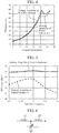
- FIG. 4 is an explanatory graph illustrating the power efficiency with respect to the output power of the Doherty amplifier of the first embodiment and the power efficiency with respect to the output power of the Doherty amplifier disclosed in Patent Literature 1.
- both Doherty amplifiers have high power efficiencies close to 80 (%).
- FIG. 5 is an explanatory graph illustrating simulation results of the frequency characteristics of power efficiency in back-off operation in the Doherty amplifier of the first embodiment and the frequency characteristics of power efficiency in back-off operation in the Doherty amplifier disclosed in Patent Literature 1.
- the horizontal axis represents the normalized frequency
- the vertical axis represents the power efficiency during the back-off operation.
- a first transmission line is connected to the output side of a carrier amplifier, and a second transmission line is connected to the output side of a peak amplifier, and thus the output impedance of the carrier amplifier and the output impedance of the peak amplifier are matched.
- a mismatch occurs between the output impedance of the carrier amplifier and the output impedance of the peak amplifier.
- the signal distributor 2 adjusts the phase shift amount of a signal by the phase shifter 7 depending on the frequency f of the digital signal D, and thus the power efficiency stays high as compared with the Doherty amplifier disclosed in Patent Literature 1 even when the fractional bandwidth of the frequency increases.
- the signal distributor 2 in a case where a power of a signal to be amplified is greater than or equal to a threshold value, the signal distributor 2 outputs one of signals to the carrier amplifier 6, outputs the other signal, the phase of which is 90 degrees behind that of the one of the signals, to the peak amplifier 8, and adjusts a phase shift amount of a signal by the phase shifter 7 depending on a frequency of the signal to be amplified, and in a case where the power of the signal to be amplified is less than the threshold value, the signal distributor 2 outputs the one of the signals to the carrier amplifier 6 without outputting the other signal to the peak amplifier 8.
- the signal distributor 2 outputs the one of the signals to the carrier amplifier 6 without outputting the other signal to the peak amplifier 8.
- the first embodiment illustrates the example in which the carrier amplifier 6 is implemented by an amplification element operating in class AB, and the peak amplifier 8 is implemented by an amplification element operating in class A or C.
- any semiconductor element having an amplification function can be used.
- a silicon (Si)-lateral double diffused MOS (LDMOS), a FET, a high electron mobility transistor (HEMT), or a hetero junction bipolar transistor (HBT) can be used.
- each of the carrier amplifier 6 and the peak amplifier 8 may include a parasitic component and a matching circuit.
- phase shifter 7 includes the inductive element 11, the first variable capacitance element 12, and the second variable capacitance element 13 is illustrated.
- phase shifter 7 includes a first inductive element 21, a second inductive element 22, and a variable capacitance element 23 will be described.
- FIG. 6 is a configuration diagram illustrating the phase shifter 7 of a Doherty amplifier according to the second embodiment of the present invention.
- the first inductive element 21 is an inductor one end of which is connected to the output side of the carrier amplifier 6.
- the second inductive element 22 is an inductor one end of which is connected to the other end of the first inductive element 21 and the other end of which is connected to one of the input sides of the signal synthesizer 9.
- variable capacitance element 23 is a variable capacitor one end of which is connected to the other end of the first inductive element 21 and the other end of which is grounded.
- a signal distributor 2 adjusts the phase shift amount in the phase shifter 7 depending on a frequency f of a digital signal D so that the phase delays by 90° by the phase shifter 7.
- phase shifter 7 a method for adjusting the phase shift amount by the phase shifter 7 will be specifically described.
- the signal distributor 2 stores a table indicating the relationship between the frequency f of the digital signal D and a capacitance value C of the variable capacitance element 23 in the phase shifter 7.
- the signal distributor 2 refers to the table to obtain the capacitance value C corresponding to the frequency f of the digital signal D.
- the signal distributor 2 adjusts the variable capacitance element 23 so that the capacitance value of the variable capacitance element 23 becomes the acquired value C.
- the signal distributor 2 adjusts the variable capacitance element 23 so that the capacitance value C of the variable capacitance element 23 becomes smaller than a reference capacitance value C 0 if the frequency f of the digital signal D is higher than a reference frequency f 0 .
- the signal distributor 2 adjusts the variable capacitance element 23 so that the capacitance value C of the variable capacitance element 23 becomes larger than the reference capacitance value C 0 if the frequency f of the digital signal D is lower than a reference frequency f 0 .
- the signal distributor 2 does not adjust the variable capacitance element 23 in a case where the frequency f of the digital signal D matches the reference frequency fo.
- phase shifter 7 includes the first inductive element 21, the second inductive element 22, and the variable capacitance element 23, the phase shift amount of a signal can be adjusted depending on the frequency f of the digital signal D like in the first embodiment.
- phase shifter 7 includes the inductive element 11, the first variable capacitance element 12, and the second variable capacitance element 13 is illustrated.
- phase shifter 7 includes a transmission line 31, a first variable capacitance element 32, and a second variable capacitance element 33 will be described.
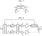
- FIG. 7 is a configuration diagram illustrating the phase shifter 7 of a Doherty amplifier according to a third embodiment of the present invention.
- the transmission line 31 is a line one end of which is connected to an output side of a carrier amplifier 6 and the other end of which is connected to one of the input sides of a signal synthesizer 9.
- the first variable capacitance element 32 is a variable capacitor one end of which is connected to the output side of the carrier amplifier 6 and the other end of which is grounded.
- the second variable capacitance element 33 is a variable capacitor one end of which is connected to one of the input sides of the signal synthesizer 9 and the other end of which is grounded.
- the signal distributor 2 adjusts the phase shift amount in the phase shifter 7 depending on a frequency f of a digital signal D so that the phase delays by 90° by the phase shifter 7.
- phase shifter 7 a method for adjusting the phase shift amount by the phase shifter 7 will be specifically described.
- the signal distributor 2 stores a table indicating the relationship between a frequency f of a digital signal D, a capacitance value C 1 of the first variable capacitance element 32 in the phase shifter 7 and a capacitance value C 2 of the second variable capacitance element 33 in the phase shifter 7.
- the signal distributor 2 refers to the table to obtain the capacitance value C 1 and the capacitance value C 2 each corresponding to the frequency f of the digital signal D.
- the signal distributor 2 adjusts the first variable capacitance element 32 so that the capacitance value of the first variable capacitance element 32 becomes the acquired value C 1 .
- the signal distributor 2 adjusts the second variable capacitance element 33 so that the capacitance value of the second variable capacitance element 33 becomes the acquired value C 2 .
- the signal distributor 2 adjusts the first variable capacitance element 32 so that the capacitance value C 1 of the first variable capacitance element 32 becomes smaller than a reference capacitance value C 1,0 if the frequency f of the digital signal D is higher than a reference frequency fo. Further, the signal distributor 2 adjusts the second variable capacitance element 33 so that the capacitance value C 2 of the second variable capacitance element 33 becomes smaller than a reference capacitance value C 2,0 .
- the signal distributor 2 adjusts the first variable capacitance element 32 so that the capacitance value C 1 of the first variable capacitance element 32 becomes larger than the reference capacitance value C 1,0 if the frequency f of the digital signal D is lower than the reference frequency fo. Further, the signal distributor 2 adjusts the second variable capacitance element 33 so that the capacitance value C 2 of the second variable capacitance element 33 becomes larger than the reference capacitance value C 2,0 .
- the signal distributor 2 does not adjust the first variable capacitance element 32 nor the second variable capacitance element 33 if the frequency f of the digital signal D matches the reference frequency f 0 .
- phase shifter 7 includes the transmission line 31, the first variable capacitance element 32, and the second variable capacitance element 33, the phase shift amount of a signal can be adjusted depending on the frequency f of the digital signal D like in the first embodiment.
- the Doherty amplifier including the carrier amplifier 6 and the peak amplifier 8 is illustrated.
- FIG. 8 is a configuration diagram illustrating a Doherty amplifier according to the fourth embodiment of the invention.
- the same symbols as those in FIG. 1 represent the same or corresponding parts and thus descriptions thereof are omitted.
- the first drive amplifier 41 amplifies a first analog signal A 1 output from an up-converter 5 and outputs the amplified first analog signal A 1 to the carrier amplifier 6.
- the second drive amplifier 42 amplifies a second analog signal A 2 output from the up-converter 5 and outputs the amplified second analog signal A 2 to the peak amplifier 8.
- the configuration of this embodiment is the same as the configuration of the first embodiment except that the first drive amplifier 41 is provided to the preceding stage of the carrier amplifier 6 and the second drive amplifier 42 is provided to the preceding stage of the peak amplifier 8.
- the output power of the Doherty amplifier can be enhanced more than that of the first embodiment.
- FIG. 9 is a configuration diagram illustrating an amplification circuit according to the fifth embodiment of the present invention.
- the same symbols as those in FIG. 1 represent the same or corresponding parts and thus descriptions thereof are omitted.
- a signal synthesizer 50 combines synthesized signals S output from two signal synthesizers 9, and outputs a synthesized signal of the two synthesized signals S to an output terminal 10.
- FIG. 9 the amplification circuit in which two Doherty amplifiers are connected in parallel is illustrated. Further, three or more Doherty amplifiers may be connected in parallel in an amplification circuit.
- the present invention may include a flexible combination of the respective embodiments, a modification of any component of the respective embodiments, or an omission of any component in the respective embodiments.
- the present invention is suitable for a Doherty amplifier and an amplification circuit for amplifying a signal to be amplified.
Landscapes
- Engineering & Computer Science (AREA)
- Power Engineering (AREA)
- Amplifiers (AREA)
Abstract
Description
- The present invention relates to a Doherty amplifier and an amplification circuit for amplifying a signal to be amplified.
- In amplification elements such as field effect transistors (FETs), high power efficiency is achieved, but the linearity of input/output characteristics is deteriorated at the time of large signal operation in which the operation is carried out near a saturation region.
- On the other hand, amplification elements have a disadvantage that the power efficiency is deteriorated while the linearity of input/output characteristics is improved at the time of small signal operation in which the operation is carried out in a power region lower than the saturation region. As amplifiers that solve these disadvantage, Doherty amplifiers are known.
- A Doherty amplifier disclosed in
Patent Literature 1 listed below includes the following components (1) to (7): - (1) A distributor for dividing a signal to be amplified into two signals;
- (2) A carrier amplifier for amplifying one of the signals distributed by the distributor;
- (3) A first transmission line, one end of which being connected to an output side of the carrier amplifier;
- (4) A phase shifter for delaying the phase of the other signal distributed by the distributor by 90 degrees;
- (5) A peak amplifier for amplifying the signal the phase of which being delayed by the phase shifter;
- (6) A second transmission line, one end of which being connected to an output side of the peak amplifier; and
- (7) A synthesizer, a first input terminal of which being connected to the other end of the first transmission line, and a second input terminal of which being connected to the other end of the second transmission line.
- Patent Literature 1:
JP 2006-332829 A - Doherty amplifiers are capable of implementing high linearity of input/output characteristics and high power efficiency by causing both a carrier amplifier and a peak amplifier to operate in a saturation region of the carrier amplifier and causing only the carrier amplifier to operate in a power region lower than the saturation region (hereinafter referred to as back-off operation).
- However, in the Doherty amplifier disclosed in
Patent Literature 1, a signal distributed by the distributor is always provided to the peak amplifier regardless of the power of the signal to be amplified. Therefore, there is a disadvantage that unnecessary power consumption occurs at the time of back-off operation since the peak amplifier operates even in the back-off operation. - Further, the first transmission line is connected to the output side of the carrier amplifier, and the second transmission line is connected to the output side of the peak amplifier, and thus the output impedance of the carrier amplifier and the output impedance of the peak amplifier are matched. However, when the frequency of a signal to be amplified changes from a desired frequency, a mismatch occurs between the output impedance of the carrier amplifier and the output impedance of the peak amplifier. Therefore, there is a disadvantage that the power efficiency is deteriorated when the frequency of a signal to be amplified changes from a desired frequency.
- The present invention has been made to solve the above-described disadvantages, and it is an object of the present invention to provide a Doherty amplifier and an amplification circuit capable of suppressing unnecessary power consumption at the time of back-off operation and suppressing deterioration of power efficiency even when a frequency of a signal to be amplified changes.
- A Doherty amplifier according to the present invention includes: a signal distributor dividing a signal to be amplified to signals and distributing the signals; a carrier amplifier amplifying one of the signals distributed by the signal distributor; a phase shifter adjusting a phase of the one of the signals amplified by the carrier amplifier; a peak amplifier amplifying another one of the signals distributed by the signal distributor; and a signal synthesizer synthesizing the one of the signals, the phase of which is adjusted by the phase shifter, and said another one of the signals amplified by the peak amplifier. In a case where a power of the signal to be amplified is greater than or equal to a threshold value, the signal distributor outputs the one of the signals to the carrier amplifier, outputs said another one of the signals, a phase of which is 90 degrees behind the phase of the one of the signals, to the peak amplifier, and adjusts a phase shift amount of a signal shifted by the phase shifter depending on a frequency of the signal to be amplified. In a case where the power of the signal to be amplified is less than the threshold value, the signal distributor outputs the one of the signals to the carrier amplifier without outputting another one of the signals to the peak amplifier.
- According to the present invention, in a case where a power of the signal to be amplified is greater than or equal to a threshold value, the signal distributor outputs the one of the signals to the carrier amplifier, outputs said another one of the signals, a phase of which is 90 degrees behind the phase of the one of the signals, to the peak amplifier, and adjusts a phase shift amount of a signal shifted by the phase shifter depending on a frequency of the signal to be amplified. In a case where the power of the signal to be amplified is less than the threshold value, the signal distributor outputs the one of the signals to the carrier amplifier without outputting another one of the signals to the peak amplifier. Therefore, there are effects of suppressing unnecessary power consumption at the time of back-off operation and suppressing deterioration of power efficiency even when a frequency of a signal to be amplified changes.
-
-
FIG. 1 is a configuration diagram illustrating a Doherty amplifier according to a first embodiment of the present invention. -
FIG. 2 is a configuration diagram illustrating aphase shifter 7 of the Doherty amplifier according to the first embodiment of the present invention. -
FIG. 3 is an explanatory graph illustrating the relationship of power between a first analog signal A1 which is an input signal of acarrier amplifier 6 and a second analog signal A2 which is an input signal of apeak amplifier 8. -
FIG. 4 is an explanatory graph illustrating the power efficiency with respect to the output power of the Doherty amplifier of the first embodiment and the power efficiency with respect to the output power of a Doherty amplifier disclosed inPatent Literature 1. -
FIG. 5 is an explanatory graph illustrating simulation results of the frequency characteristics of power efficiency in back-off operation in the Doherty amplifier of the first embodiment and the frequency characteristics of power efficiency in back-off operation in the Doherty amplifier disclosed inPatent Literature 1. -
FIG. 6 is a configuration diagram illustrating aphase shifter 7 of a Doherty amplifier according to a second embodiment of the present invention. -
FIG. 7 is a configuration diagram illustrating aphase shifter 7 of a Doherty amplifier according to a third embodiment of the present invention. -
FIG. 8 is a configuration diagram illustrating a Doherty amplifier according to a fourth embodiment of the present invention. -
FIG. 9 is a configuration diagram illustrating an amplification circuit according to a fifth embodiment of the present invention. - To describe the present invention further in detail, some embodiments for carrying out the present invention will be described below with reference to the accompanying drawings.
-
FIG. 1 is a configuration diagram illustrating a Doherty amplifier according to a first embodiment of the invention. - In
FIG. 1 , aninput terminal 1 receives input of a signal to be amplified. - In the first embodiment, an example in which a signal to be amplified is a digital signal will be described; however in a case where a signal to be amplified is an analog signal, digital/
analog converters - In
FIG. 1 , the digital/analog converters - A
signal distributor 2 distributes a digital signal D input from theinput terminal 1 and is implemented by, for example, a digital signal processor (DSP). - Specifically, the
signal distributor 2 compares a power P of the digital signal D input from theinput terminal 1 with a threshold value Pth set in advance. - The
signal distributor 2 outputs a first digital signal D1 which is one of the distributed digital signals to the digital/analog converter 3 and outputs a second digital signal D2 which is the other distributed digital signal to the digital/analog converter 4 in a case where the power P of the digital signal D input from theinput terminal 1 is greater than or equal to the threshold value Pth. At this time, thesignal distributor 2 sets the phase of the first digital signal D1 to θ1 = 0° and the phase of the second digital signal D2 to θ2 = -90°. - Furthermore, the
signal distributor 2 adjusts the phase shift amount of a signal in aphase shifter 7 depending on a frequency f of the digital signal D so that the phase delays by 90° by thephase shifter 7. - In a case where the power P of the digital signal D input from the
input terminal 1 is less than the threshold value Pth, thesignal distributor 2 outputs the first digital signal D1 to the digital/analog converter 3 without outputting the second digital signal D2 to the digital/analog converter 4. - The digital/
analog converter 3 converts the first digital signal D1 output from thesignal distributor 2 to the first analog signal A1 and outputs the first analog signal A1 to an up-converter 5. - The digital/
analog converter 4 converts the second digital signal D2 output from thesignal distributor 2 into a second analog signal A2 and outputs the second analog signal A2 to the up-converter 5. - The up-
converter 5 performs frequency conversion to increase the frequency of the first analog signal A1 output from the digital/analog converter 3, and outputs the first analog signal A1 after the frequency conversion to acarrier amplifier 6. - The up-
converter 5 performs frequency conversion to increase the frequency of the second analog signal A2 output from the digital/analog converter 4, and outputs the second analog signal A2 after the frequency conversion to apeak amplifier 8. - The
carrier amplifier 6 is implemented by, for example, an amplification element operating in class AB. - The
carrier amplifier 6 amplifies the first analog signal A1 output from the up-converter 5 and outputs the amplified first analog signal A1 to thephase shifter 7. - The
phase shifter 7 adjusts the phase of the amplified first analog signal A1 output from thecarrier amplifier 6 and outputs the phase-adjusted first analog signal A1 to asignal synthesizer 9. - The
peak amplifier 8 is implemented by, for example, an amplification element operating in class A or C. - The
peak amplifier 8 amplifies the second analog signal A2 output from the up-converter 5 and outputs the amplified second analog signal A2 to thesignal synthesizer 9. - The
signal synthesizer 9 is connected to an output side of thephase shifter 7 at one of input sides thereof and is connected to an output side of thepeak amplifier 8 at the other input side thereof. - The
signal synthesizer 9 synthesizes the phase-adjusted first analog signal A1 output from thephase shifter 7 and the amplified second analog signal A2 output from thepeak amplifier 8 and outputs a synthesized signal S of the first analog signal A1 and the second analog signal A2 to anoutput terminal 10. - The synthesized signal S is output from the
output terminal 10. -
FIG. 2 is a configuration diagram illustrating aphase shifter 7 of the Doherty amplifier according to a first embodiment of the present invention. - In
FIG. 2 , aninductive element 11 is an inductor having one end connected to an output side of thecarrier amplifier 6 and the other end connected to one input side of thesignal synthesizer 9. - A first
variable capacitance element 12 is a variable capacitor having one end connected to the output side of thecarrier amplifier 6 and the other end grounded, and having a capacitance value C1 adjusted by thesignal distributor 2. - A second
variable capacitance element 13 is a variable capacitor having one end connected to one input side of thesignal synthesizer 9 and the other end grounded, and having a capacitance value C2 adjusted by thesignal distributor 2. - Next, an operation will be described.
- When a digital signal D is input from the
input terminal 1, thesignal distributor 2 divides the digital signal D into two signals. - In this example, for convenience of explanation, one of the distributed digital signals is referred to as a first digital signal D1, and the other distributed digital signal is referred to as a second digital signal D2.
- The
signal distributor 2 compares a power P of the digital signal D with a threshold value Pth set in advance. - The threshold value Pth is set to a power such as a power at which the
carrier amplifier 6 saturates or a power several percent smaller than the power at which thecarrier amplifier 6 saturates. - In a case where the power P of the digital signal D is greater than or equal to the threshold value Pth, the
signal distributor 2 outputs the first digital signal D1 to the digital/analog converter 3 and outputs the second digital signal D2 to the digital/analog converter 4. - At this time, the
signal distributor 2 sets the phase of the first digital signal D1 to θ1 = 0° and the phase of the second digital signal D2 to θ2 = -90°. - In this example, the phase of the first digital signal D1 is set to θ1 = 0°, and the phase of the second digital signal D2 is set to θ2 = -90°; however, it is only required that the relation θ1 - θ2 = 90° holds, and thus, for example, they may be set such that θ1 = 20° and θ2 = -110°.
- Furthermore, the
signal distributor 2 adjusts the phase shift amount of a signal in thephase shifter 7 depending on a frequency f of the digital signal D so that the phase delays by 90° by thephase shifter 7. - Hereinafter, a method for adjusting the phase shift amount by the
phase shifter 7 will be specifically described. - The
signal distributor 2 stores a table indicating the relationship between the frequency f of the digital signal D, the capacitance value C1 of the firstvariable capacitance element 12 in thephase shifter 7 and the capacitance value C2 of the secondvariable capacitance element 13 in thephase shifter 7. - The
signal distributor 2 refers to the table to obtain the capacitance value C1 and the capacitance value C2 each corresponding to the frequency f of the digital signal D. - The
signal distributor 2 adjusts the firstvariable capacitance element 12 so that the capacitance value of the firstvariable capacitance element 12 becomes the acquired value C1. - The
signal distributor 2 adjusts the secondvariable capacitance element 13 so that the capacitance value of the secondvariable capacitance element 13 becomes the acquired value C2. - For example, if the frequency f of the digital signal D is higher than a reference frequency fo, the
signal distributor 2 adjusts the firstvariable capacitance element 12 so that the capacitance value C1 of the firstvariable capacitance element 12 becomes smaller than a reference capacitance value C1,0. Further, thesignal distributor 2 adjusts the secondvariable capacitance element 13 so that the capacitance value C2 of the secondvariable capacitance element 13 becomes smaller than a reference capacitance value C2,0. - If the frequency f of the digital signal D is lower than a reference frequency f0, the
signal distributor 2 adjusts the firstvariable capacitance element 12 so that the capacitance value C1 of the firstvariable capacitance element 12 becomes larger than the reference capacitance value C1,0. Further, thesignal distributor 2 adjusts the secondvariable capacitance element 13 so that the capacitance value C2 of the secondvariable capacitance element 13 becomes larger than the reference capacitance value C2,0. - If the frequency f of the digital signal D matches the reference frequency f0, the
signal distributor 2 does not adjust the firstvariable capacitance element 12 nor the secondvariable capacitance element 13. - As a result, even if the frequency f of the digital signal D changes, it is possible to set the phase shift amount of the signal by the
phase shifter 7 to 90°. Therefore, if the phase of the first digital signal D1 is set to θ1 = 0°, the phase of the output signal of thephase shifter 7 becomes -90°. - In a case where the power P of the digital signal D input from the
input terminal 1 is less than the threshold value Pth, thesignal distributor 2 outputs the first digital signal D1 to the digital/analog converter 3 without outputting the second digital signal D2 to the digital/analog converter 4. - Furthermore, the
signal distributor 2 adjusts the phase shift amount of a signal by thephase shifter 7 depending on the frequency f of the digital signal D so that the phase is delayed by 90° by thephase shifter 7 as in the case where the power P of the digital signal D is greater than or equal to the threshold value Pth. - Here, the
signal distributor 2 adjusts the phase shift amount of a signal by thephase shifter 7 also in a case where the power P of the digital signal D is less than the threshold value Pth. However, since the second digital signal D2 is not output to the digital/analog converter 4, thesignal synthesizer 9 outputs the first analog signal A1 as a synthesized signal S without synthesizing the first analog signal A1 and the second analog signal A2. Therefore, thesignal distributor 2 may be configured not to adjust the phase shift amount of a signal by thephase shifter 7. - The digital/
analog converter 3 converts the first digital signal D1 output from thesignal distributor 2 to the first analog signal A1 and outputs the first analog signal A1 to an up-converter 5. - In a case where the second digital signal D2 is output from the
signal distributor 2, the digital/analog converter 4 converts the second digital signal D2 into a second analog signal A2 and outputs the second analog signal A2 to the up-converter 5. - The up-
converter 5 performs frequency conversion to increase the frequency of the first analog signal A1 output from the digital/analog converter 3, and outputs the first analog signal A1 after the frequency conversion to acarrier amplifier 6. - In a case where the second analog signal A2 is output from the digital/
analog converter 4, the up-converter 5 performs frequency conversion to increase the frequency of the second analog signal A2, and outputs the second analog signal A2 after the frequency conversion to thepeak amplifier 8. - The
carrier amplifier 6 amplifies the first analog signal A1 output from the up-converter 5 and outputs the amplified first analog signal A1 to thephase shifter 7. - Since the first analog signal A1 is output from the up-
converter 5 regardless of whether the power P of the digital signal D is greater than or equal to the threshold value Pth, thecarrier amplifier 6 always amplifies the first analog signal A1. - The
peak amplifier 8 amplifies the second analog signal A2 output from the up-converter 5 and outputs the amplified second analog signal A2 to thesignal synthesizer 9. - The second analog signal A2 is output from the up-
converter 5 only in the case where the power P of the digital signal D is greater than or equal to the threshold value Pth. Therefore, thepeak amplifier 8 amplifies the second analog signal A2 in the saturation region of thecarrier amplifier 6, but does not amplify the second analog signal A2 in a power region lower than the saturation region of thecarrier amplifier 6. - Therefore, back-off operation in which only the
carrier amplifier 6 operates is performed in a power region lower than the saturation region. - The
phase shifter 7 adjusts the phase of the amplified first analog signal A1 output from thecarrier amplifier 6 and outputs the phase-adjusted first analog signal A1 to asignal synthesizer 9. - Since the phase shift amount of a signal by the
phase shifter 7 is adjusted by thesignal distributor 2 depending on the frequency f of the digital signal D, even when the frequency f of the digital signal D changes, the phase of the first analog signal A1 after the phase adjustment by thephase shifter 7 becomes -90°. - In the saturation region of the
carrier amplifier 6, thesignal synthesizer 9 synthesizes the phase-adjusted first analog signal A1 output from thephase shifter 7 and the amplified second analog signal A2 output from thepeak amplifier 8 and outputs a synthesized signal S of the first analog signal A1 and the second analog signal A2 to theoutput terminal 10. - The phase of the phase-adjusted first analog signal A1 output from the
phase shifter 7 is -90°, and the phase of the amplified second analog signal A2 output from thepeak amplifier 8 is -90°, and thus in thesignal synthesizer 9, the first analog signal A1 and the second analog signal A2 are in-phase synthesized. - In a power region lower than the saturation region, the back-off operation, in which only the
carrier amplifier 6 operates, is performed, and the amplified second analog signal A2 is not output from thepeak amplifier 8. Therefore, thesignal synthesizer 9 outputs the phase-adjusted first analog signal A1 output from thephase shifter 7 to theoutput terminal 10 as a synthesized signal S. - In the back-off operation, since the second analog signal A2 is not input to the
peak amplifier 8, unnecessary power consumption in thepeak amplifier 8 can be suppressed. -
FIG. 3 is an explanatory graph illustrating the relationship of power between the first analog signal A1 which is an input signal of thecarrier amplifier 6 and the second analog signal A2 which is an input signal of thepeak amplifier 8. - In the example of
FIG. 3 , -6 to 0 (dBm) is the saturation region of thecarrier amplifier 6. - In the example of
FIG. 3 , it is illustrated that the first analog signal A1 is linearly input to thecarrier amplifier 6, whereas the second analog signal A2 is input to thepeak amplifier 8 only when thecarrier amplifier 6 is in the saturation region. - In the example of
FIG. 3 , the threshold value Pth in thesignal distributor 2 is set to -6 (dBm), for example. -
FIG. 4 is an explanatory graph illustrating the power efficiency with respect to the output power of the Doherty amplifier of the first embodiment and the power efficiency with respect to the output power of the Doherty amplifier disclosed inPatent Literature 1. - It can be seen from
FIG. 4 that, in both Doherty amplifiers, thecarrier amplifiers 6 and thepeak amplifiers 8 operate in parallel in the saturation region of thecarrier amplifier 6, thereby improving the power efficiency. - For example, when the output power in the saturation region of the
carrier amplifier 6 is 27 (dBm), both Doherty amplifiers have high power efficiencies close to 80 (%). - In the Doherty amplifier disclosed in
Patent Literature 1, a signal to be amplified is provided to the peak amplifier even in the back-off operation. This causes the peak amplifier to operate, and thus the power efficiency is lower than that of the Doherty amplifier of the first embodiment. -
FIG. 5 is an explanatory graph illustrating simulation results of the frequency characteristics of power efficiency in back-off operation in the Doherty amplifier of the first embodiment and the frequency characteristics of power efficiency in back-off operation in the Doherty amplifier disclosed inPatent Literature 1. - In
FIG. 5 , the horizontal axis represents the normalized frequency, and the vertical axis represents the power efficiency during the back-off operation. - In the Doherty amplifier disclosed in
Patent Literature 1, a first transmission line is connected to the output side of a carrier amplifier, and a second transmission line is connected to the output side of a peak amplifier, and thus the output impedance of the carrier amplifier and the output impedance of the peak amplifier are matched. However, when the frequency of a signal to be amplified changes from a desired frequency, a mismatch occurs between the output impedance of the carrier amplifier and the output impedance of the peak amplifier. - For this reason, as illustrated in
FIG. 5 , the power efficiency of the Doherty amplifier disclosed inPatent Literature 1 decreases as the fractional bandwidth of the frequency increases. - In the Doherty amplifier according to the first embodiment, the
signal distributor 2 adjusts the phase shift amount of a signal by thephase shifter 7 depending on the frequency f of the digital signal D, and thus the power efficiency stays high as compared with the Doherty amplifier disclosed inPatent Literature 1 even when the fractional bandwidth of the frequency increases. - As apparent from the above, according to the first embodiment, in a case where a power of a signal to be amplified is greater than or equal to a threshold value, the
signal distributor 2 outputs one of signals to thecarrier amplifier 6, outputs the other signal, the phase of which is 90 degrees behind that of the one of the signals, to thepeak amplifier 8, and adjusts a phase shift amount of a signal by thephase shifter 7 depending on a frequency of the signal to be amplified, and in a case where the power of the signal to be amplified is less than the threshold value, thesignal distributor 2 outputs the one of the signals to thecarrier amplifier 6 without outputting the other signal to thepeak amplifier 8. As a result, it is possible to suppress unnecessary power consumption at the time of back-off operation and to suppress deterioration of power efficiency even when a frequency of a signal to be amplified changes. - The first embodiment illustrates the example in which the
carrier amplifier 6 is implemented by an amplification element operating in class AB, and thepeak amplifier 8 is implemented by an amplification element operating in class A or C. - For the amplification element to implement the
carrier amplifier 6 or thepeak amplifier 8, any semiconductor element having an amplification function can be used. For example, a silicon (Si)-lateral double diffused MOS (LDMOS), a FET, a high electron mobility transistor (HEMT), or a hetero junction bipolar transistor (HBT) can be used. - Further, each of the
carrier amplifier 6 and thepeak amplifier 8 may include a parasitic component and a matching circuit. - In the first embodiment, an example in which the
phase shifter 7 includes theinductive element 11, the firstvariable capacitance element 12, and the secondvariable capacitance element 13 is illustrated. - In a second embodiment, an example in which a
phase shifter 7 includes a firstinductive element 21, a secondinductive element 22, and a variable capacitance element 23 will be described. -
FIG. 6 is a configuration diagram illustrating thephase shifter 7 of a Doherty amplifier according to the second embodiment of the present invention. - In
FIG. 6 , the firstinductive element 21 is an inductor one end of which is connected to the output side of thecarrier amplifier 6. - The second
inductive element 22 is an inductor one end of which is connected to the other end of the firstinductive element 21 and the other end of which is connected to one of the input sides of thesignal synthesizer 9. - The variable capacitance element 23 is a variable capacitor one end of which is connected to the other end of the first
inductive element 21 and the other end of which is grounded. - Next, the operation will be described.
- A
signal distributor 2 adjusts the phase shift amount in thephase shifter 7 depending on a frequency f of a digital signal D so that the phase delays by 90° by thephase shifter 7. - Hereinafter, a method for adjusting the phase shift amount by the
phase shifter 7 will be specifically described. - The
signal distributor 2 stores a table indicating the relationship between the frequency f of the digital signal D and a capacitance value C of the variable capacitance element 23 in thephase shifter 7. - The
signal distributor 2 refers to the table to obtain the capacitance value C corresponding to the frequency f of the digital signal D. - The
signal distributor 2 adjusts the variable capacitance element 23 so that the capacitance value of the variable capacitance element 23 becomes the acquired value C. - For example, the
signal distributor 2 adjusts the variable capacitance element 23 so that the capacitance value C of the variable capacitance element 23 becomes smaller than a reference capacitance value C0 if the frequency f of the digital signal D is higher than a reference frequency f0. - The
signal distributor 2 adjusts the variable capacitance element 23 so that the capacitance value C of the variable capacitance element 23 becomes larger than the reference capacitance value C0 if the frequency f of the digital signal D is lower than a reference frequency f0. - The
signal distributor 2 does not adjust the variable capacitance element 23 in a case where the frequency f of the digital signal D matches the reference frequency fo. - As a result, even if the frequency f of the digital signal D changes, it is possible to set the phase shift amount of the signal by the
phase shifter 7 to 90°. Therefore, if the phase of the first digital signal D1 is set to θ1 = 0°, the phase of the output signal of thephase shifter 7 becomes -90°. - Also in a case where the
phase shifter 7 includes the firstinductive element 21, the secondinductive element 22, and the variable capacitance element 23, the phase shift amount of a signal can be adjusted depending on the frequency f of the digital signal D like in the first embodiment. - In the first embodiment, an example in which the
phase shifter 7 includes theinductive element 11, the firstvariable capacitance element 12, and the secondvariable capacitance element 13 is illustrated. - In a second embodiment, an example in which a
phase shifter 7 includes atransmission line 31, a firstvariable capacitance element 32, and a secondvariable capacitance element 33 will be described. -
FIG. 7 is a configuration diagram illustrating thephase shifter 7 of a Doherty amplifier according to a third embodiment of the present invention. - In
FIG. 7 , thetransmission line 31 is a line one end of which is connected to an output side of acarrier amplifier 6 and the other end of which is connected to one of the input sides of asignal synthesizer 9. - The first
variable capacitance element 32 is a variable capacitor one end of which is connected to the output side of thecarrier amplifier 6 and the other end of which is grounded. - The second
variable capacitance element 33 is a variable capacitor one end of which is connected to one of the input sides of thesignal synthesizer 9 and the other end of which is grounded. - The
signal distributor 2 adjusts the phase shift amount in thephase shifter 7 depending on a frequency f of a digital signal D so that the phase delays by 90° by thephase shifter 7. - Hereinafter, a method for adjusting the phase shift amount by the
phase shifter 7 will be specifically described. - The
signal distributor 2 stores a table indicating the relationship between a frequency f of a digital signal D, a capacitance value C1 of the firstvariable capacitance element 32 in thephase shifter 7 and a capacitance value C2 of the secondvariable capacitance element 33 in thephase shifter 7. - The
signal distributor 2 refers to the table to obtain the capacitance value C1 and the capacitance value C2 each corresponding to the frequency f of the digital signal D. - The
signal distributor 2 adjusts the firstvariable capacitance element 32 so that the capacitance value of the firstvariable capacitance element 32 becomes the acquired value C1. - Further, the
signal distributor 2 adjusts the secondvariable capacitance element 33 so that the capacitance value of the secondvariable capacitance element 33 becomes the acquired value C2. - For example, the
signal distributor 2 adjusts the firstvariable capacitance element 32 so that the capacitance value C1 of the firstvariable capacitance element 32 becomes smaller than a reference capacitance value C1,0 if the frequency f of the digital signal D is higher than a reference frequency fo. Further, thesignal distributor 2 adjusts the secondvariable capacitance element 33 so that the capacitance value C2 of the secondvariable capacitance element 33 becomes smaller than a reference capacitance value C2,0. - The
signal distributor 2 adjusts the firstvariable capacitance element 32 so that the capacitance value C1 of the firstvariable capacitance element 32 becomes larger than the reference capacitance value C1,0 if the frequency f of the digital signal D is lower than the reference frequency fo. Further, thesignal distributor 2 adjusts the secondvariable capacitance element 33 so that the capacitance value C2 of the secondvariable capacitance element 33 becomes larger than the reference capacitance value C2,0. - The
signal distributor 2 does not adjust the firstvariable capacitance element 32 nor the secondvariable capacitance element 33 if the frequency f of the digital signal D matches the reference frequency f0. - As a result, even if the frequency f of the digital signal D changes, it is possible to set the phase shift amount of the signal by the
phase shifter 7 to 90°. Therefore, if the phase of the first digital signal D1 is set to θ1 = 0°, the phase of the output signal of thephase shifter 7 becomes -90°. - Also in a case where the
phase shifter 7 includes thetransmission line 31, the firstvariable capacitance element 32, and the secondvariable capacitance element 33, the phase shift amount of a signal can be adjusted depending on the frequency f of the digital signal D like in the first embodiment. - In the first embodiment, the Doherty amplifier including the
carrier amplifier 6 and thepeak amplifier 8 is illustrated. - In a fourth embodiment, an example in which a
first drive amplifier 41 is connected to acarrier amplifier 6 in series and asecond drive amplifier 42 is connected to apeak amplifier 8 in series will be described. -
FIG. 8 is a configuration diagram illustrating a Doherty amplifier according to the fourth embodiment of the invention. InFIG. 8 , the same symbols as those inFIG. 1 represent the same or corresponding parts and thus descriptions thereof are omitted. - The
first drive amplifier 41 amplifies a first analog signal A1 output from an up-converter 5 and outputs the amplified first analog signal A1 to thecarrier amplifier 6. - The
second drive amplifier 42 amplifies a second analog signal A2 output from the up-converter 5 and outputs the amplified second analog signal A2 to thepeak amplifier 8. - The configuration of this embodiment is the same as the configuration of the first embodiment except that the
first drive amplifier 41 is provided to the preceding stage of thecarrier amplifier 6 and thesecond drive amplifier 42 is provided to the preceding stage of thepeak amplifier 8. - By amplifying the first analog signal A1 by the
first drive amplifier 41, and by amplifying the second analog signal A2 by thesecond drive amplifier 42, the output power of the Doherty amplifier can be enhanced more than that of the first embodiment. - In a fifth embodiment, an amplification circuit in which multiple Doherty amplifiers are connected in parallel will be described.
-
FIG. 9 is a configuration diagram illustrating an amplification circuit according to the fifth embodiment of the present invention. InFIG. 9 , the same symbols as those inFIG. 1 represent the same or corresponding parts and thus descriptions thereof are omitted. - A
signal synthesizer 50 combines synthesized signals S output from twosignal synthesizers 9, and outputs a synthesized signal of the two synthesized signals S to anoutput terminal 10. - In
FIG. 9 , the amplification circuit in which two Doherty amplifiers are connected in parallel is illustrated. Further, three or more Doherty amplifiers may be connected in parallel in an amplification circuit. - Even in a case where multiple Doherty amplifiers are connected in parallel, it is possible to suppress unnecessary power consumption at the time of back-off operation and to suppress deterioration of power efficiency like in the first embodiment even when a frequency of a signal to be amplified changes.
- Note that, within the scope of the present invention, the present invention may include a flexible combination of the respective embodiments, a modification of any component of the respective embodiments, or an omission of any component in the respective embodiments.
- The present invention is suitable for a Doherty amplifier and an amplification circuit for amplifying a signal to be amplified.
- 1: Input terminal, 2: Signal distributor, 3, 4: Digital/analog converter, 5: Up-converter, 6: Carrier amplifier, 7: Phase shifter, 8: Peak amplifier, 9: Signal synthesizer, 10: Output terminal, 11: Inductive element, 12: First variable capacitance element, 13: Second variable capacitance element, 21: First inductive element, 22: Second inductive element, 23: Variable capacitance element, 31: Transmission line, 32: First variable capacitance element, 33: Second variable capacitance element, 41: First drive amplifier, 42: Second drive amplifier, 50: Signal synthesizer.
Claims (6)
- A Doherty amplifier comprising:a signal distributor dividing a signal to be amplified to signals and distributing the signals;a carrier amplifier amplifying one of the signals distributed by the signal distributor;a phase shifter adjusting a phase of the one of the signals amplified by the carrier amplifier;a peak amplifier amplifying another one of the signals distributed by the signal distributor; anda signal synthesizer synthesizing the one of the signals, the phase of which is adjusted by the phase shifter, and said another one of the signals amplified by the peak amplifier,wherein in a case where a power of the signal to be amplified is greater than or equal to a threshold value, the signal distributor outputs the one of the signals to the carrier amplifier, outputs said another one of the signals, a phase of which is 90 degrees behind the phase of the one of the signals, to the peak amplifier, and adjusts a phase shift amount of a signal shifted by the phase shifter depending on a frequency of the signal to be amplified, andin a case where the power of the signal to be amplified is less than the threshold value, the signal distributor outputs the one of the signals to the carrier amplifier without outputting said another one of the signals to the peak amplifier.
- The Doherty amplifier according to claim 1, wherein the phase shifter includes:an inductive element, one end of which is connected to an output side of the carrier amplifier and another end of which is connected to one of input sides of the signal synthesizer;a first variable capacitance element, one end of which is connected to the output side of the carrier amplifier and another end of which is grounded; anda second variable capacitance element, one end of which is connected to the one of the input sides of the signal synthesizer and another end of which is grounded.
- The Doherty amplifier according to claim 1, wherein the phase shifter includes:a first inductive element, one end of which is connected to an output side of the carrier amplifier;a second inductive element, one end of which is connected to another end of the first inductive element and another end of which is connected to one of input sides of the signal synthesizer; anda variable capacitance element, one end of which is connected to the other end of the first inductive element and another end of which is grounded.
- The Doherty amplifier according to claim 1, wherein the phase shifter includes:a transmission line, one end of which is connected to an output side of the carrier amplifier and another end of which is connected to one of input sides of the signal synthesizer;a first variable capacitance element, one end of which is connected to the output side of the carrier amplifier and another end of which is grounded; anda second variable capacitance element, one end of which is connected to the one of the input sides of the signal synthesizer and another end of which is grounded.
- The Doherty amplifier according to claim 1, further comprising:a first drive amplifier amplifying one of the signals distributed by the signal distributor and outputting the amplified signal to the carrier amplifier; anda second drive amplifier amplifying another one of the signals distributed by the signal distributor and outputting the amplified signal to the peak amplifier.
- An amplification circuit including a plurality of Doherty amplifiers connected to each other in parallel, wherein each of the plurality of Doherty amplifiers includes:a signal distributor dividing a signal to be amplified to signals and distributing the signals;a carrier amplifier amplifying one of the signals distributed by the signal distributor;a phase shifter adjusting a phase of the one of the signals amplified by the carrier amplifier;a peak amplifier amplifying another one of the signals distributed by the signal distributor; anda signal synthesizer synthesizing the one of the signals, the phase of which is adjusted by the phase shifter, and said another one of the signals amplified by the peak amplifier,wherein in a case where a power of the signal to be amplified is greater than or equal to a threshold value, the signal distributor outputs the one of the signals to the carrier amplifier, outputs said another one of the signals, a phase of which is 90 degrees behind the phase of the one of the signals, to the peak amplifier, and adjusts a phase shift amount of a signal shifted by the phase shifter depending on a frequency of the signal to be amplified, andin a case where the power of the signal to be amplified is less than the threshold value, the signal distributor outputs the one of the signals to the carrier amplifier without outputting said another one of the signals to the peak amplifier.
Applications Claiming Priority (1)
| Application Number | Priority Date | Filing Date | Title |
|---|---|---|---|
| PCT/JP2017/027277 WO2019021426A1 (en) | 2017-07-27 | 2017-07-27 | Doherty amplifier and amplification circuit |
Publications (3)
| Publication Number | Publication Date |
|---|---|
| EP3648343A1 true EP3648343A1 (en) | 2020-05-06 |
| EP3648343A4 EP3648343A4 (en) | 2020-07-08 |
| EP3648343B1 EP3648343B1 (en) | 2022-09-07 |
Family
ID=63855171
Family Applications (1)
| Application Number | Title | Priority Date | Filing Date |
|---|---|---|---|
| EP17919295.0A Active EP3648343B1 (en) | 2017-07-27 | 2017-07-27 | Doherty amplifier and amplification circuit |
Country Status (5)
| Country | Link |
|---|---|
| US (1) | US20200136564A1 (en) |
| EP (1) | EP3648343B1 (en) |
| JP (1) | JP6407476B1 (en) |
| CN (1) | CN110945782B (en) |
| WO (1) | WO2019021426A1 (en) |
Cited By (1)
| Publication number | Priority date | Publication date | Assignee | Title |
|---|---|---|---|---|
| EP4156508A4 (en) * | 2020-06-24 | 2023-07-19 | Mitsubishi Electric Corporation | Doherty amplifier |
Families Citing this family (7)
| Publication number | Priority date | Publication date | Assignee | Title |
|---|---|---|---|---|
| WO2020208813A1 (en) * | 2019-04-12 | 2020-10-15 | 三菱電機株式会社 | Doherty amplifier circuit |
| US11108361B2 (en) * | 2019-08-15 | 2021-08-31 | Nxp Usa, Inc. | Integrated multiple-path power amplifier with interdigitated transistors |
| JP7435193B2 (en) * | 2020-04-14 | 2024-02-21 | 住友電気工業株式会社 | high frequency amplifier |
| EP4123902B1 (en) * | 2020-04-27 | 2024-07-10 | Mitsubishi Electric Corporation | Doherty amplifier |
| CN116888887A (en) * | 2021-02-12 | 2023-10-13 | 株式会社村田制作所 | Power amplifying circuit |
| CN116094529B (en) * | 2023-01-03 | 2025-12-23 | 芯百特微电子(无锡)有限公司 | Radio frequency front end module for Wifi communication and communication terminal |
| WO2024157642A1 (en) * | 2023-01-27 | 2024-08-02 | 株式会社村田製作所 | Amplification circuit and communication device |
Family Cites Families (24)
| Publication number | Priority date | Publication date | Assignee | Title |
|---|---|---|---|---|
| JPS4972139U (en) * | 1972-10-05 | 1974-06-22 | ||
| CN100477494C (en) * | 2002-08-19 | 2009-04-08 | Nxp股份有限公司 | High power Doherty amplifier |
| JP2005117599A (en) * | 2003-10-08 | 2005-04-28 | Hiroshi Suzuki | High frequency amplifier |
| JP4715994B2 (en) * | 2004-08-26 | 2011-07-06 | 日本電気株式会社 | Doherty amplifier parallel operation circuit |
| JP2006166141A (en) * | 2004-12-08 | 2006-06-22 | Matsushita Electric Ind Co Ltd | Doherty amplifier |
| US7248108B2 (en) * | 2004-12-29 | 2007-07-24 | Agere Systems Inc. | Power amplifier employing thin film ferroelectric phase shift element |
| JP4793807B2 (en) | 2005-05-24 | 2011-10-12 | 株式会社日立国際電気 | amplifier |
| JP2006333022A (en) * | 2005-05-26 | 2006-12-07 | Matsushita Electric Ind Co Ltd | High frequency power amplifier |
| JP2007019578A (en) * | 2005-07-05 | 2007-01-25 | Hitachi Ltd | Power amplifier and transmitter using the same |
| JP2009539277A (en) * | 2006-04-26 | 2009-11-12 | エヌエックスピー ビー ヴィ | High power integrated RF amplifier |
| WO2008111172A1 (en) * | 2007-03-13 | 2008-09-18 | Panasonic Corporation | Power amplifier |
| US8335481B2 (en) * | 2007-12-05 | 2012-12-18 | Telefonaktiebolaget L M Ericsson (Publ) | Load modulation arrangement |
| JP5169274B2 (en) * | 2008-02-12 | 2013-03-27 | 住友電気工業株式会社 | Doherty amplifier |
| JP2009260472A (en) * | 2008-04-14 | 2009-11-05 | Mitsubishi Electric Corp | Power amplifier |
| JP5316295B2 (en) * | 2009-08-04 | 2013-10-16 | 富士通株式会社 | Doherty amplifier |
| US8749306B2 (en) * | 2011-03-16 | 2014-06-10 | Cree, Inc. | Enhanced Doherty amplifier |
| CN102427332B (en) * | 2011-11-28 | 2015-04-08 | 华为技术有限公司 | Doherty power amplifier and method and equipment for improving power amplification efficiency of Doherty power amplifier |
| EP2658116A1 (en) * | 2012-04-23 | 2013-10-30 | Alcatel-Lucent | Amplifier circuit |
| JP5747008B2 (en) * | 2012-09-21 | 2015-07-08 | 旭化成エレクトロニクス株式会社 | Doherty amplifier |
| US9225291B2 (en) * | 2013-10-29 | 2015-12-29 | Freescale Semiconductor, Inc. | Adaptive adjustment of power splitter |
| JP2015220680A (en) * | 2014-05-20 | 2015-12-07 | 三菱電機株式会社 | High efficiency amplifier |
| JP6218120B2 (en) * | 2014-07-10 | 2017-10-25 | 株式会社村田製作所 | Power amplifier |
| JP2016111638A (en) * | 2014-12-10 | 2016-06-20 | 三星電子株式会社Samsung Electronics Co.,Ltd. | Power amplifier |
| JP6606877B2 (en) * | 2015-06-09 | 2019-11-20 | 富士通株式会社 | Wireless communication device |
-
2017
- 2017-07-27 US US16/627,950 patent/US20200136564A1/en not_active Abandoned
- 2017-07-27 JP JP2018506354A patent/JP6407476B1/en active Active
- 2017-07-27 EP EP17919295.0A patent/EP3648343B1/en active Active
- 2017-07-27 WO PCT/JP2017/027277 patent/WO2019021426A1/en not_active Ceased
- 2017-07-27 CN CN201780093302.XA patent/CN110945782B/en active Active
Cited By (1)
| Publication number | Priority date | Publication date | Assignee | Title |
|---|---|---|---|---|
| EP4156508A4 (en) * | 2020-06-24 | 2023-07-19 | Mitsubishi Electric Corporation | Doherty amplifier |
Also Published As
| Publication number | Publication date |
|---|---|
| JPWO2019021426A1 (en) | 2019-07-25 |
| JP6407476B1 (en) | 2018-10-17 |
| CN110945782B (en) | 2024-03-01 |
| CN110945782A (en) | 2020-03-31 |
| EP3648343B1 (en) | 2022-09-07 |
| WO2019021426A1 (en) | 2019-01-31 |
| US20200136564A1 (en) | 2020-04-30 |
| EP3648343A4 (en) | 2020-07-08 |
Similar Documents
| Publication | Publication Date | Title |
|---|---|---|
| EP3648343A1 (en) | Doherty amplifier and amplification circuit | |
| US8180304B2 (en) | Efficient power amplifier | |
| US9030255B2 (en) | Linearization circuit and related techniques | |
| US8466746B2 (en) | Three-stage GaN HEMT doherty power amplifier for high frequency applications | |
| US7560984B2 (en) | Transmitter | |
| EP2451074B1 (en) | Amplifier | |
| US10911003B2 (en) | Doherty amplifier | |
| CN108111129B (en) | Power amplifier | |
| JP2004222151A (en) | Doherty amplifier | |
| Watkins et al. | How not to rely on Moore's Law alone: low-complexity envelope-tracking amplifiers | |
| EP2879291A1 (en) | Broadband RF power amplifier with active load modulation | |
| JP2014217058A (en) | Amplifier using nonlinear driver | |
| JP2008193720A (en) | Doherty amplifier circuit | |
| JP2014135726A (en) | Broadband high efficiency amplifier system | |
| JP2012199706A (en) | Doherty amplification device | |
| JP7281933B2 (en) | amplifier | |
| EP2642660A2 (en) | Linearization circuit and related techniques | |
| US20250023521A1 (en) | Doherty amplifier | |
| JP2008022513A (en) | Amplification device with distortion control function | |
| EP2475094A1 (en) | Doherty amplifier | |
| EP2472718B1 (en) | Method and system to amplify a digital signal | |
| JP7337270B2 (en) | doherty amplifier | |
| JP4825495B2 (en) | Amplification device with distortion control function | |
| CN113875150B (en) | Doherty amplifier and communication device | |
| US8294519B2 (en) | Power amplifying apparatus and power amplifying method |
Legal Events
| Date | Code | Title | Description |
|---|---|---|---|
| STAA | Information on the status of an ep patent application or granted ep patent |
Free format text: STATUS: THE INTERNATIONAL PUBLICATION HAS BEEN MADE |
|
| PUAI | Public reference made under article 153(3) epc to a published international application that has entered the european phase |
Free format text: ORIGINAL CODE: 0009012 |
|
| STAA | Information on the status of an ep patent application or granted ep patent |
Free format text: STATUS: REQUEST FOR EXAMINATION WAS MADE |
|
| 17P | Request for examination filed |
Effective date: 20200111 |
|
| AK | Designated contracting states |
Kind code of ref document: A1 Designated state(s): AL AT BE BG CH CY CZ DE DK EE ES FI FR GB GR HR HU IE IS IT LI LT LU LV MC MK MT NL NO PL PT RO RS SE SI SK SM TR |
|
| AX | Request for extension of the european patent |
Extension state: BA ME |
|
| A4 | Supplementary search report drawn up and despatched |
Effective date: 20200609 |
|
| RIC1 | Information provided on ipc code assigned before grant |
Ipc: H03F 1/02 20060101ALI20200604BHEP Ipc: H03F 3/60 20060101ALI20200604BHEP Ipc: H03F 3/21 20060101ALI20200604BHEP Ipc: H03F 1/07 20060101AFI20200604BHEP |
|
| DAV | Request for validation of the european patent (deleted) | ||
| DAX | Request for extension of the european patent (deleted) | ||
| STAA | Information on the status of an ep patent application or granted ep patent |
Free format text: STATUS: EXAMINATION IS IN PROGRESS |
|
| 17Q | First examination report despatched |
Effective date: 20201223 |
|
| REG | Reference to a national code |
Ref country code: DE Ref legal event code: R079 Ref document number: 602017061702 Country of ref document: DE Free format text: PREVIOUS MAIN CLASS: H03F0001070000 Ipc: H01P0001180000 |
|
| GRAP | Despatch of communication of intention to grant a patent |
Free format text: ORIGINAL CODE: EPIDOSNIGR1 |
|
| STAA | Information on the status of an ep patent application or granted ep patent |
Free format text: STATUS: GRANT OF PATENT IS INTENDED |
|
| RIC1 | Information provided on ipc code assigned before grant |
Ipc: H03F 3/60 20060101ALI20220318BHEP Ipc: H03F 3/21 20060101ALI20220318BHEP Ipc: H03F 1/02 20060101ALI20220318BHEP Ipc: H01P 1/18 20060101AFI20220318BHEP |
|
| INTG | Intention to grant announced |
Effective date: 20220412 |
|
| GRAS | Grant fee paid |
Free format text: ORIGINAL CODE: EPIDOSNIGR3 |
|
| GRAA | (expected) grant |
Free format text: ORIGINAL CODE: 0009210 |
|
| STAA | Information on the status of an ep patent application or granted ep patent |
Free format text: STATUS: THE PATENT HAS BEEN GRANTED |
|
| AK | Designated contracting states |
Kind code of ref document: B1 Designated state(s): AL AT BE BG CH CY CZ DE DK EE ES FI FR GB GR HR HU IE IS IT LI LT LU LV MC MK MT NL NO PL PT RO RS SE SI SK SM TR |
|
| REG | Reference to a national code |
Ref country code: GB Ref legal event code: FG4D |
|
| REG | Reference to a national code |
Ref country code: CH Ref legal event code: EP Ref country code: AT Ref legal event code: REF Ref document number: 1517817 Country of ref document: AT Kind code of ref document: T Effective date: 20220915 |
|
| REG | Reference to a national code |
Ref country code: DE Ref legal event code: R096 Ref document number: 602017061702 Country of ref document: DE |
|
| REG | Reference to a national code |
Ref country code: IE Ref legal event code: FG4D |
|
| REG | Reference to a national code |
Ref country code: LT Ref legal event code: MG9D |
|
| REG | Reference to a national code |
Ref country code: NL Ref legal event code: MP Effective date: 20220907 |
|
| PG25 | Lapsed in a contracting state [announced via postgrant information from national office to epo] |
Ref country code: SE Free format text: LAPSE BECAUSE OF FAILURE TO SUBMIT A TRANSLATION OF THE DESCRIPTION OR TO PAY THE FEE WITHIN THE PRESCRIBED TIME-LIMIT Effective date: 20220907 Ref country code: RS Free format text: LAPSE BECAUSE OF FAILURE TO SUBMIT A TRANSLATION OF THE DESCRIPTION OR TO PAY THE FEE WITHIN THE PRESCRIBED TIME-LIMIT Effective date: 20220907 Ref country code: NO Free format text: LAPSE BECAUSE OF FAILURE TO SUBMIT A TRANSLATION OF THE DESCRIPTION OR TO PAY THE FEE WITHIN THE PRESCRIBED TIME-LIMIT Effective date: 20221207 Ref country code: LV Free format text: LAPSE BECAUSE OF FAILURE TO SUBMIT A TRANSLATION OF THE DESCRIPTION OR TO PAY THE FEE WITHIN THE PRESCRIBED TIME-LIMIT Effective date: 20220907 Ref country code: LT Free format text: LAPSE BECAUSE OF FAILURE TO SUBMIT A TRANSLATION OF THE DESCRIPTION OR TO PAY THE FEE WITHIN THE PRESCRIBED TIME-LIMIT Effective date: 20220907 Ref country code: FI Free format text: LAPSE BECAUSE OF FAILURE TO SUBMIT A TRANSLATION OF THE DESCRIPTION OR TO PAY THE FEE WITHIN THE PRESCRIBED TIME-LIMIT Effective date: 20220907 |
|
| REG | Reference to a national code |
Ref country code: AT Ref legal event code: MK05 Ref document number: 1517817 Country of ref document: AT Kind code of ref document: T Effective date: 20220907 |
|
| PG25 | Lapsed in a contracting state [announced via postgrant information from national office to epo] |
Ref country code: HR Free format text: LAPSE BECAUSE OF FAILURE TO SUBMIT A TRANSLATION OF THE DESCRIPTION OR TO PAY THE FEE WITHIN THE PRESCRIBED TIME-LIMIT Effective date: 20220907 Ref country code: GR Free format text: LAPSE BECAUSE OF FAILURE TO SUBMIT A TRANSLATION OF THE DESCRIPTION OR TO PAY THE FEE WITHIN THE PRESCRIBED TIME-LIMIT Effective date: 20221208 |
|
| PG25 | Lapsed in a contracting state [announced via postgrant information from national office to epo] |
Ref country code: SM Free format text: LAPSE BECAUSE OF FAILURE TO SUBMIT A TRANSLATION OF THE DESCRIPTION OR TO PAY THE FEE WITHIN THE PRESCRIBED TIME-LIMIT Effective date: 20220907 Ref country code: RO Free format text: LAPSE BECAUSE OF FAILURE TO SUBMIT A TRANSLATION OF THE DESCRIPTION OR TO PAY THE FEE WITHIN THE PRESCRIBED TIME-LIMIT Effective date: 20220907 Ref country code: PT Free format text: LAPSE BECAUSE OF FAILURE TO SUBMIT A TRANSLATION OF THE DESCRIPTION OR TO PAY THE FEE WITHIN THE PRESCRIBED TIME-LIMIT Effective date: 20230109 Ref country code: ES Free format text: LAPSE BECAUSE OF FAILURE TO SUBMIT A TRANSLATION OF THE DESCRIPTION OR TO PAY THE FEE WITHIN THE PRESCRIBED TIME-LIMIT Effective date: 20220907 Ref country code: CZ Free format text: LAPSE BECAUSE OF FAILURE TO SUBMIT A TRANSLATION OF THE DESCRIPTION OR TO PAY THE FEE WITHIN THE PRESCRIBED TIME-LIMIT Effective date: 20220907 Ref country code: AT Free format text: LAPSE BECAUSE OF FAILURE TO SUBMIT A TRANSLATION OF THE DESCRIPTION OR TO PAY THE FEE WITHIN THE PRESCRIBED TIME-LIMIT Effective date: 20220907 |
|
| PG25 | Lapsed in a contracting state [announced via postgrant information from national office to epo] |
Ref country code: SK Free format text: LAPSE BECAUSE OF FAILURE TO SUBMIT A TRANSLATION OF THE DESCRIPTION OR TO PAY THE FEE WITHIN THE PRESCRIBED TIME-LIMIT Effective date: 20220907 Ref country code: PL Free format text: LAPSE BECAUSE OF FAILURE TO SUBMIT A TRANSLATION OF THE DESCRIPTION OR TO PAY THE FEE WITHIN THE PRESCRIBED TIME-LIMIT Effective date: 20220907 Ref country code: IS Free format text: LAPSE BECAUSE OF FAILURE TO SUBMIT A TRANSLATION OF THE DESCRIPTION OR TO PAY THE FEE WITHIN THE PRESCRIBED TIME-LIMIT Effective date: 20230107 Ref country code: EE Free format text: LAPSE BECAUSE OF FAILURE TO SUBMIT A TRANSLATION OF THE DESCRIPTION OR TO PAY THE FEE WITHIN THE PRESCRIBED TIME-LIMIT Effective date: 20220907 |
|
| REG | Reference to a national code |
Ref country code: DE Ref legal event code: R097 Ref document number: 602017061702 Country of ref document: DE |
|
| P01 | Opt-out of the competence of the unified patent court (upc) registered |
Effective date: 20230512 |
|
| PG25 | Lapsed in a contracting state [announced via postgrant information from national office to epo] |
Ref country code: NL Free format text: LAPSE BECAUSE OF FAILURE TO SUBMIT A TRANSLATION OF THE DESCRIPTION OR TO PAY THE FEE WITHIN THE PRESCRIBED TIME-LIMIT Effective date: 20220907 Ref country code: AL Free format text: LAPSE BECAUSE OF FAILURE TO SUBMIT A TRANSLATION OF THE DESCRIPTION OR TO PAY THE FEE WITHIN THE PRESCRIBED TIME-LIMIT Effective date: 20220907 |
|
| PLBE | No opposition filed within time limit |
Free format text: ORIGINAL CODE: 0009261 |
|
| STAA | Information on the status of an ep patent application or granted ep patent |
Free format text: STATUS: NO OPPOSITION FILED WITHIN TIME LIMIT |
|
| PG25 | Lapsed in a contracting state [announced via postgrant information from national office to epo] |
Ref country code: DK Free format text: LAPSE BECAUSE OF FAILURE TO SUBMIT A TRANSLATION OF THE DESCRIPTION OR TO PAY THE FEE WITHIN THE PRESCRIBED TIME-LIMIT Effective date: 20220907 |
|
| 26N | No opposition filed |
Effective date: 20230608 |
|
| PG25 | Lapsed in a contracting state [announced via postgrant information from national office to epo] |
Ref country code: SI Free format text: LAPSE BECAUSE OF FAILURE TO SUBMIT A TRANSLATION OF THE DESCRIPTION OR TO PAY THE FEE WITHIN THE PRESCRIBED TIME-LIMIT Effective date: 20220907 |
|
| PG25 | Lapsed in a contracting state [announced via postgrant information from national office to epo] |
Ref country code: MC Free format text: LAPSE BECAUSE OF FAILURE TO SUBMIT A TRANSLATION OF THE DESCRIPTION OR TO PAY THE FEE WITHIN THE PRESCRIBED TIME-LIMIT Effective date: 20220907 |
|
| PG25 | Lapsed in a contracting state [announced via postgrant information from national office to epo] |
Ref country code: MC Free format text: LAPSE BECAUSE OF FAILURE TO SUBMIT A TRANSLATION OF THE DESCRIPTION OR TO PAY THE FEE WITHIN THE PRESCRIBED TIME-LIMIT Effective date: 20220907 |
|
| REG | Reference to a national code |
Ref country code: CH Ref legal event code: PL |
|
| REG | Reference to a national code |
Ref country code: BE Ref legal event code: MM Effective date: 20230731 |
|
| PG25 | Lapsed in a contracting state [announced via postgrant information from national office to epo] |
Ref country code: LU Free format text: LAPSE BECAUSE OF NON-PAYMENT OF DUE FEES Effective date: 20230727 |
|
| PG25 | Lapsed in a contracting state [announced via postgrant information from national office to epo] |
Ref country code: LU Free format text: LAPSE BECAUSE OF NON-PAYMENT OF DUE FEES Effective date: 20230727 |
|
| REG | Reference to a national code |
Ref country code: IE Ref legal event code: MM4A |
|
| PG25 | Lapsed in a contracting state [announced via postgrant information from national office to epo] |
Ref country code: CH Free format text: LAPSE BECAUSE OF NON-PAYMENT OF DUE FEES Effective date: 20230731 |
|
| PG25 | Lapsed in a contracting state [announced via postgrant information from national office to epo] |
Ref country code: IT Free format text: LAPSE BECAUSE OF FAILURE TO SUBMIT A TRANSLATION OF THE DESCRIPTION OR TO PAY THE FEE WITHIN THE PRESCRIBED TIME-LIMIT Effective date: 20220907 Ref country code: BE Free format text: LAPSE BECAUSE OF NON-PAYMENT OF DUE FEES Effective date: 20230731 |
|
| PG25 | Lapsed in a contracting state [announced via postgrant information from national office to epo] |
Ref country code: IE Free format text: LAPSE BECAUSE OF NON-PAYMENT OF DUE FEES Effective date: 20230727 |
|
| PG25 | Lapsed in a contracting state [announced via postgrant information from national office to epo] |
Ref country code: IE Free format text: LAPSE BECAUSE OF NON-PAYMENT OF DUE FEES Effective date: 20230727 |
|
| PG25 | Lapsed in a contracting state [announced via postgrant information from national office to epo] |
Ref country code: BG Free format text: LAPSE BECAUSE OF FAILURE TO SUBMIT A TRANSLATION OF THE DESCRIPTION OR TO PAY THE FEE WITHIN THE PRESCRIBED TIME-LIMIT Effective date: 20220907 |
|
| PG25 | Lapsed in a contracting state [announced via postgrant information from national office to epo] |
Ref country code: BG Free format text: LAPSE BECAUSE OF FAILURE TO SUBMIT A TRANSLATION OF THE DESCRIPTION OR TO PAY THE FEE WITHIN THE PRESCRIBED TIME-LIMIT Effective date: 20220907 |
|
| REG | Reference to a national code |
Ref country code: DE Ref legal event code: R084 Ref document number: 602017061702 Country of ref document: DE |
|
| PGFP | Annual fee paid to national office [announced via postgrant information from national office to epo] |
Ref country code: GB Payment date: 20250605 Year of fee payment: 9 |
|
| PGFP | Annual fee paid to national office [announced via postgrant information from national office to epo] |
Ref country code: FR Payment date: 20250610 Year of fee payment: 9 |
|
| PG25 | Lapsed in a contracting state [announced via postgrant information from national office to epo] |
Ref country code: CY Free format text: LAPSE BECAUSE OF FAILURE TO SUBMIT A TRANSLATION OF THE DESCRIPTION OR TO PAY THE FEE WITHIN THE PRESCRIBED TIME-LIMIT; INVALID AB INITIO Effective date: 20170727 |
|
| PG25 | Lapsed in a contracting state [announced via postgrant information from national office to epo] |
Ref country code: HU Free format text: LAPSE BECAUSE OF FAILURE TO SUBMIT A TRANSLATION OF THE DESCRIPTION OR TO PAY THE FEE WITHIN THE PRESCRIBED TIME-LIMIT; INVALID AB INITIO Effective date: 20170727 |
|
| REG | Reference to a national code |
Ref country code: GB Ref legal event code: 746 Effective date: 20250804 |
|
| PGFP | Annual fee paid to national office [announced via postgrant information from national office to epo] |
Ref country code: DE Payment date: 20250604 Year of fee payment: 9 |
|
| PG25 | Lapsed in a contracting state [announced via postgrant information from national office to epo] |
Ref country code: TR Free format text: LAPSE BECAUSE OF FAILURE TO SUBMIT A TRANSLATION OF THE DESCRIPTION OR TO PAY THE FEE WITHIN THE PRESCRIBED TIME-LIMIT Effective date: 20220907 |