EP3648317B1 - High speed rotor connection assembly - Google Patents
High speed rotor connection assembly Download PDFInfo
- Publication number
- EP3648317B1 EP3648317B1 EP19205868.3A EP19205868A EP3648317B1 EP 3648317 B1 EP3648317 B1 EP 3648317B1 EP 19205868 A EP19205868 A EP 19205868A EP 3648317 B1 EP3648317 B1 EP 3648317B1
- Authority
- EP
- European Patent Office
- Prior art keywords
- bus bar
- resistor
- circular face
- negative rail
- rail
- Prior art date
- Legal status (The legal status is an assumption and is not a legal conclusion. Google has not performed a legal analysis and makes no representation as to the accuracy of the status listed.)
- Active
Links
Images


Classifications
-
- H—ELECTRICITY
- H01—ELECTRIC ELEMENTS
- H01C—RESISTORS
- H01C10/00—Adjustable resistors
- H01C10/30—Adjustable resistors the contact sliding along resistive element
- H01C10/32—Adjustable resistors the contact sliding along resistive element the contact moving in an arcuate path
- H01C10/34—Adjustable resistors the contact sliding along resistive element the contact moving in an arcuate path the contact or the associated conducting structure riding on collector formed as a ring or portion thereof
-
- H—ELECTRICITY
- H01—ELECTRIC ELEMENTS
- H01C—RESISTORS
- H01C1/00—Details
- H01C1/02—Housing; Enclosing; Embedding; Filling the housing or enclosure
-
- H—ELECTRICITY
- H02—GENERATION; CONVERSION OR DISTRIBUTION OF ELECTRIC POWER
- H02K—DYNAMO-ELECTRIC MACHINES
- H02K11/00—Structural association of dynamo-electric machines with electric components or with devices for shielding, monitoring or protection
- H02K11/04—Structural association of dynamo-electric machines with electric components or with devices for shielding, monitoring or protection for rectification
- H02K11/042—Rectifiers associated with rotating parts, e.g. rotor cores or rotary shafts
-
- H—ELECTRICITY
- H02—GENERATION; CONVERSION OR DISTRIBUTION OF ELECTRIC POWER
- H02K—DYNAMO-ELECTRIC MACHINES
- H02K19/00—Synchronous motors or generators
- H02K19/16—Synchronous generators
- H02K19/26—Synchronous generators characterised by the arrangement of exciting windings
- H02K19/28—Synchronous generators characterised by the arrangement of exciting windings for self-excitation
-
- H—ELECTRICITY
- H02—GENERATION; CONVERSION OR DISTRIBUTION OF ELECTRIC POWER
- H02K—DYNAMO-ELECTRIC MACHINES
- H02K19/00—Synchronous motors or generators
- H02K19/16—Synchronous generators
- H02K19/36—Structural association of synchronous generators with auxiliary electric devices influencing the characteristic of the generator or controlling the generator, e.g. with impedances or switches
Definitions
- the subject matter disclosed herein generally relates to generators, and more specifically to a rotating resistor pack employed in a generator.
- a typical generator assembly includes a rotor portion and a stator portion. Mechanical energy is provided to the generator via a shaft connected to the rotor portion that is converted into electrical energy that is provided via the stator portion.
- Such a generator with a resistor pack assembly is known from US2013/0300231A1 .
- the exciter stage includes an exciter stator winding for receiving direct current (DC) power that energizes the exciter stator and generates the desired magnetic field.
- DC direct current
- Rotational energy provided by the shaft causes the exciter rotor to move through the magnetic field, resulting in the generation of alternating current (AC) electric power in the exciter rotor.
- a rotating rectifier assembly is mounted within the rotor for converting the AC power to DC electric power that is supplied to the main rotor winding.
- the DC power provided to the rotating main rotor winding results in a rotating magnetic field that generates AC power in the stator windings.
- Suppression resistors may also be included within or nearby the rotating rectifier assembly to provide an alternate path for voltage and current transients and protect the rotating rectifier assembly.
- the rotating rectifier assembly and the suppression resistors are mounted on the rotating shaft, and are therefore subject to the centrifugal forces associated with the rotating shaft.
- a resistor pack assembly is provided as defined by claim 1.
- further embodiments may include that the first DC bus bar extends radially outward from the insulator ring.
- further embodiments may include that the second DC bus bar extends radially outward from the negative rail.
- further embodiments may include that the negative rail includes a second bus bar reception cavity located on a radially outward surface of the negative rail and extending into the negative rail, the second DC bus bar being at least partially located within the second bus bar reception cavity.
- further embodiments may include that the insulator ring includes a projection portion that projects away from the second circular face and the negative rail includes a notch configured to receive the projection portion, and wherein the first bus bar reception cavity located on a radially outward surface of the projection portion of the insulator ring.
- further embodiments may include that the receiving orifice is located on the first circular face opposite the projection portion.
- further embodiments may include that the positive rail includes a connection terminal and the insulator ring includes a receiving orifice located on the first circular face and extending into the insulator ring, the receiving orifice being configured to receive the connection terminal.
- further embodiments may include: a connection orifice that extends through the positive rail and the insulator ring; and a power band located within the connection orifice within the positive rail.
- further embodiments may include: a connection orifice that extends through the insulator ring and the negative rail; and a power band located within the connection orifice within the negative rail.
- further embodiments may include: a housing having an internal cavity and a first face, wherein the positive rail and the cylindrical suppression resistor are at least partially located within the internal cavity and the first circular face of the insulator ring contacts the first face of the housing.
- further embodiments may include: a resistor housing washer having a plurality of apertures for receiving a fastener, the plurality of apertures in the resistor housing washer align with a plurality of apertures in the housing, a plurality of apertures in the insulator ring, and a plurality of apertures in the negative rail.
- a generator having a plurality of rotating components that rectify an alternating current (AC) voltage to a direct current (DC) voltage supplied to main field windings.
- the generator including: a rotor shaft having an inner diameter; a rectifier assembly located within the inner diameter of the rotor shaft and connected to convert the AC voltage to a rectified DC voltage supplied via a first round contact bus bar that extends axially away from the rectifier assembly and a second round contact bus bar that extends axially away from the rectifier assembly; and a resistor pack assembly located axially adjacent to the rectifier assembly and within the inner diameter of the rotor shaft, wherein the resistor pack assembly receives the DC voltage supplied by the first round contact bus bar and the second round contact bus bar, wherein the resistor pack assembly communicates the DC voltage to a main field winding, and wherein the resistor pack assembly includes: a positive rail having a circular face; a negative rail having an inner circular face and an outer circular face located radially outward from the inner circular face
- further embodiments may include that the first DC bus bar extends radially outward from the insulator ring and is electrically connected to the main field winding.
- further embodiments may include that the second DC bus bar extends radially outward from the negative rail and is electrically connected to the main field winding.
- further embodiments may include that the insulator ring includes a first bus bar reception cavity located on a radially outward surface of the insulator ring and extending into the insulator ring, the first DC bus bar being at least partially located within the first bus bar reception cavity.
- further embodiments may include that the negative rail includes a second bus bar reception cavity located on a radially outward surface of the negative rail and extending into the negative rail, the second DC bus bar being at least partially located within the second bus bar reception cavity.
- further embodiments may include that the insulator ring includes a projection portion that projects away from the second circular face and the negative rail includes a notch configured to receive the projection portion.
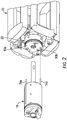
- FIGs. 1 a cross-sectional view of rotating components included in generator 10, according to an embodiment of the present disclosure.
- the generator 10 includes a rotor shaft 12, an exciter rotor 16, a rectifier assembly 18, a resistor pack 20, and a main field winding 22.
- the rotor shaft 12 communicates mechanical energy to the rotating components mounted on the shaft, including the exciter rotor 16, the rectifier assembly 18, the resistor pack 20, and the main field winding 22.
- DC voltage is supplied to the stator windings (not shown) located adjacent to the exciter rotor 16.
- the exciter rotor 16 rotates with the rotor shaft 12, and generates an alternating current (AC) voltage in response to a magnetic field generated by an exciter stator (not shown) located adjacent to the exciter rotor 16.
- the AC voltage is supplied to the rectifier assembly 18, which rectifies the AC voltage to a rectified DC voltage.
- the resistor pack 20 receives the rectified DC voltage, and communicates the rectified DC voltage to the main field winding 22.
- Both the rectifier assembly 18 and the resistor pack 20 are mounted within an inner diameter of the rotor shaft 12, and are therefore subjected to centrifugal forces associated with the rotation of the rotor shaft 12.
- FIG. 2 an exploded view that illustrates the connection of the rectifier assembly 18 to the resistor pack assembly 20 is shown, according to an embodiment of the present disclosure.
- the resistor pack assembly 20 is shown mounted within main field winding 22, but with the rotor shaft 12 removed from the view to prevent obscuration of the resistor pack assembly 20.
- the rectifier assembly 18 includes a first round contact bus bar 74a and a second round contact bus bar 74b extending axially away from rectifier assembly 18.
- the first round contact bus bar 74a and the second round contact bus bar 74b are received by power bands (e.g., power band 70 and power band 73 shown in FIG. 5 ) located within connection orifices 50a and 50b, respectively.
- power bands e.g., power band 70 and power band 73 shown in FIG. 5
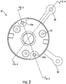
- the resistor pack assembly 20 includes a first DC bus bar 80 and a second DC bus bar 82.
- the first DC bus bar 80 and the second DC bus bar 82 electrically connects to the main field winding 22.
- fasteners 31 utilized to press the components of the resistor pack assembly 20 into abutment with one another, securing those components that are not fastened, as discussed further below.
- the resistor pack assembly 20 includes a resistor housing washer 30, a housing 32, a positive rail 34, a cylindrical suppression resistor 36, an insulator ring 40, and a negative rail 42.
- the negative rail 42 also serves as a structural base for the resistor pack assembly 20.
- Components included within resistor pack assembly 20 are sandwiched in place between resistor housing washer 30 and negative rail 42.
- cylindrical suppression resistor 36 is at least partially located within an internal cavity 32a of the housing 32 interposed between the positive rail 34 and the negative rail 42.
- the housing 32 structurally supports the cylindrical suppression resistor 36.
- the positive rail 34 is also at least partially located within the internal cavity 32a of the housing 32.
- the housing 32 also electrically separates the cylindrical suppression resistor 36 and the positive rail 34 from rotor shaft 12 (shown in FIG. 1 ).
- the suppression resistor 36 provides a ground fault path through rotor shaft 12 that prevents a build-up of charge on the main field windings that can damage the diodes in rectifier assembly 18 when discharged.
- the suppression resistor 36 is a ceramic resistor, although in other embodiments various materials may be employed.
- the resistor pack assembly 20 is held in place via fasteners 31 (e.g., bolts) connected through the resistor housing washer 30, the housing 32, the insulator ring 40, and the negative rail 42. In this way, cylindrical suppression resistor 36 is held in place between the positive rail 34 and the negative rail 42.
- fasteners 31 e.g., bolts
- the resistor pack assembly 20 once again includes the resistor housing washer 30, the housing 32, the positive rail 34, the cylindrical suppression resistor 36, the insulator ring 40, and the negative rail 42.
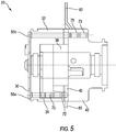
- FIG. 5 illustrates the placement of power band 70 within the connection orifice 50a.
- the connection orifice 50a extends through the resistor housing washer 30, the housing 32, the positive rail 34, and the insulator ring 40, as shown in FIG. 5 .
- the power band 70 is a hollow sleeve that fits within the sleeve-like aperture (e.g., sleeve) 72 of the connection orifice 50a.
- the sleeve-like aperture 50a is located in the positive rail 34.
- the power band 70 is a conductor that is configured to receive the first round contact bus bar 74a (shown in FIG. 2 ) associated with rectifier assembly 18.
- the axial extending connection orifice 50a with the power band 70 allows the rectifier assembly 18 to be electrically connected to the resistor pack 20 simply by sliding the first round contact bus bar 74a (shown in FIG. 2 ) into engagement with power band 70.
- FIG. 5 also illustrates the placement of power band 73 within connection orifice 50b.
- the connection orifice 50a extends through the resistor housing washer 30, the housing 32, the insulator ring 40, and the negative rail 42, as shown in FIG. 5 .
- the power band 73 is a hollow sleeve that fits within the sleeve-like aperture (e.g., sleeve) 75 of the connection orifice 50b.
- the sleeve-like aperture 75 is located in the negative rail 42.
- the power band 73 is a conductor that is configured to receive the second round contact bus bar 74b (shown in FIG. 2 ) associated with rectifier assembly 18.
- the axial extending connection orifice 50b with the power band 73 allows the rectifier assembly 18 to be electrically connected to the resistor pack 20 simply by sliding the second round contact bus bar 74b (shown in FIG. 2 ) into engagement with power band 73.
- resistor pack assembly 20 an exploded view of resistor pack assembly 20 is illustrated, according to an embodiment of the present disclosure.
- the resistor pack assembly 20 once again includes the resistor housing washer 30, the housing 32, the positive rail 34, the cylindrical suppression resistor 36, the insulator ring 40, and the negative rail 42.
- the resistor housing washer 30 includes a plurality of apertures 44 for receiving fasteners 31 (e.g., bolts) for securing components of the resistor pack assembly 20 together.
- the resistor housing washer 30 includes apertures or openings 46 for receiving the first round contact bus bar 74a and the second contact bus bar 74b (shown in FIG. 2 ) associated with rectifier assembly 18.
- the housing 32 is located adjacent to the resistor housing washer 30 and also includes a plurality of apertures 48 for receiving fasteners 31 and/or the first round contact bus bar 74a and the second contact bus bar 74b (shown in FIG. 2 ) associated with the rectifier assembly 18.
- the positive rail 34 is located adjacent to the housing 32, and includes a circular face 34a and a connection terminal 50.
- the positive rail 34 is also located partially within the housing 32, as shown in FIG. 2 .
- the connection terminal 50 extends axially away from the circular face 34a of the positive rail 34.
- the positive rail 34 also includes the sleeve-like aperture (e.g., sleeve) 72 of the connection orifice 50a, as discussed in relation to FIG. 5 above.
- the cylindrical suppression resistor 36 is located between the positive rail 34 and the negative rail 42, as shown in FIGs. 4-6 .
- the cylindrical suppression resistor 36 includes a first flat surface 53a and second flat surface 53b.
- cylindrical suppression resistor 36 is cylindrical, and does not include apertures for receiving a fastener 51. Rather, cylindrical suppression resistor 36 is sandwiched in place between the circular face 34a of the positive rail 34 and an inner circular face 42a of the negative rail 42.
- the contact between the circular face 34a and the first flat surface 53a of the cylindrical suppression resistor 36 provides an electrical connection between the positive rail 34 and cylindrical suppression resistor 36.
- the insulator ring 40 is located adjacent to the housing 32 and the negative rail 42.
- the insulator ring 40 includes a first circular face 40a and a second circular face 40b opposite the first circular face 40a.
- the first face 40 contacts a first face 32b of the housing 32 and the second circular face 40b contacts an outer circular face 42b of the negative rail 42.
- the outer circular face 42b of the negative rail 42 is located radially outward from the inner circular face 42a.
- the cylindrical suppression resistor 36 is located radially inward from the insulator ring 40, as shown in FIG. 2 .
- the insulator ring 40 includes a plurality of apertures 56 for receiving the fasteners 31 provided through the resistor housing washer 30, and the housing 32.
- the fasteners 31 are secured to the negative rail 42 and press the components of resistor pack assembly 20 into abutment with one another, securing those components that are not fastened.
- the insulator ring 40 includes a projection portion 40c that projects away from the second circular face 40b.
- the projection portion 40c mates with a notch 42c located in the negative rail 42 when the components of resistor pack assembly 20 are pressed into abutment with one another.
- the notch 42c is configured to receive the projection portion 40c.
- the insulator ring 40 also includes a first bus bar reception cavity 40g located on a radially outward surface 40f of the projection portion 40c.
- the first bus bar reception cavity 40g is a positive rail/terminal/reception point and the second bus bar reception cavity 42d is a negative rail/terminal/reception point.
- the first bus bar reception cavity 40g is configured to receive a first DC bus bar 80 (see FIG. 2 and 4 ).
- the first DC bus bar 80 is secured within the first bus bar reception cavity 40g.
- the first DC bus bar 80 is at least partially located within the first bus bar reception cavity 40g.
- the first bus bar reception cavity 40 electrically connects the insulator ring 40 to the first DC bus bar 80.
- the insulator ring 40 also includes a receiving orifice 40e located on the first circular face 40a and extending into the insulator ring 40.
- the receiving orifice 40e is configured to receive the connection terminal 50 of the positive rail 34 when the components of resistor pack assembly 20 are pressed into abutment with one another.
- the receiving orifice 40e originates on the first circular face 40a and extends into the insulator ring 40 toward the projection portion 40c.
- by locating the receiving orifice 40e opposite the projection portion 40c increases dielectric separation.
- the electrical current does not flow through the insulator ring 40.
- the electrical current in the resistor pack assembly 20 flows from the first round contact bus bar 74a to the negative rail 42 to the second DC bus bar 82 to the main field winding 22 to the first DC bus bar 80 to the second round contact bus bar 74b.
- the negative rail 42 is located adjacent to the insulator ring 40 and the cylindrical suppression resistor 36.
- the negative rail 42 provides an electrical path to ground (typically a high resistance).
- the rotor shaft 12 is grounded, and the negative rail 42 provides an electrical path to rotor shaft 12 to prevent an undesirable build-up of charge within rectifier assembly 18.
- the negative rail 42 may be composed of a material, such as, for example aluminum alloy, copper alloy, beryllium copper, or aluminum copper alloys.
- the negative rail 42 also includes the sleeve-like aperture (e.g., sleeve) 75 of the connection orifice 50b, as discussed in relation to FIG. 5 above.
- the negative rail 42 also includes a second bus bar reception cavity 42d located on a radially outward surface 42e of the negative rail 42 and extends into the negative rail 42.
- the second bus bar reception cavity 42d is configured to receive a second DC bus bar 82 (see FIG. 3 and 5 ).
- the second DC bus bar 82 is secured within the second bus bar reception cavity 42d.
- the second DC bus bar 82 is at least partially located within the second bus bar reception cavity 42d.
- the second bus bar reception cavity 42d electrically connects the negative rail 42 to the second DC bus bar 82.
- the negative rail 42 includes a plurality of apertures 60 for receiving the fasteners 31 provided through the resistor housing washer 30, the housing 32, and insulator ring 40.
- the fasteners 31 secured to the negative rail 42 and press the components of the resistor pack assembly 20 into abutment with one another, securing those components that are not fastened.
- the fasteners 31 may be secured to the negative rail 42 via anchors 62 located in the apertures 60.
- the anchors 62 may be helical inserts or a threaded insert such as a Keensert.
- the plurality of apertures 44 in the resistor housing washer 30 align with the plurality of apertures 48 in the housing 32, the plurality of apertures 56 in the insulator ring 40, and the plurality of apertures 60 in the negative rail 42.
- the fasteners 31 are located within the plurality of apertures 44 in the resistor housing washer 30, the plurality of apertures 48 in the housing 32, the plurality of apertures 56 in the insulator ring 40, and the plurality of apertures 60 in the negative rail 42.
- FIG. 7 illustrates the engagement of the round contact bus bar 74b associated with the rectifier assembly 18 into the connection orifice 50b.
- the round contact bus bar 74b extends away from the rectifier assembly 18 and engages the connection orifice 50b, making contact with the power band 73 (not shown in this view) located within the connection orifice 50b.
- the round contact bus bar 74a extends away from the rectifier assembly 18 and engages the connection orifice 50a, making contact with the power band 70 located within the connection orifice 50b, as discussed above.
- the round contact bus bar 74b extends through the connection orifice 50b and is engaged within the negative rail 42.
- the purpose of extending the round contact bus bar 74b to make contact with the negative rail 42 is to provide an electrical path between the rectifier assembly 18 and ground (in this case, rotor shaft 12 is grounded).
- the grounded path allows built up static charge on the main field windings to safely discharge in a controlled manner.
- a ground path with resistance limits the amount of static charge that can build up prior to discharge.
- FIG. 7 also illustrates the first DC bus bar 80 extending from resistor pack assembly 20 to main field winding 22.
- the first DC bus bar 80 extends radially outward from the resistor pack assembly 20.
- the first DC bus bar 80 is attached via a nut 82a to main field winding 22.
- FIG. 8 an orthogonal view of the resistor pack assembly 20 mounted within main field winding 22 is illustrated, in accordance with an embodiment of the present disclosure.
- the first DC bus bar 80 and the second DC bus bar 82 are illustrated extending radially outward from the resistor pack assembly 20.
- the first DC bus bar 80 is secured to the main field winding 22 via the first nut 82a and the second DC bus bar 82 is secured to the main field winding 22 via the second nut 82b, respectively, for electrical connection to the main field winding 22.
Landscapes
- Engineering & Computer Science (AREA)
- Microelectronics & Electronic Packaging (AREA)
- Power Engineering (AREA)
- Synchronous Machinery (AREA)
Description
- The subject matter disclosed herein generally relates to generators, and more specifically to a rotating resistor pack employed in a generator.
- A typical generator assembly includes a rotor portion and a stator portion. Mechanical energy is provided to the generator via a shaft connected to the rotor portion that is converted into electrical energy that is provided via the stator portion. Such a generator with a resistor pack assembly is known from
US2013/0300231A1 . - Many generators take advantage of three stages, including a permanent magnet stage, an exciter stage and a main stage. The exciter stage includes an exciter stator winding for receiving direct current (DC) power that energizes the exciter stator and generates the desired magnetic field. Rotational energy provided by the shaft causes the exciter rotor to move through the magnetic field, resulting in the generation of alternating current (AC) electric power in the exciter rotor. A rotating rectifier assembly is mounted within the rotor for converting the AC power to DC electric power that is supplied to the main rotor winding. The DC power provided to the rotating main rotor winding results in a rotating magnetic field that generates AC power in the stator windings.
- Suppression resistors may also be included within or nearby the rotating rectifier assembly to provide an alternate path for voltage and current transients and protect the rotating rectifier assembly. However, the rotating rectifier assembly and the suppression resistors are mounted on the rotating shaft, and are therefore subject to the centrifugal forces associated with the rotating shaft.
- According to one embodiment, a resistor pack assembly is provided as defined by
claim 1. - In addition to one or more of the features described above, or as an alternative, further embodiments may include that the first DC bus bar extends radially outward from the insulator ring.
- In addition to one or more of the features described above, or as an alternative, further embodiments may include that the second DC bus bar extends radially outward from the negative rail.
- [DELETED]
- In addition to one or more of the features described above, or as an alternative, further embodiments may include that the negative rail includes a second bus bar reception cavity located on a radially outward surface of the negative rail and extending into the negative rail, the second DC bus bar being at least partially located within the second bus bar reception cavity.
- [DELETED]
- In addition to one or more of the features described above, or as an alternative, further embodiments may include that the insulator ring includes a projection portion that projects away from the second circular face and the negative rail includes a notch configured to receive the projection portion, and wherein the first bus bar reception cavity located on a radially outward surface of the projection portion of the insulator ring.
- [DELETED]
- In addition to one or more of the features described above, or as an alternative, further embodiments may include that the receiving orifice is located on the first circular face opposite the projection portion.
- In addition to one or more of the features described above, or as an alternative, further embodiments may include that the positive rail includes a connection terminal and the insulator ring includes a receiving orifice located on the first circular face and extending into the insulator ring, the receiving orifice being configured to receive the connection terminal.
- In addition to one or more of the features described above, or as an alternative, further embodiments may include: a connection orifice that extends through the positive rail and the insulator ring; and a power band located within the connection orifice within the positive rail.
- In addition to one or more of the features described above, or as an alternative, further embodiments may include: a connection orifice that extends through the insulator ring and the negative rail; and a power band located within the connection orifice within the negative rail.
- In addition to one or more of the features described above, or as an alternative, further embodiments may include: a housing having an internal cavity and a first face, wherein the positive rail and the cylindrical suppression resistor are at least partially located within the internal cavity and the first circular face of the insulator ring contacts the first face of the housing.
- In addition to one or more of the features described above, or as an alternative, further embodiments may include: a resistor housing washer having a plurality of apertures for receiving a fastener, the plurality of apertures in the resistor housing washer align with a plurality of apertures in the housing, a plurality of apertures in the insulator ring, and a plurality of apertures in the negative rail.
- According to another embodiment, a generator having a plurality of rotating components that rectify an alternating current (AC) voltage to a direct current (DC) voltage supplied to main field windings is provided. The generator including: a rotor shaft having an inner diameter; a rectifier assembly located within the inner diameter of the rotor shaft and connected to convert the AC voltage to a rectified DC voltage supplied via a first round contact bus bar that extends axially away from the rectifier assembly and a second round contact bus bar that extends axially away from the rectifier assembly; and a resistor pack assembly located axially adjacent to the rectifier assembly and within the inner diameter of the rotor shaft, wherein the resistor pack assembly receives the DC voltage supplied by the first round contact bus bar and the second round contact bus bar, wherein the resistor pack assembly communicates the DC voltage to a main field winding, and wherein the resistor pack assembly includes: a positive rail having a circular face; a negative rail having an inner circular face and an outer circular face located radially outward from the inner circular face; an insulator ring having a first circular face and a second circular face opposite the first circular face, the second circular face contacts the outer circular face of the negative rail; a first DC bus bar electrically connected to the insulator ring; a second DC bus bar electrically connected to the negative rail; and a cylindrical suppression resistor having a first flat surface and a second flat surface opposite the first flat surface, the cylindrical suppression resistor is located radially inward of the insulator and axially between the positive rail and the negative rail, wherein the first flat surface contacts the circular face of the positive rail and the second flat surface contacts the inner circular face of the negative rail.
- In addition to one or more of the features described above, or as an alternative, further embodiments may include that the first DC bus bar extends radially outward from the insulator ring and is electrically connected to the main field winding.
- In addition to one or more of the features described above, or as an alternative, further embodiments may include that the second DC bus bar extends radially outward from the negative rail and is electrically connected to the main field winding.
- In addition to one or more of the features described above, or as an alternative, further embodiments may include that the insulator ring includes a first bus bar reception cavity located on a radially outward surface of the insulator ring and extending into the insulator ring, the first DC bus bar being at least partially located within the first bus bar reception cavity.
- In addition to one or more of the features described above, or as an alternative, further embodiments may include that the negative rail includes a second bus bar reception cavity located on a radially outward surface of the negative rail and extending into the negative rail, the second DC bus bar being at least partially located within the second bus bar reception cavity.
- In addition to one or more of the features described above, or as an alternative, further embodiments may include that the insulator ring includes a projection portion that projects away from the second circular face and the negative rail includes a notch configured to receive the projection portion.
- The foregoing features and elements may be combined in various combinations without exclusivity, unless expressly indicated otherwise. These features and elements as well as the operation thereof will become more apparent in light of the following description and the accompanying drawings. It should be understood, however, that the following description and drawings are intended to be illustrative and explanatory in nature and non-limiting.
- The following descriptions should not be considered limiting in any way. With reference to the accompanying drawings, like elements are numbered alike:
-
FIG. 1 is a cross-sectional view of rotating components included in a variable frequency generator, according to an embodiment of the present disclosure; -
FIG. 2 is an exploded view that illustrates the connection of a rectifier assembly to a resistor pack assembly of the variable frequency generator ofFIG. 1 , according to an embodiment of the present disclosure; -
FIG. 3 is an axial view the resistor pack assembly, according to an embodiment of the present disclosure; -
FIG. 4 is an cross-sectional view the resistor pack assembly, according to an embodiment of the present disclosure; -
FIG. 5 is an cross-sectional view the resistor pack assembly, according to an embodiment of the present disclosure; -
FIG. 6 is an exploded view the resistor pack assembly, according to an embodiment of the present disclosure; -
FIG. 7 is a cross-sectional view of rotating components included in a variable frequency generator, according to an embodiment of the present disclosure; and -
FIG. 8 is an orthogonal view of the assembled connection of the resistor pack assembly to the rotor field winding, according to an embodiment of the present disclosure. - A detailed description of one or more embodiments of the disclosed apparatus and method are presented herein by way of exemplification and not limitation with reference to the Figures.
- Referring now to
FIGs. 1 , a cross-sectional view of rotating components included ingenerator 10, according to an embodiment of the present disclosure. Thegenerator 10 includes arotor shaft 12, anexciter rotor 16, arectifier assembly 18, aresistor pack 20, and a main field winding 22. Therotor shaft 12 communicates mechanical energy to the rotating components mounted on the shaft, including theexciter rotor 16, therectifier assembly 18, theresistor pack 20, and the main field winding 22. - DC voltage is supplied to the stator windings (not shown) located adjacent to the
exciter rotor 16. Theexciter rotor 16 rotates with therotor shaft 12, and generates an alternating current (AC) voltage in response to a magnetic field generated by an exciter stator (not shown) located adjacent to theexciter rotor 16. The AC voltage is supplied to therectifier assembly 18, which rectifies the AC voltage to a rectified DC voltage. Theresistor pack 20 receives the rectified DC voltage, and communicates the rectified DC voltage to the main field winding 22. - Both the
rectifier assembly 18 and theresistor pack 20 are mounted within an inner diameter of therotor shaft 12, and are therefore subjected to centrifugal forces associated with the rotation of therotor shaft 12. A benefit of locating therectifier assembly 18 and theresistor pack 20 within the inner diameter of therotor shaft 12, is therectifier assembly 18 and theresistor pack 20 are structurally supported by therotor shaft 12. Locating components within the inner diameter (ID) of therotor shaft 12 forces therotor shaft 12 to a certain size to accommodate the components and adds to the stiffness of therotor shaft 12. Increased shaft stiffness increases a maximum obtainable speed of therotor shaft 12. - Referring now to
FIG. 2 , with continued reference toFIG. 1 , an exploded view that illustrates the connection of therectifier assembly 18 to theresistor pack assembly 20 is shown, according to an embodiment of the present disclosure. In the embodiment shown inFIG. 2 , theresistor pack assembly 20 is shown mounted within main field winding 22, but with therotor shaft 12 removed from the view to prevent obscuration of theresistor pack assembly 20. Therectifier assembly 18 includes a first roundcontact bus bar 74a and a second roundcontact bus bar 74b extending axially away fromrectifier assembly 18. As described below, the first roundcontact bus bar 74a and the second roundcontact bus bar 74b are received by power bands (e.g.,power band 70 andpower band 73 shown inFIG. 5 ) located withinconnection orifices - Referring now to
FIG. 3 , with continued reference toFIGs. 1-2 , an axial view of theresistor pack assembly 20 is illustrated, in accordance with an embodiment of the present discloser. In the embodiment shown inFIG. 3 , theresistor pack assembly 20 includes a firstDC bus bar 80 and a secondDC bus bar 82. The firstDC bus bar 80 and the secondDC bus bar 82 electrically connects to the main field winding 22. Also visible inFIG. 3 arefasteners 31 utilized to press the components of theresistor pack assembly 20 into abutment with one another, securing those components that are not fastened, as discussed further below. - Referring now to
FIG. 4 , with continuedFIG. 1-3 , a cross-sectional view of theresistor pack assembly 20 is illustrated, according to an embodiment of the present disclosure. Theresistor pack assembly 20 includes aresistor housing washer 30, ahousing 32, apositive rail 34, acylindrical suppression resistor 36, aninsulator ring 40, and anegative rail 42. Thenegative rail 42 also serves as a structural base for theresistor pack assembly 20. Components included withinresistor pack assembly 20 are sandwiched in place betweenresistor housing washer 30 andnegative rail 42. In particular,cylindrical suppression resistor 36 is at least partially located within aninternal cavity 32a of thehousing 32 interposed between thepositive rail 34 and thenegative rail 42. Thehousing 32 structurally supports thecylindrical suppression resistor 36. Thepositive rail 34 is also at least partially located within theinternal cavity 32a of thehousing 32. Thehousing 32 also electrically separates thecylindrical suppression resistor 36 and thepositive rail 34 from rotor shaft 12 (shown inFIG. 1 ). - The
suppression resistor 36 provides a ground fault path throughrotor shaft 12 that prevents a build-up of charge on the main field windings that can damage the diodes inrectifier assembly 18 when discharged. In the embodiment, thesuppression resistor 36 is a ceramic resistor, although in other embodiments various materials may be employed. - The
resistor pack assembly 20 is held in place via fasteners 31 (e.g., bolts) connected through theresistor housing washer 30, thehousing 32, theinsulator ring 40, and thenegative rail 42. In this way,cylindrical suppression resistor 36 is held in place between thepositive rail 34 and thenegative rail 42. - Referring now to
FIG. 5 , with continuedFIG. 1-4 , a cross-sectional view of theresistor pack assembly 20 is illustrated, according to an embodiment of the present disclosure. Theresistor pack assembly 20 once again includes theresistor housing washer 30, thehousing 32, thepositive rail 34, thecylindrical suppression resistor 36, theinsulator ring 40, and thenegative rail 42. -
FIG. 5 illustrates the placement ofpower band 70 within theconnection orifice 50a. Theconnection orifice 50a extends through theresistor housing washer 30, thehousing 32, thepositive rail 34, and theinsulator ring 40, as shown inFIG. 5 . Thepower band 70 is a hollow sleeve that fits within the sleeve-like aperture (e.g., sleeve) 72 of theconnection orifice 50a. The sleeve-like aperture 50a is located in thepositive rail 34. Thepower band 70 is a conductor that is configured to receive the first roundcontact bus bar 74a (shown inFIG. 2 ) associated withrectifier assembly 18. The axial extendingconnection orifice 50a with thepower band 70 allows therectifier assembly 18 to be electrically connected to theresistor pack 20 simply by sliding the first roundcontact bus bar 74a (shown inFIG. 2 ) into engagement withpower band 70. -
FIG. 5 also illustrates the placement ofpower band 73 withinconnection orifice 50b. Theconnection orifice 50a extends through theresistor housing washer 30, thehousing 32, theinsulator ring 40, and thenegative rail 42, as shown inFIG. 5 . Thepower band 73 is a hollow sleeve that fits within the sleeve-like aperture (e.g., sleeve) 75 of theconnection orifice 50b. The sleeve-like aperture 75 is located in thenegative rail 42. Thepower band 73 is a conductor that is configured to receive the second roundcontact bus bar 74b (shown inFIG. 2 ) associated withrectifier assembly 18. The axial extendingconnection orifice 50b with thepower band 73 allows therectifier assembly 18 to be electrically connected to theresistor pack 20 simply by sliding the second roundcontact bus bar 74b (shown inFIG. 2 ) into engagement withpower band 73. - Referring now to
FIG. 6 , with continued reference toFIGs. 1-5 , an exploded view ofresistor pack assembly 20 is illustrated, according to an embodiment of the present disclosure. In the embodiment shown inFIG. 6 , theresistor pack assembly 20 once again includes theresistor housing washer 30, thehousing 32, thepositive rail 34, thecylindrical suppression resistor 36, theinsulator ring 40, and thenegative rail 42. - The
resistor housing washer 30 includes a plurality ofapertures 44 for receiving fasteners 31 (e.g., bolts) for securing components of theresistor pack assembly 20 together. In addition, theresistor housing washer 30 includes apertures oropenings 46 for receiving the first roundcontact bus bar 74a and the secondcontact bus bar 74b (shown inFIG. 2 ) associated withrectifier assembly 18. Thehousing 32 is located adjacent to theresistor housing washer 30 and also includes a plurality ofapertures 48 for receivingfasteners 31 and/or the first roundcontact bus bar 74a and the secondcontact bus bar 74b (shown inFIG. 2 ) associated with therectifier assembly 18. - The
positive rail 34 is located adjacent to thehousing 32, and includes acircular face 34a and aconnection terminal 50. Thepositive rail 34 is also located partially within thehousing 32, as shown inFIG. 2 . Theconnection terminal 50 extends axially away from thecircular face 34a of thepositive rail 34. Thepositive rail 34 also includes the sleeve-like aperture (e.g., sleeve) 72 of theconnection orifice 50a, as discussed in relation toFIG. 5 above. - The
cylindrical suppression resistor 36 is located between thepositive rail 34 and thenegative rail 42, as shown inFIGs. 4-6 . Thecylindrical suppression resistor 36 includes a firstflat surface 53a and secondflat surface 53b. In the embodiment shown inFIG. 3 ,cylindrical suppression resistor 36 is cylindrical, and does not include apertures for receiving a fastener 51. Rather,cylindrical suppression resistor 36 is sandwiched in place between thecircular face 34a of thepositive rail 34 and an innercircular face 42a of thenegative rail 42. In addition, the contact between thecircular face 34a and the firstflat surface 53a of thecylindrical suppression resistor 36 provides an electrical connection between thepositive rail 34 andcylindrical suppression resistor 36. - The
insulator ring 40 is located adjacent to thehousing 32 and thenegative rail 42. Theinsulator ring 40 includes a firstcircular face 40a and a secondcircular face 40b opposite the firstcircular face 40a. Thefirst face 40 contacts afirst face 32b of thehousing 32 and the secondcircular face 40b contacts an outercircular face 42b of thenegative rail 42. The outercircular face 42b of thenegative rail 42 is located radially outward from the innercircular face 42a. Thecylindrical suppression resistor 36 is located radially inward from theinsulator ring 40, as shown inFIG. 2 . - The
insulator ring 40 includes a plurality ofapertures 56 for receiving thefasteners 31 provided through theresistor housing washer 30, and thehousing 32. Thefasteners 31 are secured to thenegative rail 42 and press the components ofresistor pack assembly 20 into abutment with one another, securing those components that are not fastened. - The
insulator ring 40 includes a projection portion 40c that projects away from the secondcircular face 40b. The projection portion 40c mates with anotch 42c located in thenegative rail 42 when the components ofresistor pack assembly 20 are pressed into abutment with one another. Thenotch 42c is configured to receive the projection portion 40c. Theinsulator ring 40 also includes a first bus bar reception cavity 40g located on a radiallyoutward surface 40f of the projection portion 40c. In an embodiment, the first bus bar reception cavity 40g is a positive rail/terminal/reception point and the second busbar reception cavity 42d is a negative rail/terminal/reception point. The first bus bar reception cavity 40g is configured to receive a first DC bus bar 80 (seeFIG. 2 and4 ). The firstDC bus bar 80 is secured within the first bus bar reception cavity 40g. The firstDC bus bar 80 is at least partially located within the first bus bar reception cavity 40g. The first busbar reception cavity 40 electrically connects theinsulator ring 40 to the firstDC bus bar 80. - The
insulator ring 40 also includes a receivingorifice 40e located on the firstcircular face 40a and extending into theinsulator ring 40. The receivingorifice 40e is configured to receive theconnection terminal 50 of thepositive rail 34 when the components ofresistor pack assembly 20 are pressed into abutment with one another. The receivingorifice 40e originates on the firstcircular face 40a and extends into theinsulator ring 40 toward the projection portion 40c. Advantageously, by locating the receivingorifice 40e opposite the projection portion 40c increases dielectric separation. The electrical current does not flow through theinsulator ring 40. The electrical current in theresistor pack assembly 20 flows from the first roundcontact bus bar 74a to thenegative rail 42 to the secondDC bus bar 82 to the main field winding 22 to the firstDC bus bar 80 to the second roundcontact bus bar 74b. - The
negative rail 42 is located adjacent to theinsulator ring 40 and thecylindrical suppression resistor 36. Thenegative rail 42 provides an electrical path to ground (typically a high resistance). In an embodiment, therotor shaft 12 is grounded, and thenegative rail 42 provides an electrical path torotor shaft 12 to prevent an undesirable build-up of charge withinrectifier assembly 18. Thenegative rail 42 may be composed of a material, such as, for example aluminum alloy, copper alloy, beryllium copper, or aluminum copper alloys. Thenegative rail 42 also includes the sleeve-like aperture (e.g., sleeve) 75 of theconnection orifice 50b, as discussed in relation toFIG. 5 above. - The
negative rail 42 also includes a second busbar reception cavity 42d located on a radiallyoutward surface 42e of thenegative rail 42 and extends into thenegative rail 42. The second busbar reception cavity 42d is configured to receive a second DC bus bar 82 (seeFIG. 3 and5 ). The secondDC bus bar 82 is secured within the second busbar reception cavity 42d. The secondDC bus bar 82 is at least partially located within the second busbar reception cavity 42d. The second busbar reception cavity 42d electrically connects thenegative rail 42 to the secondDC bus bar 82. - The
negative rail 42 includes a plurality ofapertures 60 for receiving thefasteners 31 provided through theresistor housing washer 30, thehousing 32, andinsulator ring 40. Thefasteners 31 secured to thenegative rail 42 and press the components of theresistor pack assembly 20 into abutment with one another, securing those components that are not fastened. Thefasteners 31 may be secured to thenegative rail 42 viaanchors 62 located in theapertures 60. In an embodiment, theanchors 62 may be helical inserts or a threaded insert such as a Keensert. The plurality ofapertures 44 in theresistor housing washer 30 align with the plurality ofapertures 48 in thehousing 32, the plurality ofapertures 56 in theinsulator ring 40, and the plurality ofapertures 60 in thenegative rail 42. Thefasteners 31 are located within the plurality ofapertures 44 in theresistor housing washer 30, the plurality ofapertures 48 in thehousing 32, the plurality ofapertures 56 in theinsulator ring 40, and the plurality ofapertures 60 in thenegative rail 42. - Referring now to
FIG. 7 , with continued reference toFIG. 1-6 , a cross-sectional view of the assembled connection of therectifier assembly 18 to theresistor pack assembly 20 is illustrated, according to an embodiment of the present disclosure. In particular,FIG. 7 illustrates the engagement of the roundcontact bus bar 74b associated with therectifier assembly 18 into theconnection orifice 50b. The roundcontact bus bar 74b extends away from therectifier assembly 18 and engages theconnection orifice 50b, making contact with the power band 73 (not shown in this view) located within theconnection orifice 50b. Likewise, although not shown inFIG. 7 , the roundcontact bus bar 74a extends away from therectifier assembly 18 and engages theconnection orifice 50a, making contact with thepower band 70 located within theconnection orifice 50b, as discussed above. - In addition, the round
contact bus bar 74b extends through theconnection orifice 50b and is engaged within thenegative rail 42. The purpose of extending the roundcontact bus bar 74b to make contact with thenegative rail 42 is to provide an electrical path between therectifier assembly 18 and ground (in this case,rotor shaft 12 is grounded). The grounded path allows built up static charge on the main field windings to safely discharge in a controlled manner. A ground path with resistance limits the amount of static charge that can build up prior to discharge. -
FIG. 7 also illustrates the firstDC bus bar 80 extending fromresistor pack assembly 20 to main field winding 22. In the embodiment shown inFIG. 7 , the firstDC bus bar 80 extends radially outward from theresistor pack assembly 20. The firstDC bus bar 80 is attached via anut 82a to main field winding 22. - Referring now to
FIG. 8 , with continued reference toFIG. 1-7 , an orthogonal view of theresistor pack assembly 20 mounted within main field winding 22 is illustrated, in accordance with an embodiment of the present disclosure. The firstDC bus bar 80 and the secondDC bus bar 82 are illustrated extending radially outward from theresistor pack assembly 20. The firstDC bus bar 80 is secured to the main field winding 22 via thefirst nut 82a and the secondDC bus bar 82 is secured to the main field winding 22 via thesecond nut 82b, respectively, for electrical connection to the main field winding 22. - The term "about" is intended to include the degree of error associated with measurement of the particular quantity based upon the equipment available at the time of filing the application. For example, "about" can include a range of ± 8% or 5%, or 2% of a given value.
- The terminology used herein is for the purpose of describing particular embodiments only and is not intended to be limiting of the present disclosure. As used herein, the singular forms "a", "an" and "the" are intended to include the plural forms as well, unless the context clearly indicates otherwise. It will be further understood that the terms "comprises" and/or "comprising," when used in this specification, specify the presence of stated features, integers, steps, operations, elements, and/or components, but do not preclude the presence or addition of one or more other features, integers, steps, operations, element components, and/or groups thereof.
- While the present disclosure has been described with reference to an exemplary embodiment or embodiments, it will be understood by those skilled in the art that various changes may be made. In addition, many modifications may be made to adapt a particular situation or material to the teachings of the present disclosure without departing from the scope of the invention. Therefore, it is intended that the present disclosure not be limited to the particular embodiment disclosed as the best mode contemplated for carrying out this present disclosure, but that the present disclosure will include all embodiments falling within the scope of the claims.
Claims (10)
- A resistor pack assembly comprising:a positive rail (34) having a circular face (34a);a negative rail (42) having an inner circular face (42a) and an outer circular face (42b) located radially outward from the inner circular face;an insulator ring (40) having a first circular face (40a) and a second circular face (40b) opposite the first circular face, the second circular face contacts the outer circular face of the negative rail, wherein the insulator ring (40) includes a projection portion (40c) that projects away from the second circular face and the negative rail includes a notch (42c) configured to receive the projection portion, wherein the insulator ring (40) includes a first bus bar reception cavity (40g) located on a radially outward surface (40f) of the projection portion (40c) and extending into the insulator ring (40);a first DC bus bar (80) at least partially located within the first bus bar reception cavity (40g);a second DC bus bar (82) electrically connected to the negative rail; anda cylindrical suppression resistor (36) having a first flat surface (53a) and a second flat surface (53b) opposite the first flat surface, the cylindrical suppression resistor is located radially inward of the insulator and axially between the positive rail and the negative rail, wherein the first flat surface contacts the circular face of the positive rail and the second flat surface contacts the inner circular face of the negative rail,wherein the positive rail (34) includes a connection terminal (50) and the insulator ring (40) includes a receiving orifice (40e) located on the first circular face and extending into the insulator ring, the receiving orifice being configured to receive the connection terminal.
- The resistor pack assembly of claim 1, wherein the first DC bus bar (80) extends radially outward from the insulator ring (40).
- The resistor pack assembly of claim 1 or 2, wherein the second DC bus bar (82) extends radially outward from the negative rail (42).
- The resistor pack assembly of any preceding claim, wherein the negative rail includes a second bus bar reception cavity (42d) located on a radially outward surface of the negative rail and extending into the negative rail, the second DC bus bar being at least partially located within the second bus bar reception cavity.
- The resistor pack assembly of any preceding claim, wherein the receiving orifice (40e) is located on the first circular face opposite the projection portion.
- The resistor pack assembly of any preceding claim, further comprising:a connection orifice (50a) that extends through the positive rail (34) and the insulator ring (40); anda power band (70) located within the connection orifice within the positive rail.
- The resistor pack assembly of any preceding claim, further comprising:a connection orifice (50b) that extends through the insulator ring and the negative rail; anda power band (73) located within the connection orifice within the negative rail.
- 9. The resistor pack assembly of any preceding claim, further comprising:
a housing (32) having an internal cavity (32a) and a first face (32b), wherein the positive rail and the cylindrical suppression resistor are at least partially located within the internal cavity and the first circular face of the insulator ring contacts the first face of the housing. - The resistor pack assembly of claim 8 further comprising:
a resistor housing washer (30) having a plurality of apertures (48) for receiving a fastener (31), the plurality of apertures in the resistor housing washer align with a plurality of apertures in the housing, a plurality of apertures in the insulator ring, and a plurality of apertures in the negative rail. - A generator having a plurality of rotating components that rectify an alternating current (AC) voltage to a direct current (DC) voltage supplied to main field windings, the generator comprising:a rotor shaft (12) having an inner diameter;a rectifier assembly (18) located within the inner diameter of the rotor shaft and connected to convert the AC voltage to a rectified DC voltage supplied via a first round contact bus bar that extends axially away from the rectifier assembly and a second round contact bus bar that extends axially away from the rectifier assembly; anda resistor pack assembly (20) as claimed in any preceding claim located axially adjacent to the rectifier assembly and within the inner diameter of the rotor shaft, wherein the resistor pack assembly receives the DC voltage supplied by the first round contact bus bar and the second round contact bus bar, wherein the resistor pack assembly communicates the DC voltage to a main field winding.
Applications Claiming Priority (1)
| Application Number | Priority Date | Filing Date | Title |
|---|---|---|---|
| US16/173,324 US10460861B1 (en) | 2018-10-29 | 2018-10-29 | High speed rotor connection assembly |
Publications (2)
| Publication Number | Publication Date |
|---|---|
| EP3648317A1 EP3648317A1 (en) | 2020-05-06 |
| EP3648317B1 true EP3648317B1 (en) | 2022-01-12 |
Family
ID=68314780
Family Applications (1)
| Application Number | Title | Priority Date | Filing Date |
|---|---|---|---|
| EP19205868.3A Active EP3648317B1 (en) | 2018-10-29 | 2019-10-29 | High speed rotor connection assembly |
Country Status (2)
| Country | Link |
|---|---|
| US (1) | US10460861B1 (en) |
| EP (1) | EP3648317B1 (en) |
Families Citing this family (7)
| Publication number | Priority date | Publication date | Assignee | Title |
|---|---|---|---|---|
| US11139723B2 (en) * | 2017-04-28 | 2021-10-05 | Hamilton Sundstrand Corporation | Rotating rectifier assembly |
| US10879772B2 (en) * | 2019-01-08 | 2020-12-29 | Hamilton Sundstrand Corporation | Rotating resistor assemblies |
| US11374456B2 (en) * | 2019-08-01 | 2022-06-28 | Hamilton Sundstrand Corporation | Generator main field connection |
| US11539270B2 (en) | 2020-03-13 | 2022-12-27 | Hamilton Sundstrand Corporation | Connection assembly cover with integrated anti-rotation |
| US11949294B2 (en) * | 2021-03-13 | 2024-04-02 | Hamilton Sundstrand Corporation | Resistor plate assembly with contact bands |
| US12009126B2 (en) * | 2021-03-13 | 2024-06-11 | Hamilton Sundstrand Corporation | Resistor support assembly with spring seat |
| US11799391B2 (en) | 2021-03-13 | 2023-10-24 | Hamilton Sundstrand Corporation | Diode mounting ring with contact band inserts |
Family Cites Families (5)
| Publication number | Priority date | Publication date | Assignee | Title |
|---|---|---|---|---|
| US7944100B2 (en) * | 2009-05-06 | 2011-05-17 | Hamilton Sundstrand Corporation | Generator rectifier assembly with ease of assembly features |
| CN103931081B (en) * | 2011-06-10 | 2018-11-13 | 艾克西弗拉克斯控股有限公司 | Motor/generator |
| US9035508B2 (en) * | 2012-05-08 | 2015-05-19 | Hamilton Sundstrand Corporation | Rotating resistor assembly |
| US9312742B2 (en) * | 2013-03-01 | 2016-04-12 | Hamilton Sundstrand Corporation | Connector and spring assembly for a generator |
| US11139723B2 (en) * | 2017-04-28 | 2021-10-05 | Hamilton Sundstrand Corporation | Rotating rectifier assembly |
-
2018
- 2018-10-29 US US16/173,324 patent/US10460861B1/en active Active
-
2019
- 2019-10-29 EP EP19205868.3A patent/EP3648317B1/en active Active
Also Published As
| Publication number | Publication date |
|---|---|
| EP3648317A1 (en) | 2020-05-06 |
| US10460861B1 (en) | 2019-10-29 |
Similar Documents
| Publication | Publication Date | Title |
|---|---|---|
| EP3648317B1 (en) | High speed rotor connection assembly | |
| US9035508B2 (en) | Rotating resistor assembly | |
| EP1425838B1 (en) | Rotor assembly with hub | |
| EP0426376A2 (en) | Switched reluctance motor rotor | |
| US8063522B2 (en) | Generator rotor ground bushing | |
| US20030048015A1 (en) | System and method for retaining wedges in a rotor | |
| US20050218740A1 (en) | Low profile generator configuration | |
| US20140210320A1 (en) | Electric machine and rectifier assembly therefor | |
| US11245312B2 (en) | High speed generator connection assembly | |
| US6661135B2 (en) | Multi-pole high speed generator with a modular rectifier circuit | |
| EP3681020B1 (en) | Rotating resistor assemblies | |
| US6859019B2 (en) | System and method for coupling rectifiers of an exciter to the rotor of a main generator | |
| US4827165A (en) | Integrated diode package | |
| EP3879682B1 (en) | Connection assembly cover with integrated anti-rotation | |
| US6879083B2 (en) | Generator rotor coil end-turn retention system and method | |
| EP3866314B1 (en) | Rotating rectifier assemblies, generators having rotating rectifier assemblies, and methods of making rotating rectifier assemblies | |
| CN108288879B (en) | Stator support for an electric machine | |
| EP3716445B1 (en) | Generators and methods of making generators | |
| EP3544157A1 (en) | Rotor and motor having the same | |
| US2575932A (en) | Dynamoelectric machine rotor and winding | |
| US20240322634A1 (en) | Electrical machine having a lead retention assembly | |
| EP3709483A1 (en) | Rotor assembly |
Legal Events
| Date | Code | Title | Description |
|---|---|---|---|
| PUAI | Public reference made under article 153(3) epc to a published international application that has entered the european phase |
Free format text: ORIGINAL CODE: 0009012 |
|
| STAA | Information on the status of an ep patent application or granted ep patent |
Free format text: STATUS: THE APPLICATION HAS BEEN PUBLISHED |
|
| AK | Designated contracting states |
Kind code of ref document: A1 Designated state(s): AL AT BE BG CH CY CZ DE DK EE ES FI FR GB GR HR HU IE IS IT LI LT LU LV MC MK MT NL NO PL PT RO RS SE SI SK SM TR |
|
| AX | Request for extension of the european patent |
Extension state: BA ME |
|
| STAA | Information on the status of an ep patent application or granted ep patent |
Free format text: STATUS: REQUEST FOR EXAMINATION WAS MADE |
|
| 17P | Request for examination filed |
Effective date: 20201106 |
|
| RBV | Designated contracting states (corrected) |
Designated state(s): AL AT BE BG CH CY CZ DE DK EE ES FI FR GB GR HR HU IE IS IT LI LT LU LV MC MK MT NL NO PL PT RO RS SE SI SK SM TR |
|
| GRAP | Despatch of communication of intention to grant a patent |
Free format text: ORIGINAL CODE: EPIDOSNIGR1 |
|
| STAA | Information on the status of an ep patent application or granted ep patent |
Free format text: STATUS: GRANT OF PATENT IS INTENDED |
|
| INTG | Intention to grant announced |
Effective date: 20210906 |
|
| GRAS | Grant fee paid |
Free format text: ORIGINAL CODE: EPIDOSNIGR3 |
|
| GRAA | (expected) grant |
Free format text: ORIGINAL CODE: 0009210 |
|
| STAA | Information on the status of an ep patent application or granted ep patent |
Free format text: STATUS: THE PATENT HAS BEEN GRANTED |
|
| AK | Designated contracting states |
Kind code of ref document: B1 Designated state(s): AL AT BE BG CH CY CZ DE DK EE ES FI FR GB GR HR HU IE IS IT LI LT LU LV MC MK MT NL NO PL PT RO RS SE SI SK SM TR |
|
| REG | Reference to a national code |
Ref country code: GB Ref legal event code: FG4D |
|
| REG | Reference to a national code |
Ref country code: CH Ref legal event code: EP |
|
| REG | Reference to a national code |
Ref country code: DE Ref legal event code: R096 Ref document number: 602019010851 Country of ref document: DE |
|
| REG | Reference to a national code |
Ref country code: IE Ref legal event code: FG4D |
|
| REG | Reference to a national code |
Ref country code: AT Ref legal event code: REF Ref document number: 1463034 Country of ref document: AT Kind code of ref document: T Effective date: 20220215 |
|
| REG | Reference to a national code |
Ref country code: LT Ref legal event code: MG9D |
|
| REG | Reference to a national code |
Ref country code: NL Ref legal event code: MP Effective date: 20220112 |
|
| REG | Reference to a national code |
Ref country code: AT Ref legal event code: MK05 Ref document number: 1463034 Country of ref document: AT Kind code of ref document: T Effective date: 20220112 |
|
| PG25 | Lapsed in a contracting state [announced via postgrant information from national office to epo] |
Ref country code: NL Free format text: LAPSE BECAUSE OF FAILURE TO SUBMIT A TRANSLATION OF THE DESCRIPTION OR TO PAY THE FEE WITHIN THE PRESCRIBED TIME-LIMIT Effective date: 20220112 |
|
| PG25 | Lapsed in a contracting state [announced via postgrant information from national office to epo] |
Ref country code: SE Free format text: LAPSE BECAUSE OF FAILURE TO SUBMIT A TRANSLATION OF THE DESCRIPTION OR TO PAY THE FEE WITHIN THE PRESCRIBED TIME-LIMIT Effective date: 20220112 Ref country code: RS Free format text: LAPSE BECAUSE OF FAILURE TO SUBMIT A TRANSLATION OF THE DESCRIPTION OR TO PAY THE FEE WITHIN THE PRESCRIBED TIME-LIMIT Effective date: 20220112 Ref country code: PT Free format text: LAPSE BECAUSE OF FAILURE TO SUBMIT A TRANSLATION OF THE DESCRIPTION OR TO PAY THE FEE WITHIN THE PRESCRIBED TIME-LIMIT Effective date: 20220512 Ref country code: NO Free format text: LAPSE BECAUSE OF FAILURE TO SUBMIT A TRANSLATION OF THE DESCRIPTION OR TO PAY THE FEE WITHIN THE PRESCRIBED TIME-LIMIT Effective date: 20220412 Ref country code: LT Free format text: LAPSE BECAUSE OF FAILURE TO SUBMIT A TRANSLATION OF THE DESCRIPTION OR TO PAY THE FEE WITHIN THE PRESCRIBED TIME-LIMIT Effective date: 20220112 Ref country code: HR Free format text: LAPSE BECAUSE OF FAILURE TO SUBMIT A TRANSLATION OF THE DESCRIPTION OR TO PAY THE FEE WITHIN THE PRESCRIBED TIME-LIMIT Effective date: 20220112 Ref country code: ES Free format text: LAPSE BECAUSE OF FAILURE TO SUBMIT A TRANSLATION OF THE DESCRIPTION OR TO PAY THE FEE WITHIN THE PRESCRIBED TIME-LIMIT Effective date: 20220112 Ref country code: BG Free format text: LAPSE BECAUSE OF FAILURE TO SUBMIT A TRANSLATION OF THE DESCRIPTION OR TO PAY THE FEE WITHIN THE PRESCRIBED TIME-LIMIT Effective date: 20220412 |
|
| PG25 | Lapsed in a contracting state [announced via postgrant information from national office to epo] |
Ref country code: PL Free format text: LAPSE BECAUSE OF FAILURE TO SUBMIT A TRANSLATION OF THE DESCRIPTION OR TO PAY THE FEE WITHIN THE PRESCRIBED TIME-LIMIT Effective date: 20220112 Ref country code: LV Free format text: LAPSE BECAUSE OF FAILURE TO SUBMIT A TRANSLATION OF THE DESCRIPTION OR TO PAY THE FEE WITHIN THE PRESCRIBED TIME-LIMIT Effective date: 20220112 Ref country code: GR Free format text: LAPSE BECAUSE OF FAILURE TO SUBMIT A TRANSLATION OF THE DESCRIPTION OR TO PAY THE FEE WITHIN THE PRESCRIBED TIME-LIMIT Effective date: 20220413 Ref country code: FI Free format text: LAPSE BECAUSE OF FAILURE TO SUBMIT A TRANSLATION OF THE DESCRIPTION OR TO PAY THE FEE WITHIN THE PRESCRIBED TIME-LIMIT Effective date: 20220112 Ref country code: AT Free format text: LAPSE BECAUSE OF FAILURE TO SUBMIT A TRANSLATION OF THE DESCRIPTION OR TO PAY THE FEE WITHIN THE PRESCRIBED TIME-LIMIT Effective date: 20220112 |
|
| PG25 | Lapsed in a contracting state [announced via postgrant information from national office to epo] |
Ref country code: IS Free format text: LAPSE BECAUSE OF FAILURE TO SUBMIT A TRANSLATION OF THE DESCRIPTION OR TO PAY THE FEE WITHIN THE PRESCRIBED TIME-LIMIT Effective date: 20220512 |
|
| REG | Reference to a national code |
Ref country code: DE Ref legal event code: R097 Ref document number: 602019010851 Country of ref document: DE |
|
| PG25 | Lapsed in a contracting state [announced via postgrant information from national office to epo] |
Ref country code: SM Free format text: LAPSE BECAUSE OF FAILURE TO SUBMIT A TRANSLATION OF THE DESCRIPTION OR TO PAY THE FEE WITHIN THE PRESCRIBED TIME-LIMIT Effective date: 20220112 Ref country code: SK Free format text: LAPSE BECAUSE OF FAILURE TO SUBMIT A TRANSLATION OF THE DESCRIPTION OR TO PAY THE FEE WITHIN THE PRESCRIBED TIME-LIMIT Effective date: 20220112 Ref country code: RO Free format text: LAPSE BECAUSE OF FAILURE TO SUBMIT A TRANSLATION OF THE DESCRIPTION OR TO PAY THE FEE WITHIN THE PRESCRIBED TIME-LIMIT Effective date: 20220112 Ref country code: EE Free format text: LAPSE BECAUSE OF FAILURE TO SUBMIT A TRANSLATION OF THE DESCRIPTION OR TO PAY THE FEE WITHIN THE PRESCRIBED TIME-LIMIT Effective date: 20220112 Ref country code: DK Free format text: LAPSE BECAUSE OF FAILURE TO SUBMIT A TRANSLATION OF THE DESCRIPTION OR TO PAY THE FEE WITHIN THE PRESCRIBED TIME-LIMIT Effective date: 20220112 Ref country code: CZ Free format text: LAPSE BECAUSE OF FAILURE TO SUBMIT A TRANSLATION OF THE DESCRIPTION OR TO PAY THE FEE WITHIN THE PRESCRIBED TIME-LIMIT Effective date: 20220112 |
|
| PLBE | No opposition filed within time limit |
Free format text: ORIGINAL CODE: 0009261 |
|
| STAA | Information on the status of an ep patent application or granted ep patent |
Free format text: STATUS: NO OPPOSITION FILED WITHIN TIME LIMIT |
|
| PG25 | Lapsed in a contracting state [announced via postgrant information from national office to epo] |
Ref country code: AL Free format text: LAPSE BECAUSE OF FAILURE TO SUBMIT A TRANSLATION OF THE DESCRIPTION OR TO PAY THE FEE WITHIN THE PRESCRIBED TIME-LIMIT Effective date: 20220112 |
|
| 26N | No opposition filed |
Effective date: 20221013 |
|
| PG25 | Lapsed in a contracting state [announced via postgrant information from national office to epo] |
Ref country code: SI Free format text: LAPSE BECAUSE OF FAILURE TO SUBMIT A TRANSLATION OF THE DESCRIPTION OR TO PAY THE FEE WITHIN THE PRESCRIBED TIME-LIMIT Effective date: 20220112 |
|
| PG25 | Lapsed in a contracting state [announced via postgrant information from national office to epo] |
Ref country code: MC Free format text: LAPSE BECAUSE OF FAILURE TO SUBMIT A TRANSLATION OF THE DESCRIPTION OR TO PAY THE FEE WITHIN THE PRESCRIBED TIME-LIMIT Effective date: 20220112 |
|
| REG | Reference to a national code |
Ref country code: CH Ref legal event code: PL |
|
| REG | Reference to a national code |
Ref country code: BE Ref legal event code: MM Effective date: 20221031 |
|
| PG25 | Lapsed in a contracting state [announced via postgrant information from national office to epo] |
Ref country code: LU Free format text: LAPSE BECAUSE OF NON-PAYMENT OF DUE FEES Effective date: 20221029 |
|
| P01 | Opt-out of the competence of the unified patent court (upc) registered |
Effective date: 20230603 |
|
| PG25 | Lapsed in a contracting state [announced via postgrant information from national office to epo] |
Ref country code: LI Free format text: LAPSE BECAUSE OF NON-PAYMENT OF DUE FEES Effective date: 20221031 Ref country code: IT Free format text: LAPSE BECAUSE OF FAILURE TO SUBMIT A TRANSLATION OF THE DESCRIPTION OR TO PAY THE FEE WITHIN THE PRESCRIBED TIME-LIMIT Effective date: 20220112 Ref country code: CH Free format text: LAPSE BECAUSE OF NON-PAYMENT OF DUE FEES Effective date: 20221031 |
|
| PG25 | Lapsed in a contracting state [announced via postgrant information from national office to epo] |
Ref country code: BE Free format text: LAPSE BECAUSE OF NON-PAYMENT OF DUE FEES Effective date: 20221031 |
|
| PG25 | Lapsed in a contracting state [announced via postgrant information from national office to epo] |
Ref country code: IE Free format text: LAPSE BECAUSE OF NON-PAYMENT OF DUE FEES Effective date: 20221029 |
|
| PG25 | Lapsed in a contracting state [announced via postgrant information from national office to epo] |
Ref country code: HU Free format text: LAPSE BECAUSE OF FAILURE TO SUBMIT A TRANSLATION OF THE DESCRIPTION OR TO PAY THE FEE WITHIN THE PRESCRIBED TIME-LIMIT; INVALID AB INITIO Effective date: 20191029 |
|
| PG25 | Lapsed in a contracting state [announced via postgrant information from national office to epo] |
Ref country code: CY Free format text: LAPSE BECAUSE OF FAILURE TO SUBMIT A TRANSLATION OF THE DESCRIPTION OR TO PAY THE FEE WITHIN THE PRESCRIBED TIME-LIMIT Effective date: 20220112 |
|
| PG25 | Lapsed in a contracting state [announced via postgrant information from national office to epo] |
Ref country code: MK Free format text: LAPSE BECAUSE OF FAILURE TO SUBMIT A TRANSLATION OF THE DESCRIPTION OR TO PAY THE FEE WITHIN THE PRESCRIBED TIME-LIMIT Effective date: 20220112 |
|
| PG25 | Lapsed in a contracting state [announced via postgrant information from national office to epo] |
Ref country code: MT Free format text: LAPSE BECAUSE OF FAILURE TO SUBMIT A TRANSLATION OF THE DESCRIPTION OR TO PAY THE FEE WITHIN THE PRESCRIBED TIME-LIMIT Effective date: 20220112 |
|
| PGFP | Annual fee paid to national office [announced via postgrant information from national office to epo] |
Ref country code: GB Payment date: 20250923 Year of fee payment: 7 |
|
| PGFP | Annual fee paid to national office [announced via postgrant information from national office to epo] |
Ref country code: FR Payment date: 20250924 Year of fee payment: 7 |
|
| PG25 | Lapsed in a contracting state [announced via postgrant information from national office to epo] |
Ref country code: TR Free format text: LAPSE BECAUSE OF FAILURE TO SUBMIT A TRANSLATION OF THE DESCRIPTION OR TO PAY THE FEE WITHIN THE PRESCRIBED TIME-LIMIT Effective date: 20220112 |
|
| PGFP | Annual fee paid to national office [announced via postgrant information from national office to epo] |
Ref country code: DE Payment date: 20250923 Year of fee payment: 7 |