EP3648168A1 - Organic electroluminescent display panel and manufacturing method therefor, and display device - Google Patents
Organic electroluminescent display panel and manufacturing method therefor, and display device Download PDFInfo
- Publication number
- EP3648168A1 EP3648168A1 EP18825345.4A EP18825345A EP3648168A1 EP 3648168 A1 EP3648168 A1 EP 3648168A1 EP 18825345 A EP18825345 A EP 18825345A EP 3648168 A1 EP3648168 A1 EP 3648168A1
- Authority
- EP
- European Patent Office
- Prior art keywords
- driving circuit
- light
- base substrate
- display panel
- emission type
- Prior art date
- Legal status (The legal status is an assumption and is not a legal conclusion. Google has not performed a legal analysis and makes no representation as to the accuracy of the status listed.)
- Granted
Links
Images



Classifications
-
- H—ELECTRICITY
- H10—SEMICONDUCTOR DEVICES; ELECTRIC SOLID-STATE DEVICES NOT OTHERWISE PROVIDED FOR
- H10D—INORGANIC ELECTRIC SEMICONDUCTOR DEVICES
- H10D89/00—Aspects of integrated devices not covered by groups H10D84/00 - H10D88/00
- H10D89/10—Integrated device layouts
-
- G—PHYSICS
- G09—EDUCATION; CRYPTOGRAPHY; DISPLAY; ADVERTISING; SEALS
- G09G—ARRANGEMENTS OR CIRCUITS FOR CONTROL OF INDICATING DEVICES USING STATIC MEANS TO PRESENT VARIABLE INFORMATION
- G09G3/00—Control arrangements or circuits, of interest only in connection with visual indicators other than cathode-ray tubes
- G09G3/20—Control arrangements or circuits, of interest only in connection with visual indicators other than cathode-ray tubes for presentation of an assembly of a number of characters, e.g. a page, by composing the assembly by combination of individual elements arranged in a matrix no fixed position being assigned to or needed to be assigned to the individual characters or partial characters
- G09G3/22—Control arrangements or circuits, of interest only in connection with visual indicators other than cathode-ray tubes for presentation of an assembly of a number of characters, e.g. a page, by composing the assembly by combination of individual elements arranged in a matrix no fixed position being assigned to or needed to be assigned to the individual characters or partial characters using controlled light sources
- G09G3/30—Control arrangements or circuits, of interest only in connection with visual indicators other than cathode-ray tubes for presentation of an assembly of a number of characters, e.g. a page, by composing the assembly by combination of individual elements arranged in a matrix no fixed position being assigned to or needed to be assigned to the individual characters or partial characters using controlled light sources using electroluminescent panels
- G09G3/32—Control arrangements or circuits, of interest only in connection with visual indicators other than cathode-ray tubes for presentation of an assembly of a number of characters, e.g. a page, by composing the assembly by combination of individual elements arranged in a matrix no fixed position being assigned to or needed to be assigned to the individual characters or partial characters using controlled light sources using electroluminescent panels semiconductive, e.g. using light-emitting diodes [LED]
- G09G3/3208—Control arrangements or circuits, of interest only in connection with visual indicators other than cathode-ray tubes for presentation of an assembly of a number of characters, e.g. a page, by composing the assembly by combination of individual elements arranged in a matrix no fixed position being assigned to or needed to be assigned to the individual characters or partial characters using controlled light sources using electroluminescent panels semiconductive, e.g. using light-emitting diodes [LED] organic, e.g. using organic light-emitting diodes [OLED]
- G09G3/3266—Details of drivers for scan electrodes
-
- G—PHYSICS
- G09—EDUCATION; CRYPTOGRAPHY; DISPLAY; ADVERTISING; SEALS
- G09G—ARRANGEMENTS OR CIRCUITS FOR CONTROL OF INDICATING DEVICES USING STATIC MEANS TO PRESENT VARIABLE INFORMATION
- G09G3/00—Control arrangements or circuits, of interest only in connection with visual indicators other than cathode-ray tubes
- G09G3/20—Control arrangements or circuits, of interest only in connection with visual indicators other than cathode-ray tubes for presentation of an assembly of a number of characters, e.g. a page, by composing the assembly by combination of individual elements arranged in a matrix no fixed position being assigned to or needed to be assigned to the individual characters or partial characters
- G09G3/22—Control arrangements or circuits, of interest only in connection with visual indicators other than cathode-ray tubes for presentation of an assembly of a number of characters, e.g. a page, by composing the assembly by combination of individual elements arranged in a matrix no fixed position being assigned to or needed to be assigned to the individual characters or partial characters using controlled light sources
- G09G3/30—Control arrangements or circuits, of interest only in connection with visual indicators other than cathode-ray tubes for presentation of an assembly of a number of characters, e.g. a page, by composing the assembly by combination of individual elements arranged in a matrix no fixed position being assigned to or needed to be assigned to the individual characters or partial characters using controlled light sources using electroluminescent panels
- G09G3/32—Control arrangements or circuits, of interest only in connection with visual indicators other than cathode-ray tubes for presentation of an assembly of a number of characters, e.g. a page, by composing the assembly by combination of individual elements arranged in a matrix no fixed position being assigned to or needed to be assigned to the individual characters or partial characters using controlled light sources using electroluminescent panels semiconductive, e.g. using light-emitting diodes [LED]
- G09G3/3208—Control arrangements or circuits, of interest only in connection with visual indicators other than cathode-ray tubes for presentation of an assembly of a number of characters, e.g. a page, by composing the assembly by combination of individual elements arranged in a matrix no fixed position being assigned to or needed to be assigned to the individual characters or partial characters using controlled light sources using electroluminescent panels semiconductive, e.g. using light-emitting diodes [LED] organic, e.g. using organic light-emitting diodes [OLED]
- G09G3/3225—Control arrangements or circuits, of interest only in connection with visual indicators other than cathode-ray tubes for presentation of an assembly of a number of characters, e.g. a page, by composing the assembly by combination of individual elements arranged in a matrix no fixed position being assigned to or needed to be assigned to the individual characters or partial characters using controlled light sources using electroluminescent panels semiconductive, e.g. using light-emitting diodes [LED] organic, e.g. using organic light-emitting diodes [OLED] using an active matrix
-
- H—ELECTRICITY
- H10—SEMICONDUCTOR DEVICES; ELECTRIC SOLID-STATE DEVICES NOT OTHERWISE PROVIDED FOR
- H10K—ORGANIC ELECTRIC SOLID-STATE DEVICES
- H10K59/00—Integrated devices, or assemblies of multiple devices, comprising at least one organic light-emitting element covered by group H10K50/00
- H10K59/10—OLED displays
- H10K59/12—Active-matrix OLED [AMOLED] displays
- H10K59/121—Active-matrix OLED [AMOLED] displays characterised by the geometry or disposition of pixel elements
-
- H—ELECTRICITY
- H10—SEMICONDUCTOR DEVICES; ELECTRIC SOLID-STATE DEVICES NOT OTHERWISE PROVIDED FOR
- H10K—ORGANIC ELECTRIC SOLID-STATE DEVICES
- H10K59/00—Integrated devices, or assemblies of multiple devices, comprising at least one organic light-emitting element covered by group H10K50/00
- H10K59/10—OLED displays
- H10K59/12—Active-matrix OLED [AMOLED] displays
- H10K59/121—Active-matrix OLED [AMOLED] displays characterised by the geometry or disposition of pixel elements
- H10K59/1213—Active-matrix OLED [AMOLED] displays characterised by the geometry or disposition of pixel elements the pixel elements being TFTs
-
- H—ELECTRICITY
- H10—SEMICONDUCTOR DEVICES; ELECTRIC SOLID-STATE DEVICES NOT OTHERWISE PROVIDED FOR
- H10K—ORGANIC ELECTRIC SOLID-STATE DEVICES
- H10K59/00—Integrated devices, or assemblies of multiple devices, comprising at least one organic light-emitting element covered by group H10K50/00
- H10K59/10—OLED displays
- H10K59/12—Active-matrix OLED [AMOLED] displays
- H10K59/131—Interconnections, e.g. wiring lines or terminals
-
- G—PHYSICS
- G09—EDUCATION; CRYPTOGRAPHY; DISPLAY; ADVERTISING; SEALS
- G09G—ARRANGEMENTS OR CIRCUITS FOR CONTROL OF INDICATING DEVICES USING STATIC MEANS TO PRESENT VARIABLE INFORMATION
- G09G2300/00—Aspects of the constitution of display devices
- G09G2300/04—Structural and physical details of display devices
- G09G2300/0404—Matrix technologies
- G09G2300/0408—Integration of the drivers onto the display substrate
-
- G—PHYSICS
- G09—EDUCATION; CRYPTOGRAPHY; DISPLAY; ADVERTISING; SEALS
- G09G—ARRANGEMENTS OR CIRCUITS FOR CONTROL OF INDICATING DEVICES USING STATIC MEANS TO PRESENT VARIABLE INFORMATION
- G09G2300/00—Aspects of the constitution of display devices
- G09G2300/04—Structural and physical details of display devices
- G09G2300/0421—Structural details of the set of electrodes
- G09G2300/0426—Layout of electrodes and connections
-
- G—PHYSICS
- G09—EDUCATION; CRYPTOGRAPHY; DISPLAY; ADVERTISING; SEALS
- G09G—ARRANGEMENTS OR CIRCUITS FOR CONTROL OF INDICATING DEVICES USING STATIC MEANS TO PRESENT VARIABLE INFORMATION
- G09G2310/00—Command of the display device
- G09G2310/02—Addressing, scanning or driving the display screen or processing steps related thereto
- G09G2310/0264—Details of driving circuits
-
- G—PHYSICS
- G09—EDUCATION; CRYPTOGRAPHY; DISPLAY; ADVERTISING; SEALS
- G09G—ARRANGEMENTS OR CIRCUITS FOR CONTROL OF INDICATING DEVICES USING STATIC MEANS TO PRESENT VARIABLE INFORMATION
- G09G2310/00—Command of the display device
- G09G2310/02—Addressing, scanning or driving the display screen or processing steps related thereto
- G09G2310/0264—Details of driving circuits
- G09G2310/0281—Arrangement of scan or data electrode driver circuits at the periphery of a panel not inherent to a split matrix structure
-
- G—PHYSICS
- G09—EDUCATION; CRYPTOGRAPHY; DISPLAY; ADVERTISING; SEALS
- G09G—ARRANGEMENTS OR CIRCUITS FOR CONTROL OF INDICATING DEVICES USING STATIC MEANS TO PRESENT VARIABLE INFORMATION
- G09G2310/00—Command of the display device
- G09G2310/02—Addressing, scanning or driving the display screen or processing steps related thereto
- G09G2310/0264—Details of driving circuits
- G09G2310/0286—Details of a shift registers arranged for use in a driving circuit
-
- H—ELECTRICITY
- H10—SEMICONDUCTOR DEVICES; ELECTRIC SOLID-STATE DEVICES NOT OTHERWISE PROVIDED FOR
- H10K—ORGANIC ELECTRIC SOLID-STATE DEVICES
- H10K59/00—Integrated devices, or assemblies of multiple devices, comprising at least one organic light-emitting element covered by group H10K50/00
- H10K59/10—OLED displays
- H10K59/12—Active-matrix OLED [AMOLED] displays
- H10K59/1201—Manufacture or treatment
Definitions
- the present disclosure relates to the field of display technology, and discloses specifically an organic electroluminescence display panel, a fabricating method thereof, and a display device.
- the display area is generally located in the middle of panel, and the gate driving circuit is located near the frame of panel. In this way, adverse effects on the display area due to the gate driving circuit are avoided.
- such an arrangement of gate driving circuit at the frame tends to result in display panels and subsequent display products with wider frames.
- an embodiment provides an organic electroluminescence display panel.
- the organic electroluminescence display panel comprises: a base substrate having a display area; a gate driving circuit and a plurality of pixel driving circuits located in the display area; and a plurality of top emission type of light-emitting units located in the display area. Further, in the above organic electroluminescence display panel, an orthographic projection of the gate driving circuit on the base substrate at least partially overlaps with an orthographic projection of the plurality of top emission type of light-emitting units on the base substrate.
- the orthogonal projection of the gate driving circuit on the base substrate does not overlap with an orthogonal projection of the plurality of pixel driving circuits on the base substrate.
- each of the top emission type of light-emitting units comprises an anode, a light-emitting layer and a cathode that are sequentially stacked, wherein the anode is connected to a respective pixel driving circuit.
- the anode of each of the top emission type of light-emitting units is connected to a respective pixel driving circuit by a connection line.
- connection line is located between a first film layer where the respective top emission type of light-emitting unit is located and a second film layer where the respective pixel driving circuit is located.
- the gate driving circuit is located at an edge of the display area of the base substrate.
- the gate driving circuit comprises a gate sub-driving circuit located at an edge of the display area of the base substrate.
- the gate driving circuit comprises a first gate sub-driving circuit and a second gate sub-driving circuit located respectively at two opposite edges of the display area of the base substrate.
- the gate driving circuit is located between two adjacent pixel driving circuits.
- an embodiment further provides a display device, comprising the above organic electroluminescence display panel according to embodiments of the present disclosure.
- an embodiment further provides a fabricating method for the above organic electroluminescence display panel.
- the fabricating method comprises steps of: fabricating a gate driving circuit and a plurality of pixel driving circuits in a display area of a base substrate, wherein an orthogonal projection of the gate driving circuit on the base substrate does not overlap with an orthogonal projection of the plurality of pixel driving circuits on the base substrate; and fabricating further a plurality of top emission type of light-emitting units in the display area of the base substrate, wherein the plurality of top emission type of light-emitting units at least partially cover the plurality of pixel driving circuits and the gate driving circuit, and an orthographic projection of the gate driving circuit on the base substrate at least partially overlaps with an orthographic projection of the plurality of top emission type of light-emitting units on the substrate.
- the fabricating method for the above organic electroluminescence display panel also comprises steps of: after fabricating the gate driving circuit and the plurality of pixel driving circuits in the display area of the base substrate, and before fabricating further the plurality of top emission type of light-emitting units in the display area of the base substrate, fabricating connection lines, wherein the connection lines are configured to connect respectively an anode of each of the top emission type of light-emitting units to a respective pixel driving circuit.
- a gate line 01, a data line 02, and a pixel unit 03 are disposed in a display area A of a display panel, wherein the pixel unit is disposed in an area defined by the gate line 01 and the data line 02.
- a gate driving circuit for driving the gate line 01 is provided at the left and right frames.
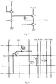
- the gate driving circuit consists of a plurality of cascaded shift registers, wherein each shift register is composed of at least four switching transistors T1, T2, T3, and T4, and a circuit structure diagram thereof is shown in Fig. 2 .
- an organic electroluminescence display panel comprises: a base substrate 100; a plurality of pixel driving circuits 200 and a gate driving circuit 300 disposed in the display area A of the base substrate 100; and a plurality of top emission type of light-emitting units 400 disposed in the display area A of the base substrate 100 and covering the plurality of pixel driving circuits 200 and the gate driving circuit 300.
- an orthographic projection of the gate driving circuit 300 on the base substrate 100 does not overlap with an orthographic projection of the plurality of pixel driving circuits 200 on the base substrate 100.
- the orthographic projection of the gate driving circuit 300 on the base substrate 100 at least partially overlaps with an orthographic projection of the plurality of top emission type of light-emitting units 400 on the base substrate 100.
- the gate driving circuit 300 and the pixel driving circuits 200 are simultaneously disposed in the display area A of the base substrate 100, and also it is ensured that the orthographic projection of the gate driving circuit 300 on the base substrate 100 does not overlap with the orthographic projection of the pixel driving circuits 200 on the base substrate 100. That is, the switching transistors in the gate driving circuit 300 are not disposed inside the pixel driving circuit 200 as in Fig. 3 , and thus will not occupy the wiring space of the pixel driving circuit 200. Therefore, it is ensured that both of the gate driving circuit 300 and the pixel driving circuit 200 have sufficient wiring spaces in the display area.
- a plurality of top emission type of light-emitting units 400 which is covering the pixel driving circuits 200 and the gate driving circuit 300, are further disposed in the display area A of the base substrate 100.
- the area occupied by each of the top emission type of light-emitting units is increased as compared with the conventional pixel unit (corresponding to the top emission type of light-emitting unit 400).
- one of the top emission type of light-emitting units 400 only overlaps with one of the pixel driving circuits 200.
- the conventional top emission type of light-emitting unit 400 is disposed in a region defined by the gate line and the data line.
- the gate driving circuit 300 has an overlapping region with the top emission type of light-emitting units 400 in the display area A. That is, according to an embodiment of the present disclosure, the top emission type of light-emitting units 400 may span over the data lines, thereby ensuring that all circuits in the display area A are covered by the top emission type of light-emitting units 400.
- both of the gate driving circuit 300 and the pixel driving circuits 200 have sufficient wiring spaces in the display area A, thereby eliminating the need for arranging the gate driving circuit 300 at the frame, and thus realizing an ultra-narrow frame or even a frameless design.
- each of the top emission type of light-emitting units 400 comprises generally an anode, a light-emitting layer, and a cathode that are sequentially stacked, wherein the anode is connected to a respective pixel driving circuit 200.
- the cathode is made of light transmissive material.
- the anode may be generally fabricated by an opaque metal, or a reflective layer can be fabricated separately under a transparent anode.
- the top emission type of light-emitting unit 400 may further comprise a functional film layer, such as an electron transport layer, a hole transport layer, an electron blocking layer, and a hole blocking layer, and the present disclosure is not limited in this regard.
- anodes of each of the top emission type of light-emitting units 400 may be distributed uniformly in the display area A of the base substrate 100. That is, intervals between anodes of the top emission type of light-emitting units 400 keep the same.
- anodes of the top emission type of light-emitting units 400 can be configured to be the same in shape and size.
- the light-emitting efficiency may be different depending on the material of the light-emitting layer in each of the top emission type of light-emitting units 400.
- the area occupied by the light-emitting layer and the anode in each of the top emission type of light-emitting units 400 based on the light-emitting efficiency. That is, the area occupied by the top emission type of light-emitting unit 400 having high light-emitting efficiency is relatively small, and the area occupied by the top emission type of light-emitting unit 400 having low light-emitting efficiency is relatively large.
- each of the top emission type of light-emitting units 400 is corresponding to a respective one of the pixel driving circuits 200, so as to drive the top emission type of light-emitting units 400 in a better way to emit light. That is, one pixel driving circuit 200 drives one of the top emission type of light-emitting units 400 to emit light. It is of course not excluded that one pixel driving circuit 200 drives a plurality of top emission type of light-emitting units 400 to emit light.
- the top emission type of light-emitting unit 400 since the area occupied by the top emission type of light-emitting unit 400 is increased, there may be a case where the top emission type of light-emitting unit 400 and its respective pixel driving circuit 200 do not directly overlap with each other. That is, for example, referring to Fig. 4 , the top emission type of light-emitting units 400 in the leftmost column has an overlapping region only with the gate driving circuit 300. In view of above, as shown in Figs. 4-6 , anodes of each of the top emission type of light-emitting units 400 need to be connected to their respective pixel driving circuits 200 by respective connection lines 500.
- connection lines 500 may be disposed in an existing conductive film layer, for example, disposed in the same layer as the gate lines, so as to reduce process steps. However, this will increase the complexity for wiring in the film.
- the connection lines 500 can be provided as a separate film layer.
- Fig. 7 which is a schematic diagram showing a hierarchical relationship between a connection line 500, a top emission type of light-emitting unit 400, and a pixel driving circuit 200 in an organic electroluminescence display panel according to an embodiment of the present disclosure.
- connection line 500 may be disposed between a first film layer 400' where the top emission type of light-emitting unit 400 is located and a second film layer 200' where the pixel driving circuit 200 is located.
- the film layers to be patterned in the fabricating process of the organic electroluminescence display panel are respectively: active layer ⁇ gate insulating layer ⁇ gate metal layer ⁇ interlayer insulating layer ⁇ source-drain metal layer ⁇ planarization layer ⁇ anode ⁇ pixel defining layer ⁇ spacer layer.
- two additional film layers are needed in the fabricating process.
- the film layers will change to be respectively: active layer ⁇ gate insulating layer ⁇ gate metal layer ⁇ interlayer insulating layer ⁇ source-drain metal layer ⁇ insulating layer ⁇ connection line layer ⁇ planarization layer ⁇ anode ⁇ pixel defining layer ⁇ spacer layer.
- the specific position for the gate driving circuit 300 in the display area A of the base substrate 100 is not limited, which may be determined based on the actual size of the display panel.
- the gate driving circuit 300 may be disposed at an edge of the display area A of the base substrate 100.
- the gate driving circuit 300 may comprise two gate sub-driving circuits, which are respectively disposed at two opposite edges of the display area of the base substrate 100, so as to achieve bilateral driving. In this way, problems such as signal delay in a large-sized panel can be alleviated.
- the gate driving circuit 300 may be disposed only at any edge of the display area A.
- the gate driving circuit 300 may be disposed at a position between two adjacent pixel driving circuits 200.
- the gate driving circuit 300 is disposed at an intermediate position of the display area A. Therefore, driving signals can be supplied at the same time to the gate lines at both sides, thereby contributing to a reduction of signal delay.
- the above content is merely for illustrating how to dispose the gate driving circuit 300 in the display area A of the above organic electroluminescence display panel provided by embodiments of the present disclosure, and the present disclosure is not limited thereto.
- a plurality of gate sub-driving circuits may be simultaneously disposed at edge and intermediate position of the display area A, and they constitute together the gate driving circuit 300.
- the present disclosure is in no way limited in this respect.
- embodiments of the present disclosure also provide a display device, comprising the organic electroluminescence display panel according to any of the above embodiments of the present disclosure.
- the display device can be any products or components having a display function, such as a mobile phone, a tablet computer, a television set, a display, a notebook computer, a digital photo frame, a navigator, and the like.
- a display function such as a mobile phone, a tablet computer, a television set, a display, a notebook computer, a digital photo frame, a navigator, and the like.
- embodiments of the present disclosure also provide a fabricating method for the above organic electroluminescence display panel.
- the fabricating method comprises the steps of: fabricating a gate driving circuit and a plurality of pixel driving circuits in a display area of a base substrate, wherein an orthogonal projection of the gate driving circuit on the base substrate does not overlap with an orthogonal projection of the plurality of pixel driving circuits on the base substrate; and fabricating further a plurality of top emission type of light-emitting units in the display area of the base substrate, wherein the plurality of top emission type of light-emitting units at least partially cover the plurality of pixel driving circuits and the gate driving circuit, and an orthographic projection of the gate driving circuit on the base substrate at least partially overlaps with an orthographic projection of the plurality of top emission type of light-emitting units on the base substrate.
- the above fabricating method provided by embodiments of the present disclosure may also comprise the following optional steps: after fabricating the gate driving circuit and the plurality of pixel driving circuits in the display area of the base substrate, and before fabricating further the plurality of top emission type of light-emitting units in the display area of the base substrate, fabricating connection lines for connecting an anode of each of the top emission type of light-emitting units to a respective pixel driving circuit.
- the film layers to be patterned are respectively: active layer ⁇ gate insulating layer ⁇ gate metal layer ⁇ interlayer insulating layer ⁇ source-drain metal layer ⁇ insulating layer ⁇ connection line layer ⁇ planarization layer ⁇ anode ⁇ pixel defining layer ⁇ spacer layer.
- active layer ⁇ gate insulating layer ⁇ gate metal layer ⁇ interlayer insulating layer ⁇ source-drain metal layer ⁇ insulating layer ⁇ connection line layer ⁇ planarization layer ⁇ anode ⁇ pixel defining layer ⁇ spacer layer.
- a driving circuit is constituted by a top gate transistor.
- the driving circuit can also be fabricated by a bottom gate transistor, which is not limited herein.
- Embodiments of the present disclosure provide an organic electroluminescence display panel, a fabricating method thereof, and a display device.
- the gate driving circuit and the pixel driving circuits are simultaneously disposed in the display area of the base substrate. Further, it is also ensured that the orthographic projection of the gate driving circuit on the base substrate does not overlap with the orthographic projection of the pixel driving circuits on the base substrate, thereby providing sufficient wiring spaces for both of the gate driving circuit and the pixel driving circuits in the display area. Further, a plurality of top emission type of light-emitting units at least partially covering the pixel driving circuits and the gate driving circuit are further provided in the display area of the base substrate.
- the gate driving circuit in the display area has an overlapping region with the top emission type of light-emitting units, thereby ensuring that all circuits in the display area are covered by the top emission type of light-emitting units. In this way, it is ensured that there are sufficient wiring spaces for the gate driving circuit and the pixel driving circuits in the display area, thereby eliminating the need to provide the gate driving circuit at the frame, and achieving an ultra-narrow frame or even a frameless design.
- orthographic projection of A on a base substrate refers to a projection of A onto the base substrate in a direction perpendicular to the base substrate, which should be readily appreciated by those skilled in the art.
Landscapes
- Engineering & Computer Science (AREA)
- Physics & Mathematics (AREA)
- Computer Hardware Design (AREA)
- General Physics & Mathematics (AREA)
- Theoretical Computer Science (AREA)
- Microelectronics & Electronic Packaging (AREA)
- Geometry (AREA)
- Electroluminescent Light Sources (AREA)
- Devices For Indicating Variable Information By Combining Individual Elements (AREA)
Abstract
Description
- The present application claims the benefit of Chinese Patent Application No.
201710516966.4, filed on June 29, 2017 - The present disclosure relates to the field of display technology, and discloses specifically an organic electroluminescence display panel, a fabricating method thereof, and a display device.
- In a conventional display panel, the display area is generally located in the middle of panel, and the gate driving circuit is located near the frame of panel. In this way, adverse effects on the display area due to the gate driving circuit are avoided. However, such an arrangement of gate driving circuit at the frame tends to result in display panels and subsequent display products with wider frames.
- Therefore, with the increasing popularity of narrow frames and even frameless designs, it has been proposed to move the gate driving circuit from the frame area to the display area, for example, into the pixel area, so as to narrow down and even eliminate the frame. However, in a specific implementation, it is extremely difficult to dispose a gate driving circuit in the display. For OLED products, especially high-resolution OLED products, it is very difficult to dispose further the gate driving circuit in a limited display area, since the complicated pixel driving circuit has been disposed in the same display area.
- According to an aspect of the present disclosure, an embodiment provides an organic electroluminescence display panel. The organic electroluminescence display panel comprises: a base substrate having a display area; a gate driving circuit and a plurality of pixel driving circuits located in the display area; and a plurality of top emission type of light-emitting units located in the display area. Further, in the above organic electroluminescence display panel, an orthographic projection of the gate driving circuit on the base substrate at least partially overlaps with an orthographic projection of the plurality of top emission type of light-emitting units on the base substrate.
- According to a possible implementation, in the above organic electroluminescence display panel provided by an embodiment of the present disclosure, the orthogonal projection of the gate driving circuit on the base substrate does not overlap with an orthogonal projection of the plurality of pixel driving circuits on the base substrate.
- According to a possible implementation, in the above organic electroluminescence display panel provided by an embodiment of the present disclosure, each of the top emission type of light-emitting units comprises an anode, a light-emitting layer and a cathode that are sequentially stacked, wherein the anode is connected to a respective pixel driving circuit.
- According to a possible implementation, in the above organic electroluminescence display panel provided by an embodiment of the present disclosure, the anode of each of the top emission type of light-emitting units is connected to a respective pixel driving circuit by a connection line.
- According to a possible implementation, in the above organic electroluminescence display panel provided by an embodiment of the present disclosure, the connection line is located between a first film layer where the respective top emission type of light-emitting unit is located and a second film layer where the respective pixel driving circuit is located.
- According to a possible implementation, in the above organic electroluminescence display panel provided by an embodiment of the present disclosure, the gate driving circuit is located at an edge of the display area of the base substrate.
- According to a possible implementation, in the above organic electroluminescence display panel provided by an embodiment of the present disclosure, the gate driving circuit comprises a gate sub-driving circuit located at an edge of the display area of the base substrate. Alternatively, in other implementations, the gate driving circuit comprises a first gate sub-driving circuit and a second gate sub-driving circuit located respectively at two opposite edges of the display area of the base substrate.
- According to a possible implementation, in the above organic electroluminescence display panel provided by an embodiment of the present disclosure, the gate driving circuit is located between two adjacent pixel driving circuits.
- According to another aspect of the present disclosure, an embodiment further provides a display device, comprising the above organic electroluminescence display panel according to embodiments of the present disclosure.
- According to yet another aspect of the present disclosure, an embodiment further provides a fabricating method for the above organic electroluminescence display panel. The fabricating method comprises steps of: fabricating a gate driving circuit and a plurality of pixel driving circuits in a display area of a base substrate, wherein an orthogonal projection of the gate driving circuit on the base substrate does not overlap with an orthogonal projection of the plurality of pixel driving circuits on the base substrate; and fabricating further a plurality of top emission type of light-emitting units in the display area of the base substrate, wherein the plurality of top emission type of light-emitting units at least partially cover the plurality of pixel driving circuits and the gate driving circuit, and an orthographic projection of the gate driving circuit on the base substrate at least partially overlaps with an orthographic projection of the plurality of top emission type of light-emitting units on the substrate.
- According to a possible implementation, in an embodiment of the present disclosure, the fabricating method for the above organic electroluminescence display panel also comprises steps of: after fabricating the gate driving circuit and the plurality of pixel driving circuits in the display area of the base substrate, and before fabricating further the plurality of top emission type of light-emitting units in the display area of the base substrate, fabricating connection lines, wherein the connection lines are configured to connect respectively an anode of each of the top emission type of light-emitting units to a respective pixel driving circuit.
-
-
Fig. 1 is a schematic structural diagram of a display panel according to a conventional approach; -
Fig. 2 is a schematic diagram showing a circuit structure of a shift register in the display panel ofFig. 1 ; -
Fig. 3 is a schematic diagram showing a circuit structure of a shift register located in a display area according to another conventional approach; -
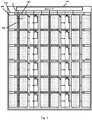
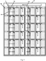
Figs. 4-6 are respectively schematic structural diagrams of organic electroluminescence display panels according to embodiments of the present disclosure; and -
Fig. 7 schematically shows a simplified cross-sectional view of a hierarchical relationship between a connection line, a top emission type of light-emitting unit, and a pixel driving circuit in an organic electroluminescence display panel according to an embodiment of the present disclosure. - Specific implementations of the organic electroluminescence display panel, the fabricating method thereof and the display device provided by embodiments of the present disclosure will be described in detail below with reference to the accompanying drawings.
- It should be noted that the thickness and shape of various film layers in the drawings do not represent any real proportion in the organic electroluminescence display panel, and are merely intended to illustrate the present disclosure.
- As shown in
Fig. 1 , according to a conventional approach, agate line 01, adata line 02, and apixel unit 03 are disposed in a display area A of a display panel, wherein the pixel unit is disposed in an area defined by thegate line 01 and thedata line 02. Also, a gate driving circuit for driving thegate line 01 is provided at the left and right frames. Specifically, the gate driving circuit consists of a plurality of cascaded shift registers, wherein each shift register is composed of at least four switching transistors T1, T2, T3, and T4, and a circuit structure diagram thereof is shown inFig. 2 . - As mentioned above, for the purpose of narrowing down the frame of display panel and even realizing a frameless design, it has been proposed to use the approach as shown in
Fig. 3 , in which the gate driving circuit that was located otherwise in the frame area is moved now to the pixel area. In this way, the space for disposing the gate driving circuit at the frame is eliminated, thereby realizing an ultra-narrow frame or even a frameless design. However, in actual operations, it is difficult to dispose a gate driving circuit in the display area. In particular, for OLED products, the difficulty is further increased, because in OLED products, especially in high-resolution OLED products, complex pixel circuits have already been disposed in the size-limited display area. - According to an embodiment of the present disclosure, an organic electroluminescence display panel is provided. As shown in
Figs. 4-6 , the organic electroluminescence display panel comprises: abase substrate 100; a plurality ofpixel driving circuits 200 and agate driving circuit 300 disposed in the display area A of thebase substrate 100; and a plurality of top emission type of light-emitting units 400 disposed in the display area A of thebase substrate 100 and covering the plurality ofpixel driving circuits 200 and thegate driving circuit 300. Further, an orthographic projection of thegate driving circuit 300 on thebase substrate 100 does not overlap with an orthographic projection of the plurality ofpixel driving circuits 200 on thebase substrate 100. Besides, the orthographic projection of thegate driving circuit 300 on thebase substrate 100 at least partially overlaps with an orthographic projection of the plurality of top emission type of light-emitting units 400 on thebase substrate 100. - Specifically, in the above organic electroluminescence display panel provided by an embodiment of the present disclosure, the
gate driving circuit 300 and thepixel driving circuits 200 are simultaneously disposed in the display area A of thebase substrate 100, and also it is ensured that the orthographic projection of thegate driving circuit 300 on thebase substrate 100 does not overlap with the orthographic projection of thepixel driving circuits 200 on thebase substrate 100. That is, the switching transistors in thegate driving circuit 300 are not disposed inside thepixel driving circuit 200 as inFig. 3 , and thus will not occupy the wiring space of thepixel driving circuit 200. Therefore, it is ensured that both of thegate driving circuit 300 and thepixel driving circuit 200 have sufficient wiring spaces in the display area. - Meanwhile, in the above organic electroluminescence display panel provided by an embodiment of the present disclosure, a plurality of top emission type of light-
emitting units 400, which is covering thepixel driving circuits 200 and thegate driving circuit 300, are further disposed in the display area A of thebase substrate 100. In such a case, according to an embodiment of the present disclosure, the area occupied by each of the top emission type of light-emitting units is increased as compared with the conventional pixel unit (corresponding to the top emission type of light-emitting unit 400). Specifically, in the conventional approach, one of the top emission type of light-emitting units 400 only overlaps with one of thepixel driving circuits 200. That is, the conventional top emission type of light-emitting unit 400 is disposed in a region defined by the gate line and the data line. However, according to an embodiment of the present disclosure, thegate driving circuit 300 has an overlapping region with the top emission type of light-emitting units 400 in the display area A. That is, according to an embodiment of the present disclosure, the top emission type of light-emitting units 400 may span over the data lines, thereby ensuring that all circuits in the display area A are covered by the top emission type of light-emitting units 400. In this way, it is ensured that both of thegate driving circuit 300 and thepixel driving circuits 200 have sufficient wiring spaces in the display area A, thereby eliminating the need for arranging thegate driving circuit 300 at the frame, and thus realizing an ultra-narrow frame or even a frameless design. - According to a specific embodiment, in the above organic electroluminescence display panel provided by an embodiment of the present disclosure, each of the top emission type of light-
emitting units 400 comprises generally an anode, a light-emitting layer, and a cathode that are sequentially stacked, wherein the anode is connected to a respectivepixel driving circuit 200. In order to ensure light emission from the cathode side of each of the top emission type of light-emitting units 400, it is required that the cathode is made of light transmissive material. However, the anode may be generally fabricated by an opaque metal, or a reflective layer can be fabricated separately under a transparent anode. In addition, the top emission type of light-emitting unit 400 may further comprise a functional film layer, such as an electron transport layer, a hole transport layer, an electron blocking layer, and a hole blocking layer, and the present disclosure is not limited in this regard. - According to a specific embodiment, in the above organic electroluminescence display panel provided by an embodiment of the present disclosure, in order to ensure that light-emitting regions are distributed uniformly in the display area A, as shown in
Figs. 4-6 , anodes of each of the top emission type of light-emitting units 400 may be distributed uniformly in the display area A of thebase substrate 100. That is, intervals between anodes of the top emission type of light-emitting units 400 keep the same. - According to a specific embodiment, in the above organic electroluminescence display panel provided by an embodiment of the present disclosure, in order to ensure that light-emitting regions are distributed uniformly in the display area A, as shown in
Figs. 4-6 , anodes of the top emission type of light-emitting units 400 can be configured to be the same in shape and size. Alternatively, when each of the top emission type of light-emitting units 400 is fabricated using a single color light-emitting layer, the light-emitting efficiency may be different depending on the material of the light-emitting layer in each of the top emission type of light-emittingunits 400. Therefore, in a specific embodiment, it is also possible to set the area occupied by the light-emitting layer and the anode in each of the top emission type of light-emitting units 400 based on the light-emitting efficiency. That is, the area occupied by the top emission type of light-emittingunit 400 having high light-emitting efficiency is relatively small, and the area occupied by the top emission type of light-emittingunit 400 having low light-emitting efficiency is relatively large. - According to a specific embodiment, in the above organic electroluminescence display panel provided by an embodiment of the present disclosure, advantageously, as shown in
Figs. 4-6 , each of the top emission type of light-emittingunits 400 is corresponding to a respective one of thepixel driving circuits 200, so as to drive the top emission type of light-emittingunits 400 in a better way to emit light. That is, onepixel driving circuit 200 drives one of the top emission type of light-emittingunits 400 to emit light. It is of course not excluded that onepixel driving circuit 200 drives a plurality of top emission type of light-emittingunits 400 to emit light. In this case, since the area occupied by the top emission type of light-emittingunit 400 is increased, there may be a case where the top emission type of light-emittingunit 400 and its respectivepixel driving circuit 200 do not directly overlap with each other. That is, for example, referring toFig. 4 , the top emission type of light-emittingunits 400 in the leftmost column has an overlapping region only with thegate driving circuit 300. In view of above, as shown inFigs. 4-6 , anodes of each of the top emission type of light-emittingunits 400 need to be connected to their respectivepixel driving circuits 200 by respective connection lines 500. - According to a specific embodiment, in the above organic electroluminescence display panel provided by an embodiment of the present disclosure, the
connection lines 500 may be disposed in an existing conductive film layer, for example, disposed in the same layer as the gate lines, so as to reduce process steps. However, this will increase the complexity for wiring in the film. In view of above, advantageously, in the above organic electroluminescence display panel provided by an embodiment of the present disclosure, theconnection lines 500 can be provided as a separate film layer. For example, referring toFig. 7 , which is a schematic diagram showing a hierarchical relationship between aconnection line 500, a top emission type of light-emittingunit 400, and apixel driving circuit 200 in an organic electroluminescence display panel according to an embodiment of the present disclosure. Specifically, theconnection line 500 may be disposed between a first film layer 400' where the top emission type of light-emittingunit 400 is located and a second film layer 200' where thepixel driving circuit 200 is located. This means that in the above embodiment, the film layers to be patterned in the fabricating process of the organic electroluminescence display panel are respectively: active layer→gate insulating layer→gate metal layer→interlayer insulating layer→source-drain metal layer→planarization layer→anode→pixel defining layer→spacer layer. In contrast, for the organic electroluminescence display panel provided by embodiments of the present disclosure, two additional film layers are needed in the fabricating process. That is, the film layers will change to be respectively: active layer→gate insulating layer→gate metal layer→interlayer insulating layer→source-drain metal layer→insulating layer→connection line layer→planarization layer→anode→pixel defining layer→spacer layer. - According to a specific embodiment, in the above organic electroluminescence display panel provided by an embodiment of the present disclosure, the specific position for the
gate driving circuit 300 in the display area A of thebase substrate 100 is not limited, which may be determined based on the actual size of the display panel. For example, as shown inFig. 4 , thegate driving circuit 300 may be disposed at an edge of the display area A of thebase substrate 100. Moreover, in the above organic electroluminescence display panel provided by an embodiment of the present disclosure, as shown inFig. 4 , thegate driving circuit 300 may comprise two gate sub-driving circuits, which are respectively disposed at two opposite edges of the display area of thebase substrate 100, so as to achieve bilateral driving. In this way, problems such as signal delay in a large-sized panel can be alleviated. Of course, alternatively, thegate driving circuit 300 may be disposed only at any edge of the display area A. - According to a specific embodiment, in the above organic electroluminescence display panel provided by an embodiment of the present disclosure, as shown in
Fig. 5 , thegate driving circuit 300 may be disposed at a position between two adjacentpixel driving circuits 200. For example, inFig. 5 , thegate driving circuit 300 is disposed at an intermediate position of the display area A. Therefore, driving signals can be supplied at the same time to the gate lines at both sides, thereby contributing to a reduction of signal delay. - Obviously, the above content is merely for illustrating how to dispose the
gate driving circuit 300 in the display area A of the above organic electroluminescence display panel provided by embodiments of the present disclosure, and the present disclosure is not limited thereto. For example, as shown inFig. 6 , a plurality of gate sub-driving circuits may be simultaneously disposed at edge and intermediate position of the display area A, and they constitute together thegate driving circuit 300. Of course, the present disclosure is in no way limited in this respect. - Based on the same concept, embodiments of the present disclosure also provide a display device, comprising the organic electroluminescence display panel according to any of the above embodiments of the present disclosure. The display device can be any products or components having a display function, such as a mobile phone, a tablet computer, a television set, a display, a notebook computer, a digital photo frame, a navigator, and the like. For specific implementations of the display device, reference may be made to the embodiments of the above organic electroluminescence display panel, and the repeated description is omitted herein.
- Based on the same concept, embodiments of the present disclosure also provide a fabricating method for the above organic electroluminescence display panel. The fabricating method comprises the steps of: fabricating a gate driving circuit and a plurality of pixel driving circuits in a display area of a base substrate, wherein an orthogonal projection of the gate driving circuit on the base substrate does not overlap with an orthogonal projection of the plurality of pixel driving circuits on the base substrate; and fabricating further a plurality of top emission type of light-emitting units in the display area of the base substrate, wherein the plurality of top emission type of light-emitting units at least partially cover the plurality of pixel driving circuits and the gate driving circuit, and an orthographic projection of the gate driving circuit on the base substrate at least partially overlaps with an orthographic projection of the plurality of top emission type of light-emitting units on the base substrate.
- According to a specific embodiment, the above fabricating method provided by embodiments of the present disclosure may also comprise the following optional steps: after fabricating the gate driving circuit and the plurality of pixel driving circuits in the display area of the base substrate, and before fabricating further the plurality of top emission type of light-emitting units in the display area of the base substrate, fabricating connection lines for connecting an anode of each of the top emission type of light-emitting units to a respective pixel driving circuit.
- For example, in the fabricating method for the organic electroluminescence display panel provided by embodiments of the present disclosure, the film layers to be patterned are respectively: active layer→gate insulating layer→gate metal layer→interlayer insulating layer→source-drain metal layer →insulating layer→connection line layer→planarization layer→anode→pixel defining layer→spacer layer. The above is merely an example in which a driving circuit is constituted by a top gate transistor. Of course, according to a specific embodiment, the driving circuit can also be fabricated by a bottom gate transistor, which is not limited herein.
- Embodiments of the present disclosure provide an organic electroluminescence display panel, a fabricating method thereof, and a display device. Specifically, in the above organic electroluminescence display panel, the gate driving circuit and the pixel driving circuits are simultaneously disposed in the display area of the base substrate. Further, it is also ensured that the orthographic projection of the gate driving circuit on the base substrate does not overlap with the orthographic projection of the pixel driving circuits on the base substrate, thereby providing sufficient wiring spaces for both of the gate driving circuit and the pixel driving circuits in the display area. Further, a plurality of top emission type of light-emitting units at least partially covering the pixel driving circuits and the gate driving circuit are further provided in the display area of the base substrate. Therefore, the area occupied by each of the top emission type of light-emitting units is increased. Those skilled in the art should readily contemplate that in a conventional display panel, one of the top emission type of light-emitting units overlaps only with one of the pixel driving circuits. However, by contrast, in embodiments of the present disclosure, the gate driving circuit in the display area has an overlapping region with the top emission type of light-emitting units, thereby ensuring that all circuits in the display area are covered by the top emission type of light-emitting units. In this way, it is ensured that there are sufficient wiring spaces for the gate driving circuit and the pixel driving circuits in the display area, thereby eliminating the need to provide the gate driving circuit at the frame, and achieving an ultra-narrow frame or even a frameless design.
- In all the descriptions herein, the expression of "orthographic projection of A on a base substrate" refers to a projection of A onto the base substrate in a direction perpendicular to the base substrate, which should be readily appreciated by those skilled in the art.
- Apparently, the person skilled in the art may make various alterations and variations to the present disclosure without departing the spirit and scope of the present disclosure. As such, provided that these modifications and variations of the present disclosure pertain to the scope of the claims of the present disclosure and their equivalents, the present disclosure is intended to embrace these alterations and variations.
Claims (12)
- An organic electroluminescence display panel, comprising:a base substrate having a display area;a gate driving circuit and a plurality of pixel driving circuits located in the display area; anda plurality of top emission type of light-emitting units located in the display area, whereinan orthographic projection of the gate driving circuit on the base substrate at least partially overlaps with an orthographic projection of the plurality of top emission type of light-emitting units on the base substrate.
- The organic electroluminescence display panel according to claim 1, wherein
the orthogonal projection of the gate driving circuit on the base substrate does not overlap with an orthogonal projection of the plurality of pixel driving circuits on the base substrate. - The organic electroluminescence display panel according to claim 1, wherein
the gate driving circuit is located at an edge of the display area. - The organic electroluminescence display panel according to claim 1, wherein
the gate driving circuit comprises a gate sub-driving circuit located at an edge of the display area. - The organic electroluminescence display panel according to claim 1, wherein
the gate driving circuit comprises a first gate sub-driving circuit and a second gate sub-driving circuit located respectively at two opposite edges of the display area. - The organic electroluminescence display panel according to claim 1, wherein
the gate driving circuit is located between two adjacent pixel driving circuits. - The organic electroluminescence display panel according to claim 1, wherein
each of the top emission type of light-emitting units comprises an anode, a light-emitting layer and a cathode that are sequentially stacked, wherein the anode is connected to a respective pixel driving circuits. - The organic electroluminescence display panel according to claim 7, wherein
the anode of each of the top emission type of light-emitting units is connected to the respective pixel driving circuits by a connection line. - The organic electroluminescence display panel according to claim 8, wherein
the connection line is located between a first film layer where the respective top emission type of light-emitting unit is located and a second film layer where the respective pixel driving circuit is located. - A display device comprising the organic electroluminescence display panel according to any of claims 1-9.
- A fabricating method for the organic electroluminescence display panel according to any of claims 1-9, comprising:fabricating a gate driving circuit and a plurality of pixel driving circuits in a display area of a base substrate, wherein an orthogonal projection of the gate driving circuit on the base substrate does not overlap with an orthogonal projection of the plurality of pixel driving circuits on the base substrate; andfabricating further a plurality of top emission type of light-emitting units in the display area, wherein the plurality of top emission type of light-emitting units at least partially cover the plurality of pixel driving circuits and the gate driving circuit, and the orthographic projection of the gate driving circuit on the base substrate at least partially overlaps with an orthographic projection of the plurality of top emission type of light-emitting units on the base substrate.
- The fabricating method according to claim 11, further comprising:
after fabricating the gate driving circuit and the plurality of pixel driving circuits in the display area of the base substrate, and before fabricating further the plurality of top emission type of light-emitting units in the display area, fabricating connection lines, wherein the connection lines are configured to connect respectively an anode of each of the top emission type of light-emitting units to a respective pixel driving circuit.
Priority Applications (1)
| Application Number | Priority Date | Filing Date | Title |
|---|---|---|---|
| EP24150369.7A EP4345809A3 (en) | 2017-06-29 | 2018-05-23 | Organic electroluminescence display panel, fabricating method thereof, and display device |
Applications Claiming Priority (2)
| Application Number | Priority Date | Filing Date | Title |
|---|---|---|---|
| CN201710516966.4A CN109192751A (en) | 2017-06-29 | 2017-06-29 | An organic electroluminescence display panel, its manufacturing method and display device |
| PCT/CN2018/087965 WO2019001177A1 (en) | 2017-06-29 | 2018-05-23 | Organic electroluminescent display panel and manufacturing method therefor, and display device |
Related Child Applications (2)
| Application Number | Title | Priority Date | Filing Date |
|---|---|---|---|
| EP24150369.7A Division EP4345809A3 (en) | 2017-06-29 | 2018-05-23 | Organic electroluminescence display panel, fabricating method thereof, and display device |
| EP24150369.7A Division-Into EP4345809A3 (en) | 2017-06-29 | 2018-05-23 | Organic electroluminescence display panel, fabricating method thereof, and display device |
Publications (3)
| Publication Number | Publication Date |
|---|---|
| EP3648168A1 true EP3648168A1 (en) | 2020-05-06 |
| EP3648168A4 EP3648168A4 (en) | 2021-03-31 |
| EP3648168B1 EP3648168B1 (en) | 2024-03-20 |
Family
ID=64740339
Family Applications (2)
| Application Number | Title | Priority Date | Filing Date |
|---|---|---|---|
| EP18825345.4A Active EP3648168B1 (en) | 2017-06-29 | 2018-05-23 | Organic electroluminescent display panel and manufacturing method therefor, and display device |
| EP24150369.7A Pending EP4345809A3 (en) | 2017-06-29 | 2018-05-23 | Organic electroluminescence display panel, fabricating method thereof, and display device |
Family Applications After (1)
| Application Number | Title | Priority Date | Filing Date |
|---|---|---|---|
| EP24150369.7A Pending EP4345809A3 (en) | 2017-06-29 | 2018-05-23 | Organic electroluminescence display panel, fabricating method thereof, and display device |
Country Status (4)
| Country | Link |
|---|---|
| US (2) | US20200111859A1 (en) |
| EP (2) | EP3648168B1 (en) |
| CN (2) | CN115425052A (en) |
| WO (1) | WO2019001177A1 (en) |
Families Citing this family (20)
| Publication number | Priority date | Publication date | Assignee | Title |
|---|---|---|---|---|
| CN115425052A (en) * | 2017-06-29 | 2022-12-02 | 京东方科技集团股份有限公司 | Display panel and display device |
| CN109671742B (en) * | 2018-12-06 | 2022-04-05 | 武汉华星光电半导体显示技术有限公司 | AMOLED display panel |
| CN111430415B (en) * | 2020-03-31 | 2023-01-10 | 合肥京东方卓印科技有限公司 | Display panel and display device |
| CN111261094A (en) | 2020-03-31 | 2020-06-09 | 深圳市华星光电半导体显示技术有限公司 | Grid driving array type display panel |
| CN113724667B (en) * | 2020-04-10 | 2023-04-07 | 京东方科技集团股份有限公司 | Display substrate, manufacturing method thereof and display device |
| CN113939865B (en) * | 2020-04-28 | 2024-04-19 | 京东方科技集团股份有限公司 | Display substrate and display device |
| EP4044163B1 (en) * | 2020-06-18 | 2023-10-25 | BOE Technology Group Co., Ltd. | Display panel and display apparatus |
| EP4044168A4 (en) * | 2020-06-18 | 2023-03-15 | BOE Technology Group Co., Ltd. | DISPLAY PANEL AND METHOD OF MANUFACTURING THEREOF, AND DISPLAY DEVICE |
| CN111768700B (en) | 2020-06-22 | 2021-10-08 | 武汉华星光电半导体显示技术有限公司 | Display panel and display device |
| CN111752030B (en) | 2020-07-29 | 2023-09-19 | 京东方科技集团股份有限公司 | Display substrate, liquid crystal display panel and liquid crystal display device |
| WO2022133830A1 (en) * | 2020-12-23 | 2022-06-30 | 京东方科技集团股份有限公司 | Display panel and display apparatus |
| CN113013202B (en) * | 2021-02-09 | 2022-12-02 | 武汉天马微电子有限公司 | Display panel and display device |
| CN113327963B (en) * | 2021-05-27 | 2025-05-09 | 京东方科技集团股份有限公司 | Display panel, display device, and method for manufacturing display panel |
| CN113362770B (en) * | 2021-06-02 | 2022-10-28 | 合肥京东方卓印科技有限公司 | Display panel and display device |
| CN113920940A (en) * | 2021-10-29 | 2022-01-11 | Oppo广东移动通信有限公司 | Display module assembly, display screen assembly and electronic equipment |
| CN116033799A (en) * | 2022-10-28 | 2023-04-28 | 京东方科技集团股份有限公司 | Display panel, manufacturing method thereof, and display device |
| CN117496852B (en) * | 2023-01-31 | 2026-04-21 | 武汉华星光电技术有限公司 | Display panel and display device |
| JP2024110511A (en) * | 2023-02-03 | 2024-08-16 | シャープディスプレイテクノロジー株式会社 | Multi-screen display device and liquid crystal module for multi-screen display device |
| CN117525106B (en) * | 2023-05-31 | 2025-09-16 | Tcl华星光电技术有限公司 | Display panel |
| CN122073103A (en) * | 2024-11-20 | 2026-05-22 | 京东方科技集团股份有限公司 | Display panel and display device |
Family Cites Families (24)
| Publication number | Priority date | Publication date | Assignee | Title |
|---|---|---|---|---|
| JP4646951B2 (en) * | 2007-06-06 | 2011-03-09 | 株式会社半導体エネルギー研究所 | Display device with sensor |
| KR100884450B1 (en) * | 2007-11-08 | 2009-02-19 | 삼성모바일디스플레이주식회사 | Organic light emitting display |
| KR101142752B1 (en) * | 2010-04-13 | 2012-05-03 | 삼성모바일디스플레이주식회사 | Flat Panel Display Device |
| KR101862347B1 (en) * | 2011-02-01 | 2018-07-05 | 삼성디스플레이 주식회사 | Display and display set having the same |
| KR101275810B1 (en) * | 2012-01-20 | 2013-06-18 | 삼성디스플레이 주식회사 | Organic light emitting display device |
| KR101987094B1 (en) * | 2012-06-15 | 2019-10-01 | 삼성디스플레이 주식회사 | Display device and fabrication method thereof |
| CN102903732A (en) * | 2012-10-12 | 2013-01-30 | 深圳市华星光电技术有限公司 | Organic light emitting diode device and corresponding display device |
| KR101958010B1 (en) * | 2012-12-17 | 2019-03-14 | 엘지디스플레이 주식회사 | Super Ultra High Resolution Organic Light Emitting Diode Display |
| KR102033557B1 (en) * | 2013-05-28 | 2019-10-17 | 엘지디스플레이 주식회사 | Organic light emitting diode display |
| US10255863B2 (en) * | 2014-04-02 | 2019-04-09 | Samsung Display Co., Ltd. | Display panel having a first region, a second region, and a third region between the first and second regions and including a drive portion on the third region |
| US9336709B2 (en) * | 2014-04-25 | 2016-05-10 | Apple Inc. | Displays with overlapping light-emitting diodes and gate drivers |
| CN104537993B (en) * | 2014-12-29 | 2018-09-21 | 厦门天马微电子有限公司 | Organic light emitting display panel |
| CN104701352B (en) * | 2015-03-20 | 2017-06-30 | 京东方科技集团股份有限公司 | A kind of array base palte, display panel and display device |
| CN104867450B (en) * | 2015-06-05 | 2017-09-19 | 京东方科技集团股份有限公司 | Array base palte and preparation method thereof, display device |
| CN105047686B (en) * | 2015-06-30 | 2018-09-04 | 京东方科技集团股份有限公司 | Array substrate, display panel and display device |
| KR102552583B1 (en) * | 2015-07-22 | 2023-07-06 | 삼성디스플레이 주식회사 | Display device |
| KR102465379B1 (en) * | 2015-12-02 | 2022-11-10 | 삼성디스플레이 주식회사 | Display apparatus |
| CN105405865A (en) * | 2015-12-31 | 2016-03-16 | 昆山工研院新型平板显示技术中心有限公司 | AMOLED display screen and pixel arrangement method |
| JP2017167403A (en) * | 2016-03-17 | 2017-09-21 | 株式会社ジャパンディスプレイ | Display device |
| CN106097968A (en) * | 2016-08-26 | 2016-11-09 | 京东方科技集团股份有限公司 | Display floater and display device |
| US10714552B2 (en) * | 2016-09-05 | 2020-07-14 | Sharp Kabushiki Kaisha | Active matrix substrate having plurality of circuit thin film transistors and pixel thin film transistors |
| CN106782416B (en) * | 2017-03-02 | 2019-12-13 | 上海天马微电子有限公司 | Display panel and display device |
| CN115425052A (en) * | 2017-06-29 | 2022-12-02 | 京东方科技集团股份有限公司 | Display panel and display device |
| CN206947350U (en) * | 2017-06-29 | 2018-01-30 | 京东方科技集团股份有限公司 | A kind of organic EL display panel and display device |
-
2017
- 2017-06-29 CN CN202211102536.5A patent/CN115425052A/en active Pending
- 2017-06-29 CN CN201710516966.4A patent/CN109192751A/en active Pending
-
2018
- 2018-05-23 EP EP18825345.4A patent/EP3648168B1/en active Active
- 2018-05-23 EP EP24150369.7A patent/EP4345809A3/en active Pending
- 2018-05-23 WO PCT/CN2018/087965 patent/WO2019001177A1/en not_active Ceased
- 2018-05-23 US US16/621,203 patent/US20200111859A1/en not_active Abandoned
-
2022
- 2022-09-15 US US17/932,495 patent/US20230006028A1/en not_active Abandoned
Also Published As
| Publication number | Publication date |
|---|---|
| CN109192751A (en) | 2019-01-11 |
| EP4345809A3 (en) | 2024-05-22 |
| EP3648168A4 (en) | 2021-03-31 |
| EP3648168B1 (en) | 2024-03-20 |
| US20200111859A1 (en) | 2020-04-09 |
| WO2019001177A1 (en) | 2019-01-03 |
| CN115425052A (en) | 2022-12-02 |
| EP4345809A2 (en) | 2024-04-03 |
| US20230006028A1 (en) | 2023-01-05 |
Similar Documents
| Publication | Publication Date | Title |
|---|---|---|
| US20230006028A1 (en) | Organic electroluminescence display panel, fabricating method thereof, and display device | |
| KR102443121B1 (en) | Display panel, manufacturing method thereof, and display device | |
| JP7331259B2 (en) | Display panel and display device | |
| CN110890026B (en) | Display panel and display device | |
| US10580836B2 (en) | OLED touch display panel with baffles on a TFT back plate, method for manufacturing the same and touch display device | |
| EP4053904B1 (en) | Display substrate and manufacturing method therefor, and display device | |
| CN206947350U (en) | A kind of organic EL display panel and display device | |
| US10460656B2 (en) | Display panel and display device | |
| EP4068260B1 (en) | Display substrate and display device | |
| CN109148537B (en) | Display panel, preparation method and electronic equipment | |
| CN207425860U (en) | A kind of organic electroluminescence display panel and display device | |
| US20170092698A1 (en) | An array substrate, display panel and display device | |
| CN109950293A (en) | A kind of display panel and display device | |
| CN115280504B (en) | Display substrate, display panel, and display device | |
| CN114930438B (en) | Display substrate, display panel and display device | |
| EP4488987A1 (en) | Display panel and display apparatus | |
| WO2022205858A1 (en) | Display panel and display apparatus | |
| US11387310B2 (en) | Array substrate with connection portion connecting power bus and power line and display panel | |
| CN113498534A (en) | Display substrate, driving method thereof and display device | |
| KR20230158123A (en) | Display panels and display devices | |
| CN120472834A (en) | Display substrate and display device | |
| US12484396B2 (en) | Array substrate and display device | |
| CN115413370A (en) | Display substrate and display device | |
| CN110164940B (en) | Organic light emitting display panel and display device | |
| US20200381494A1 (en) | Display panel and display device |
Legal Events
| Date | Code | Title | Description |
|---|---|---|---|
| STAA | Information on the status of an ep patent application or granted ep patent |
Free format text: STATUS: THE INTERNATIONAL PUBLICATION HAS BEEN MADE |
|
| PUAI | Public reference made under article 153(3) epc to a published international application that has entered the european phase |
Free format text: ORIGINAL CODE: 0009012 |
|
| STAA | Information on the status of an ep patent application or granted ep patent |
Free format text: STATUS: REQUEST FOR EXAMINATION WAS MADE |
|
| 17P | Request for examination filed |
Effective date: 20200122 |
|
| AK | Designated contracting states |
Kind code of ref document: A1 Designated state(s): AL AT BE BG CH CY CZ DE DK EE ES FI FR GB GR HR HU IE IS IT LI LT LU LV MC MK MT NL NO PL PT RO RS SE SI SK SM TR |
|
| AX | Request for extension of the european patent |
Extension state: BA ME |
|
| DAV | Request for validation of the european patent (deleted) | ||
| DAX | Request for extension of the european patent (deleted) | ||
| A4 | Supplementary search report drawn up and despatched |
Effective date: 20210302 |
|
| RIC1 | Information provided on ipc code assigned before grant |
Ipc: H01L 21/77 20170101ALI20210224BHEP Ipc: H01L 27/32 20060101AFI20210224BHEP Ipc: H01L 27/02 20060101ALI20210224BHEP Ipc: G09G 3/3225 20160101ALI20210224BHEP |
|
| REG | Reference to a national code |
Ref country code: DE Free format text: PREVIOUS MAIN CLASS: H01L0027320000 Ref country code: DE Ref legal event code: R079 Ref document number: 602018066942 Country of ref document: DE Free format text: PREVIOUS MAIN CLASS: H01L0027320000 Ipc: H10K0059121000 |
|
| GRAP | Despatch of communication of intention to grant a patent |
Free format text: ORIGINAL CODE: EPIDOSNIGR1 |
|
| STAA | Information on the status of an ep patent application or granted ep patent |
Free format text: STATUS: GRANT OF PATENT IS INTENDED |
|
| RIC1 | Information provided on ipc code assigned before grant |
Ipc: G09G 3/3266 20160101ALI20230925BHEP Ipc: H10K 59/131 20230101ALI20230925BHEP Ipc: G09G 3/3225 20160101ALI20230925BHEP Ipc: H01L 21/77 20170101ALI20230925BHEP Ipc: H01L 27/02 20060101ALI20230925BHEP Ipc: H10K 59/121 20230101AFI20230925BHEP |
|
| INTG | Intention to grant announced |
Effective date: 20231012 |
|
| GRAS | Grant fee paid |
Free format text: ORIGINAL CODE: EPIDOSNIGR3 |
|
| GRAA | (expected) grant |
Free format text: ORIGINAL CODE: 0009210 |
|
| STAA | Information on the status of an ep patent application or granted ep patent |
Free format text: STATUS: THE PATENT HAS BEEN GRANTED |
|
| AK | Designated contracting states |
Kind code of ref document: B1 Designated state(s): AL AT BE BG CH CY CZ DE DK EE ES FI FR GB GR HR HU IE IS IT LI LT LU LV MC MK MT NL NO PL PT RO RS SE SI SK SM TR |
|
| REG | Reference to a national code |
Ref country code: GB Ref legal event code: FG4D |
|
| REG | Reference to a national code |
Ref country code: CH Ref legal event code: EP |
|
| REG | Reference to a national code |
Ref country code: IE Ref legal event code: FG4D |
|
| REG | Reference to a national code |
Ref country code: DE Ref legal event code: R096 Ref document number: 602018066942 Country of ref document: DE |
|
| PG25 | Lapsed in a contracting state [announced via postgrant information from national office to epo] |
Ref country code: LT Free format text: LAPSE BECAUSE OF FAILURE TO SUBMIT A TRANSLATION OF THE DESCRIPTION OR TO PAY THE FEE WITHIN THE PRESCRIBED TIME-LIMIT Effective date: 20240320 |
|
| REG | Reference to a national code |
Ref country code: LT Ref legal event code: MG9D |
|
| PG25 | Lapsed in a contracting state [announced via postgrant information from national office to epo] |
Ref country code: GR Free format text: LAPSE BECAUSE OF FAILURE TO SUBMIT A TRANSLATION OF THE DESCRIPTION OR TO PAY THE FEE WITHIN THE PRESCRIBED TIME-LIMIT Effective date: 20240621 |
|
| PG25 | Lapsed in a contracting state [announced via postgrant information from national office to epo] |
Ref country code: HR Free format text: LAPSE BECAUSE OF FAILURE TO SUBMIT A TRANSLATION OF THE DESCRIPTION OR TO PAY THE FEE WITHIN THE PRESCRIBED TIME-LIMIT Effective date: 20240320 Ref country code: RS Free format text: LAPSE BECAUSE OF FAILURE TO SUBMIT A TRANSLATION OF THE DESCRIPTION OR TO PAY THE FEE WITHIN THE PRESCRIBED TIME-LIMIT Effective date: 20240620 |
|
| REG | Reference to a national code |
Ref country code: NL Ref legal event code: MP Effective date: 20240320 |
|
| PG25 | Lapsed in a contracting state [announced via postgrant information from national office to epo] |
Ref country code: RS Free format text: LAPSE BECAUSE OF FAILURE TO SUBMIT A TRANSLATION OF THE DESCRIPTION OR TO PAY THE FEE WITHIN THE PRESCRIBED TIME-LIMIT Effective date: 20240620 Ref country code: NO Free format text: LAPSE BECAUSE OF FAILURE TO SUBMIT A TRANSLATION OF THE DESCRIPTION OR TO PAY THE FEE WITHIN THE PRESCRIBED TIME-LIMIT Effective date: 20240620 Ref country code: LT Free format text: LAPSE BECAUSE OF FAILURE TO SUBMIT A TRANSLATION OF THE DESCRIPTION OR TO PAY THE FEE WITHIN THE PRESCRIBED TIME-LIMIT Effective date: 20240320 Ref country code: HR Free format text: LAPSE BECAUSE OF FAILURE TO SUBMIT A TRANSLATION OF THE DESCRIPTION OR TO PAY THE FEE WITHIN THE PRESCRIBED TIME-LIMIT Effective date: 20240320 Ref country code: GR Free format text: LAPSE BECAUSE OF FAILURE TO SUBMIT A TRANSLATION OF THE DESCRIPTION OR TO PAY THE FEE WITHIN THE PRESCRIBED TIME-LIMIT Effective date: 20240621 Ref country code: FI Free format text: LAPSE BECAUSE OF FAILURE TO SUBMIT A TRANSLATION OF THE DESCRIPTION OR TO PAY THE FEE WITHIN THE PRESCRIBED TIME-LIMIT Effective date: 20240320 Ref country code: BG Free format text: LAPSE BECAUSE OF FAILURE TO SUBMIT A TRANSLATION OF THE DESCRIPTION OR TO PAY THE FEE WITHIN THE PRESCRIBED TIME-LIMIT Effective date: 20240320 |
|
| REG | Reference to a national code |
Ref country code: AT Ref legal event code: MK05 Ref document number: 1668965 Country of ref document: AT Kind code of ref document: T Effective date: 20240320 |
|
| PG25 | Lapsed in a contracting state [announced via postgrant information from national office to epo] |
Ref country code: SE Free format text: LAPSE BECAUSE OF FAILURE TO SUBMIT A TRANSLATION OF THE DESCRIPTION OR TO PAY THE FEE WITHIN THE PRESCRIBED TIME-LIMIT Effective date: 20240320 Ref country code: LV Free format text: LAPSE BECAUSE OF FAILURE TO SUBMIT A TRANSLATION OF THE DESCRIPTION OR TO PAY THE FEE WITHIN THE PRESCRIBED TIME-LIMIT Effective date: 20240320 |
|
| PG25 | Lapsed in a contracting state [announced via postgrant information from national office to epo] |
Ref country code: NL Free format text: LAPSE BECAUSE OF FAILURE TO SUBMIT A TRANSLATION OF THE DESCRIPTION OR TO PAY THE FEE WITHIN THE PRESCRIBED TIME-LIMIT Effective date: 20240320 |
|
| PG25 | Lapsed in a contracting state [announced via postgrant information from national office to epo] |
Ref country code: NL Free format text: LAPSE BECAUSE OF FAILURE TO SUBMIT A TRANSLATION OF THE DESCRIPTION OR TO PAY THE FEE WITHIN THE PRESCRIBED TIME-LIMIT Effective date: 20240320 |
|
| PG25 | Lapsed in a contracting state [announced via postgrant information from national office to epo] |
Ref country code: IS Free format text: LAPSE BECAUSE OF FAILURE TO SUBMIT A TRANSLATION OF THE DESCRIPTION OR TO PAY THE FEE WITHIN THE PRESCRIBED TIME-LIMIT Effective date: 20240720 |
|
| PG25 | Lapsed in a contracting state [announced via postgrant information from national office to epo] |
Ref country code: PT Free format text: LAPSE BECAUSE OF FAILURE TO SUBMIT A TRANSLATION OF THE DESCRIPTION OR TO PAY THE FEE WITHIN THE PRESCRIBED TIME-LIMIT Effective date: 20240722 Ref country code: SM Free format text: LAPSE BECAUSE OF FAILURE TO SUBMIT A TRANSLATION OF THE DESCRIPTION OR TO PAY THE FEE WITHIN THE PRESCRIBED TIME-LIMIT Effective date: 20240320 |
|
| PG25 | Lapsed in a contracting state [announced via postgrant information from national office to epo] |
Ref country code: ES Free format text: LAPSE BECAUSE OF FAILURE TO SUBMIT A TRANSLATION OF THE DESCRIPTION OR TO PAY THE FEE WITHIN THE PRESCRIBED TIME-LIMIT Effective date: 20240320 |
|
| PG25 | Lapsed in a contracting state [announced via postgrant information from national office to epo] |
Ref country code: EE Free format text: LAPSE BECAUSE OF FAILURE TO SUBMIT A TRANSLATION OF THE DESCRIPTION OR TO PAY THE FEE WITHIN THE PRESCRIBED TIME-LIMIT Effective date: 20240320 Ref country code: CZ Free format text: LAPSE BECAUSE OF FAILURE TO SUBMIT A TRANSLATION OF THE DESCRIPTION OR TO PAY THE FEE WITHIN THE PRESCRIBED TIME-LIMIT Effective date: 20240320 |
|
| PG25 | Lapsed in a contracting state [announced via postgrant information from national office to epo] |
Ref country code: AT Free format text: LAPSE BECAUSE OF FAILURE TO SUBMIT A TRANSLATION OF THE DESCRIPTION OR TO PAY THE FEE WITHIN THE PRESCRIBED TIME-LIMIT Effective date: 20240320 |
|
| PG25 | Lapsed in a contracting state [announced via postgrant information from national office to epo] |
Ref country code: PL Free format text: LAPSE BECAUSE OF FAILURE TO SUBMIT A TRANSLATION OF THE DESCRIPTION OR TO PAY THE FEE WITHIN THE PRESCRIBED TIME-LIMIT Effective date: 20240320 |
|
| PG25 | Lapsed in a contracting state [announced via postgrant information from national office to epo] |
Ref country code: SK Free format text: LAPSE BECAUSE OF FAILURE TO SUBMIT A TRANSLATION OF THE DESCRIPTION OR TO PAY THE FEE WITHIN THE PRESCRIBED TIME-LIMIT Effective date: 20240320 |
|
| PG25 | Lapsed in a contracting state [announced via postgrant information from national office to epo] |
Ref country code: SM Free format text: LAPSE BECAUSE OF FAILURE TO SUBMIT A TRANSLATION OF THE DESCRIPTION OR TO PAY THE FEE WITHIN THE PRESCRIBED TIME-LIMIT Effective date: 20240320 Ref country code: SK Free format text: LAPSE BECAUSE OF FAILURE TO SUBMIT A TRANSLATION OF THE DESCRIPTION OR TO PAY THE FEE WITHIN THE PRESCRIBED TIME-LIMIT Effective date: 20240320 Ref country code: RO Free format text: LAPSE BECAUSE OF FAILURE TO SUBMIT A TRANSLATION OF THE DESCRIPTION OR TO PAY THE FEE WITHIN THE PRESCRIBED TIME-LIMIT Effective date: 20240320 Ref country code: PT Free format text: LAPSE BECAUSE OF FAILURE TO SUBMIT A TRANSLATION OF THE DESCRIPTION OR TO PAY THE FEE WITHIN THE PRESCRIBED TIME-LIMIT Effective date: 20240722 Ref country code: PL Free format text: LAPSE BECAUSE OF FAILURE TO SUBMIT A TRANSLATION OF THE DESCRIPTION OR TO PAY THE FEE WITHIN THE PRESCRIBED TIME-LIMIT Effective date: 20240320 Ref country code: IS Free format text: LAPSE BECAUSE OF FAILURE TO SUBMIT A TRANSLATION OF THE DESCRIPTION OR TO PAY THE FEE WITHIN THE PRESCRIBED TIME-LIMIT Effective date: 20240720 Ref country code: ES Free format text: LAPSE BECAUSE OF FAILURE TO SUBMIT A TRANSLATION OF THE DESCRIPTION OR TO PAY THE FEE WITHIN THE PRESCRIBED TIME-LIMIT Effective date: 20240320 Ref country code: EE Free format text: LAPSE BECAUSE OF FAILURE TO SUBMIT A TRANSLATION OF THE DESCRIPTION OR TO PAY THE FEE WITHIN THE PRESCRIBED TIME-LIMIT Effective date: 20240320 Ref country code: CZ Free format text: LAPSE BECAUSE OF FAILURE TO SUBMIT A TRANSLATION OF THE DESCRIPTION OR TO PAY THE FEE WITHIN THE PRESCRIBED TIME-LIMIT Effective date: 20240320 Ref country code: AT Free format text: LAPSE BECAUSE OF FAILURE TO SUBMIT A TRANSLATION OF THE DESCRIPTION OR TO PAY THE FEE WITHIN THE PRESCRIBED TIME-LIMIT Effective date: 20240320 |
|
| PG25 | Lapsed in a contracting state [announced via postgrant information from national office to epo] |
Ref country code: IT Free format text: LAPSE BECAUSE OF FAILURE TO SUBMIT A TRANSLATION OF THE DESCRIPTION OR TO PAY THE FEE WITHIN THE PRESCRIBED TIME-LIMIT Effective date: 20240320 |
|
| REG | Reference to a national code |
Ref country code: DE Ref legal event code: R097 Ref document number: 602018066942 Country of ref document: DE |
|
| REG | Reference to a national code |
Ref country code: CH Ref legal event code: PL |
|
| PG25 | Lapsed in a contracting state [announced via postgrant information from national office to epo] |
Ref country code: IT Free format text: LAPSE BECAUSE OF FAILURE TO SUBMIT A TRANSLATION OF THE DESCRIPTION OR TO PAY THE FEE WITHIN THE PRESCRIBED TIME-LIMIT Effective date: 20240320 |
|
| PG25 | Lapsed in a contracting state [announced via postgrant information from national office to epo] |
Ref country code: MC Free format text: LAPSE BECAUSE OF FAILURE TO SUBMIT A TRANSLATION OF THE DESCRIPTION OR TO PAY THE FEE WITHIN THE PRESCRIBED TIME-LIMIT Effective date: 20240320 |
|
| PG25 | Lapsed in a contracting state [announced via postgrant information from national office to epo] |
Ref country code: DK Free format text: LAPSE BECAUSE OF FAILURE TO SUBMIT A TRANSLATION OF THE DESCRIPTION OR TO PAY THE FEE WITHIN THE PRESCRIBED TIME-LIMIT Effective date: 20240320 |
|
| PG25 | Lapsed in a contracting state [announced via postgrant information from national office to epo] |
Ref country code: LU Free format text: LAPSE BECAUSE OF NON-PAYMENT OF DUE FEES Effective date: 20240523 |
|
| PLBE | No opposition filed within time limit |
Free format text: ORIGINAL CODE: 0009261 |
|
| STAA | Information on the status of an ep patent application or granted ep patent |
Free format text: STATUS: NO OPPOSITION FILED WITHIN TIME LIMIT |
|
| PG25 | Lapsed in a contracting state [announced via postgrant information from national office to epo] |
Ref country code: MC Free format text: LAPSE BECAUSE OF FAILURE TO SUBMIT A TRANSLATION OF THE DESCRIPTION OR TO PAY THE FEE WITHIN THE PRESCRIBED TIME-LIMIT Effective date: 20240320 Ref country code: LU Free format text: LAPSE BECAUSE OF NON-PAYMENT OF DUE FEES Effective date: 20240523 Ref country code: DK Free format text: LAPSE BECAUSE OF FAILURE TO SUBMIT A TRANSLATION OF THE DESCRIPTION OR TO PAY THE FEE WITHIN THE PRESCRIBED TIME-LIMIT Effective date: 20240320 Ref country code: CH Free format text: LAPSE BECAUSE OF NON-PAYMENT OF DUE FEES Effective date: 20240531 |
|
| REG | Reference to a national code |
Ref country code: BE Ref legal event code: MM Effective date: 20240531 |
|
| 26N | No opposition filed |
Effective date: 20241223 |
|
| GBPC | Gb: european patent ceased through non-payment of renewal fee |
Effective date: 20240620 |
|
| PG25 | Lapsed in a contracting state [announced via postgrant information from national office to epo] |
Ref country code: IE Free format text: LAPSE BECAUSE OF NON-PAYMENT OF DUE FEES Effective date: 20240523 |
|
| PG25 | Lapsed in a contracting state [announced via postgrant information from national office to epo] |
Ref country code: BE Free format text: LAPSE BECAUSE OF NON-PAYMENT OF DUE FEES Effective date: 20240531 Ref country code: SI Free format text: LAPSE BECAUSE OF FAILURE TO SUBMIT A TRANSLATION OF THE DESCRIPTION OR TO PAY THE FEE WITHIN THE PRESCRIBED TIME-LIMIT Effective date: 20240320 |
|
| PG25 | Lapsed in a contracting state [announced via postgrant information from national office to epo] |
Ref country code: FR Free format text: LAPSE BECAUSE OF NON-PAYMENT OF DUE FEES Effective date: 20240531 |
|
| PG25 | Lapsed in a contracting state [announced via postgrant information from national office to epo] |
Ref country code: GB Free format text: LAPSE BECAUSE OF NON-PAYMENT OF DUE FEES Effective date: 20240620 |
|
| PG25 | Lapsed in a contracting state [announced via postgrant information from national office to epo] |
Ref country code: CY Free format text: LAPSE BECAUSE OF FAILURE TO SUBMIT A TRANSLATION OF THE DESCRIPTION OR TO PAY THE FEE WITHIN THE PRESCRIBED TIME-LIMIT; INVALID AB INITIO Effective date: 20180523 |
|
| PG25 | Lapsed in a contracting state [announced via postgrant information from national office to epo] |
Ref country code: HU Free format text: LAPSE BECAUSE OF FAILURE TO SUBMIT A TRANSLATION OF THE DESCRIPTION OR TO PAY THE FEE WITHIN THE PRESCRIBED TIME-LIMIT; INVALID AB INITIO Effective date: 20180523 |
|
| PG25 | Lapsed in a contracting state [announced via postgrant information from national office to epo] |
Ref country code: TR Free format text: LAPSE BECAUSE OF FAILURE TO SUBMIT A TRANSLATION OF THE DESCRIPTION OR TO PAY THE FEE WITHIN THE PRESCRIBED TIME-LIMIT Effective date: 20240320 |
|
| PGFP | Annual fee paid to national office [announced via postgrant information from national office to epo] |
Ref country code: DE Payment date: 20260520 Year of fee payment: 9 |