EP3647918A1 - Input device - Google Patents
Input device Download PDFInfo
- Publication number
- EP3647918A1 EP3647918A1 EP18822650.0A EP18822650A EP3647918A1 EP 3647918 A1 EP3647918 A1 EP 3647918A1 EP 18822650 A EP18822650 A EP 18822650A EP 3647918 A1 EP3647918 A1 EP 3647918A1
- Authority
- EP
- European Patent Office
- Prior art keywords
- base member
- input device
- region
- layer
- sensing region
- Prior art date
- Legal status (The legal status is an assumption and is not a legal conclusion. Google has not performed a legal analysis and makes no representation as to the accuracy of the status listed.)
- Granted
Links
- 230000003287 optical effect Effects 0.000 claims abstract description 66
- 238000005304 joining Methods 0.000 claims abstract description 54
- 239000000758 substrate Substances 0.000 claims abstract description 39
- 239000010410 layer Substances 0.000 claims description 120
- 239000012790 adhesive layer Substances 0.000 claims description 6
- 230000002093 peripheral effect Effects 0.000 description 10
- 238000010521 absorption reaction Methods 0.000 description 8
- 230000000052 comparative effect Effects 0.000 description 7
- 239000000853 adhesive Substances 0.000 description 6
- 230000001070 adhesive effect Effects 0.000 description 6
- 238000013459 approach Methods 0.000 description 6
- 239000010408 film Substances 0.000 description 6
- 239000011347 resin Substances 0.000 description 6
- 229920005989 resin Polymers 0.000 description 6
- 238000001514 detection method Methods 0.000 description 5
- 229920000089 Cyclic olefin copolymer Polymers 0.000 description 4
- 239000004840 adhesive resin Substances 0.000 description 4
- 229920006223 adhesive resin Polymers 0.000 description 4
- 239000000872 buffer Substances 0.000 description 4
- 229920005668 polycarbonate resin Polymers 0.000 description 4
- 239000004431 polycarbonate resin Substances 0.000 description 4
- 229920000139 polyethylene terephthalate Polymers 0.000 description 4
- 239000005020 polyethylene terephthalate Substances 0.000 description 4
- 230000000694 effects Effects 0.000 description 3
- 238000004519 manufacturing process Methods 0.000 description 3
- 238000000034 method Methods 0.000 description 3
- 239000004925 Acrylic resin Substances 0.000 description 2
- 229920000178 Acrylic resin Polymers 0.000 description 2
- 239000004642 Polyimide Substances 0.000 description 2
- 239000000470 constituent Substances 0.000 description 2
- 229920001577 copolymer Polymers 0.000 description 2
- 230000007423 decrease Effects 0.000 description 2
- 239000004973 liquid crystal related substance Substances 0.000 description 2
- 239000000463 material Substances 0.000 description 2
- -1 polyethylene terephthalate Polymers 0.000 description 2
- 229920001721 polyimide Polymers 0.000 description 2
- 238000004904 shortening Methods 0.000 description 2
- XOLBLPGZBRYERU-UHFFFAOYSA-N tin dioxide Chemical compound O=[Sn]=O XOLBLPGZBRYERU-UHFFFAOYSA-N 0.000 description 2
- 239000004020 conductor Substances 0.000 description 1
- 239000013039 cover film Substances 0.000 description 1
- 238000012217 deletion Methods 0.000 description 1
- 230000037430 deletion Effects 0.000 description 1
- 239000011521 glass Substances 0.000 description 1
- AMGQUBHHOARCQH-UHFFFAOYSA-N indium;oxotin Chemical compound [In].[Sn]=O AMGQUBHHOARCQH-UHFFFAOYSA-N 0.000 description 1
- 239000012464 large buffer Substances 0.000 description 1
- 239000007769 metal material Substances 0.000 description 1
- 239000002086 nanomaterial Substances 0.000 description 1
- 239000004033 plastic Substances 0.000 description 1
- 229920003023 plastic Polymers 0.000 description 1
- 230000002265 prevention Effects 0.000 description 1
- 238000002834 transmittance Methods 0.000 description 1
Images


Classifications
-
- H—ELECTRICITY
- H05—ELECTRIC TECHNIQUES NOT OTHERWISE PROVIDED FOR
- H05K—PRINTED CIRCUITS; CASINGS OR CONSTRUCTIONAL DETAILS OF ELECTRIC APPARATUS; MANUFACTURE OF ASSEMBLAGES OF ELECTRICAL COMPONENTS
- H05K3/00—Apparatus or processes for manufacturing printed circuits
- H05K3/36—Assembling printed circuits with other printed circuits
- H05K3/361—Assembling flexible printed circuits with other printed circuits
-
- G—PHYSICS
- G06—COMPUTING; CALCULATING OR COUNTING
- G06F—ELECTRIC DIGITAL DATA PROCESSING
- G06F3/00—Input arrangements for transferring data to be processed into a form capable of being handled by the computer; Output arrangements for transferring data from processing unit to output unit, e.g. interface arrangements
- G06F3/01—Input arrangements or combined input and output arrangements for interaction between user and computer
- G06F3/03—Arrangements for converting the position or the displacement of a member into a coded form
- G06F3/041—Digitisers, e.g. for touch screens or touch pads, characterised by the transducing means
- G06F3/044—Digitisers, e.g. for touch screens or touch pads, characterised by the transducing means by capacitive means
-
- G—PHYSICS
- G06—COMPUTING; CALCULATING OR COUNTING
- G06F—ELECTRIC DIGITAL DATA PROCESSING
- G06F1/00—Details not covered by groups G06F3/00 - G06F13/00 and G06F21/00
- G06F1/16—Constructional details or arrangements
- G06F1/1613—Constructional details or arrangements for portable computers
- G06F1/1633—Constructional details or arrangements of portable computers not specific to the type of enclosures covered by groups G06F1/1615 - G06F1/1626
- G06F1/1637—Details related to the display arrangement, including those related to the mounting of the display in the housing
- G06F1/1643—Details related to the display arrangement, including those related to the mounting of the display in the housing the display being associated to a digitizer, e.g. laptops that can be used as penpads
-
- G—PHYSICS
- G06—COMPUTING; CALCULATING OR COUNTING
- G06F—ELECTRIC DIGITAL DATA PROCESSING
- G06F3/00—Input arrangements for transferring data to be processed into a form capable of being handled by the computer; Output arrangements for transferring data from processing unit to output unit, e.g. interface arrangements
- G06F3/01—Input arrangements or combined input and output arrangements for interaction between user and computer
- G06F3/03—Arrangements for converting the position or the displacement of a member into a coded form
- G06F3/041—Digitisers, e.g. for touch screens or touch pads, characterised by the transducing means
- G06F3/0416—Control or interface arrangements specially adapted for digitisers
- G06F3/04164—Connections between sensors and controllers, e.g. routing lines between electrodes and connection pads
-
- G—PHYSICS
- G06—COMPUTING; CALCULATING OR COUNTING
- G06F—ELECTRIC DIGITAL DATA PROCESSING
- G06F3/00—Input arrangements for transferring data to be processed into a form capable of being handled by the computer; Output arrangements for transferring data from processing unit to output unit, e.g. interface arrangements
- G06F3/01—Input arrangements or combined input and output arrangements for interaction between user and computer
- G06F3/03—Arrangements for converting the position or the displacement of a member into a coded form
- G06F3/041—Digitisers, e.g. for touch screens or touch pads, characterised by the transducing means
- G06F3/047—Digitisers, e.g. for touch screens or touch pads, characterised by the transducing means using sets of wires, e.g. crossed wires
-
- H—ELECTRICITY
- H05—ELECTRIC TECHNIQUES NOT OTHERWISE PROVIDED FOR
- H05K—PRINTED CIRCUITS; CASINGS OR CONSTRUCTIONAL DETAILS OF ELECTRIC APPARATUS; MANUFACTURE OF ASSEMBLAGES OF ELECTRICAL COMPONENTS
- H05K1/00—Printed circuits
- H05K1/02—Details
- H05K1/11—Printed elements for providing electric connections to or between printed circuits
- H05K1/118—Printed elements for providing electric connections to or between printed circuits specially for flexible printed circuits, e.g. using folded portions
-
- H—ELECTRICITY
- H05—ELECTRIC TECHNIQUES NOT OTHERWISE PROVIDED FOR
- H05K—PRINTED CIRCUITS; CASINGS OR CONSTRUCTIONAL DETAILS OF ELECTRIC APPARATUS; MANUFACTURE OF ASSEMBLAGES OF ELECTRICAL COMPONENTS
- H05K1/00—Printed circuits
- H05K1/02—Details
- H05K1/14—Structural association of two or more printed circuits
- H05K1/147—Structural association of two or more printed circuits at least one of the printed circuits being bent or folded, e.g. by using a flexible printed circuit
-
- H—ELECTRICITY
- H05—ELECTRIC TECHNIQUES NOT OTHERWISE PROVIDED FOR
- H05K—PRINTED CIRCUITS; CASINGS OR CONSTRUCTIONAL DETAILS OF ELECTRIC APPARATUS; MANUFACTURE OF ASSEMBLAGES OF ELECTRICAL COMPONENTS
- H05K3/00—Apparatus or processes for manufacturing printed circuits
- H05K3/30—Assembling printed circuits with electric components, e.g. with resistor
- H05K3/32—Assembling printed circuits with electric components, e.g. with resistor electrically connecting electric components or wires to printed circuits
- H05K3/321—Assembling printed circuits with electric components, e.g. with resistor electrically connecting electric components or wires to printed circuits by conductive adhesives
- H05K3/323—Assembling printed circuits with electric components, e.g. with resistor electrically connecting electric components or wires to printed circuits by conductive adhesives by applying an anisotropic conductive adhesive layer over an array of pads
-
- G—PHYSICS
- G06—COMPUTING; CALCULATING OR COUNTING
- G06F—ELECTRIC DIGITAL DATA PROCESSING
- G06F2203/00—Indexing scheme relating to G06F3/00 - G06F3/048
- G06F2203/041—Indexing scheme relating to G06F3/041 - G06F3/045
- G06F2203/04102—Flexible digitiser, i.e. constructional details for allowing the whole digitising part of a device to be flexed or rolled like a sheet of paper
-
- G—PHYSICS
- G06—COMPUTING; CALCULATING OR COUNTING
- G06F—ELECTRIC DIGITAL DATA PROCESSING
- G06F2203/00—Indexing scheme relating to G06F3/00 - G06F3/048
- G06F2203/041—Indexing scheme relating to G06F3/041 - G06F3/045
- G06F2203/04103—Manufacturing, i.e. details related to manufacturing processes specially suited for touch sensitive devices
-
- G—PHYSICS
- G06—COMPUTING; CALCULATING OR COUNTING
- G06F—ELECTRIC DIGITAL DATA PROCESSING
- G06F3/00—Input arrangements for transferring data to be processed into a form capable of being handled by the computer; Output arrangements for transferring data from processing unit to output unit, e.g. interface arrangements
- G06F3/01—Input arrangements or combined input and output arrangements for interaction between user and computer
- G06F3/03—Arrangements for converting the position or the displacement of a member into a coded form
- G06F3/041—Digitisers, e.g. for touch screens or touch pads, characterised by the transducing means
- G06F3/044—Digitisers, e.g. for touch screens or touch pads, characterised by the transducing means by capacitive means
- G06F3/0446—Digitisers, e.g. for touch screens or touch pads, characterised by the transducing means by capacitive means using a grid-like structure of electrodes in at least two directions, e.g. using row and column electrodes
Definitions
- the present invention relates to an input device. More specifically, the present invention relates to an input device including a touch sensor that detects a position of approach of a finger or the like.
- a touch panel often used as an input device includes a touch sensor that detects a position of approach (hereinafter, approach encompasses contact) of a finger or the like to a detection region.
- a mutual capacitance touch panel is provided with a drive-side electrode and an output-side electrode.
- the drive-side electrode is given a drive pulse, and the output-side electrode detects a change in capacitance caused by approach of a finger or the like.
- a surface panel for clear display of an image and protection from contact of a finger or the like is provided on a topmost surface of the touch panel.
- the touch sensor is disposed between the surface panel and a display device such as a liquid crystal display device and is attached to the surface panel and the display device with use of a light-transmitting resin such as an optical clear adhesive (OCA).
- OCA optical clear adhesive
- an optical layer such as a polarizing film may be provided between the touch sensor and the surface panel.
- Patent Literature 1 discloses an integrated touch polarizing plate and a touch panel including the integrated touch polarizing plate.
- This touch panel includes an integrated touch polarizing plate including a first conductive film having a conductive layer on an upper surface thereof, a first adhesive layer provided on the conductive layer, and a polarizing plate provided on the first adhesive layer.
- Patent Literature 2 discloses an input device and a method for manufacturing the input device.
- This input device has a light-transmitting transparent base member, a transparent electrode layer that is provided in an input region on one surface of the transparent base member, and a draw-out electrode that is provided in a non-input region around the input region so as to be electrically connected to the transparent electrode layer.
- occurrence of an air bubble between a surface member and an optical adhesive layer is prevented by injecting a resin into a space between the transparent base member and the surface member that face each other.
- a wiring pattern extends to an edge part of a base member of a touch sensor so that conduction with a light-transmitting electrode of the touch sensor is obtained.
- the wiring pattern has a terminal part at an end thereof, and an electrode layer of a flexible substrate is connected to this terminal part.
- the optical layer is located on the connection region of the flexible substrate connected to the base member.
- this step is also referred to as a step of the optical layer.
- This step of the optical layer creates a space between the optical layer and the base member, and this space is observed as an air bubble. This air bubble interferes depending on an optical angle and deforms the optical layer by expanding in volume under a high-temperature environment. This can be a cause of poor appearance.
- An object of the present invention is to provide an input device in which a region where an air bubble created between a sensor unit and an optical layer is present can be narrowed.
- an input device includes a sensor unit having a support base member, a light-transmitting electrode unit that is provided in a sensing region on a first surface of the support base member, and a terminal part that is conductive with the light-transmitting electrode unit and is provided outside the sensing region on the first surface of the support base member; an optical layer that is superimposed on the sensor unit in a first direction; and a flexible wiring substrate having a connection region that is connected to the terminal part and is held between the optical layer and the support base member.
- the flexible wiring substrate has a flexible base member on which an electrode layer is provided and a wiring end that is an end of the electrode layer and is connected to the terminal part so as to be conductive with the terminal part with use of a conductive joining member in the connection region.
- the wiring end is located at a position set back from an end of the flexible base member on a sensing region side, so that the flexible base member has a protruding part on which the electrode layer is not stacked and that protrudes toward the sensing region side beyond the wiring end.
- the input device has, on the sensing region side relative to a front end of the protruding part, a part into which the conductive joining member does not stick out.
- a step of the optical layer can be absorbed from the protruding part of the flexible base member toward the sensing region side in the part into which the conductive joining member does not stick out. This makes it possible to narrow a length of a region where an air bubble formed by the step of the optical layer is present.
- the input device may be configured such that a height, from the first surface, of the conductive joining member that sticks out toward the sensing region side beyond the protruding part is equal to or lower than a height of the protruding part from the first surface. This makes it possible to absorb the step of the optical layer from the front end of the protruding part toward the sensing region side even in a case where a part of the conductive joining member protrudes beyond the protruding part of the flexible base member.
- the input device may be configured to further include a protection layer provided between the light-transmitting electrode unit and the optical layer, wherein an adhesive layer that fixes the protection layer and the optical layer is located so as to reach an end of an outer periphery of a main surface of the protection layer.
- a protection layer provided between the light-transmitting electrode unit and the optical layer, wherein an adhesive layer that fixes the protection layer and the optical layer is located so as to reach an end of an outer periphery of a main surface of the protection layer.
- the input device may be configured such that a ratio of a thickness of the protection layer to the height of the protruding part from the first surface is 0.2 or more.
- a larger thickness of the protection layer leads to a smaller step of the optical layer and is therefore more preferable. That is, only from the perspective of reduction of the step, the ratio closer to 1 is more preferable, and as a result, the larger thickness of the protection layer is more preferable.
- a too large thickness of the protection layer decreases flexibility of the input device (touch panel).
- the thickness of the protection layer is realistically approximately 15 ⁇ m at most and is preferably 10 ⁇ m or less.
- the input device may be configured such that the protruding part is provided so as to become closer to the support base member in a protruding direction.
- the protruding part is gradually lowered toward the front end thereof (toward the sensing region side), and therefore a start point of absorption of the step of the optical layer can be set on an outer side as compared with a case where the protruding part is not lowered.
- the input device may be configured such that the conductive joining member does not stick out toward the sensing region side beyond the front end of the protruding part when viewed in the first direction. With this configuration, a whole end of the flexible base member on the sensing region side is the protruding part, and it is therefore possible to effectively absorb the step of the optical layer.
- the input device may be configured to further have a decorative layer that covers a peripheral region located outside the sensing region when viewed in the first direction.
- a region where the decorative layer is provided is an invisible region, and a region on an inner side of the invisible region is a visible region.
- the input device may be configured such that a surface member (a surface panel) is provided on an operation surface (a surface which an operating body such as a finger approaches) side.
- an input device in which a region where an air bubble created between a sensor unit and an optical layer is present can be narrowed.
- Fig. 1 is an exploded perspective view illustrating an input device according to the present embodiment.
- Fig. 2 is a plan view schematically illustrating the input device according to the present embodiment. More specifically, Fig. 2 is a plan view schematically illustrating a connection part of a flexible wiring substrate 40 in the input device 1.
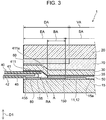
- Fig. 3 is a cross-sectional view schematically illustrating the input device according to the present embodiment. More specifically, Fig. 3 is a cross-sectional view schematically illustrating the connection part of the flexible wiring substrate 40 in the input device 1. For convenience of description, a display device 100 is not illustrated in Fig. 3 .
- the input device 1 includes a sensor unit 10 that is, for example, a capacitance type touch sensor, a surface panel (surface base member) 20 superimposed on the sensor unit 10 in a first direction D1, an optical layer 30 provided between the sensor unit 10 and the surface panel 20, and a flexible wiring substrate 40 connected to the sensor unit 10.
- the input device 1 is, for example, a touch panel.
- the input device 1 is attached onto the display device 100 such as a liquid crystal display device.
- the sensor unit 10 detects a position on the basis of a change in electrostatic capacitance caused by approach of a finger or the like to a detection region of a sensing region SA.
- the sensor unit 10 includes a support base member 15, and a first electrode 11 and a second electrode 12 that are light-transmitting electrode units provided in the sensing region SA on a first surface 15a of the support base member 15.
- the support base member 15 is, for example, made of a light-transmitting flexible film such as polyethylene terephthalate (PET), cycloolefin polymer (COP), or cycloolefin copolymer (COC) or a light-transmitting hard plate member such as an acrylic resin or a polycarbonate resin (PC).
- the first electrode 11 extends in one direction (e.g., an X direction) along a surface of the support base member 15, and the second electrode 12 extends in a direction (e.g., a Y direction) orthogonal to the one direction along the surface of the support base member 15.
- the first electrode 11 and the second electrode 12 are insulated from each other.
- a plurality of first electrodes 11 are disposed at predetermined intervals in the Y direction
- a plurality of second electrodes 12 are disposed at predetermined intervals in the X direction.
- the first electrode 11 and the second electrode 12 each have a plurality of island-shaped electrodes in the present embodiment.
- Each of the island-shaped electrodes has, for example, a shape close to a rhombus.
- the first electrode 11 and the second electrode 12 are provided so as to overlap the sensing region SA and therefore have light transmittance for transmitting an image displayed by the display device 100.
- the first electrode 11 and the second electrode 12 are made of a light-transmitting conductive material (e.g., indium tin oxide (ITO), SnO 2 , ZnO, a conductive nanomaterial, or a metal material formed in a net shape).
- a terminal part 155 is provided in a peripheral region EA on an outer side of the sensing region SA.
- a draw-out pattern 150 conductive with the first electrode 11 and the second electrode 12 extends in the peripheral region EA and is connected to the terminal part 155.
- the terminal part 155 is connected to a wiring end 455 in a connection region CA of the flexible wiring substrate 40.
- a protection layer 50 is provided on the first electrode 11, the second electrode 12, and the draw-out pattern 150.
- the protection layer 50 is a cover film and is provided between (i) the first electrode 11, the second electrode 12, and the draw-out pattern 150 and (ii) the optical layer 30.
- the surface panel 20 for protecting the sensor unit 10 is provided on the sensor unit 10 (on a side where the first electrode 11 and the second electrode 12 are provided).
- the surface panel 20 is a light-transmitting thin-plate-shaped member made of glass or plastic.
- the optical layer 30 provided between the sensor unit 10 and the surface panel 20 is, for example, a polarizing plate, a 1/4 ⁇ wave plate, or an optical adjustment base member in which the polarizing plate and the 1/4 ⁇ wave plate are stacked.
- the optical layer 30 has a film shape.
- the optical layer 30 is preferably made of the same material as the support base member 15 (a light-transmitting flexible film such as polyethylene terephthalate (PET), cycloolefin polymer (COP), or cycloolefin copolymer (COC) or a light-transmitting hard plate member such as an acrylic resin or a polycarbonate resin (PC)).
- PET polyethylene terephthalate
- COP cycloolefin polymer
- COC cycloolefin copolymer
- the optical layer 30 is attached onto the sensor unit 10 with use of an adhesive 35.
- connection region CA of the flexible wiring substrate 40 is held between, for example, an end of the optical layer 30 and the support base member 15. Since the connection region CA of the flexible wiring substrate 40 is held between the optical layer 30 and the support base member 15, load caused by application of stress onto the support base member 15 in a case where the flexible wiring substrate 40 is bent is lessened, and thereby breakage of the support base member 15 and peel of the flexible wiring substrate 40 are suppressed.
- connection region CA of the flexible wiring substrate 40 is held between the optical layer 30 and the support base member 15
- an end of the film-shaped optical layer 30 is fixed so as to be located on the flexible wiring substrate 40.
- the optical layer 30 is attached onto the sensor unit 10 so as to absorb a step created by a thickness of the flexible wiring substrate 40. This step creates a space (an air bubble region A) between the optical layer 30 and the sensor unit 10 on a sensing region SA side relative to an end of the flexible wiring substrate 40.
- the flexible wiring substrate 40 has a flexible base member 41 on which an electrode layer 45 is provided.
- the flexible base member 41 is a film base member having flexibility such as polyimide.
- the flexible wiring substrate 40 has a structure in which the electrode layer 45 is held between the flexible base member 41 on a front surface side and a flexible base member 42 on a rear surface side.
- the wiring end 455 is an end of the electrode layer 45.
- the wiring end 455 is not covered with the flexible base member 42 on the rear surface side.
- the wiring end 455 is connected to the terminal part 155 so as to be conductive with the terminal part 155 with use of a conductive joining member 80 in the connection region CA.
- the conductive joining member 80 is an anisotropic conductive adhesive. Conduction between the wiring end 455 and the terminal part 155 can be obtained by holding the conductive joining member 80 between the wiring end 455 of the flexible wiring substrate 40 and the terminal part 155 of the support base member 15 and joining these members by pressure while applying heat.
- An adhesive resin layer 70 is provided as an adhesive layer between the surface panel 20 and the optical layer 30.
- the adhesive resin layer 70 is made of a light-transmitting resin such as an optical clear adhesive (OCA).
- OCA optical clear adhesive
- a decorative layer 60 is provided on a surface panel 20 side of the optical layer 30.
- the decorative layer 60 is, for example, provided on a rear surface of the surface panel 20. Since the peripheral region EA on an outer side of the sensing region SA is covered with the decorative layer 60, the draw-out pattern 150 and the flexible wiring substrate 40 can be prevented from being viewed. As illustrated in Fig.
- an inner-side end of the decorative layer 60 may be provided on an inner side relative to an end of the peripheral region EA on a sensing region SA side from the perspective of more stably achieving invisibility of the draw-out pattern 150 provided in the peripheral region EA.
- a region where the decorative layer 60 is provided is an invisible region DA and a visible region VA is present on an inner side of the invisible region DA when viewed in the direction D1.
- a thickness of the flexible base member 41 is approximately 10 ⁇ m to 25 ⁇ m, preferably approximately 10 ⁇ m to 15 ⁇ m, a thickness of the electrode layer 45 is approximately 12
- the wiring end 455 is located at a position set back from the end of the flexible base member 41 on the sensing region SA side. Accordingly, the flexible base member 41 has a protruding part 411 on which the electrode layer 45 is not stacked and that protrudes toward the sensing region SA side relative to the wiring end 455. In the present embodiment, a part RA into which the conductive joining member 80 does not stick out is present on the sensing region SA side relative to a front end 411a of the protruding part 411.
- the presence of the part RA into which the conductive joining member 80 does not stick out makes it possible to effectively absorb the step of the optical layer 30 from the protruding part 411 of the flexible base member 41 toward the sensing region SA side.
- the adhesive resin layer 70 that fixes the protection layer 50 and the optical layer 30 is located so as to reach an end of an outer periphery of a main surface of the protection layer 50, and the end of the outer periphery of the main surface of the protection layer 50 serves as an end of the air bubble region A on the sensing region SA side.
- a length of the air bubble region A becomes narrow.
- Narrowing the width of the peripheral region EA also narrows the width of the invisible region DA and therefore can widen the visible region VA. This makes it easy to meet a demand for a narrower frame (narrowing the width of the invisible region DA and widening the visible region VA to a position close to an end of the input device 1).
- Fig. 4 is a plan view schematically illustrating a state of the part into which the conductive joining member does not stick out. More specifically, Fig. 4 is an enlarged plan view schematically illustrating a part where the wiring end 455 is provided.
- the conductive joining member 80 is held between the wiring end 455 and the terminal part 155, and conduction and adhesion are achieved by pressure joining while applying heat. In this pressure joining step, the conductive joining member 80 is squashed so as to spread.
- the conductive joining member 80 that spreads to the sensing region SA side enters a space between the protruding part 411 of the flexible base member 41 and the terminal part 155.
- This space (a region between the protruding part 411 and the terminal part 155) is a region that can accommodate the conductive joining member 80.
- the conductive joining member 80 enters not only between the wiring end 455 and the terminal part 155 but also this space. This can heighten connection strength of the flexible wiring substrate 40.
- a front end 80a of the spread conductive joining member 80 on the sensing region SA side does not stick out beyond the front end 411a of the protruding part 411 of the flexible base member 41 on the sensing region SA side. This creates the part RA into which the conductive joining member 80 does not stick out to the sensing region SA side beyond the front end 411a of the protruding part 411.
- the length of the air bubble region A can be narrowed. Narrowing the length of the air bubble region A can shorten a length for absorption of the step of the optical layer 30 and can widen the sensing region SA accordingly. As illustrated in Fig. 3 , a region having a predetermined length is provided between an outer-side end of the sensing region SA and an inner-side end of the air bubble region A. This region is a buffer region BA that prevent poor appearance resulting from an air bubble from affecting the sensing region SA even in a case where poor appearance occurs due to the air bubble. Narrowing the length of the air bubble region A can also narrow the length of the buffer region BA.
- Figs. 5(a) and 5(b) are cross-sectional views schematically illustrating another example.
- Fig. 5(a) is a cross-sectional view schematically illustrating the connection part of the flexible wiring substrate 40 in the input device 1.
- the display device 100 is not illustrated in Fig. 5(a).
- Fig. 5(b) is an enlarged cross-sectional view schematically illustrating the protruding part 411 and surroundings thereof.
- Fig. 6 is a plan view schematically illustrating another example of a state of the part into which the conductive joining member does not stick out. More specifically, Fig. 6 is an enlarged plan view schematically illustrating a part where the wiring end 455 is provided.
- the part RA is provided throughout an entire region of the flexible base member 41 in the width direction. Meanwhile, in the other example illustrated in Figs. 5 and 6 , the part RA is provided over a part of the flexible base member 41 in the width direction.
- the part RA into which the conductive joining member 80 does not stick out is preferably provided throughout the entire region of the flexible base member 41 in the width direction, but the effect of shortening the length of the air bubble region A can be obtained even in a case where the part RA is provided over a part of the flexible base member 41 in the width direction. In order to obtain the effect of shortening the length of the air bubble region A, it is only necessary that the part RA into which the conductive joining member 80 does not stick out be provided over approximately 80% or more of the flexible base member 41 in the width direction.
- a height h1 of a topmost position of a sticking-out part of the conductive joining member 80 from the first surface 15a is equal to or lower than a height h2 of an upper surface of the protruding part 411 from the first surface 15a.
- the part of the conductive joining member 80 that sticks out does not affect absorption of the step of the optical layer 30 and as a result it is possible to narrow the length of the air bubble region A in some cases as long as the height h1 of the part of the conductive joining member 80 that sticks out is lower than the height h2 of the upper surface of the protruding part 411.
- Fig. 7 is a cross-sectional view schematically illustrating the comparative example. More specifically, Fig. 7 is a cross-sectional view schematically illustrating a connection part of the flexible wiring substrate 40 in an input device 2 according to the comparative example. For convenience of description, the display device 100 is not illustrated in Fig. 7 .
- Fig. 8 is a plan view schematically illustrating an example of a state in which a conductive joining member sticks out in the comparative example. More specifically, Fig. 8 is an enlarged plan view schematically illustrating a part where the wiring end 455 is provided.
- the wiring end 455 of the flexible wiring substrate 40 is located at a position hardly set back from the end of the flexible base member 41 on the sensing region SA side. Accordingly, the electrode layer 45 is provided so as to reach the sensing region SA side of the flexible base member 41, and therefore the region between the flexible base member 41 and the terminal part 155 cannot fully accommodate the conductive joining member 80.
- the conductive joining member 80 that spreads toward the sensing region SA side sticks out toward the sensing region SA side beyond the flexible base member 41 in a process for holding the conductive joining member 80 between the wiring end 455 and the terminal part 155 and joining these members by pressure while applying heat. Since the conductive joining member 80 sticks out, the part of the conductive joining member 80 that sticks out presses the optical layer 30. This prolongs a range of absorption of the step of the optical layer 30. Since the step absorption range needs to be set long, the sensing region SA is compressed accordingly. This hinders widening of the sensing region SA.
- the range of absorption of the step of the optical layer 30 can be shortened, and the sensing region SA can be widened accordingly.
- Fig. 9 is a schematic cross-sectional view for explaining a thickness of the protection layer. More specifically, Fig. 9 is a cross-sectional view schematically illustrating the connection part of the flexible wiring substrate 40 in the input device 1. For convenience of description, the display device 100 is not illustrated in Fig. 9 .
- a size of the step created by the flexible wiring substrate 40 can be adjusted by the thickness of the protection layer 50.
- a ratio of a thickness t1 of the protection layer 50 to the height h2 of the upper surface of the protruding part 411 from the first surface 15a may be 0.2 or more.
- a larger thickness t1 of the protection layer 50 leads to a smaller step of the optical layer 30 and is therefore more preferable. That is, only from the perspective of reduction of the step, the ratio closer to 1 is more preferable, and as a result, the larger thickness t1 of the protection layer 50 is more preferable.
- a too large thickness of the protection layer 50 decreases flexibility of the input device 1.
- the thickness t1 of the protection layer 50 is realistically approximately 15 ⁇ m at most and is preferably 10 ⁇ m or less.
- Fig. 10 is a cross-sectional view schematically illustrating another example of the protruding part. More specifically, Fig. 10 is a cross-sectional view schematically illustrating the connection part of the flexible wiring substrate 40 in the input device 1. For convenience of description, the display device 100 is not illustrated in Fig. 10 .
- the protruding part 411 illustrated in Fig. 10 is provided so as to become closer to the support base member 15 side in a protruding direction.
- the flexible base member 41 is made of a resin material, such as polyimide, having flexibility.
- the electrode layer 45 and the flexible base member 42 on the rear side do not overlap the protruding part 411. Accordingly, the protruding part 411 can be provided so as to be gradually lowered toward a front end thereof (toward the sensing region SA side) due to flexibility of the flexible base member 41.
- a start point of absorption of the step of the optical layer 30 can be set on an outer side (a side away from the sensing region SA) as compared with a case where the protruding part 411 is not lowered. This makes it possible to further shorten the length of the air bubble region A. As a result, it is possible to widen the sensing region SA.
- the input device 1 in which the sensing region SA can be widened by narrowing the air bubble region A formed between the sensor unit 10 and the optical layer 30.
- the surface panel 20 is located so as to cover the optical layer 30 in the input device 1, this configuration is not restrictive.
- the surface panel 20 may be located on the support base member 15 side of the sensor unit 10.
- an input device may be configured not to have the decorative layer 60 and the surface panel 20.
- the input device includes the sensor unit 10, the optical layer 30 superimposed on the sensor unit 10, and the flexible wiring substrate 40 having the connection region CA held between the support base member 15 of the sensor unit 10 and the optical layer 30 and further includes the protection layer 50 on a side of the optical layer 30 that faces the sensor unit 10 as needed.
Landscapes
- Engineering & Computer Science (AREA)
- Theoretical Computer Science (AREA)
- General Engineering & Computer Science (AREA)
- Microelectronics & Electronic Packaging (AREA)
- Human Computer Interaction (AREA)
- Physics & Mathematics (AREA)
- General Physics & Mathematics (AREA)
- Manufacturing & Machinery (AREA)
- Computer Networks & Wireless Communication (AREA)
- Computer Hardware Design (AREA)
- Position Input By Displaying (AREA)
Abstract
Description
- The present invention relates to an input device. More specifically, the present invention relates to an input device including a touch sensor that detects a position of approach of a finger or the like.
- A touch panel often used as an input device includes a touch sensor that detects a position of approach (hereinafter, approach encompasses contact) of a finger or the like to a detection region. For example, a mutual capacitance touch panel is provided with a drive-side electrode and an output-side electrode. The drive-side electrode is given a drive pulse, and the output-side electrode detects a change in capacitance caused by approach of a finger or the like.
- A surface panel for clear display of an image and protection from contact of a finger or the like is provided on a topmost surface of the touch panel. The touch sensor is disposed between the surface panel and a display device such as a liquid crystal display device and is attached to the surface panel and the display device with use of a light-transmitting resin such as an optical clear adhesive (OCA). Furthermore, an optical layer such as a polarizing film may be provided between the touch sensor and the surface panel.
-
Patent Literature 1 discloses an integrated touch polarizing plate and a touch panel including the integrated touch polarizing plate. This touch panel includes an integrated touch polarizing plate including a first conductive film having a conductive layer on an upper surface thereof, a first adhesive layer provided on the conductive layer, and a polarizing plate provided on the first adhesive layer. -
Patent Literature 2 discloses an input device and a method for manufacturing the input device. This input device has a light-transmitting transparent base member, a transparent electrode layer that is provided in an input region on one surface of the transparent base member, and a draw-out electrode that is provided in a non-input region around the input region so as to be electrically connected to the transparent electrode layer. In the method for manufacturing the input device, occurrence of an air bubble between a surface member and an optical adhesive layer is prevented by injecting a resin into a space between the transparent base member and the surface member that face each other. -
- PTL 1: Japanese Unexamined Patent Application Publication No.
2011-081810 - PTL 2: Japanese Unexamined Patent Application Publication No.
2012-190087 - In an input device that is a touch panel, a wiring pattern extends to an edge part of a base member of a touch sensor so that conduction with a light-transmitting electrode of the touch sensor is obtained. The wiring pattern has a terminal part at an end thereof, and an electrode layer of a flexible substrate is connected to this terminal part.
- When such a flexible substrate is connected to the base member of the touch sensor, a connection region of the flexible substrate is held between the base member and an optical layer in some cases in order to obtain sufficient connection strength. In this case, the optical layer is located on the connection region of the flexible substrate connected to the base member. As a result, the optical layer has a step based on a thickness of the flexible substrate. Hereinafter, this step is also referred to as a step of the optical layer. This step of the optical layer creates a space between the optical layer and the base member, and this space is observed as an air bubble. This air bubble interferes depending on an optical angle and deforms the optical layer by expanding in volume under a high-temperature environment. This can be a cause of poor appearance.
- In order to prevent occurrence of this space (air bubble), a resin is injected into the space in some cases. However, this requires a step of injecting the resin, thereby inviting an increase in the number of manufacturing steps. In other cases, although poor appearance is present due to the air bubble, a buffer region is provided between a region where the air bubble is located and an end of a detection region so that the air bubble does not affect the detection region where the light-transmitting electrode is disposed. In such cases, however, a large buffer region is needed in a case where the region where the air bubble is located is large. It is therefore difficult to meet recent demands for narrowing of a width of a region (where a draw-out wire is disposed) around the detection region. In view of this, making the region where the air bubble is located as narrow as possible is one of the most preferable measures from a perspective of prevention or reduction of various problems resulting from the air bubble.
- An object of the present invention is to provide an input device in which a region where an air bubble created between a sensor unit and an optical layer is present can be narrowed.
- In order to solve the above problems, an input device according to an aspect of the present invention includes a sensor unit having a support base member, a light-transmitting electrode unit that is provided in a sensing region on a first surface of the support base member, and a terminal part that is conductive with the light-transmitting electrode unit and is provided outside the sensing region on the first surface of the support base member; an optical layer that is superimposed on the sensor unit in a first direction; and a flexible wiring substrate having a connection region that is connected to the terminal part and is held between the optical layer and the support base member.
- In this input device, the flexible wiring substrate has a flexible base member on which an electrode layer is provided and a wiring end that is an end of the electrode layer and is connected to the terminal part so as to be conductive with the terminal part with use of a conductive joining member in the connection region. The wiring end is located at a position set back from an end of the flexible base member on a sensing region side, so that the flexible base member has a protruding part on which the electrode layer is not stacked and that protrudes toward the sensing region side beyond the wiring end. The input device has, on the sensing region side relative to a front end of the protruding part, a part into which the conductive joining member does not stick out.
- According to this configuration, a step of the optical layer can be absorbed from the protruding part of the flexible base member toward the sensing region side in the part into which the conductive joining member does not stick out. This makes it possible to narrow a length of a region where an air bubble formed by the step of the optical layer is present.
- The input device may be configured such that a height, from the first surface, of the conductive joining member that sticks out toward the sensing region side beyond the protruding part is equal to or lower than a height of the protruding part from the first surface. This makes it possible to absorb the step of the optical layer from the front end of the protruding part toward the sensing region side even in a case where a part of the conductive joining member protrudes beyond the protruding part of the flexible base member.
- The input device may be configured to further include a protection layer provided between the light-transmitting electrode unit and the optical layer, wherein an adhesive layer that fixes the protection layer and the optical layer is located so as to reach an end of an outer periphery of a main surface of the protection layer. With this configuration, the air bubble is located on an outer side of the protection layer, and therefore a length of the air bubble region can be narrowed.
- The input device may be configured such that a ratio of a thickness of the protection layer to the height of the protruding part from the first surface is 0.2 or more. A larger thickness of the protection layer leads to a smaller step of the optical layer and is therefore more preferable. That is, only from the perspective of reduction of the step, the ratio closer to 1 is more preferable, and as a result, the larger thickness of the protection layer is more preferable. However, a too large thickness of the protection layer decreases flexibility of the input device (touch panel). In view of this, the thickness of the protection layer is realistically approximately 15 µm at most and is preferably 10 µm or less.
- The input device may be configured such that the protruding part is provided so as to become closer to the support base member in a protruding direction. With this configuration, the protruding part is gradually lowered toward the front end thereof (toward the sensing region side), and therefore a start point of absorption of the step of the optical layer can be set on an outer side as compared with a case where the protruding part is not lowered.
- The input device may be configured such that the conductive joining member does not stick out toward the sensing region side beyond the front end of the protruding part when viewed in the first direction. With this configuration, a whole end of the flexible base member on the sensing region side is the protruding part, and it is therefore possible to effectively absorb the step of the optical layer.
- The input device may be configured to further have a decorative layer that covers a peripheral region located outside the sensing region when viewed in the first direction. A region where the decorative layer is provided is an invisible region, and a region on an inner side of the invisible region is a visible region. The input device may be configured such that a surface member (a surface panel) is provided on an operation surface (a surface which an operating body such as a finger approaches) side.
- According to the present invention, it is possible to provide an input device in which a region where an air bubble created between a sensor unit and an optical layer is present can be narrowed.
-
- [
Fig. 1] Fig. 1 is an exploded perspective view illustrating an input device according to the present embodiment. - [
Fig. 2] Fig. 2 is a plan view schematically illustrating the input device according to the present embodiment. - [
Fig. 3] Fig. 3 is a cross-sectional view schematically illustrating the input device according to the present embodiment. - [
Fig. 4] Fig. 4 is a plan view schematically illustrating a state of a part into which a conductive joining member does not stick out. - [
Fig. 5] Figs. 5(a) and 5(b) are cross-sectional views schematically illustrating another example. - [
Fig. 6] Fig. 6 is a plan view schematically illustrating another example of a state of a part into which the conductive joining member does not stick out. - [
Fig. 7] Fig. 7 is a cross-sectional view schematically illustrating a comparative example. - [
Fig. 8] Fig. 8 is a plan view schematically illustrating a state in which the conductive joining member sticks out according to the comparative example. - [
Fig. 9] Fig. 9 is a schematic cross-sectional view for explaining a thickness of a protection layer. - [
Fig. 10] Fig. 10 is a cross-sectional view schematically illustrating another example of a protruding part. - An embodiment of the present invention is described below with reference to the drawings. In the following description, identical members are given identical reference signs, and description of members described once is omitted as appropriate.
-
Fig. 1 is an exploded perspective view illustrating an input device according to the present embodiment. -
Fig. 2 is a plan view schematically illustrating the input device according to the present embodiment. More specifically,Fig. 2 is a plan view schematically illustrating a connection part of aflexible wiring substrate 40 in theinput device 1. -
Fig. 3 is a cross-sectional view schematically illustrating the input device according to the present embodiment. More specifically,Fig. 3 is a cross-sectional view schematically illustrating the connection part of theflexible wiring substrate 40 in theinput device 1. For convenience of description, adisplay device 100 is not illustrated inFig. 3 . - As illustrated in
Fig. 1 , theinput device 1 according to the present embodiment includes asensor unit 10 that is, for example, a capacitance type touch sensor, a surface panel (surface base member) 20 superimposed on thesensor unit 10 in a first direction D1, anoptical layer 30 provided between thesensor unit 10 and thesurface panel 20, and aflexible wiring substrate 40 connected to thesensor unit 10. Theinput device 1 is, for example, a touch panel. Theinput device 1 is attached onto thedisplay device 100 such as a liquid crystal display device. - The
sensor unit 10 detects a position on the basis of a change in electrostatic capacitance caused by approach of a finger or the like to a detection region of a sensing region SA. Thesensor unit 10 includes asupport base member 15, and afirst electrode 11 and asecond electrode 12 that are light-transmitting electrode units provided in the sensing region SA on afirst surface 15a of thesupport base member 15. Thesupport base member 15 is, for example, made of a light-transmitting flexible film such as polyethylene terephthalate (PET), cycloolefin polymer (COP), or cycloolefin copolymer (COC) or a light-transmitting hard plate member such as an acrylic resin or a polycarbonate resin (PC). - The
first electrode 11 extends in one direction (e.g., an X direction) along a surface of thesupport base member 15, and thesecond electrode 12 extends in a direction (e.g., a Y direction) orthogonal to the one direction along the surface of thesupport base member 15. Thefirst electrode 11 and thesecond electrode 12 are insulated from each other. In the present embodiment, a plurality offirst electrodes 11 are disposed at predetermined intervals in the Y direction, and a plurality ofsecond electrodes 12 are disposed at predetermined intervals in the X direction. - Although there are various kinds of electrode patterns that constitute the
first electrode 11 and thesecond electrode 12, thefirst electrode 11 and thesecond electrode 12 each have a plurality of island-shaped electrodes in the present embodiment. Each of the island-shaped electrodes has, for example, a shape close to a rhombus. - The
first electrode 11 and thesecond electrode 12 are provided so as to overlap the sensing region SA and therefore have light transmittance for transmitting an image displayed by thedisplay device 100. For this reason, thefirst electrode 11 and thesecond electrode 12 are made of a light-transmitting conductive material (e.g., indium tin oxide (ITO), SnO2, ZnO, a conductive nanomaterial, or a metal material formed in a net shape). - On the
support base member 15, aterminal part 155 is provided in a peripheral region EA on an outer side of the sensing region SA. A draw-outpattern 150 conductive with thefirst electrode 11 and thesecond electrode 12 extends in the peripheral region EA and is connected to theterminal part 155. Theterminal part 155 is connected to awiring end 455 in a connection region CA of theflexible wiring substrate 40. - A
protection layer 50 is provided on thefirst electrode 11, thesecond electrode 12, and the draw-outpattern 150. Theprotection layer 50 is a cover film and is provided between (i) thefirst electrode 11, thesecond electrode 12, and the draw-outpattern 150 and (ii) theoptical layer 30. - The
surface panel 20 for protecting thesensor unit 10 is provided on the sensor unit 10 (on a side where thefirst electrode 11 and thesecond electrode 12 are provided). Thesurface panel 20 is a light-transmitting thin-plate-shaped member made of glass or plastic. - The
optical layer 30 provided between thesensor unit 10 and thesurface panel 20 is, for example, a polarizing plate, a 1/4λ wave plate, or an optical adjustment base member in which the polarizing plate and the 1/4λ wave plate are stacked. Theoptical layer 30 has a film shape. Theoptical layer 30 is preferably made of the same material as the support base member 15 (a light-transmitting flexible film such as polyethylene terephthalate (PET), cycloolefin polymer (COP), or cycloolefin copolymer (COC) or a light-transmitting hard plate member such as an acrylic resin or a polycarbonate resin (PC)). Theoptical layer 30 is attached onto thesensor unit 10 with use of an adhesive 35. - The connection region CA of the
flexible wiring substrate 40 is held between, for example, an end of theoptical layer 30 and thesupport base member 15. Since the connection region CA of theflexible wiring substrate 40 is held between theoptical layer 30 and thesupport base member 15, load caused by application of stress onto thesupport base member 15 in a case where theflexible wiring substrate 40 is bent is lessened, and thereby breakage of thesupport base member 15 and peel of theflexible wiring substrate 40 are suppressed. - According to the configuration in which the connection region CA of the
flexible wiring substrate 40 is held between theoptical layer 30 and thesupport base member 15, an end of the film-shapedoptical layer 30 is fixed so as to be located on theflexible wiring substrate 40. Theoptical layer 30 is attached onto thesensor unit 10 so as to absorb a step created by a thickness of theflexible wiring substrate 40. This step creates a space (an air bubble region A) between theoptical layer 30 and thesensor unit 10 on a sensing region SA side relative to an end of theflexible wiring substrate 40. - The
flexible wiring substrate 40 has aflexible base member 41 on which anelectrode layer 45 is provided. Theflexible base member 41 is a film base member having flexibility such as polyimide. Theflexible wiring substrate 40 has a structure in which theelectrode layer 45 is held between theflexible base member 41 on a front surface side and aflexible base member 42 on a rear surface side. - The
wiring end 455 is an end of theelectrode layer 45. Thewiring end 455 is not covered with theflexible base member 42 on the rear surface side. Thewiring end 455 is connected to theterminal part 155 so as to be conductive with theterminal part 155 with use of a conductive joiningmember 80 in the connection region CA. The conductive joiningmember 80 is an anisotropic conductive adhesive. Conduction between thewiring end 455 and theterminal part 155 can be obtained by holding the conductive joiningmember 80 between thewiring end 455 of theflexible wiring substrate 40 and theterminal part 155 of thesupport base member 15 and joining these members by pressure while applying heat. - An
adhesive resin layer 70 is provided as an adhesive layer between thesurface panel 20 and theoptical layer 30. Theadhesive resin layer 70 is made of a light-transmitting resin such as an optical clear adhesive (OCA). In the peripheral region EA, adecorative layer 60 is provided on asurface panel 20 side of theoptical layer 30. Thedecorative layer 60 is, for example, provided on a rear surface of thesurface panel 20. Since the peripheral region EA on an outer side of the sensing region SA is covered with thedecorative layer 60, the draw-outpattern 150 and theflexible wiring substrate 40 can be prevented from being viewed. As illustrated inFig. 3 , an inner-side end of thedecorative layer 60 may be provided on an inner side relative to an end of the peripheral region EA on a sensing region SA side from the perspective of more stably achieving invisibility of the draw-outpattern 150 provided in the peripheral region EA. In this case, as illustrated inFig. 3 , a region where thedecorative layer 60 is provided is an invisible region DA and a visible region VA is present on an inner side of the invisible region DA when viewed in the direction D1. - Thicknesses of the respective constituent elements are described below but are not limited to these. A thickness of the
flexible base member 41 is approximately 10 µm to 25 µm, preferably approximately 10 µm to 15 µm, a thickness of theelectrode layer 45 is approximately 12 |um to 25 µm, typically approximately 20 µm, a thickness of theflexible base member 42 is approximately 30 µm, a thickness of the conductive joiningmember 80 is approximately 3 µm to 10 µm, a thickness of theoptical layer 30 is approximately 150 µm, a thickness of the adhesive 35 is approximately 10 µm to 20 µm, and a thickness of theprotection layer 50 is approximately 5 µm to 15 µm. Accordingly, theoptical layer 30 is attached over a step of approximately 30 µm to 40 µm, and the air bubble region A is created in this step part. - In the
input device 1, thewiring end 455 is located at a position set back from the end of theflexible base member 41 on the sensing region SA side. Accordingly, theflexible base member 41 has aprotruding part 411 on which theelectrode layer 45 is not stacked and that protrudes toward the sensing region SA side relative to thewiring end 455. In the present embodiment, a part RA into which the conductive joiningmember 80 does not stick out is present on the sensing region SA side relative to afront end 411a of theprotruding part 411. - The presence of the part RA into which the conductive joining
member 80 does not stick out makes it possible to effectively absorb the step of theoptical layer 30 from the protrudingpart 411 of theflexible base member 41 toward the sensing region SA side. Specifically, theadhesive resin layer 70 that fixes theprotection layer 50 and theoptical layer 30 is located so as to reach an end of an outer periphery of a main surface of theprotection layer 50, and the end of the outer periphery of the main surface of theprotection layer 50 serves as an end of the air bubble region A on the sensing region SA side. - As a result, a length of the air bubble region A becomes narrow. This narrows a width of the peripheral region EA, thereby making it possible to widen the area of the sensing region SA. Narrowing the width of the peripheral region EA also narrows the width of the invisible region DA and therefore can widen the visible region VA. This makes it easy to meet a demand for a narrower frame (narrowing the width of the invisible region DA and widening the visible region VA to a position close to an end of the input device 1).
-
Fig. 4 is a plan view schematically illustrating a state of the part into which the conductive joining member does not stick out. More specifically,Fig. 4 is an enlarged plan view schematically illustrating a part where thewiring end 455 is provided. - In a case where the
flexible wiring substrate 40 is connected, the conductive joiningmember 80 is held between thewiring end 455 and theterminal part 155, and conduction and adhesion are achieved by pressure joining while applying heat. In this pressure joining step, the conductive joiningmember 80 is squashed so as to spread. - The conductive joining
member 80 that spreads to the sensing region SA side enters a space between theprotruding part 411 of theflexible base member 41 and theterminal part 155. This space (a region between theprotruding part 411 and the terminal part 155) is a region that can accommodate the conductive joiningmember 80. The conductive joiningmember 80 enters not only between thewiring end 455 and theterminal part 155 but also this space. This can heighten connection strength of theflexible wiring substrate 40. - Due to the presence of the region that can accommodate the conductive joining
member 80, afront end 80a of the spread conductive joiningmember 80 on the sensing region SA side does not stick out beyond thefront end 411a of theprotruding part 411 of theflexible base member 41 on the sensing region SA side. This creates the part RA into which the conductive joiningmember 80 does not stick out to the sensing region SA side beyond thefront end 411a of theprotruding part 411. - Since the conductive joining
member 80 does not stick out beyond thefront end 411a of theprotruding part 411, the length of the air bubble region A can be narrowed. Narrowing the length of the air bubble region A can shorten a length for absorption of the step of theoptical layer 30 and can widen the sensing region SA accordingly. As illustrated inFig. 3 , a region having a predetermined length is provided between an outer-side end of the sensing region SA and an inner-side end of the air bubble region A. This region is a buffer region BA that prevent poor appearance resulting from an air bubble from affecting the sensing region SA even in a case where poor appearance occurs due to the air bubble. Narrowing the length of the air bubble region A can also narrow the length of the buffer region BA. -
Figs. 5(a) and 5(b) are cross-sectional views schematically illustrating another example.Fig. 5(a) is a cross-sectional view schematically illustrating the connection part of theflexible wiring substrate 40 in theinput device 1. For convenience of description, thedisplay device 100 is not illustrated inFig. 5(a). Fig. 5(b) is an enlarged cross-sectional view schematically illustrating theprotruding part 411 and surroundings thereof. -
Fig. 6 is a plan view schematically illustrating another example of a state of the part into which the conductive joining member does not stick out. More specifically,Fig. 6 is an enlarged plan view schematically illustrating a part where thewiring end 455 is provided. - In the aforementioned state of the part RA into which the conductive joining
member 80 does not stick out, the part RA is provided throughout an entire region of theflexible base member 41 in the width direction. Meanwhile, in the other example illustrated inFigs. 5 and6 , the part RA is provided over a part of theflexible base member 41 in the width direction. - The part RA into which the conductive joining
member 80 does not stick out is preferably provided throughout the entire region of theflexible base member 41 in the width direction, but the effect of shortening the length of the air bubble region A can be obtained even in a case where the part RA is provided over a part of theflexible base member 41 in the width direction. In order to obtain the effect of shortening the length of the air bubble region A, it is only necessary that the part RA into which the conductive joiningmember 80 does not stick out be provided over approximately 80% or more of theflexible base member 41 in the width direction. - As illustrated in
Fig. 5(b) , even in a case where the conductive joiningmember 80 sticks out toward the sensing region SA side beyond the protrudingpart 411 in a part of theflexible base member 41 in the width direction, a height h1 of a topmost position of a sticking-out part of the conductive joiningmember 80 from thefirst surface 15a is equal to or lower than a height h2 of an upper surface of theprotruding part 411 from thefirst surface 15a. With this configuration, the part of the conductive joiningmember 80 that sticks out beyond the protrudingpart 411 of theflexible base member 41 does not make contact with theoptical layer 30 and does not hinder absorption of the step of theoptical layer 30. Even in a case where the conductive joiningmember 80 sticks out toward the sensing region SA side beyond the protrudingpart 411 throughout the entire region of theflexible base member 41, the part of the conductive joiningmember 80 that sticks out does not affect absorption of the step of theoptical layer 30 and as a result it is possible to narrow the length of the air bubble region A in some cases as long as the height h1 of the part of the conductive joiningmember 80 that sticks out is lower than the height h2 of the upper surface of theprotruding part 411. - A comparative example is described below.
-
Fig. 7 is a cross-sectional view schematically illustrating the comparative example. More specifically,Fig. 7 is a cross-sectional view schematically illustrating a connection part of theflexible wiring substrate 40 in aninput device 2 according to the comparative example. For convenience of description, thedisplay device 100 is not illustrated inFig. 7 . -
Fig. 8 is a plan view schematically illustrating an example of a state in which a conductive joining member sticks out in the comparative example. More specifically,Fig. 8 is an enlarged plan view schematically illustrating a part where thewiring end 455 is provided. - In the
input device 2 according to the comparative example, thewiring end 455 of theflexible wiring substrate 40 is located at a position hardly set back from the end of theflexible base member 41 on the sensing region SA side. Accordingly, theelectrode layer 45 is provided so as to reach the sensing region SA side of theflexible base member 41, and therefore the region between theflexible base member 41 and theterminal part 155 cannot fully accommodate the conductive joiningmember 80. - Therefore, when the
flexible wiring substrate 40 is connected, the conductive joiningmember 80 that spreads toward the sensing region SA side sticks out toward the sensing region SA side beyond theflexible base member 41 in a process for holding the conductive joiningmember 80 between thewiring end 455 and theterminal part 155 and joining these members by pressure while applying heat. Since the conductive joiningmember 80 sticks out, the part of the conductive joiningmember 80 that sticks out presses theoptical layer 30. This prolongs a range of absorption of the step of theoptical layer 30. Since the step absorption range needs to be set long, the sensing region SA is compressed accordingly. This hinders widening of the sensing region SA. - Meanwhile, in a case where the part RA into which the conductive joining
member 80 does not stick out toward the sensing region SA beyond thefront end 411a of theprotruding part 411 as in the present embodiment, the range of absorption of the step of theoptical layer 30 can be shortened, and the sensing region SA can be widened accordingly. -
Fig. 9 is a schematic cross-sectional view for explaining a thickness of the protection layer. More specifically,Fig. 9 is a cross-sectional view schematically illustrating the connection part of theflexible wiring substrate 40 in theinput device 1. For convenience of description, thedisplay device 100 is not illustrated inFig. 9 . - In the
input device 1, a size of the step created by theflexible wiring substrate 40 can be adjusted by the thickness of theprotection layer 50. For example, a ratio of a thickness t1 of theprotection layer 50 to the height h2 of the upper surface of theprotruding part 411 from thefirst surface 15a may be 0.2 or more. A larger thickness t1 of theprotection layer 50 leads to a smaller step of theoptical layer 30 and is therefore more preferable. That is, only from the perspective of reduction of the step, the ratio closer to 1 is more preferable, and as a result, the larger thickness t1 of theprotection layer 50 is more preferable. However, a too large thickness of theprotection layer 50 decreases flexibility of theinput device 1. In view of this, the thickness t1 of theprotection layer 50 is realistically approximately 15 µm at most and is preferably 10 µm or less. -
Fig. 10 is a cross-sectional view schematically illustrating another example of the protruding part. More specifically,Fig. 10 is a cross-sectional view schematically illustrating the connection part of theflexible wiring substrate 40 in theinput device 1. For convenience of description, thedisplay device 100 is not illustrated inFig. 10 . - The protruding
part 411 illustrated inFig. 10 is provided so as to become closer to thesupport base member 15 side in a protruding direction. Theflexible base member 41 is made of a resin material, such as polyimide, having flexibility. Theelectrode layer 45 and theflexible base member 42 on the rear side do not overlap theprotruding part 411. Accordingly, the protrudingpart 411 can be provided so as to be gradually lowered toward a front end thereof (toward the sensing region SA side) due to flexibility of theflexible base member 41. - In the case where the
protruding part 411 is gradually lowered toward the front end thereof, a start point of absorption of the step of theoptical layer 30 can be set on an outer side (a side away from the sensing region SA) as compared with a case where theprotruding part 411 is not lowered. This makes it possible to further shorten the length of the air bubble region A. As a result, it is possible to widen the sensing region SA. - As described above, according to the present embodiment, it is possible to provide the
input device 1 in which the sensing region SA can be widened by narrowing the air bubble region A formed between thesensor unit 10 and theoptical layer 30. - Although the present embodiment has been described above, the present invention is not limited to these examples. For example, appropriate addition, deletion, and design change of a constituent element in the above embodiment and an appropriate combination of features of the embodiment are also encompassed within the scope of the present invention without departing from the spirit of the present invention.
- For example, although the
surface panel 20 is located so as to cover theoptical layer 30 in theinput device 1, this configuration is not restrictive. Thesurface panel 20 may be located on thesupport base member 15 side of thesensor unit 10. - Although the
input device 1 is configured such that thedecorative layer 60 and thesurface panel 20 are superimposed on a multilayer body in which theflexible wiring substrate 40 is held between thesensor unit 10 and theoptical layer 30 in the above description, an input device according to an embodiment of the present invention may be configured not to have thedecorative layer 60 and thesurface panel 20. In this case, the input device includes thesensor unit 10, theoptical layer 30 superimposed on thesensor unit 10, and theflexible wiring substrate 40 having the connection region CA held between thesupport base member 15 of thesensor unit 10 and theoptical layer 30 and further includes theprotection layer 50 on a side of theoptical layer 30 that faces thesensor unit 10 as needed. -
- 1, 2 input device
- 10 sensor unit
- 11 first electrode
- 12 second electrode
- 15 support base member
- 15a first surface
- 20 surface panel
- 30 optical layer
- 35 adhesive
- 40 flexible wiring substrate
- 41, 42 flexible base member
- 45 electrode layer
- 50 protection layer
- 60 decorative layer
- 70 adhesive resin layer
- 80 conductive joining member
- 80a front end
- 100 display device
- 150 draw-out pattern
- 155 terminal part
- 411 protruding part
- 411a front end
- 455 wiring end
- A air bubble region
- BA buffer region
- CA connection region
- D1 first direction
- DA invisible region
- EA peripheral region
- RA part into which conductive joining member does not stick out
- SA sensing region
- VA visible region
- h1, h2 height
- t1 thickness
Claims (6)
- An input device comprising:a sensor unit having a support base member, a light-transmitting electrode unit that is provided in a sensing region on a first surface of the support base member, and a terminal part that is conductive with the light-transmitting electrode unit and is provided outside the sensing region on the first surface of the support base member;an optical layer that is superimposed on the sensor unit in a first direction; anda flexible wiring substrate having a connection region that is connected to the terminal part and is held between the optical layer and the support base member,whereinthe flexible wiring substrate has a flexible base member on which an electrode layer is provided and a wiring end that is an end of the electrode layer and is connected to the terminal part so as to be conductive with the terminal part with use of a conductive joining member in the connection region,the wiring end is located at a position set back from an end of the flexible base member on a sensing region side, so that the flexible base member has a protruding part on which the electrode layer is not stacked and that protrudes toward the sensing region side beyond the wiring end, anda part into which the conductive joining member does not stick out is present on the sensing region side relative to a front end of the protruding part.
- The input device according to Claim 1, wherein
a height, from the first surface, of the conductive joining member that sticks out toward the sensing region side beyond the protruding part is equal to or lower than a height of the protruding part from the first surface. - The input device according to Claim 1 or 2, further comprising a protection layer provided between the light-transmitting electrode unit and the optical layer,
wherein an adhesive layer that fixes the protection layer and the optical layer is located so as to reach an end of an outer periphery of a main surface of the protection layer. - The input device according to Claim 3, wherein
a ratio of a thickness of the protection layer to the height of the protruding part from the first surface is 0.2 or more. - The input device according to any one of Claims 1 through 4, wherein
the protruding part is provided so as to become closer to the support base member in a protruding direction. - The input device according to any one of Claims 1 through 5, wherein
the conductive joining member does not stick out toward the sensing region side beyond the front end of the protruding part when viewed in the first direction.
Applications Claiming Priority (2)
| Application Number | Priority Date | Filing Date | Title |
|---|---|---|---|
| JP2017127174 | 2017-06-29 | ||
| PCT/JP2018/019937 WO2019003732A1 (en) | 2017-06-29 | 2018-05-24 | Input device |
Publications (3)
| Publication Number | Publication Date |
|---|---|
| EP3647918A1 true EP3647918A1 (en) | 2020-05-06 |
| EP3647918A4 EP3647918A4 (en) | 2021-04-07 |
| EP3647918B1 EP3647918B1 (en) | 2022-04-20 |
Family
ID=64741304
Family Applications (1)
| Application Number | Title | Priority Date | Filing Date |
|---|---|---|---|
| EP18822650.0A Active EP3647918B1 (en) | 2017-06-29 | 2018-05-24 | Input device |
Country Status (7)
| Country | Link |
|---|---|
| US (1) | US11284520B2 (en) |
| EP (1) | EP3647918B1 (en) |
| JP (1) | JP6831913B2 (en) |
| KR (1) | KR102325850B1 (en) |
| CN (1) | CN110678829B (en) |
| TW (1) | TWI652606B (en) |
| WO (1) | WO2019003732A1 (en) |
Families Citing this family (2)
| Publication number | Priority date | Publication date | Assignee | Title |
|---|---|---|---|---|
| JP2019040407A (en) * | 2017-08-25 | 2019-03-14 | ホシデン株式会社 | Resin laminate and touch input device provided with the same |
| JP7444593B2 (en) * | 2019-12-13 | 2024-03-06 | シャープ株式会社 | Display device, display device manufacturing method, and printed wiring board |
Family Cites Families (15)
| Publication number | Priority date | Publication date | Assignee | Title |
|---|---|---|---|---|
| US20050046622A1 (en) * | 2003-08-26 | 2005-03-03 | Akira Nakanishi | Touch panel and electronic device using the same |
| US7639335B2 (en) * | 2007-03-19 | 2009-12-29 | Epson Imaging Devices Corporation | Electro-optical device and electronic apparatus |
| CN102187304A (en) * | 2008-11-19 | 2011-09-14 | 夏普株式会社 | Touch panel and display device using the same |
| KR101309598B1 (en) | 2009-10-09 | 2013-09-23 | 주식회사 엘지화학 | Integrated touch polarizer and touch panel comprising the same |
| JP2011118657A (en) * | 2009-12-03 | 2011-06-16 | Alps Electric Co Ltd | Operation device |
| JP5611864B2 (en) | 2011-03-09 | 2014-10-22 | アルプス電気株式会社 | Input device and method for manufacturing input device |
| US9660092B2 (en) * | 2011-08-31 | 2017-05-23 | Semiconductor Energy Laboratory Co., Ltd. | Oxide semiconductor thin film transistor including oxygen release layer |
| CN107026089B (en) * | 2012-06-29 | 2021-12-03 | 株式会社半导体能源研究所 | Method for manufacturing semiconductor device |
| JP2014130336A (en) * | 2012-11-30 | 2014-07-10 | Semiconductor Energy Lab Co Ltd | Display device |
| WO2014156066A1 (en) * | 2013-03-25 | 2014-10-02 | パナソニック株式会社 | Input device |
| CN104951156A (en) | 2014-03-31 | 2015-09-30 | 宸盛光电有限公司 | Capacitive touch control device |
| KR20160114510A (en) * | 2015-03-24 | 2016-10-05 | 가부시키가이샤 한도오따이 에네루기 켄큐쇼 | Touch panel |
| US10008797B2 (en) * | 2015-07-10 | 2018-06-26 | Te Connectivity Corporation | Flexible printed circuit connector and connector assembly including the same |
| JP6085647B2 (en) * | 2015-08-11 | 2017-02-22 | 株式会社フジクラ | Wiring assembly, structure with conductor layer, and touch sensor |
| JP6168216B2 (en) * | 2016-08-22 | 2017-07-26 | 大日本印刷株式会社 | Touch panel sensor and touch panel sensor with flexible printed wiring board |
-
2018
- 2018-02-01 TW TW107103582A patent/TWI652606B/en active
- 2018-05-24 CN CN201880035152.1A patent/CN110678829B/en active Active
- 2018-05-24 WO PCT/JP2018/019937 patent/WO2019003732A1/en unknown
- 2018-05-24 KR KR1020197038330A patent/KR102325850B1/en active IP Right Grant
- 2018-05-24 JP JP2019526696A patent/JP6831913B2/en active Active
- 2018-05-24 EP EP18822650.0A patent/EP3647918B1/en active Active
-
2019
- 2019-11-06 US US16/675,657 patent/US11284520B2/en active Active
Also Published As
| Publication number | Publication date |
|---|---|
| TW201905659A (en) | 2019-02-01 |
| WO2019003732A1 (en) | 2019-01-03 |
| JP6831913B2 (en) | 2021-02-17 |
| JPWO2019003732A1 (en) | 2020-04-09 |
| US11284520B2 (en) | 2022-03-22 |
| KR20200012925A (en) | 2020-02-05 |
| CN110678829A (en) | 2020-01-10 |
| CN110678829B (en) | 2023-05-02 |
| EP3647918B1 (en) | 2022-04-20 |
| EP3647918A4 (en) | 2021-04-07 |
| KR102325850B1 (en) | 2021-11-12 |
| US20200073497A1 (en) | 2020-03-05 |
| TWI652606B (en) | 2019-03-01 |
Similar Documents
| Publication | Publication Date | Title |
|---|---|---|
| KR102373330B1 (en) | Display device and driving method thereof | |
| EP3428718B1 (en) | Touch panel display device | |
| KR102267357B1 (en) | Touch sensor device | |
| US10203818B2 (en) | Touch screen panel including at least one dummy pattern | |
| EP2746907B1 (en) | Touch display device and method of manufacturing the same | |
| KR102154813B1 (en) | display device integrated touch screen panel | |
| TWI536217B (en) | Touch display device | |
| KR20190107235A (en) | Display device | |
| JP2016099999A (en) | Display device including touch sensor, and driving method | |
| KR102542992B1 (en) | Touch sensor and display device having the same | |
| TWI506503B (en) | Touch panel and liquid crystal display device using the same | |
| US11284520B2 (en) | Input device | |
| US8681091B2 (en) | Bistable display device | |
| KR102175361B1 (en) | Touch window and display with the same | |
| KR102098385B1 (en) | Touch panel | |
| KR20110012212A (en) | Touch screen for evenly jointing upper and lower panels of touch panel by separating upper and lower terminals of both-sided electrode fpc and manufacturing method thereof | |
| CN104142767B (en) | Contact panel | |
| KR102029710B1 (en) | Touch panel | |
| KR102305463B1 (en) | Display device including touch sensor and driving method thereof | |
| US20170139502A1 (en) | Touch panel | |
| KR20150077854A (en) | Touch Screen Bonding Element and Manufacturing Method of Touch Screen Display Panel using the same | |
| KR20170061015A (en) | Touch window | |
| KR20160073278A (en) | Touch sensor device and display device including the same |
Legal Events
| Date | Code | Title | Description |
|---|---|---|---|
| STAA | Information on the status of an ep patent application or granted ep patent |
Free format text: STATUS: THE INTERNATIONAL PUBLICATION HAS BEEN MADE |
|
| PUAI | Public reference made under article 153(3) epc to a published international application that has entered the european phase |
Free format text: ORIGINAL CODE: 0009012 |
|
| STAA | Information on the status of an ep patent application or granted ep patent |
Free format text: STATUS: REQUEST FOR EXAMINATION WAS MADE |
|
| 17P | Request for examination filed |
Effective date: 20191030 |
|
| AK | Designated contracting states |
Kind code of ref document: A1 Designated state(s): AL AT BE BG CH CY CZ DE DK EE ES FI FR GB GR HR HU IE IS IT LI LT LU LV MC MK MT NL NO PL PT RO RS SE SI SK SM TR |
|
| AX | Request for extension of the european patent |
Extension state: BA ME |
|
| DAV | Request for validation of the european patent (deleted) | ||
| DAX | Request for extension of the european patent (deleted) | ||
| A4 | Supplementary search report drawn up and despatched |
Effective date: 20210305 |
|
| RIC1 | Information provided on ipc code assigned before grant |
Ipc: H05K 3/36 20060101ALI20210301BHEP Ipc: H05K 1/11 20060101ALI20210301BHEP Ipc: G06F 1/16 20060101AFI20210301BHEP Ipc: G06F 3/041 20060101ALI20210301BHEP Ipc: H05K 3/32 20060101ALN20210301BHEP Ipc: G06F 3/044 20060101ALN20210301BHEP |
|
| REG | Reference to a national code |
Ref country code: DE Ref legal event code: R079 Ref document number: 602018034268 Country of ref document: DE Free format text: PREVIOUS MAIN CLASS: G06F0003041000 Ipc: G06F0001160000 |
|
| RIN1 | Information on inventor provided before grant (corrected) |
Inventor name: KOBAYASHI, KIYOSHI Inventor name: MOTONISHI, MICHIHARU |
|
| GRAP | Despatch of communication of intention to grant a patent |
Free format text: ORIGINAL CODE: EPIDOSNIGR1 |
|
| STAA | Information on the status of an ep patent application or granted ep patent |
Free format text: STATUS: GRANT OF PATENT IS INTENDED |
|
| RIC1 | Information provided on ipc code assigned before grant |
Ipc: G06F 3/044 20060101ALN20211026BHEP Ipc: H05K 3/32 20060101ALN20211026BHEP Ipc: H05K 1/11 20060101ALI20211026BHEP Ipc: H05K 3/36 20060101ALI20211026BHEP Ipc: G06F 3/041 20060101ALI20211026BHEP Ipc: G06F 1/16 20060101AFI20211026BHEP |
|
| INTG | Intention to grant announced |
Effective date: 20211112 |
|
| GRAS | Grant fee paid |
Free format text: ORIGINAL CODE: EPIDOSNIGR3 |
|
| GRAA | (expected) grant |
Free format text: ORIGINAL CODE: 0009210 |
|
| STAA | Information on the status of an ep patent application or granted ep patent |
Free format text: STATUS: THE PATENT HAS BEEN GRANTED |
|
| AK | Designated contracting states |
Kind code of ref document: B1 Designated state(s): AL AT BE BG CH CY CZ DE DK EE ES FI FR GB GR HR HU IE IS IT LI LT LU LV MC MK MT NL NO PL PT RO RS SE SI SK SM TR |
|
| REG | Reference to a national code |
Ref country code: GB Ref legal event code: FG4D |
|
| REG | Reference to a national code |
Ref country code: CH Ref legal event code: EP |
|
| REG | Reference to a national code |
Ref country code: IE Ref legal event code: FG4D |
|
| REG | Reference to a national code |
Ref country code: DE Ref legal event code: R096 Ref document number: 602018034268 Country of ref document: DE |
|
| REG | Reference to a national code |
Ref country code: AT Ref legal event code: REF Ref document number: 1485671 Country of ref document: AT Kind code of ref document: T Effective date: 20220515 |
|
| REG | Reference to a national code |
Ref country code: LT Ref legal event code: MG9D |
|
| REG | Reference to a national code |
Ref country code: NL Ref legal event code: MP Effective date: 20220420 |
|
| REG | Reference to a national code |
Ref country code: AT Ref legal event code: MK05 Ref document number: 1485671 Country of ref document: AT Kind code of ref document: T Effective date: 20220420 |
|
| PG25 | Lapsed in a contracting state [announced via postgrant information from national office to epo] |
Ref country code: NL Free format text: LAPSE BECAUSE OF FAILURE TO SUBMIT A TRANSLATION OF THE DESCRIPTION OR TO PAY THE FEE WITHIN THE PRESCRIBED TIME-LIMIT Effective date: 20220420 |
|
| PG25 | Lapsed in a contracting state [announced via postgrant information from national office to epo] |
Ref country code: SE Free format text: LAPSE BECAUSE OF FAILURE TO SUBMIT A TRANSLATION OF THE DESCRIPTION OR TO PAY THE FEE WITHIN THE PRESCRIBED TIME-LIMIT Effective date: 20220420 Ref country code: PT Free format text: LAPSE BECAUSE OF FAILURE TO SUBMIT A TRANSLATION OF THE DESCRIPTION OR TO PAY THE FEE WITHIN THE PRESCRIBED TIME-LIMIT Effective date: 20220822 Ref country code: NO Free format text: LAPSE BECAUSE OF FAILURE TO SUBMIT A TRANSLATION OF THE DESCRIPTION OR TO PAY THE FEE WITHIN THE PRESCRIBED TIME-LIMIT Effective date: 20220720 Ref country code: LT Free format text: LAPSE BECAUSE OF FAILURE TO SUBMIT A TRANSLATION OF THE DESCRIPTION OR TO PAY THE FEE WITHIN THE PRESCRIBED TIME-LIMIT Effective date: 20220420 Ref country code: HR Free format text: LAPSE BECAUSE OF FAILURE TO SUBMIT A TRANSLATION OF THE DESCRIPTION OR TO PAY THE FEE WITHIN THE PRESCRIBED TIME-LIMIT Effective date: 20220420 Ref country code: GR Free format text: LAPSE BECAUSE OF FAILURE TO SUBMIT A TRANSLATION OF THE DESCRIPTION OR TO PAY THE FEE WITHIN THE PRESCRIBED TIME-LIMIT Effective date: 20220721 Ref country code: FI Free format text: LAPSE BECAUSE OF FAILURE TO SUBMIT A TRANSLATION OF THE DESCRIPTION OR TO PAY THE FEE WITHIN THE PRESCRIBED TIME-LIMIT Effective date: 20220420 Ref country code: ES Free format text: LAPSE BECAUSE OF FAILURE TO SUBMIT A TRANSLATION OF THE DESCRIPTION OR TO PAY THE FEE WITHIN THE PRESCRIBED TIME-LIMIT Effective date: 20220420 Ref country code: BG Free format text: LAPSE BECAUSE OF FAILURE TO SUBMIT A TRANSLATION OF THE DESCRIPTION OR TO PAY THE FEE WITHIN THE PRESCRIBED TIME-LIMIT Effective date: 20220720 Ref country code: AT Free format text: LAPSE BECAUSE OF FAILURE TO SUBMIT A TRANSLATION OF THE DESCRIPTION OR TO PAY THE FEE WITHIN THE PRESCRIBED TIME-LIMIT Effective date: 20220420 |
|
| PG25 | Lapsed in a contracting state [announced via postgrant information from national office to epo] |
Ref country code: RS Free format text: LAPSE BECAUSE OF FAILURE TO SUBMIT A TRANSLATION OF THE DESCRIPTION OR TO PAY THE FEE WITHIN THE PRESCRIBED TIME-LIMIT Effective date: 20220420 Ref country code: PL Free format text: LAPSE BECAUSE OF FAILURE TO SUBMIT A TRANSLATION OF THE DESCRIPTION OR TO PAY THE FEE WITHIN THE PRESCRIBED TIME-LIMIT Effective date: 20220420 Ref country code: LV Free format text: LAPSE BECAUSE OF FAILURE TO SUBMIT A TRANSLATION OF THE DESCRIPTION OR TO PAY THE FEE WITHIN THE PRESCRIBED TIME-LIMIT Effective date: 20220420 Ref country code: IS Free format text: LAPSE BECAUSE OF FAILURE TO SUBMIT A TRANSLATION OF THE DESCRIPTION OR TO PAY THE FEE WITHIN THE PRESCRIBED TIME-LIMIT Effective date: 20220820 |
|
| REG | Reference to a national code |
Ref country code: CH Ref legal event code: PL |
|
| REG | Reference to a national code |
Ref country code: DE Ref legal event code: R097 Ref document number: 602018034268 Country of ref document: DE |
|
| REG | Reference to a national code |
Ref country code: BE Ref legal event code: MM Effective date: 20220531 |
|
| PG25 | Lapsed in a contracting state [announced via postgrant information from national office to epo] |
Ref country code: SM Free format text: LAPSE BECAUSE OF FAILURE TO SUBMIT A TRANSLATION OF THE DESCRIPTION OR TO PAY THE FEE WITHIN THE PRESCRIBED TIME-LIMIT Effective date: 20220420 Ref country code: SK Free format text: LAPSE BECAUSE OF FAILURE TO SUBMIT A TRANSLATION OF THE DESCRIPTION OR TO PAY THE FEE WITHIN THE PRESCRIBED TIME-LIMIT Effective date: 20220420 Ref country code: RO Free format text: LAPSE BECAUSE OF FAILURE TO SUBMIT A TRANSLATION OF THE DESCRIPTION OR TO PAY THE FEE WITHIN THE PRESCRIBED TIME-LIMIT Effective date: 20220420 Ref country code: MC Free format text: LAPSE BECAUSE OF FAILURE TO SUBMIT A TRANSLATION OF THE DESCRIPTION OR TO PAY THE FEE WITHIN THE PRESCRIBED TIME-LIMIT Effective date: 20220420 Ref country code: LU Free format text: LAPSE BECAUSE OF NON-PAYMENT OF DUE FEES Effective date: 20220524 Ref country code: LI Free format text: LAPSE BECAUSE OF NON-PAYMENT OF DUE FEES Effective date: 20220531 Ref country code: EE Free format text: LAPSE BECAUSE OF FAILURE TO SUBMIT A TRANSLATION OF THE DESCRIPTION OR TO PAY THE FEE WITHIN THE PRESCRIBED TIME-LIMIT Effective date: 20220420 Ref country code: DK Free format text: LAPSE BECAUSE OF FAILURE TO SUBMIT A TRANSLATION OF THE DESCRIPTION OR TO PAY THE FEE WITHIN THE PRESCRIBED TIME-LIMIT Effective date: 20220420 Ref country code: CZ Free format text: LAPSE BECAUSE OF FAILURE TO SUBMIT A TRANSLATION OF THE DESCRIPTION OR TO PAY THE FEE WITHIN THE PRESCRIBED TIME-LIMIT Effective date: 20220420 Ref country code: CH Free format text: LAPSE BECAUSE OF NON-PAYMENT OF DUE FEES Effective date: 20220531 |
|
| PLBE | No opposition filed within time limit |
Free format text: ORIGINAL CODE: 0009261 |
|
| STAA | Information on the status of an ep patent application or granted ep patent |
Free format text: STATUS: NO OPPOSITION FILED WITHIN TIME LIMIT |
|
| 26N | No opposition filed |
Effective date: 20230123 |
|
| GBPC | Gb: european patent ceased through non-payment of renewal fee |
Effective date: 20220720 |
|
| PG25 | Lapsed in a contracting state [announced via postgrant information from national office to epo] |
Ref country code: AL Free format text: LAPSE BECAUSE OF FAILURE TO SUBMIT A TRANSLATION OF THE DESCRIPTION OR TO PAY THE FEE WITHIN THE PRESCRIBED TIME-LIMIT Effective date: 20220420 |
|
| PG25 | Lapsed in a contracting state [announced via postgrant information from national office to epo] |
Ref country code: IE Free format text: LAPSE BECAUSE OF NON-PAYMENT OF DUE FEES Effective date: 20220524 Ref country code: FR Free format text: LAPSE BECAUSE OF NON-PAYMENT OF DUE FEES Effective date: 20220620 |
|
| PG25 | Lapsed in a contracting state [announced via postgrant information from national office to epo] |
Ref country code: SI Free format text: LAPSE BECAUSE OF FAILURE TO SUBMIT A TRANSLATION OF THE DESCRIPTION OR TO PAY THE FEE WITHIN THE PRESCRIBED TIME-LIMIT Effective date: 20220420 Ref country code: GB Free format text: LAPSE BECAUSE OF NON-PAYMENT OF DUE FEES Effective date: 20220720 Ref country code: BE Free format text: LAPSE BECAUSE OF NON-PAYMENT OF DUE FEES Effective date: 20220531 |
|
| PGFP | Annual fee paid to national office [announced via postgrant information from national office to epo] |
Ref country code: DE Payment date: 20230519 Year of fee payment: 6 |
|
| PG25 | Lapsed in a contracting state [announced via postgrant information from national office to epo] |
Ref country code: IT Free format text: LAPSE BECAUSE OF FAILURE TO SUBMIT A TRANSLATION OF THE DESCRIPTION OR TO PAY THE FEE WITHIN THE PRESCRIBED TIME-LIMIT Effective date: 20220420 |
|
| PG25 | Lapsed in a contracting state [announced via postgrant information from national office to epo] |
Ref country code: MK Free format text: LAPSE BECAUSE OF FAILURE TO SUBMIT A TRANSLATION OF THE DESCRIPTION OR TO PAY THE FEE WITHIN THE PRESCRIBED TIME-LIMIT Effective date: 20220420 Ref country code: CY Free format text: LAPSE BECAUSE OF FAILURE TO SUBMIT A TRANSLATION OF THE DESCRIPTION OR TO PAY THE FEE WITHIN THE PRESCRIBED TIME-LIMIT Effective date: 20220420 |