EP3647807A1 - Radar assembly with a slot transition through a printed circuit board - Google Patents
Radar assembly with a slot transition through a printed circuit board Download PDFInfo
- Publication number
- EP3647807A1 EP3647807A1 EP19199951.5A EP19199951A EP3647807A1 EP 3647807 A1 EP3647807 A1 EP 3647807A1 EP 19199951 A EP19199951 A EP 19199951A EP 3647807 A1 EP3647807 A1 EP 3647807A1
- Authority
- EP
- European Patent Office
- Prior art keywords
- solder
- circuit
- radar
- transition
- waveguide
- Prior art date
- Legal status (The legal status is an assumption and is not a legal conclusion. Google has not performed a legal analysis and makes no representation as to the accuracy of the status listed.)
- Granted
Links
Images




Classifications
-
- H—ELECTRICITY
- H01—ELECTRIC ELEMENTS
- H01P—WAVEGUIDES; RESONATORS, LINES, OR OTHER DEVICES OF THE WAVEGUIDE TYPE
- H01P5/00—Coupling devices of the waveguide type
- H01P5/08—Coupling devices of the waveguide type for linking dissimilar lines or devices
-
- G—PHYSICS
- G01—MEASURING; TESTING
- G01S—RADIO DIRECTION-FINDING; RADIO NAVIGATION; DETERMINING DISTANCE OR VELOCITY BY USE OF RADIO WAVES; LOCATING OR PRESENCE-DETECTING BY USE OF THE REFLECTION OR RERADIATION OF RADIO WAVES; ANALOGOUS ARRANGEMENTS USING OTHER WAVES
- G01S7/00—Details of systems according to groups G01S13/00, G01S15/00, G01S17/00
- G01S7/02—Details of systems according to groups G01S13/00, G01S15/00, G01S17/00 of systems according to group G01S13/00
- G01S7/03—Details of HF subsystems specially adapted therefor, e.g. common to transmitter and receiver
-
- G—PHYSICS
- G01—MEASURING; TESTING
- G01S—RADIO DIRECTION-FINDING; RADIO NAVIGATION; DETERMINING DISTANCE OR VELOCITY BY USE OF RADIO WAVES; LOCATING OR PRESENCE-DETECTING BY USE OF THE REFLECTION OR RERADIATION OF RADIO WAVES; ANALOGOUS ARRANGEMENTS USING OTHER WAVES
- G01S7/00—Details of systems according to groups G01S13/00, G01S15/00, G01S17/00
- G01S7/02—Details of systems according to groups G01S13/00, G01S15/00, G01S17/00 of systems according to group G01S13/00
- G01S7/03—Details of HF subsystems specially adapted therefor, e.g. common to transmitter and receiver
- G01S7/032—Constructional details for solid-state radar subsystems
-
- G—PHYSICS
- G01—MEASURING; TESTING
- G01S—RADIO DIRECTION-FINDING; RADIO NAVIGATION; DETERMINING DISTANCE OR VELOCITY BY USE OF RADIO WAVES; LOCATING OR PRESENCE-DETECTING BY USE OF THE REFLECTION OR RERADIATION OF RADIO WAVES; ANALOGOUS ARRANGEMENTS USING OTHER WAVES
- G01S13/00—Systems using the reflection or reradiation of radio waves, e.g. radar systems; Analogous systems using reflection or reradiation of waves whose nature or wavelength is irrelevant or unspecified
- G01S13/88—Radar or analogous systems specially adapted for specific applications
- G01S13/93—Radar or analogous systems specially adapted for specific applications for anti-collision purposes
-
- G—PHYSICS
- G01—MEASURING; TESTING
- G01S—RADIO DIRECTION-FINDING; RADIO NAVIGATION; DETERMINING DISTANCE OR VELOCITY BY USE OF RADIO WAVES; LOCATING OR PRESENCE-DETECTING BY USE OF THE REFLECTION OR RERADIATION OF RADIO WAVES; ANALOGOUS ARRANGEMENTS USING OTHER WAVES
- G01S13/00—Systems using the reflection or reradiation of radio waves, e.g. radar systems; Analogous systems using reflection or reradiation of waves whose nature or wavelength is irrelevant or unspecified
- G01S13/88—Radar or analogous systems specially adapted for specific applications
- G01S13/93—Radar or analogous systems specially adapted for specific applications for anti-collision purposes
- G01S13/931—Radar or analogous systems specially adapted for specific applications for anti-collision purposes of land vehicles
-
- H—ELECTRICITY
- H01—ELECTRIC ELEMENTS
- H01P—WAVEGUIDES; RESONATORS, LINES, OR OTHER DEVICES OF THE WAVEGUIDE TYPE
- H01P3/00—Waveguides; Transmission lines of the waveguide type
- H01P3/12—Hollow waveguides
- H01P3/123—Hollow waveguides with a complex or stepped cross-section, e.g. ridged or grooved waveguides
-
- H—ELECTRICITY
- H01—ELECTRIC ELEMENTS
- H01Q—ANTENNAS, i.e. RADIO AERIALS
- H01Q1/00—Details of, or arrangements associated with, antennas
- H01Q1/12—Supports; Mounting means
- H01Q1/22—Supports; Mounting means by structural association with other equipment or articles
- H01Q1/2283—Supports; Mounting means by structural association with other equipment or articles mounted in or on the surface of a semiconductor substrate as a chip-type antenna or integrated with other components into an IC package
-
- H—ELECTRICITY
- H01—ELECTRIC ELEMENTS
- H01Q—ANTENNAS, i.e. RADIO AERIALS
- H01Q13/00—Waveguide horns or mouths; Slot antennas; Leaky-waveguide antennas; Equivalent structures causing radiation along the transmission path of a guided wave
- H01Q13/10—Resonant slot antennas
-
- H—ELECTRICITY
- H01—ELECTRIC ELEMENTS
- H01Q—ANTENNAS, i.e. RADIO AERIALS
- H01Q21/00—Antenna arrays or systems
- H01Q21/0006—Particular feeding systems
- H01Q21/0037—Particular feeding systems linear waveguide fed arrays
- H01Q21/0043—Slotted waveguides
- H01Q21/005—Slotted waveguides arrays
-
- H—ELECTRICITY
- H05—ELECTRIC TECHNIQUES NOT OTHERWISE PROVIDED FOR
- H05K—PRINTED CIRCUITS; CASINGS OR CONSTRUCTIONAL DETAILS OF ELECTRIC APPARATUS; MANUFACTURE OF ASSEMBLAGES OF ELECTRICAL COMPONENTS
- H05K1/00—Printed circuits
- H05K1/02—Details
- H05K1/0213—Electrical arrangements not otherwise provided for
- H05K1/0237—High frequency adaptations
- H05K1/0243—Printed circuits associated with mounted high frequency components
-
- H—ELECTRICITY
- H05—ELECTRIC TECHNIQUES NOT OTHERWISE PROVIDED FOR
- H05K—PRINTED CIRCUITS; CASINGS OR CONSTRUCTIONAL DETAILS OF ELECTRIC APPARATUS; MANUFACTURE OF ASSEMBLAGES OF ELECTRICAL COMPONENTS
- H05K1/00—Printed circuits
- H05K1/02—Details
- H05K1/11—Printed elements for providing electric connections to or between printed circuits
- H05K1/111—Pads for surface mounting, e.g. lay-out
-
- H—ELECTRICITY
- H05—ELECTRIC TECHNIQUES NOT OTHERWISE PROVIDED FOR
- H05K—PRINTED CIRCUITS; CASINGS OR CONSTRUCTIONAL DETAILS OF ELECTRIC APPARATUS; MANUFACTURE OF ASSEMBLAGES OF ELECTRICAL COMPONENTS
- H05K1/00—Printed circuits
- H05K1/18—Printed circuits structurally associated with non-printed electric components
- H05K1/181—Printed circuits structurally associated with non-printed electric components associated with surface mounted components
-
- H—ELECTRICITY
- H10—SEMICONDUCTOR DEVICES; ELECTRIC SOLID-STATE DEVICES NOT OTHERWISE PROVIDED FOR
- H10W—GENERIC PACKAGES, INTERCONNECTIONS, CONNECTORS OR OTHER CONSTRUCTIONAL DETAILS OF DEVICES COVERED BY CLASS H10
- H10W44/00—Electrical arrangements for controlling or matching impedance
- H10W44/20—Electrical arrangements for controlling or matching impedance at high-frequency [HF] or radio frequency [RF]
-
- H—ELECTRICITY
- H05—ELECTRIC TECHNIQUES NOT OTHERWISE PROVIDED FOR
- H05K—PRINTED CIRCUITS; CASINGS OR CONSTRUCTIONAL DETAILS OF ELECTRIC APPARATUS; MANUFACTURE OF ASSEMBLAGES OF ELECTRICAL COMPONENTS
- H05K2201/00—Indexing scheme relating to printed circuits covered by H05K1/00
- H05K2201/10—Details of components or other objects attached to or integrated in a printed circuit board
- H05K2201/10007—Types of components
- H05K2201/10098—Components for radio transmission, e.g. radio frequency identification [RFID] tag, printed or non-printed antennas
-
- H—ELECTRICITY
- H05—ELECTRIC TECHNIQUES NOT OTHERWISE PROVIDED FOR
- H05K—PRINTED CIRCUITS; CASINGS OR CONSTRUCTIONAL DETAILS OF ELECTRIC APPARATUS; MANUFACTURE OF ASSEMBLAGES OF ELECTRICAL COMPONENTS
- H05K2201/00—Indexing scheme relating to printed circuits covered by H05K1/00
- H05K2201/10—Details of components or other objects attached to or integrated in a printed circuit board
- H05K2201/10613—Details of electrical connections of non-printed components, e.g. special leads
- H05K2201/10621—Components characterised by their electrical contacts
- H05K2201/10734—Ball grid array [BGA]; Bump grid array
-
- H—ELECTRICITY
- H10—SEMICONDUCTOR DEVICES; ELECTRIC SOLID-STATE DEVICES NOT OTHERWISE PROVIDED FOR
- H10W—GENERIC PACKAGES, INTERCONNECTIONS, CONNECTORS OR OTHER CONSTRUCTIONAL DETAILS OF DEVICES COVERED BY CLASS H10
- H10W44/00—Electrical arrangements for controlling or matching impedance
- H10W44/20—Electrical arrangements for controlling or matching impedance at high-frequency [HF] or radio frequency [RF]
- H10W44/203—Electrical connections
- H10W44/216—Waveguides, e.g. strip lines
-
- H—ELECTRICITY
- H10—SEMICONDUCTOR DEVICES; ELECTRIC SOLID-STATE DEVICES NOT OTHERWISE PROVIDED FOR
- H10W—GENERIC PACKAGES, INTERCONNECTIONS, CONNECTORS OR OTHER CONSTRUCTIONAL DETAILS OF DEVICES COVERED BY CLASS H10
- H10W44/00—Electrical arrangements for controlling or matching impedance
- H10W44/20—Electrical arrangements for controlling or matching impedance at high-frequency [HF] or radio frequency [RF]
- H10W44/241—Electrical arrangements for controlling or matching impedance at high-frequency [HF] or radio frequency [RF] for passive devices or passive elements
- H10W44/248—Electrical arrangements for controlling or matching impedance at high-frequency [HF] or radio frequency [RF] for passive devices or passive elements for antennas
-
- H—ELECTRICITY
- H10—SEMICONDUCTOR DEVICES; ELECTRIC SOLID-STATE DEVICES NOT OTHERWISE PROVIDED FOR
- H10W—GENERIC PACKAGES, INTERCONNECTIONS, CONNECTORS OR OTHER CONSTRUCTIONAL DETAILS OF DEVICES COVERED BY CLASS H10
- H10W44/00—Electrical arrangements for controlling or matching impedance
- H10W44/20—Electrical arrangements for controlling or matching impedance at high-frequency [HF] or radio frequency [RF]
- H10W44/251—Electrical arrangements for controlling or matching impedance at high-frequency [HF] or radio frequency [RF] for monolithic microwave integrated circuits [MMIC]
Definitions
- This disclosure generally relates to a radar assembly, and more particularly relates to a transition-feature configured through a printed-circuit-board of the radar assembly, where the transition-feature is characterized as a slot that extends between an arrangement of solder-balls on a monolithic-microwave-integrated-circuit (MMIC) and the ridge-air-waveguide of the radar assembly.
- MMIC monolithic-microwave-integrated-circuit
- 'One or more' includes a function being performed by one element, a function being performed by more than one element, e.g., in a distributed fashion, several functions being performed by one element, several functions being performed by several elements, or any combination of the above.
- first, second, etc. are, in some instances, used herein to describe various elements, these elements should not be limited by these terms. These terms are only used to distinguish one element from another.
- a first contact could be termed a second contact, and, similarly, a second contact could be termed a first contact, without departing from the scope of the various described embodiments.
- the first contact and the second contact are both contacts, but they are not the same contact.
- the term “if' is, optionally, construed to mean “when” or “upon” or “in response to determining” or “in response to detecting,” depending on the context.
- the phrase “if it is determined” or “if [a stated condition or event] is detected” is, optionally, construed to mean “upon determining” or “in response to determining” or “upon detecting [the stated condition or event]” or “in response to detecting [the stated condition or event],” depending on the context.
- Automotive radars are often required to have a high gain with a minimum aperture size and a low cost.
- radar-systems for automotive applications include multiple printed circuit boards (PCBs) which contain feed networks and radiators.
- PCBs printed circuit boards
- the dielectric loss of such systems can be significant, especially when low cost printed-circuit-board materials are used.
- a radar assembly that may be part of a radar-system used to detect objects proximate to a host-vehicle.
- the host-vehicle may be characterized as an automated vehicle, and may be referred to by some as an automated-mobility-on-demand (AMOD) type of vehicle.
- the host-vehicle may be operated in an automated-mode, i.e.
- the host-vehicle may be referred to as an automated vehicle.
- the teachings presented herein are useful when the host-vehicle is operated in a manual-mode where the degree or level of automation may be little more than providing an audible or visual warning to the human-operator who is generally in control of the steering, accelerator, and brakes of the host-vehicle.
- the radar-system may merely assist the human-operator as needed to change lanes and/or avoid interference with and/or a collision with, for example, an object such as another-vehicle, a pedestrian, or a road sign.
- a radar assembly that uses an innovative way to directly connect a monolithic-microwave-integrated-circuit (MMIC) to an air waveguide which radiates a radar-signal through radiation-slots formed in the waveguide, and does so without any substantive dielectric loss, while also providing for reduced cost.
- the radar assembly or radar-system is based on a single FR4 circuit board that includes conductor layers for radar control-signal routing, an MMIC to ridge air waveguide transition or transition-feature, a ridge-air-waveguide, and air waveguide radiator-slots.
- the MMIC is preferably directly soldered on bottom of the FR4 circuit board using a solder-ball reflow process.
- Multiple layers of metal conductor in the FR4 circuit board are allocated for radar control-signals, i.e. relatively low-frequency.
- air cavities are cut in FR4 then are plated with copper to form the transition-feature, the air waveguide, and radiation-slots for the relatively high-frequency signals emitted and detected by the radar-system.
- Fig. 1 illustrates a non-limiting example of a radar assembly 10, hereafter often referred to as the assembly 10, which may be part of a radar-system (not shown) that includes, for example, but is not limited to, a housing and mounting hardware for the assembly 10, and/or additional electronics for controlling or selecting radar-signals emitted by the assembly 10 and processing radar-signals detected using the assembly 10 to detect and track targets proximate to the radar-system.
- a radar-system not shown
- additional electronics for controlling or selecting radar-signals emitted by the assembly 10 and processing radar-signals detected using the assembly 10 to detect and track targets proximate to the radar-system.
- the assembly 10 includes a monolithic-microwave-integrated-circuit 12 (MMIC 12).
- MMIC 12 includes an arrangement 14, see Figs. 5A and 5B , of solder-balls 16 configured to couple relatively high-frequency, e.g. greater than 10GHz, radar-signals into or out of the MMIC 12, which may be emitted and/or detected by the MMIC 12, which is not shown in Figs. 5A and 5B .
- the MMIC 12 may also input and output relatively low-frequency signals, e.g. less than 10MHz, that may be commonly called control-signals. Those control-signals may also be connected or propagated via other-solder-balls that may also be used to directly attach the MMIC 12 to a PCB.
- the assembly 10 includes a single printed-circuit-board 18 (PCB 18).
- PCB 18 printed-circuit-board 18
- the modifier 'single' is used to exclude or avoid or distinguish from radar-assembly designs and prior art with multiple circuit boards and/or multiple types of circuit boards, i.e. designs that used more than one type of dielectric materials for forming the substrates of the multiple circuit boards that may be layered together to form a unified circuit board.
- Fig. 2 shows an example of multiple types (e.g. FR4 and R03003 from Rogers Corporation) of circuit boards layered together.
- RO3003 is a known substrate material often used for high-frequency applications, e.g. radar, because of the dielectric properties, e.g.
- the PCB 18 of the radar assembly 10 described herein is advantageously formed of a single type of laminate-material, for example FR4, as shown in Fig. 3 .
- the modifier 'directly' is used to exclude or avoid or distinguish from designs and prior art that suggest using a small printed circuit board formed of high-frequency material (e.g. RO3003) between a relatively low-frequency circuit board and/or antenna-elements of the assembly 10 or the system.
- the assembly 10 includes at least one instance of an antenna-element 20 as shown in Fig. 4 , or may include multiple instances of the antenna-element 20 as shown in Fig. 1 .
- the antenna-element 20 may be characterize as integral with or integral to the PCB 18, i.e. is built into the PCB 18 or fabricated at the same time the PCB 18 is fabricated. Alternatively, it is contemplated that the antenna-element 20 could be formed of a separate sheet of formed (e.g. stamped/punched) metal or foil to define antenna-element 20.
- the antenna-element 20 includes, i.e. is configure to define, one or more radiation-slots 22 configured to couple radar-signals into the antenna-element from the surrounding environment (i.e. receive radar-signals), and/or out of the antenna-element into (i.e. broadcast radar-signals).
- the antenna-element 20 includes an air-waveguide, in particular, a ridge-air-waveguide 24 configured to propagate radar-signals to or from the one or more radiation-slots 22.
- the ridge-air-waveguide 24 has a U-shaped cross-section as shown in Figs. 8B and 8D .
- the U-shaped cross-section of the ridge-air-waveguide 24 is advantageously used so that the actual-width of the ridge-air-waveguide 24 (the width of the U) is small enough so the input/output ends of multiple instances of the antenna-element 20 can be arranged directly over the MMIC 12.
- the effective-width or the electrical-width of ridge-air-waveguide 24 is selected based on the wavelength of the radar-signals, where the effective-width or the electrical-width corresponds to the length of a line that defines the U. That is, the effective-width or the electrical-width of ridge-air-waveguide 24 is greater than the actual-width of the ridge-air-waveguide 24.
- the air-cavities that define the antenna-elements 20 may be formed by removing areas of the substrate 26, and then various surfaces including some or all of those created by the removal of areas of the substrate 26 are plated with, for example, copper to form, for example, the ridge-air-waveguide 24 and the radiation-slots 22 of the antenna-element 20.
- Figs. 8A, 8B, 8C, and 8D illustrate non-limiting examples of various structures, e.g. the ridge-air-waveguide 24 and the radiation-slots 22 formed by the plating with all other parts of the PCB 18 being removed. It is noted that only the metal plating is shown, and the material that forms the substrate 26 is not shown in Figs. 8A, 8B, 8C, and 8D .
- the PCB 18 includes a transition-feature 28 configured to couple radar-signals between the arrangement 14 of solder-balls 16 and the ridge-air-waveguide 24 of the antenna-element 20.
- the transition-feature 28 is an air-waveguide that is characterized as a slot, and the slot extends between the arrangement 14 of solder-balls 16 and the ridge-air-waveguide 24.
- Fig. 6 illustrates a non-limiting example of a sectional end-view of an embodiment of the assembly 10 that suggests the relationship between the transition-feature 28, the ridge-air-waveguide 24, and the radiation-slots 22.
- Fig. 5A shows a non-limiting example of part of the assembly 10 where the arrangement 14 of solder-balls 16 is characterized as a solder-ball-pair 14A. That two solder-balls are used is typically determined by the design or configuration of the radar-signal input/output of the MMIC 12.
- the transition-feature 28 it may be advantageous for the transition-feature 28 to be configured as or characterized as an L-shaped-slot.
- Figs. 7A, 7B, 7C, 7D, and 7E show various perspective views of the MMIC 12, the transition-feature 28 and the ridge-air-waveguide 24.
- Signals to/from the MMIC 12 are electromagnetically coupled to the transition-feature 28, which is an "L" shaped slot, to/from bottom of the transition-feature 28, and the upper side of the transition-feature 28 feeds the end of a ridge-air-waveguide 24.
- the end of the ridge part of the ridge-air-waveguide 24 is not touching the end wall of the ridge-air-waveguide 24.
- the topology of this transition makes it possible for the termination ends of the antenna-element 20 to be narrow enough to fit seven ridge air waveguides to the seven RF ports of the relatively small MMIC as shown in Fig. 1 .
- Fig. 5B shows a non-limiting example of part of the assembly 10 where the arrangement 14 of solder-balls 16 is characterized as a solder-ball-trio 14B.
- the arrangement 14 of solder-balls 16 is characterized as a solder-ball-trio 14B.
- that three solder-balls are used is generally determined by the design or configuration of the radar-signal input/output of the MMIC 12.
- the transition-feature 28 it may be advantageous for the transition-feature 28 to be configured as or characterized as a U-shaped-slot. Note that the end of the ridge part of the ridge-air-waveguide 24 is not touching the end wall of the ridge-air-waveguide 24.
- the radiation-slots 22 depicted in Figs. 8A-8D are opened on the top side or broad side of the ridge-air-waveguide 24, i.e. the top portion of an upside-down U, thereby forming what some refer to as an end-fed waveguide slot array antenna.
- the width of the ridge-air-waveguide 24 allows a radiator formed of multiple antenna-elements that is narrow enough to form an array without grating lobes.
- the cross section of the ridge-air-waveguide 24 can be individually optimized for transition and for radiator, a taper in between can bridge the two together.
- FIG. 1 illustrates a design example for radar-signals of 76.5GHz, where four receive antennas are separated by half wavelengths, and the three transmit antennas are separated by two and half wavelengths. Matching at the ports or radar-signal inputs/outputs of the MMIC is good, radiation pattern has a wide field of view in azimuth, and a 10deg beam width in elevation with side-lobe below -20dB, as shown in Figs 9A and 9B .
- the design is purposely selected for typical PCB fabrication processes and for minimal manufactural cost.
- the assembly 10 includes a monolithic-microwave-integrated-circuit 12 (MMIC 12), and a single printed-circuit-board 18 (PCB 18) formed of a single type of laminate-material and directly attached to the MMIC 12.
- MMIC 12 includes an arrangement 14 of solder-balls 16 configured to couple radar-signals into or out of the MMIC 12.
- the PCB 18 includes a lower portion 30 adjacent to the MMIC 12 and an upper-portion 32 opposite the lower-portion 30 with respect to the MMIC 12.
- the upper-portion 32 includes an antenna-element 20 that includes one or more radiation-slots 22 configured to couple radar-signals into or out of the antenna-element 20, and a ridge-air-waveguide 24 configured to propagate radar-signals to or from the one or more radiation-slots 22.
- the lower-portion 30 includes one or more conductor-layers 34 configured to communicate one or more control-signals to the MMIC 12, and a transition-feature 28 configured to couple radar-signals between the arrangement 14 of solder-balls 16 and the ridge-air-waveguide 24.
- the transition-feature 28 is characterized as a slot that extends through the lower-portion 30 between the arrangement 14 of solder-balls 16 and the ridge-air-waveguide 24.
- the surfaces that define the ridge-air-waveguide 24 and the transition-feature 28 are plated with metal.
- a printed-circuit-board 18 for a radar assembly 10 is provided.
- the PCB 18 includes a substrate 26 formed of a single type of laminate-material, and an array 36 of solder-pads 38 on a surface of the substrate 26.
- the array 36 of solder-pads 38 is configured for making a direct connection to an arrangement 14 of solder-balls 16 of a monolithic-microwave-integrated-circuit 12 or MMIC 12.
- the arrangement 14 of solder-balls 16 configured to couple radar-signals into or out of the MMIC 12.
- the PCB 18 includes or defines a lower portion 30 adjacent to the solder-pads and an upper-portion 32 opposite the lower-portion 30 with respect to the solder-pads 38.
- the upper-portion 32 includes an antenna-element 20 that includes or defines one or more radiation-slots 22 configured to couple radar-signals into or out of the antenna-element 20, and a ridge-air-waveguide 24 configured to propagate radar-signals to or from the one or more radiation-slots 22.
- the lower portion 30 includes one or more conductor-layers 34 configured to communicate one or more control-signals to the MMIC 12, and a transition-feature 28 configured to couple radar-signals through the lower-layer between the arrangement 14 of solder-balls 16 and the ridge-air-waveguide 24.
- the transition-feature 28 is characterized as a slot that extends through the lower-portion 30 between the arrangement 14 of solder-balls 16 and the ridge-air-waveguide 24.
- the transition-feature 28 is preferably, i.e. is characterized as, an L-shaped-slot. If the arrangement 14 of solder-balls 16 is characterized as a solder-ball-trio 14B, then the transition-feature 28 is preferably, i.e. is characterized, as a U-shaped-slot. If dielectric material such as FR4 is used for the substrate 26, the air cavity surfaces that define the ridge-air-waveguide 24 and the transition-feature 28 and radiation-slots 22 may be plated with metal. However, plating is not necessary if the upper-portion 32 is built from formed/stamped metal foil.
- a radar assembly 10 (the assembly 10), and a printed-circuit-board 18 (PCB 18) are provided.
- the narrow air waveguides provided by the ridge-air-waveguide 24 in combination with a transition air wave guide provided or defined by the transition-feature 28 described herein result in a means to transmit and receive radar-signal with very little or no transmission losses, while being more economical to manufacture that prior radar assemblies.
- the assembly is designed/configured to be compatible with known printed circuit board fabrication processes.
Landscapes
- Engineering & Computer Science (AREA)
- Radar, Positioning & Navigation (AREA)
- Remote Sensing (AREA)
- Physics & Mathematics (AREA)
- Microelectronics & Electronic Packaging (AREA)
- Computer Networks & Wireless Communication (AREA)
- General Physics & Mathematics (AREA)
- Electromagnetism (AREA)
- Waveguide Aerials (AREA)
- Variable-Direction Aerials And Aerial Arrays (AREA)
- Radar Systems Or Details Thereof (AREA)
Abstract
Description
- This disclosure generally relates to a radar assembly, and more particularly relates to a transition-feature configured through a printed-circuit-board of the radar assembly, where the transition-feature is characterized as a slot that extends between an arrangement of solder-balls on a monolithic-microwave-integrated-circuit (MMIC) and the ridge-air-waveguide of the radar assembly.
- The present invention will now be described, by way of example with reference to the accompanying drawings, in which:
-
Fig. 1 is an isometric-view of a radar assembly in accordance with one embodiment; -
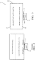
Fig. 2 is a side-view of a known radar assembly in accordance with one embodiment; -
Fig. 3 is a side-view of the radar assembly ofFig. 1 in accordance with one embodiment; -
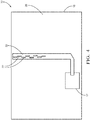
Fig. 4 is a top-view of the radar assembly ofFig. 1 in accordance with one embodiment; -
Fig. 5A is a sectional top-view of an L-shaped transition-feature of the radar assembly ofFig. 1 in accordance with one embodiment; -
Fig. 5B is a sectional top-view of a U-shaped transition-feature of the radar assembly ofFig. 1 in accordance with one embodiment; -
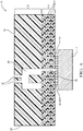
Fig. 6 is a sectional side-view of the radar assembly ofFig. 1 in accordance with one embodiment; -
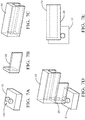
Figs. 7A, 7B, 7C, 7D, and 7E are various views partial assembles of the radar assembly ofFig. 1 in accordance with one embodiment; -
Figs. 8A, 8B, 8C, and 8D are various views an antenna-element of the radar assembly ofFig. 1 in accordance with one embodiment; and -
Figs. 9A and 9B are graphs of performance characteristics of the radar assembly ofFig. 1 in accordance with one embodiment. - Reference will now be made in detail to embodiments, examples of which are illustrated in the accompanying drawings. In the following detailed description, numerous specific details are set forth in order to provide a thorough understanding of the various described embodiments. However, it will be apparent to one of ordinary skill in the art that the various described embodiments may be practiced without these specific details. In other instances, well-known methods, procedures, components, circuits, and networks have not been described in detail so as not to unnecessarily obscure aspects of the embodiments.
- 'One or more' includes a function being performed by one element, a function being performed by more than one element, e.g., in a distributed fashion, several functions being performed by one element, several functions being performed by several elements, or any combination of the above.
- It will also be understood that, although the terms first, second, etc. are, in some instances, used herein to describe various elements, these elements should not be limited by these terms. These terms are only used to distinguish one element from another. For example, a first contact could be termed a second contact, and, similarly, a second contact could be termed a first contact, without departing from the scope of the various described embodiments. The first contact and the second contact are both contacts, but they are not the same contact.
- The terminology used in the description of the various described embodiments herein is for describing embodiments only and is not intended to be limiting. As used in the description of the various described embodiments and the appended claims, the singular forms "a", "an" and "the" are intended to include the plural forms as well, unless the context clearly indicates otherwise. It will also be understood that the term "and/or" as used herein refers to and encompasses all possible combinations of one or more of the associated listed items. It will be further understood that the terms "includes," "including," "comprises," and/or "comprising," when used in this specification, specify the presence of stated features, integers, steps, operations, elements, and/or components, but do not preclude the presence or addition of one or more other features, integers, steps, operations, elements, components, and/or groups thereof.
- As used herein, the term "if' is, optionally, construed to mean "when" or "upon" or "in response to determining" or "in response to detecting," depending on the context. Similarly, the phrase "if it is determined" or "if [a stated condition or event] is detected" is, optionally, construed to mean "upon determining" or "in response to determining" or "upon detecting [the stated condition or event]" or "in response to detecting [the stated condition or event]," depending on the context.
- Automotive radars are often required to have a high gain with a minimum aperture size and a low cost. Typically, radar-systems for automotive applications include multiple printed circuit boards (PCBs) which contain feed networks and radiators. However, the dielectric loss of such systems can be significant, especially when low cost printed-circuit-board materials are used. Described herein is a radar assembly that may be part of a radar-system used to detect objects proximate to a host-vehicle. The host-vehicle may be characterized as an automated vehicle, and may be referred to by some as an automated-mobility-on-demand (AMOD) type of vehicle. The host-vehicle may be operated in an automated-mode, i.e. a fully autonomous mode, where a human-operator of the host-vehicle may do little more than designate a destination to operate the host-vehicle. Accordingly, the host-vehicle may be referred to as an automated vehicle. However, it is contemplated that the teachings presented herein are useful when the host-vehicle is operated in a manual-mode where the degree or level of automation may be little more than providing an audible or visual warning to the human-operator who is generally in control of the steering, accelerator, and brakes of the host-vehicle. For example, the radar-system may merely assist the human-operator as needed to change lanes and/or avoid interference with and/or a collision with, for example, an object such as another-vehicle, a pedestrian, or a road sign.
- Described herein is a radar assembly that uses an innovative way to directly connect a monolithic-microwave-integrated-circuit (MMIC) to an air waveguide which radiates a radar-signal through radiation-slots formed in the waveguide, and does so without any substantive dielectric loss, while also providing for reduced cost. In one embodiment, the radar assembly or radar-system is based on a single FR4 circuit board that includes conductor layers for radar control-signal routing, an MMIC to ridge air waveguide transition or transition-feature, a ridge-air-waveguide, and air waveguide radiator-slots. The MMIC is preferably directly soldered on bottom of the FR4 circuit board using a solder-ball reflow process. Multiple layers of metal conductor in the FR4 circuit board are allocated for radar control-signals, i.e. relatively low-frequency. In one embodiment, air cavities are cut in FR4 then are plated with copper to form the transition-feature, the air waveguide, and radiation-slots for the relatively high-frequency signals emitted and detected by the radar-system.
-
Fig. 1 illustrates a non-limiting example of aradar assembly 10, hereafter often referred to as theassembly 10, which may be part of a radar-system (not shown) that includes, for example, but is not limited to, a housing and mounting hardware for theassembly 10, and/or additional electronics for controlling or selecting radar-signals emitted by theassembly 10 and processing radar-signals detected using theassembly 10 to detect and track targets proximate to the radar-system. - The
assembly 10 includes a monolithic-microwave-integrated-circuit 12 (MMIC 12). TheMMIC 12 includes anarrangement 14, seeFigs. 5A and 5B , of solder-balls 16 configured to couple relatively high-frequency, e.g. greater than 10GHz, radar-signals into or out of theMMIC 12, which may be emitted and/or detected by theMMIC 12, which is not shown inFigs. 5A and 5B . As will be recognized by those in the art, the MMIC 12 may also input and output relatively low-frequency signals, e.g. less than 10MHz, that may be commonly called control-signals. Those control-signals may also be connected or propagated via other-solder-balls that may also be used to directly attach the MMIC 12 to a PCB. - The
assembly 10 includes a single printed-circuit-board 18 (PCB 18). As used herein, the modifier 'single' is used to exclude or avoid or distinguish from radar-assembly designs and prior art with multiple circuit boards and/or multiple types of circuit boards, i.e. designs that used more than one type of dielectric materials for forming the substrates of the multiple circuit boards that may be layered together to form a unified circuit board. By way of further example,Fig. 2 shows an example of multiple types (e.g. FR4 and R03003 from Rogers Corporation) of circuit boards layered together. RO3003 is a known substrate material often used for high-frequency applications, e.g. radar, because of the dielectric properties, e.g. the dielectric-constant or relative-permittivity of substrate material. By contrast, thePCB 18 of theradar assembly 10 described herein is advantageously formed of a single type of laminate-material, for example FR4, as shown inFig. 3 . Also, as used herein, the modifier 'directly' is used to exclude or avoid or distinguish from designs and prior art that suggest using a small printed circuit board formed of high-frequency material (e.g. RO3003) between a relatively low-frequency circuit board and/or antenna-elements of theassembly 10 or the system. - The
assembly 10 includes at least one instance of an antenna-element 20 as shown inFig. 4 , or may include multiple instances of the antenna-element 20 as shown inFig. 1 . The antenna-element 20 may be characterize as integral with or integral to the PCB 18, i.e. is built into the PCB 18 or fabricated at the same time the PCB 18 is fabricated. Alternatively, it is contemplated that the antenna-element 20 could be formed of a separate sheet of formed (e.g. stamped/punched) metal or foil to define antenna-element 20. The antenna-element 20 includes, i.e. is configure to define, one or more radiation-slots 22 configured to couple radar-signals into the antenna-element from the surrounding environment (i.e. receive radar-signals), and/or out of the antenna-element into (i.e. broadcast radar-signals). - The antenna-
element 20 includes an air-waveguide, in particular, a ridge-air-waveguide 24 configured to propagate radar-signals to or from the one or more radiation-slots 22. As used herein, the ridge-air-waveguide 24 has a U-shaped cross-section as shown inFigs. 8B and 8D . The U-shaped cross-section of the ridge-air-waveguide 24 is advantageously used so that the actual-width of the ridge-air-waveguide 24 (the width of the U) is small enough so the input/output ends of multiple instances of the antenna-element 20 can be arranged directly over theMMIC 12. As those in the art will recognized, the effective-width or the electrical-width of ridge-air-waveguide 24 is selected based on the wavelength of the radar-signals, where the effective-width or the electrical-width corresponds to the length of a line that defines the U. That is, the effective-width or the electrical-width of ridge-air-waveguide 24 is greater than the actual-width of the ridge-air-waveguide 24. - By way of example and not limitation, the air-cavities that define the antenna-
elements 20 may be formed by removing areas of thesubstrate 26, and then various surfaces including some or all of those created by the removal of areas of thesubstrate 26 are plated with, for example, copper to form, for example, the ridge-air-waveguide 24 and the radiation-slots 22 of the antenna-element 20.Figs. 8A, 8B, 8C, and 8D illustrate non-limiting examples of various structures, e.g. the ridge-air-waveguide 24 and the radiation-slots 22 formed by the plating with all other parts of thePCB 18 being removed. It is noted that only the metal plating is shown, and the material that forms thesubstrate 26 is not shown inFigs. 8A, 8B, 8C, and 8D . - With the termination ends of the antenna-
elements 20 sized as described above and arranged directly over theMMIC 12, which in this example is about ten-millimeters on a side, it is possible to avoid the added expense and complexity of using a high-frequency substrate to provide for a means to distribute radar signals from the relatively small area of theMMIC 12 to a larger area necessitated by the antenna-elements 20 not having or being based on or distributed by one or more instances of the ridge-air-waveguide 24. To complete the connection between theMMIC 12 and the antenna-element 20, thePCB 18 includes a transition-feature 28 configured to couple radar-signals between thearrangement 14 of solder-balls 16 and the ridge-air-waveguide 24 of the antenna-element 20. The transition-feature 28 is an air-waveguide that is characterized as a slot, and the slot extends between thearrangement 14 of solder-balls 16 and the ridge-air-waveguide 24.Fig. 6 illustrates a non-limiting example of a sectional end-view of an embodiment of theassembly 10 that suggests the relationship between the transition-feature 28, the ridge-air-waveguide 24, and the radiation-slots 22. -
Fig. 5A shows a non-limiting example of part of theassembly 10 where thearrangement 14 of solder-balls 16 is characterized as a solder-ball-pair 14A. That two solder-balls are used is typically determined by the design or configuration of the radar-signal input/output of theMMIC 12. For the solder-ball-pair 14A it may be advantageous for the transition-feature 28 to be configured as or characterized as an L-shaped-slot.Figs. 7A, 7B, 7C, 7D, and 7E show various perspective views of theMMIC 12, the transition-feature 28 and the ridge-air-waveguide 24. Signals to/from theMMIC 12 are electromagnetically coupled to the transition-feature 28, which is an "L" shaped slot, to/from bottom of the transition-feature 28, and the upper side of the transition-feature 28 feeds the end of a ridge-air-waveguide 24. Note that the end of the ridge part of the ridge-air-waveguide 24 is not touching the end wall of the ridge-air-waveguide 24. The topology of this transition makes it possible for the termination ends of the antenna-element 20 to be narrow enough to fit seven ridge air waveguides to the seven RF ports of the relatively small MMIC as shown inFig. 1 . -
Fig. 5B shows a non-limiting example of part of theassembly 10 where thearrangement 14 of solder-balls 16 is characterized as a solder-ball-trio 14B. As above, that three solder-balls are used is generally determined by the design or configuration of the radar-signal input/output of theMMIC 12. For the solder-ball-trio 14B it may be advantageous for the transition-feature 28 to be configured as or characterized as a U-shaped-slot. Note that the end of the ridge part of the ridge-air-waveguide 24 is not touching the end wall of the ridge-air-waveguide 24. - The radiation-
slots 22 depicted inFigs. 8A-8D are opened on the top side or broad side of the ridge-air-waveguide 24, i.e. the top portion of an upside-down U, thereby forming what some refer to as an end-fed waveguide slot array antenna. The width of the ridge-air-waveguide 24 allows a radiator formed of multiple antenna-elements that is narrow enough to form an array without grating lobes. The cross section of the ridge-air-waveguide 24 can be individually optimized for transition and for radiator, a taper in between can bridge the two together.Fig. 1 illustrates a design example for radar-signals of 76.5GHz, where four receive antennas are separated by half wavelengths, and the three transmit antennas are separated by two and half wavelengths. Matching at the ports or radar-signal inputs/outputs of the MMIC is good, radiation pattern has a wide field of view in azimuth, and a 10deg beam width in elevation with side-lobe below -20dB, as shown inFigs 9A and 9B . Advantageously, the design is purposely selected for typical PCB fabrication processes and for minimal manufactural cost. - Referring again to
Fig. 6 , in one embodiment theassembly 10 includes a monolithic-microwave-integrated-circuit 12 (MMIC 12), and a single printed-circuit-board 18 (PCB 18) formed of a single type of laminate-material and directly attached to theMMIC 12. TheMMIC 12 includes anarrangement 14 of solder-balls 16 configured to couple radar-signals into or out of theMMIC 12. ThePCB 18 includes alower portion 30 adjacent to theMMIC 12 and an upper-portion 32 opposite the lower-portion 30 with respect to theMMIC 12. The upper-portion 32 includes an antenna-element 20 that includes one or more radiation-slots 22 configured to couple radar-signals into or out of the antenna-element 20, and a ridge-air-waveguide 24 configured to propagate radar-signals to or from the one or more radiation-slots 22. The lower-portion 30 includes one or more conductor-layers 34 configured to communicate one or more control-signals to theMMIC 12, and a transition-feature 28 configured to couple radar-signals between thearrangement 14 of solder-balls 16 and the ridge-air-waveguide 24. The transition-feature 28 is characterized as a slot that extends through the lower-portion 30 between thearrangement 14 of solder-balls 16 and the ridge-air-waveguide 24. The surfaces that define the ridge-air-waveguide 24 and the transition-feature 28 are plated with metal. - Also described herein, a printed-circuit-board 18 (PCB 18) for a
radar assembly 10 is provided. ThePCB 18 includes asubstrate 26 formed of a single type of laminate-material, and an array 36 of solder-pads 38 on a surface of thesubstrate 26. The array 36 of solder-pads 38 is configured for making a direct connection to anarrangement 14 of solder-balls 16 of a monolithic-microwave-integrated-circuit 12 orMMIC 12. Thearrangement 14 of solder-balls 16 configured to couple radar-signals into or out of theMMIC 12. ThePCB 18 includes or defines alower portion 30 adjacent to the solder-pads and an upper-portion 32 opposite the lower-portion 30 with respect to the solder-pads 38. The upper-portion 32 includes an antenna-element 20 that includes or defines one or more radiation-slots 22 configured to couple radar-signals into or out of the antenna-element 20, and a ridge-air-waveguide 24 configured to propagate radar-signals to or from the one or more radiation-slots 22. Thelower portion 30 includes one or more conductor-layers 34 configured to communicate one or more control-signals to theMMIC 12, and a transition-feature 28 configured to couple radar-signals through the lower-layer between thearrangement 14 of solder-balls 16 and the ridge-air-waveguide 24. The transition-feature 28 is characterized as a slot that extends through the lower-portion 30 between thearrangement 14 of solder-balls 16 and the ridge-air-waveguide 24. - If the
arrangement 14 of solder-balls 16 is characterized as a solder-ball-pair 14A, then the transition-feature 28 is preferably, i.e. is characterized as, an L-shaped-slot. If thearrangement 14 of solder-balls 16 is characterized as a solder-ball-trio 14B, then the transition-feature 28 is preferably, i.e. is characterized, as a U-shaped-slot. If dielectric material such as FR4 is used for thesubstrate 26, the air cavity surfaces that define the ridge-air-waveguide 24 and the transition-feature 28 and radiation-slots 22 may be plated with metal. However, plating is not necessary if the upper-portion 32 is built from formed/stamped metal foil. - Accordingly, a radar assembly 10 (the assembly 10), and a printed-circuit-board 18 (PCB 18) are provided. The narrow air waveguides provided by the ridge-air-
waveguide 24 in combination with a transition air wave guide provided or defined by the transition-feature 28 described herein result in a means to transmit and receive radar-signal with very little or no transmission losses, while being more economical to manufacture that prior radar assemblies. The assembly is designed/configured to be compatible with known printed circuit board fabrication processes. - While this invention has been described in terms of the preferred embodiments thereof, it is not intended to be so limited, but rather only to the extent set forth in the claims that follow.
Claims (15)
- A radar assembly (10), said assembly (10) comprising:a monolithic-microwave-integrated-circuit (12), wherein the monolithic-microwave-integrated-circuit (12) includes an arrangement (14) of solder-balls (16) configured to couple radar-signals into or out of the monolithic-microwave-integrated-circuit (12);an antenna-element (20) that includes one or more radiation-slots (22) configured to couple radar-signals into or out of the antenna-element (20), and a ridge-air-waveguide (24) configured to propagate radar-signals to or from the one or more radiation-slots (22); anda single printed-circuit-board (18) directly attached to the monolithic-microwave-integrated-circuit (12), said single printed-circuit-board (18) includes a transition-feature (28) configured to couple radar-signals between the arrangement (14) of solder-balls (16) and the ridge-air-waveguide (24), wherein the transition-feature (28) is characterized as a slot that extends between the arrangement (14) of solder-balls (16) and the ridge-air-waveguide (24).
- The assembly (10) in accordance with claim 1, wherein the arrangement (14) of solder-balls (16) is characterized as a solder-ball-pair (14A), and the transition-feature (28) characterized as an L-shaped-slot.
- The assembly (10) in accordance with claim 1, wherein the arrangement (14) of solder-balls (16) is characterized as a solder-ball-trio (14B), and the transition-feature (28) characterized as a U-shaped-slot.
- The assembly (10) in accordance with any of the previous claims, wherein the single printed-circuit-board (18) is formed of a single type of laminate-material.
- The assembly (10) in accordance with claim 4, wherein the type of the laminate-material is FR-4.
- The assembly (10) in accordance with claim 4, wherein the antenna-element (20) is characterized as integral with the single printed-circuit-board (18).
- The assembly (10) in accordance with any of the previous claims, wherein surfaces that define the ridge-air-waveguide (24) and the transition-feature (28) are plated with metal.
- The assembly (10) in accordance with any of the previous claims, wherein the assembly (10) includes other-solder-balls (16) that directly attach the monolithic-microwave-integrated-circuit (12) to the single printed-circuit-board (18).
- A radar assembly (10), said assembly (10) comprising:a monolithic-microwave-integrated-circuit (12), wherein the monolithic-microwave-integrated-circuit (12) includes an arrangement (14) of solder-balls (16) configured to couple radar-signals into or out of the monolithic-microwave-integrated-circuit (12); anda single printed-circuit-board (18) formed of a single type of laminate-material and directly attached to the monolithic-microwave-integrated-circuit (12), said single printed-circuit-board (18) includes a lower portion (30) adjacent to the monolithic-microwave-integrated-circuit (12) and an upper-portion (32) opposite the lower-portion (30) with respect to the monolithic-microwave-integrated-circuit (12),said upper-portion (32) includes an antenna-element (20) that includes one or more radiation-slots (22) configured to couple radar-signals into or out of the antenna-element (20), and a ridge-air-waveguide (24) configured to propagate radar-signals to or from the one or more radiation-slots (22),said lower-portion (30) includes one or more conductor-layers (34) configured to communicate one or more control-signals to the monolithic-microwave-integrated-circuit (12), anda transition-feature (28) configured to couple radar-signals between the arrangement (14) of solder-balls (16) and the ridge-air-waveguide (24), wherein the transition-feature (28) is characterized as a slot that extends through the lower-portion (30) between the arrangement (14) of solder-balls (16) and the ridge-air-waveguide (24), and surfaces that define the ridge-air-waveguide (24) and the transition-feature (28) are plated with metal.
- The assembly (10) in accordance with claim 9, wherein the arrangement (14) of solder-balls (16) is characterized as a solder-ball-pair (14A), and the transition-feature (28) characterized as an L-shaped-slot.
- The assembly (10) in accordance with claim 9, wherein the arrangement (14) of solder-balls (16) is characterized as a solder-ball-trio (14B), and the transition-feature (28) characterized as a U-shaped-slot.
- A printed-circuit-board (18) for a radar assembly (10), said printed-circuit-board (18) comprising:a substrate (26) formed of a single type of laminate-material;an arrangement (14) of solder-pads (38) on a surface of the substrate (26), said arrangement (14) of solder-pads (38) configured for making a direct connection to an arrangement (14) of solder-balls (16) of a monolithic-microwave-integrated-circuit (12), said arrangement (14) of solder-balls (16) configured to couple radar-signals into or out of the monolithic-microwave-integrated-circuit (12);said printed-circuit-board (18) includes a lower portion (30) adjacent to the solder-pads (38) and an upper-portion (32) opposite the lower-portion (30) with respect to the solder-pads (38),said upper-portion (32) includes an antenna-element (20) that includes one or more radiation-slots (22) configured to couple radar-signals into or out of the antenna-element (20), and a ridge-air-waveguide (24) configured to propagate radar-signals to or from the one or more radiation-slots (22),said lower portion (30) includes one or more conductor-layers (34) configured to communicate one or more control-signals to the monolithic-microwave-integrated-circuit (12), and a transition-feature (28) configured to couple radar-signals through the lower-layer between the arrangement (14) of solder-balls (16) and the ridge-air-waveguide (24), said transition-feature (28) characterized as a slot that extends through the lower-portion (30) between the arrangement (14) of solder-balls (16) and the ridge-air-waveguide (24).
- The printed-circuit-board (18) in accordance with claim 12, wherein the arrangement (14) of solder-balls (16) is characterized as a solder-ball-pair (14A), and the transition-feature (28) characterized as an L-shaped-slot.
- The printed-circuit-board (18) in accordance with claim 12, wherein the arrangement (14) of solder-balls (16) is characterized as a solder-ball-trio (14B), and the transition-feature (28) characterized as a U-shaped-slot.
- The printed-circuit-board (18) in accordance with any of the previous claims, wherein surfaces that define the ridge-air-waveguide (24) and the transition-feature (28) are plated with metal.
Applications Claiming Priority (2)
| Application Number | Priority Date | Filing Date | Title |
|---|---|---|---|
| US201862752130P | 2018-10-29 | 2018-10-29 | |
| US16/175,501 US11011816B2 (en) | 2018-10-29 | 2018-10-30 | Radar assembly with a slot transition through a printed circuit board |
Publications (2)
| Publication Number | Publication Date |
|---|---|
| EP3647807A1 true EP3647807A1 (en) | 2020-05-06 |
| EP3647807B1 EP3647807B1 (en) | 2023-12-13 |
Family
ID=68084605
Family Applications (1)
| Application Number | Title | Priority Date | Filing Date |
|---|---|---|---|
| EP19199951.5A Active EP3647807B1 (en) | 2018-10-29 | 2019-09-26 | Radar assembly with a slot transition through a printed circuit board |
Country Status (3)
| Country | Link |
|---|---|
| US (1) | US11011816B2 (en) |
| EP (1) | EP3647807B1 (en) |
| CN (1) | CN111123210B (en) |
Cited By (3)
| Publication number | Priority date | Publication date | Assignee | Title |
|---|---|---|---|---|
| DE102023203759A1 (en) | 2023-04-24 | 2024-10-24 | Robert Bosch Gesellschaft mit beschränkter Haftung | radar sensor with multiple radar chip units |
| US12230857B2 (en) | 2021-11-30 | 2025-02-18 | Navico, Inc. | Radar waveguide and choke assembly |
| US12451578B2 (en) | 2022-12-30 | 2025-10-21 | Nxp B.V. | Interposers with millimeter-wave coaxial-to-waveguide transistions |
Families Citing this family (20)
| Publication number | Priority date | Publication date | Assignee | Title |
|---|---|---|---|---|
| DE102018203106A1 (en) * | 2018-03-01 | 2019-09-05 | Conti Temic Microelectronic Gmbh | Radar system for detecting the surroundings of a motor vehicle with a plastic antenna |
| US11454720B2 (en) * | 2018-11-28 | 2022-09-27 | Magna Electronics Inc. | Vehicle radar system with enhanced wave guide antenna system |
| DE102020209307A1 (en) * | 2020-07-23 | 2022-01-27 | Robert Bosch Gesellschaft mit beschränkter Haftung | Radar sensor with waveguide structure |
| US20230268666A1 (en) * | 2020-07-28 | 2023-08-24 | Sensata Technologies, Inc. | Modular waveguide to printed circuit board interconnected radar design |
| US11901601B2 (en) | 2020-12-18 | 2024-02-13 | Aptiv Technologies Limited | Waveguide with a zigzag for suppressing grating lobes |
| US11749883B2 (en) | 2020-12-18 | 2023-09-05 | Aptiv Technologies Limited | Waveguide with radiation slots and parasitic elements for asymmetrical coverage |
| US12058804B2 (en) | 2021-02-09 | 2024-08-06 | Aptiv Technologies AG | Formed waveguide antennas of a radar assembly |
| US11962085B2 (en) | 2021-05-13 | 2024-04-16 | Aptiv Technologies AG | Two-part folded waveguide having a sinusoidal shape channel including horn shape radiating slots formed therein which are spaced apart by one-half wavelength |
| US11749884B2 (en) * | 2021-05-17 | 2023-09-05 | HJWAVE Co., Ltd. | Multi-layer antenna structure supporting wide band and wide angle |
| US12355151B2 (en) | 2021-05-17 | 2025-07-08 | HJWAVE Co., Ltd. | Antenna structure with reduced angle error |
| US11616282B2 (en) | 2021-08-03 | 2023-03-28 | Aptiv Technologies Limited | Transition between a single-ended port and differential ports having stubs that match with input impedances of the single-ended and differential ports |
| US12055654B2 (en) * | 2021-08-20 | 2024-08-06 | Gm Cruise Holdings Llc | Scanning radar system with substrate integrated waveguides and heat dissipating structures |
| US12456816B2 (en) * | 2022-05-02 | 2025-10-28 | Aptiv Technologies AG | Waveguide with slot antennas and reflectors |
| US12613334B2 (en) * | 2022-06-28 | 2026-04-28 | Magna Electronics, Llc | Integrated circuit to waveguide transitional structures and related sensor assemblies |
| US12451579B2 (en) | 2022-12-30 | 2025-10-21 | Nxp B.V. | Interposers with millimeter-wave transitions |
| US12537308B2 (en) | 2023-01-24 | 2026-01-27 | Aptiv Technologies AG | Symmetrical two-piece waveguide |
| US12148992B2 (en) | 2023-01-25 | 2024-11-19 | Aptiv Technologies AG | Hybrid horn waveguide antenna |
| US12627020B2 (en) | 2023-05-18 | 2026-05-12 | Aptiv Technologies AG | Waveguide with a curved-wall low-pass filter |
| DE102023211697A1 (en) * | 2023-11-23 | 2025-05-28 | Continental Autonomous Mobility Germany GmbH | Waveguide arrangement, radar sensor and vehicle |
| US20260036670A1 (en) * | 2024-04-19 | 2026-02-05 | Aptiv Technologies AG | Innovative Open Waveguide Bend for Leakage Mitigation |
Citations (3)
| Publication number | Priority date | Publication date | Assignee | Title |
|---|---|---|---|---|
| WO2004063767A1 (en) * | 2003-01-13 | 2004-07-29 | Epcos Ag | Radar-transceiver for microwave and millimetre applications |
| US20060202312A1 (en) * | 2005-03-09 | 2006-09-14 | Fujitsu Limited | Radio-frequency module for communication and method of manufacturing the same |
| DE102014200660A1 (en) * | 2014-01-16 | 2015-07-16 | Conti Temic Microelectronic Gmbh | Transmitting and receiving unit for radar signals and method for producing the same |
Family Cites Families (10)
| Publication number | Priority date | Publication date | Assignee | Title |
|---|---|---|---|---|
| JP4394147B2 (en) * | 2006-02-06 | 2010-01-06 | 三菱電機株式会社 | High frequency module |
| US9196958B2 (en) * | 2012-07-26 | 2015-11-24 | Apple Inc. | Antenna structures and shield layers on packaged wireless circuits |
| WO2014108744A1 (en) * | 2013-01-09 | 2014-07-17 | Freescale Semiconductor, Inc. | Electronic high frequency device and manufacturing method |
| EP2973863B1 (en) * | 2013-03-15 | 2017-12-06 | Flextronics AP LLC | Powder coating method and apparatus for absorbing electromagnetic interference (emi) |
| DE102016125419B4 (en) * | 2015-12-24 | 2022-10-20 | Nidec Elesys Corporation | Waveguide device, slot antenna and radar, radar system, and wireless communication system with the slot antenna |
| JP2019047141A (en) * | 2016-03-29 | 2019-03-22 | 日本電産エレシス株式会社 | Microwave IC waveguide device module, radar device and radar system |
| DE112016006695B4 (en) * | 2016-04-01 | 2026-01-29 | Intel Corporation | Housing on antenna housing and method for its manufacture |
| DE102016212129B4 (en) * | 2016-07-04 | 2022-05-19 | Schweizer Electronic Ag | Radio frequency transmission/reception element and method of manufacturing a radio frequency transmission/reception element |
| EP3364457A1 (en) * | 2017-02-15 | 2018-08-22 | Nxp B.V. | Integrated circuit package including an antenna |
| JP2018164252A (en) * | 2017-03-24 | 2018-10-18 | 日本電産株式会社 | Slot array antenna, and radar having the same |
-
2018
- 2018-10-30 US US16/175,501 patent/US11011816B2/en active Active
-
2019
- 2019-09-26 EP EP19199951.5A patent/EP3647807B1/en active Active
- 2019-10-28 CN CN201911030880.6A patent/CN111123210B/en active Active
Patent Citations (3)
| Publication number | Priority date | Publication date | Assignee | Title |
|---|---|---|---|---|
| WO2004063767A1 (en) * | 2003-01-13 | 2004-07-29 | Epcos Ag | Radar-transceiver for microwave and millimetre applications |
| US20060202312A1 (en) * | 2005-03-09 | 2006-09-14 | Fujitsu Limited | Radio-frequency module for communication and method of manufacturing the same |
| DE102014200660A1 (en) * | 2014-01-16 | 2015-07-16 | Conti Temic Microelectronic Gmbh | Transmitting and receiving unit for radar signals and method for producing the same |
Cited By (3)
| Publication number | Priority date | Publication date | Assignee | Title |
|---|---|---|---|---|
| US12230857B2 (en) | 2021-11-30 | 2025-02-18 | Navico, Inc. | Radar waveguide and choke assembly |
| US12451578B2 (en) | 2022-12-30 | 2025-10-21 | Nxp B.V. | Interposers with millimeter-wave coaxial-to-waveguide transistions |
| DE102023203759A1 (en) | 2023-04-24 | 2024-10-24 | Robert Bosch Gesellschaft mit beschränkter Haftung | radar sensor with multiple radar chip units |
Also Published As
| Publication number | Publication date |
|---|---|
| CN111123210A (en) | 2020-05-08 |
| CN111123210B (en) | 2023-09-05 |
| US20200136225A1 (en) | 2020-04-30 |
| EP3647807B1 (en) | 2023-12-13 |
| US11011816B2 (en) | 2021-05-18 |
Similar Documents
| Publication | Publication Date | Title |
|---|---|---|
| EP3647807B1 (en) | Radar assembly with a slot transition through a printed circuit board | |
| US11604273B2 (en) | Radar system for detecting the environment of a motor vehicle having a plastic antenna | |
| US20210036393A1 (en) | Radar Assembly with Rectangular Waveguide to Substrate Integrated Waveguide Transition | |
| US11183751B2 (en) | Antenna device with direct differential input useable on an automated vehicle | |
| KR101621480B1 (en) | Transit structure of waveguide and dielectric waveguide | |
| US10295652B2 (en) | Vehicle radar system for detecting the surroundings | |
| EP1418643A2 (en) | Microstrip antenna array with periodic filters | |
| US12313767B2 (en) | Method for manufacturing a radar sensor | |
| US20180231657A1 (en) | Vehicle radar system with radar embedded into radome | |
| US10014583B2 (en) | Meander-type, frequency-scanned antenna with reduced beam squint for an automated vehicle radar system | |
| US10141636B2 (en) | Volumetric scan automotive radar with end-fire antenna on partially laminated multi-layer PCB | |
| US11552379B2 (en) | Transition from a stripline to a waveguide | |
| CA2397748A1 (en) | Antenna horn and associated methods | |
| WO1999027606A2 (en) | Microstrip arrangement | |
| US10714817B2 (en) | Antenna device for a radar detector having at least two radiation directions, and motor vehicle having at least one radar detector | |
| KR20150125262A (en) | Multi layer board and manufacturing method of it | |
| CN103098301B (en) | Planar combination antenna with antenna elements arranged in multiple planes | |
| US6509874B1 (en) | Reactive matching for waveguide-slot-microstrip transitions | |
| US11011814B2 (en) | Coupling comprising a conductive wire embedded in a post-wall waveguide and extending into a hollow tube waveguide | |
| EP4130783A1 (en) | Radar system for a vehicle | |
| CN217306728U (en) | Power divider, antenna device, radio device, and apparatus | |
| CN118285019A (en) | Radar sensor and manufacturing method | |
| US11621464B2 (en) | Waveguide assembly | |
| KR20240058150A (en) | Radar sensor with waveguide structure | |
| KR102890235B1 (en) | Microstrip antenna and radar device for vehicle including the same |
Legal Events
| Date | Code | Title | Description |
|---|---|---|---|
| PUAI | Public reference made under article 153(3) epc to a published international application that has entered the european phase |
Free format text: ORIGINAL CODE: 0009012 |
|
| STAA | Information on the status of an ep patent application or granted ep patent |
Free format text: STATUS: THE APPLICATION HAS BEEN PUBLISHED |
|
| AK | Designated contracting states |
Kind code of ref document: A1 Designated state(s): AL AT BE BG CH CY CZ DE DK EE ES FI FR GB GR HR HU IE IS IT LI LT LU LV MC MK MT NL NO PL PT RO RS SE SI SK SM TR |
|
| AX | Request for extension of the european patent |
Extension state: BA ME |
|
| STAA | Information on the status of an ep patent application or granted ep patent |
Free format text: STATUS: REQUEST FOR EXAMINATION WAS MADE |
|
| 17P | Request for examination filed |
Effective date: 20201105 |
|
| RBV | Designated contracting states (corrected) |
Designated state(s): AL AT BE BG CH CY CZ DE DK EE ES FI FR GB GR HR HU IE IS IT LI LT LU LV MC MK MT NL NO PL PT RO RS SE SI SK SM TR |
|
| STAA | Information on the status of an ep patent application or granted ep patent |
Free format text: STATUS: EXAMINATION IS IN PROGRESS |
|
| 17Q | First examination report despatched |
Effective date: 20220331 |
|
| RAP3 | Party data changed (applicant data changed or rights of an application transferred) |
Owner name: APTIV TECHNOLOGIES LIMITED |
|
| GRAP | Despatch of communication of intention to grant a patent |
Free format text: ORIGINAL CODE: EPIDOSNIGR1 |
|
| STAA | Information on the status of an ep patent application or granted ep patent |
Free format text: STATUS: GRANT OF PATENT IS INTENDED |
|
| INTG | Intention to grant announced |
Effective date: 20230905 |
|
| GRAS | Grant fee paid |
Free format text: ORIGINAL CODE: EPIDOSNIGR3 |
|
| GRAA | (expected) grant |
Free format text: ORIGINAL CODE: 0009210 |
|
| STAA | Information on the status of an ep patent application or granted ep patent |
Free format text: STATUS: THE PATENT HAS BEEN GRANTED |
|
| AK | Designated contracting states |
Kind code of ref document: B1 Designated state(s): AL AT BE BG CH CY CZ DE DK EE ES FI FR GB GR HR HU IE IS IT LI LT LU LV MC MK MT NL NO PL PT RO RS SE SI SK SM TR |
|
| REG | Reference to a national code |
Ref country code: GB Ref legal event code: FG4D |
|
| REG | Reference to a national code |
Ref country code: CH Ref legal event code: EP |
|
| P01 | Opt-out of the competence of the unified patent court (upc) registered |
Effective date: 20231113 |
|
| REG | Reference to a national code |
Ref country code: DE Ref legal event code: R096 Ref document number: 602019043141 Country of ref document: DE |
|
| REG | Reference to a national code |
Ref country code: IE Ref legal event code: FG4D |
|
| PG25 | Lapsed in a contracting state [announced via postgrant information from national office to epo] |
Ref country code: GR Free format text: LAPSE BECAUSE OF FAILURE TO SUBMIT A TRANSLATION OF THE DESCRIPTION OR TO PAY THE FEE WITHIN THE PRESCRIBED TIME-LIMIT Effective date: 20240314 |
|
| REG | Reference to a national code |
Ref country code: LT Ref legal event code: MG9D |
|
| PG25 | Lapsed in a contracting state [announced via postgrant information from national office to epo] |
Ref country code: LT Free format text: LAPSE BECAUSE OF FAILURE TO SUBMIT A TRANSLATION OF THE DESCRIPTION OR TO PAY THE FEE WITHIN THE PRESCRIBED TIME-LIMIT Effective date: 20231213 |
|
| REG | Reference to a national code |
Ref country code: NL Ref legal event code: MP Effective date: 20231213 |
|
| PG25 | Lapsed in a contracting state [announced via postgrant information from national office to epo] |
Ref country code: ES Free format text: LAPSE BECAUSE OF FAILURE TO SUBMIT A TRANSLATION OF THE DESCRIPTION OR TO PAY THE FEE WITHIN THE PRESCRIBED TIME-LIMIT Effective date: 20231213 |
|
| PG25 | Lapsed in a contracting state [announced via postgrant information from national office to epo] |
Ref country code: LT Free format text: LAPSE BECAUSE OF FAILURE TO SUBMIT A TRANSLATION OF THE DESCRIPTION OR TO PAY THE FEE WITHIN THE PRESCRIBED TIME-LIMIT Effective date: 20231213 Ref country code: GR Free format text: LAPSE BECAUSE OF FAILURE TO SUBMIT A TRANSLATION OF THE DESCRIPTION OR TO PAY THE FEE WITHIN THE PRESCRIBED TIME-LIMIT Effective date: 20240314 Ref country code: ES Free format text: LAPSE BECAUSE OF FAILURE TO SUBMIT A TRANSLATION OF THE DESCRIPTION OR TO PAY THE FEE WITHIN THE PRESCRIBED TIME-LIMIT Effective date: 20231213 Ref country code: BG Free format text: LAPSE BECAUSE OF FAILURE TO SUBMIT A TRANSLATION OF THE DESCRIPTION OR TO PAY THE FEE WITHIN THE PRESCRIBED TIME-LIMIT Effective date: 20240313 |
|
| REG | Reference to a national code |
Ref country code: AT Ref legal event code: MK05 Ref document number: 1640891 Country of ref document: AT Kind code of ref document: T Effective date: 20231213 |
|
| PG25 | Lapsed in a contracting state [announced via postgrant information from national office to epo] |
Ref country code: NL Free format text: LAPSE BECAUSE OF FAILURE TO SUBMIT A TRANSLATION OF THE DESCRIPTION OR TO PAY THE FEE WITHIN THE PRESCRIBED TIME-LIMIT Effective date: 20231213 |
|
| PG25 | Lapsed in a contracting state [announced via postgrant information from national office to epo] |
Ref country code: SE Free format text: LAPSE BECAUSE OF FAILURE TO SUBMIT A TRANSLATION OF THE DESCRIPTION OR TO PAY THE FEE WITHIN THE PRESCRIBED TIME-LIMIT Effective date: 20231213 Ref country code: RS Free format text: LAPSE BECAUSE OF FAILURE TO SUBMIT A TRANSLATION OF THE DESCRIPTION OR TO PAY THE FEE WITHIN THE PRESCRIBED TIME-LIMIT Effective date: 20231213 Ref country code: NO Free format text: LAPSE BECAUSE OF FAILURE TO SUBMIT A TRANSLATION OF THE DESCRIPTION OR TO PAY THE FEE WITHIN THE PRESCRIBED TIME-LIMIT Effective date: 20240313 Ref country code: NL Free format text: LAPSE BECAUSE OF FAILURE TO SUBMIT A TRANSLATION OF THE DESCRIPTION OR TO PAY THE FEE WITHIN THE PRESCRIBED TIME-LIMIT Effective date: 20231213 Ref country code: LV Free format text: LAPSE BECAUSE OF FAILURE TO SUBMIT A TRANSLATION OF THE DESCRIPTION OR TO PAY THE FEE WITHIN THE PRESCRIBED TIME-LIMIT Effective date: 20231213 Ref country code: HR Free format text: LAPSE BECAUSE OF FAILURE TO SUBMIT A TRANSLATION OF THE DESCRIPTION OR TO PAY THE FEE WITHIN THE PRESCRIBED TIME-LIMIT Effective date: 20231213 |
|
| PG25 | Lapsed in a contracting state [announced via postgrant information from national office to epo] |
Ref country code: IS Free format text: LAPSE BECAUSE OF FAILURE TO SUBMIT A TRANSLATION OF THE DESCRIPTION OR TO PAY THE FEE WITHIN THE PRESCRIBED TIME-LIMIT Effective date: 20240413 |
|
| PG25 | Lapsed in a contracting state [announced via postgrant information from national office to epo] |
Ref country code: AT Free format text: LAPSE BECAUSE OF FAILURE TO SUBMIT A TRANSLATION OF THE DESCRIPTION OR TO PAY THE FEE WITHIN THE PRESCRIBED TIME-LIMIT Effective date: 20231213 Ref country code: CZ Free format text: LAPSE BECAUSE OF FAILURE TO SUBMIT A TRANSLATION OF THE DESCRIPTION OR TO PAY THE FEE WITHIN THE PRESCRIBED TIME-LIMIT Effective date: 20231213 |
|
| PG25 | Lapsed in a contracting state [announced via postgrant information from national office to epo] |
Ref country code: SK Free format text: LAPSE BECAUSE OF FAILURE TO SUBMIT A TRANSLATION OF THE DESCRIPTION OR TO PAY THE FEE WITHIN THE PRESCRIBED TIME-LIMIT Effective date: 20231213 |
|
| PG25 | Lapsed in a contracting state [announced via postgrant information from national office to epo] |
Ref country code: SM Free format text: LAPSE BECAUSE OF FAILURE TO SUBMIT A TRANSLATION OF THE DESCRIPTION OR TO PAY THE FEE WITHIN THE PRESCRIBED TIME-LIMIT Effective date: 20231213 Ref country code: SK Free format text: LAPSE BECAUSE OF FAILURE TO SUBMIT A TRANSLATION OF THE DESCRIPTION OR TO PAY THE FEE WITHIN THE PRESCRIBED TIME-LIMIT Effective date: 20231213 Ref country code: RO Free format text: LAPSE BECAUSE OF FAILURE TO SUBMIT A TRANSLATION OF THE DESCRIPTION OR TO PAY THE FEE WITHIN THE PRESCRIBED TIME-LIMIT Effective date: 20231213 Ref country code: IT Free format text: LAPSE BECAUSE OF FAILURE TO SUBMIT A TRANSLATION OF THE DESCRIPTION OR TO PAY THE FEE WITHIN THE PRESCRIBED TIME-LIMIT Effective date: 20231213 Ref country code: IS Free format text: LAPSE BECAUSE OF FAILURE TO SUBMIT A TRANSLATION OF THE DESCRIPTION OR TO PAY THE FEE WITHIN THE PRESCRIBED TIME-LIMIT Effective date: 20240413 Ref country code: EE Free format text: LAPSE BECAUSE OF FAILURE TO SUBMIT A TRANSLATION OF THE DESCRIPTION OR TO PAY THE FEE WITHIN THE PRESCRIBED TIME-LIMIT Effective date: 20231213 Ref country code: CZ Free format text: LAPSE BECAUSE OF FAILURE TO SUBMIT A TRANSLATION OF THE DESCRIPTION OR TO PAY THE FEE WITHIN THE PRESCRIBED TIME-LIMIT Effective date: 20231213 Ref country code: AT Free format text: LAPSE BECAUSE OF FAILURE TO SUBMIT A TRANSLATION OF THE DESCRIPTION OR TO PAY THE FEE WITHIN THE PRESCRIBED TIME-LIMIT Effective date: 20231213 |
|
| PG25 | Lapsed in a contracting state [announced via postgrant information from national office to epo] |
Ref country code: PL Free format text: LAPSE BECAUSE OF FAILURE TO SUBMIT A TRANSLATION OF THE DESCRIPTION OR TO PAY THE FEE WITHIN THE PRESCRIBED TIME-LIMIT Effective date: 20231213 Ref country code: PT Free format text: LAPSE BECAUSE OF FAILURE TO SUBMIT A TRANSLATION OF THE DESCRIPTION OR TO PAY THE FEE WITHIN THE PRESCRIBED TIME-LIMIT Effective date: 20240415 |
|
| PG25 | Lapsed in a contracting state [announced via postgrant information from national office to epo] |
Ref country code: PT Free format text: LAPSE BECAUSE OF FAILURE TO SUBMIT A TRANSLATION OF THE DESCRIPTION OR TO PAY THE FEE WITHIN THE PRESCRIBED TIME-LIMIT Effective date: 20240415 Ref country code: PL Free format text: LAPSE BECAUSE OF FAILURE TO SUBMIT A TRANSLATION OF THE DESCRIPTION OR TO PAY THE FEE WITHIN THE PRESCRIBED TIME-LIMIT Effective date: 20231213 |
|
| REG | Reference to a national code |
Ref country code: DE Ref legal event code: R097 Ref document number: 602019043141 Country of ref document: DE |
|
| PG25 | Lapsed in a contracting state [announced via postgrant information from national office to epo] |
Ref country code: DK Free format text: LAPSE BECAUSE OF FAILURE TO SUBMIT A TRANSLATION OF THE DESCRIPTION OR TO PAY THE FEE WITHIN THE PRESCRIBED TIME-LIMIT Effective date: 20231213 |
|
| PLBE | No opposition filed within time limit |
Free format text: ORIGINAL CODE: 0009261 |
|
| STAA | Information on the status of an ep patent application or granted ep patent |
Free format text: STATUS: NO OPPOSITION FILED WITHIN TIME LIMIT |
|
| PG25 | Lapsed in a contracting state [announced via postgrant information from national office to epo] |
Ref country code: SI Free format text: LAPSE BECAUSE OF FAILURE TO SUBMIT A TRANSLATION OF THE DESCRIPTION OR TO PAY THE FEE WITHIN THE PRESCRIBED TIME-LIMIT Effective date: 20231213 |
|
| PG25 | Lapsed in a contracting state [announced via postgrant information from national office to epo] |
Ref country code: SI Free format text: LAPSE BECAUSE OF FAILURE TO SUBMIT A TRANSLATION OF THE DESCRIPTION OR TO PAY THE FEE WITHIN THE PRESCRIBED TIME-LIMIT Effective date: 20231213 Ref country code: DK Free format text: LAPSE BECAUSE OF FAILURE TO SUBMIT A TRANSLATION OF THE DESCRIPTION OR TO PAY THE FEE WITHIN THE PRESCRIBED TIME-LIMIT Effective date: 20231213 |
|
| 26N | No opposition filed |
Effective date: 20240916 |
|
| PG25 | Lapsed in a contracting state [announced via postgrant information from national office to epo] |
Ref country code: MC Free format text: LAPSE BECAUSE OF FAILURE TO SUBMIT A TRANSLATION OF THE DESCRIPTION OR TO PAY THE FEE WITHIN THE PRESCRIBED TIME-LIMIT Effective date: 20231213 |
|
| REG | Reference to a national code |
Ref country code: DE Ref legal event code: R081 Ref document number: 602019043141 Country of ref document: DE Owner name: APTIV TECHNOLOGIES AG, CH Free format text: FORMER OWNER: APTIV TECHNOLOGIES LIMITED, ST. MICHAEL, BB Ref country code: CH Ref legal event code: PL |
|
| PG25 | Lapsed in a contracting state [announced via postgrant information from national office to epo] |
Ref country code: LU Free format text: LAPSE BECAUSE OF NON-PAYMENT OF DUE FEES Effective date: 20240926 |
|
| REG | Reference to a national code |
Ref country code: BE Ref legal event code: MM Effective date: 20240930 |
|
| PG25 | Lapsed in a contracting state [announced via postgrant information from national office to epo] |
Ref country code: BE Free format text: LAPSE BECAUSE OF NON-PAYMENT OF DUE FEES Effective date: 20240930 |
|
| PG25 | Lapsed in a contracting state [announced via postgrant information from national office to epo] |
Ref country code: CH Free format text: LAPSE BECAUSE OF NON-PAYMENT OF DUE FEES Effective date: 20240930 |
|
| PG25 | Lapsed in a contracting state [announced via postgrant information from national office to epo] |
Ref country code: IE Free format text: LAPSE BECAUSE OF NON-PAYMENT OF DUE FEES Effective date: 20240926 |
|
| PG25 | Lapsed in a contracting state [announced via postgrant information from national office to epo] |
Ref country code: FI Free format text: LAPSE BECAUSE OF FAILURE TO SUBMIT A TRANSLATION OF THE DESCRIPTION OR TO PAY THE FEE WITHIN THE PRESCRIBED TIME-LIMIT Effective date: 20231213 |
|
| PGFP | Annual fee paid to national office [announced via postgrant information from national office to epo] |
Ref country code: DE Payment date: 20250814 Year of fee payment: 7 |
|
| PGFP | Annual fee paid to national office [announced via postgrant information from national office to epo] |
Ref country code: GB Payment date: 20250924 Year of fee payment: 7 |
|
| PGFP | Annual fee paid to national office [announced via postgrant information from national office to epo] |
Ref country code: FR Payment date: 20250908 Year of fee payment: 7 |
|
| PG25 | Lapsed in a contracting state [announced via postgrant information from national office to epo] |
Ref country code: CY Free format text: LAPSE BECAUSE OF FAILURE TO SUBMIT A TRANSLATION OF THE DESCRIPTION OR TO PAY THE FEE WITHIN THE PRESCRIBED TIME-LIMIT; INVALID AB INITIO Effective date: 20190926 |
|
| PG25 | Lapsed in a contracting state [announced via postgrant information from national office to epo] |
Ref country code: HU Free format text: LAPSE BECAUSE OF FAILURE TO SUBMIT A TRANSLATION OF THE DESCRIPTION OR TO PAY THE FEE WITHIN THE PRESCRIBED TIME-LIMIT; INVALID AB INITIO Effective date: 20190926 |