EP3647755A1 - Sensor device with flip-chip die and interposer - Google Patents
Sensor device with flip-chip die and interposer Download PDFInfo
- Publication number
- EP3647755A1 EP3647755A1 EP19203327.2A EP19203327A EP3647755A1 EP 3647755 A1 EP3647755 A1 EP 3647755A1 EP 19203327 A EP19203327 A EP 19203327A EP 3647755 A1 EP3647755 A1 EP 3647755A1
- Authority
- EP
- European Patent Office
- Prior art keywords
- die
- interposer
- vent hole
- lead frame
- active region
- Prior art date
- Legal status (The legal status is an assumption and is not a legal conclusion. Google has not performed a legal analysis and makes no representation as to the accuracy of the status listed.)
- Withdrawn
Links
Images



Classifications
-
- G—PHYSICS
- G01—MEASURING; TESTING
- G01L—MEASURING FORCE, STRESS, TORQUE, WORK, MECHANICAL POWER, MECHANICAL EFFICIENCY, OR FLUID PRESSURE
- G01L19/00—Details of, or accessories for, apparatus for measuring steady or quasi-steady pressure of a fluent medium insofar as such details or accessories are not special to particular types of pressure gauges
- G01L19/06—Means for preventing overload or deleterious influence of the measured medium on the measuring device or vice versa
- G01L19/0627—Protection against aggressive medium in general
- G01L19/0654—Protection against aggressive medium in general against moisture or humidity
-
- B—PERFORMING OPERATIONS; TRANSPORTING
- B81—MICROSTRUCTURAL TECHNOLOGY
- B81B—MICROSTRUCTURAL DEVICES OR SYSTEMS, e.g. MICROMECHANICAL DEVICES
- B81B7/00—Microstructural systems ; Auxiliary parts of microstructural devices or systems
- B81B7/0032—Packages or encapsulation
- B81B7/007—Interconnections between the MEMS and external electrical signals
-
- B—PERFORMING OPERATIONS; TRANSPORTING
- B81—MICROSTRUCTURAL TECHNOLOGY
- B81B—MICROSTRUCTURAL DEVICES OR SYSTEMS, e.g. MICROMECHANICAL DEVICES
- B81B7/00—Microstructural systems ; Auxiliary parts of microstructural devices or systems
- B81B7/0032—Packages or encapsulation
- B81B7/0061—Packages or encapsulation suitable for fluid transfer from the MEMS out of the package or vice versa, e.g. transfer of liquid, gas, sound
-
- B—PERFORMING OPERATIONS; TRANSPORTING
- B81—MICROSTRUCTURAL TECHNOLOGY
- B81C—PROCESSES OR APPARATUS SPECIALLY ADAPTED FOR THE MANUFACTURE OR TREATMENT OF MICROSTRUCTURAL DEVICES OR SYSTEMS
- B81C1/00—Manufacture or treatment of devices or systems in or on a substrate
- B81C1/00015—Manufacture or treatment of devices or systems in or on a substrate for manufacturing microsystems
- B81C1/00261—Processes for packaging MEMS devices
- B81C1/00301—Connecting electric signal lines from the MEMS device with external electrical signal lines, e.g. through vias
-
- B—PERFORMING OPERATIONS; TRANSPORTING
- B81—MICROSTRUCTURAL TECHNOLOGY
- B81C—PROCESSES OR APPARATUS SPECIALLY ADAPTED FOR THE MANUFACTURE OR TREATMENT OF MICROSTRUCTURAL DEVICES OR SYSTEMS
- B81C1/00—Manufacture or treatment of devices or systems in or on a substrate
- B81C1/00015—Manufacture or treatment of devices or systems in or on a substrate for manufacturing microsystems
- B81C1/00261—Processes for packaging MEMS devices
- B81C1/00309—Processes for packaging MEMS devices suitable for fluid transfer from the MEMS out of the package or vice versa, e.g. transfer of liquid, gas, sound
-
- G—PHYSICS
- G01—MEASURING; TESTING
- G01L—MEASURING FORCE, STRESS, TORQUE, WORK, MECHANICAL POWER, MECHANICAL EFFICIENCY, OR FLUID PRESSURE
- G01L19/00—Details of, or accessories for, apparatus for measuring steady or quasi-steady pressure of a fluent medium insofar as such details or accessories are not special to particular types of pressure gauges
- G01L19/0061—Electrical connection means
- G01L19/0069—Electrical connection means from the sensor to its support
-
- G—PHYSICS
- G01—MEASURING; TESTING
- G01L—MEASURING FORCE, STRESS, TORQUE, WORK, MECHANICAL POWER, MECHANICAL EFFICIENCY, OR FLUID PRESSURE
- G01L19/00—Details of, or accessories for, apparatus for measuring steady or quasi-steady pressure of a fluent medium insofar as such details or accessories are not special to particular types of pressure gauges
- G01L19/14—Housings
- G01L19/141—Monolithic housings, e.g. molded or one-piece housings
-
- G—PHYSICS
- G01—MEASURING; TESTING
- G01L—MEASURING FORCE, STRESS, TORQUE, WORK, MECHANICAL POWER, MECHANICAL EFFICIENCY, OR FLUID PRESSURE
- G01L19/00—Details of, or accessories for, apparatus for measuring steady or quasi-steady pressure of a fluent medium insofar as such details or accessories are not special to particular types of pressure gauges
- G01L19/14—Housings
- G01L19/148—Details about the circuit board integration, e.g. integrated with the diaphragm surface or encapsulation
-
- G—PHYSICS
- G01—MEASURING; TESTING
- G01L—MEASURING FORCE, STRESS, TORQUE, WORK, MECHANICAL POWER, MECHANICAL EFFICIENCY, OR FLUID PRESSURE
- G01L9/00—Measuring steady of quasi-steady pressure of fluid or fluent solid material by electric or magnetic pressure-sensitive elements; Transmitting or indicating the displacement of mechanical pressure-sensitive elements, used to measure the steady or quasi-steady pressure of a fluid or fluent solid material, by electric or magnetic means
- G01L9/0041—Transmitting or indicating the displacement of flexible diaphragms
- G01L9/0042—Constructional details associated with semiconductive diaphragm sensors, e.g. etching, or constructional details of non-semiconductive diaphragms
-
- B—PERFORMING OPERATIONS; TRANSPORTING
- B60—VEHICLES IN GENERAL
- B60C—VEHICLE TYRES; TYRE INFLATION; TYRE CHANGING; CONNECTING VALVES TO INFLATABLE ELASTIC BODIES IN GENERAL; DEVICES OR ARRANGEMENTS RELATED TO TYRES
- B60C23/00—Devices for measuring, signalling, controlling, or distributing tyre pressure or temperature, specially adapted for mounting on vehicles; Arrangement of tyre inflating devices on vehicles, e.g. of pumps or of tanks; Tyre cooling arrangements
- B60C23/02—Signalling devices actuated by tyre pressure
-
- B—PERFORMING OPERATIONS; TRANSPORTING
- B81—MICROSTRUCTURAL TECHNOLOGY
- B81B—MICROSTRUCTURAL DEVICES OR SYSTEMS, e.g. MICROMECHANICAL DEVICES
- B81B2201/00—Specific applications of microelectromechanical systems
- B81B2201/02—Sensors
- B81B2201/0228—Inertial sensors
- B81B2201/0235—Accelerometers
-
- B—PERFORMING OPERATIONS; TRANSPORTING
- B81—MICROSTRUCTURAL TECHNOLOGY
- B81B—MICROSTRUCTURAL DEVICES OR SYSTEMS, e.g. MICROMECHANICAL DEVICES
- B81B2201/00—Specific applications of microelectromechanical systems
- B81B2201/02—Sensors
- B81B2201/0264—Pressure sensors
-
- B—PERFORMING OPERATIONS; TRANSPORTING
- B81—MICROSTRUCTURAL TECHNOLOGY
- B81B—MICROSTRUCTURAL DEVICES OR SYSTEMS, e.g. MICROMECHANICAL DEVICES
- B81B2207/00—Microstructural systems or auxiliary parts thereof
- B81B2207/01—Microstructural systems or auxiliary parts thereof comprising a micromechanical device connected to control or processing electronics, i.e. Smart-MEMS
- B81B2207/012—Microstructural systems or auxiliary parts thereof comprising a micromechanical device connected to control or processing electronics, i.e. Smart-MEMS the micromechanical device and the control or processing electronics being separate parts in the same package
-
- B—PERFORMING OPERATIONS; TRANSPORTING
- B81—MICROSTRUCTURAL TECHNOLOGY
- B81B—MICROSTRUCTURAL DEVICES OR SYSTEMS, e.g. MICROMECHANICAL DEVICES
- B81B2207/00—Microstructural systems or auxiliary parts thereof
- B81B2207/09—Packages
- B81B2207/091—Arrangements for connecting external electrical signals to mechanical structures inside the package
- B81B2207/098—Arrangements not provided for in groups B81B2207/092 - B81B2207/097
-
- B—PERFORMING OPERATIONS; TRANSPORTING
- B81—MICROSTRUCTURAL TECHNOLOGY
- B81C—PROCESSES OR APPARATUS SPECIALLY ADAPTED FOR THE MANUFACTURE OR TREATMENT OF MICROSTRUCTURAL DEVICES OR SYSTEMS
- B81C2203/00—Forming microstructural systems
- B81C2203/01—Packaging MEMS
- B81C2203/0154—Moulding a cap over the MEMS device
-
- B—PERFORMING OPERATIONS; TRANSPORTING
- B81—MICROSTRUCTURAL TECHNOLOGY
- B81C—PROCESSES OR APPARATUS SPECIALLY ADAPTED FOR THE MANUFACTURE OR TREATMENT OF MICROSTRUCTURAL DEVICES OR SYSTEMS
- B81C2203/00—Forming microstructural systems
- B81C2203/07—Integrating an electronic processing unit with a micromechanical structure
- B81C2203/0785—Transfer and j oin technology, i.e. forming the electronic processing unit and the micromechanical structure on separate substrates and joining the substrates
- B81C2203/0792—Forming interconnections between the electronic processing unit and the micromechanical structure
-
- H—ELECTRICITY
- H10—SEMICONDUCTOR DEVICES; ELECTRIC SOLID-STATE DEVICES NOT OTHERWISE PROVIDED FOR
- H10W—GENERIC PACKAGES, INTERCONNECTIONS, CONNECTORS OR OTHER CONSTRUCTIONAL DETAILS OF DEVICES COVERED BY CLASS H10
- H10W72/00—Interconnections or connectors in packages
- H10W72/851—Dispositions of multiple connectors or interconnections
- H10W72/874—On different surfaces
- H10W72/884—Die-attach connectors and bond wires
-
- H—ELECTRICITY
- H10—SEMICONDUCTOR DEVICES; ELECTRIC SOLID-STATE DEVICES NOT OTHERWISE PROVIDED FOR
- H10W—GENERIC PACKAGES, INTERCONNECTIONS, CONNECTORS OR OTHER CONSTRUCTIONAL DETAILS OF DEVICES COVERED BY CLASS H10
- H10W74/00—Encapsulations, e.g. protective coatings
-
- H—ELECTRICITY
- H10—SEMICONDUCTOR DEVICES; ELECTRIC SOLID-STATE DEVICES NOT OTHERWISE PROVIDED FOR
- H10W—GENERIC PACKAGES, INTERCONNECTIONS, CONNECTORS OR OTHER CONSTRUCTIONAL DETAILS OF DEVICES COVERED BY CLASS H10
- H10W74/00—Encapsulations, e.g. protective coatings
- H10W74/10—Encapsulations, e.g. protective coatings characterised by their shape or disposition
-
- H—ELECTRICITY
- H10—SEMICONDUCTOR DEVICES; ELECTRIC SOLID-STATE DEVICES NOT OTHERWISE PROVIDED FOR
- H10W—GENERIC PACKAGES, INTERCONNECTIONS, CONNECTORS OR OTHER CONSTRUCTIONAL DETAILS OF DEVICES COVERED BY CLASS H10
- H10W90/00—Package configurations
- H10W90/701—Package configurations characterised by the relative positions of pads or connectors relative to package parts
- H10W90/731—Package configurations characterised by the relative positions of pads or connectors relative to package parts of die-attach connectors
- H10W90/732—Package configurations characterised by the relative positions of pads or connectors relative to package parts of die-attach connectors between stacked chips
-
- H—ELECTRICITY
- H10—SEMICONDUCTOR DEVICES; ELECTRIC SOLID-STATE DEVICES NOT OTHERWISE PROVIDED FOR
- H10W—GENERIC PACKAGES, INTERCONNECTIONS, CONNECTORS OR OTHER CONSTRUCTIONAL DETAILS OF DEVICES COVERED BY CLASS H10
- H10W90/00—Package configurations
- H10W90/701—Package configurations characterised by the relative positions of pads or connectors relative to package parts
- H10W90/731—Package configurations characterised by the relative positions of pads or connectors relative to package parts of die-attach connectors
- H10W90/736—Package configurations characterised by the relative positions of pads or connectors relative to package parts of die-attach connectors between a chip and a stacked lead frame, conducting package substrate or heat sink
-
- H—ELECTRICITY
- H10—SEMICONDUCTOR DEVICES; ELECTRIC SOLID-STATE DEVICES NOT OTHERWISE PROVIDED FOR
- H10W—GENERIC PACKAGES, INTERCONNECTIONS, CONNECTORS OR OTHER CONSTRUCTIONAL DETAILS OF DEVICES COVERED BY CLASS H10
- H10W90/00—Package configurations
- H10W90/701—Package configurations characterised by the relative positions of pads or connectors relative to package parts
- H10W90/751—Package configurations characterised by the relative positions of pads or connectors relative to package parts of bond wires
- H10W90/752—Package configurations characterised by the relative positions of pads or connectors relative to package parts of bond wires between stacked chips
-
- H—ELECTRICITY
- H10—SEMICONDUCTOR DEVICES; ELECTRIC SOLID-STATE DEVICES NOT OTHERWISE PROVIDED FOR
- H10W—GENERIC PACKAGES, INTERCONNECTIONS, CONNECTORS OR OTHER CONSTRUCTIONAL DETAILS OF DEVICES COVERED BY CLASS H10
- H10W90/00—Package configurations
- H10W90/701—Package configurations characterised by the relative positions of pads or connectors relative to package parts
- H10W90/751—Package configurations characterised by the relative positions of pads or connectors relative to package parts of bond wires
- H10W90/756—Package configurations characterised by the relative positions of pads or connectors relative to package parts of bond wires between a chip and a stacked lead frame, conducting package substrate or heat sink
Definitions
- the present invention relates generally to semiconductor sensor devices and, more particularly, to semiconductor sensor devices for tire-pressure monitoring systems (TPMS).
- TPMS tire-pressure monitoring systems
- P-cell pressure-sensing semiconductor die
- a piezo-resistive transducer or a parameterized layout cell having an active, pressure-sensitive region on the top surface of the die.
- P-cell does not allow full encapsulation in conventional molding compound, because that would prevent ambient atmospheric pressure from reaching the active region, thereby impeding the P-cell's functionality.
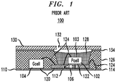
- FIG. 1 is a cross-sectional side view of a conventional semiconductor sensor device 100 having a pressure-sensing die (P-cell) 102 with an active surface 103, an acceleration-sensing die (G-cell) 104, and a micro controller unit (MCU) die 106 that processes pressure and acceleration signals generated by the P-cell 102 and G-cell 104, respectively.
- the device 100 is assembled using a metal (e.g., copper) lead frame 110, which includes a flag 112 and a plurality of leads 114.
- the G-cell 104 and the MCU 106 are mounted on the flag 112 (aka die paddle or die pad) using die attach film 120.
- the P-cell 102 is mounted or stacked on the MCU 106 using die attach adhesive 122.
- the P-cell 102 and the G-cell 104 are electrically connected to the MCU 106 and the MCU 106 is electrically connected to one or more of the leads 114 with respective bond wires 124.
- the G-cell 104, the bond wires 124 connecting the MCU 106 to the G-cell 104 and to the leads 114, and portions of the MCU 106 are encapsulated within a relatively rigid molding compound 126 that is applied using a film-assist molding (FAM) process, while the P-cell 102, the rest of the bond wires 124, and the remaining portions of the MCU 106 are covered by a relatively flexible pressure-sensitive gel 128.
- FAM film-assist molding
- a lid 130 which has a vent hole 132, is mounted on the molding compound 126 using lid adhesive 134.
- the vent hole 132 allows the ambient atmospheric pressure outside the sensor device 100 to reach the gel-covered P-cell 102.
- the molding compound 126, the gel 128, and the lid 130 protect the dies and the wire bonds from mechanical damage during packaging and environmental damage ( e.g ., contamination and/or corrosion) when in use.
- the gel 128 protects the bond wires 124 that connect the P-cell 102 to the MCU 106, while enabling the pressure-sensitive active region 103 on the top surface of the P-cell 102 to detect the ambient atmospheric pressure.
- One problem with the design of the sensor device 100 is the high manufacturing costs associated with the FAM process used to apply the molding compound 126, the gel-coating process used to apply the gel 128, and the lid-attach process used to attach the lid 130. Accordingly, it would be advantageous to have a more economical way to assemble semiconductor sensor devices.
- Embodiments of the present invention may be embodied in many alternative forms and should not be construed as limited to only the embodiments set forth herein. Further, the terminology used herein is for the purpose of describing particular embodiments only and is not intended to be limiting of example embodiments of the invention.
- semiconductor sensor devices such as packaged TPMS devices
- FAM film-assisted molding
- gel-coating gel-coating
- lid-attach processes can be performed without having to perform film-assisted molding (FAM), gel-coating, and lid-attach processes.
- the present invention is a semiconductor sensor device assembled using a lead frame that has a flag and a plurality of leads that surround the flag, and where the flag has a vent hole.
- An interposer is mounted on the lead frame flag and has a vent hole in fluid communication with the vent hole of the lead frame flag.
- a sensor die having an active region is mounted on and electrically connected to the interposer in a flip-chip manner such that the vent hole of the interposer is in fluid communication with the active region of the sensor die.
- Bond wires electrically connect the interposer to one or more other components of the device.
- a molding compound covers the sensor die, the interposer, and the bond wires.
- the present invention is a method for assembling a semiconductor sensor device.
- the method includes mounting an interposer having a vent hole on a lead frame flag having a vent hole such that the interposer vent hole is in fluid communication with the flag vent hole, and mounting on the interposer, in a flip-chip manner, a sensor die having an active region, such that the vent hole of the interposer is in fluid communication with the active region of the sensor die.
- Wire bonding is performed to electrically connect one or more other components of the device to the interpose using bond wires.
- a molding compound is used to encapsulate the sensor die, the interposer, and the bond wires.
- FIG. 2A is a cross- sectional side view (along the cut line X-X of FIG. 2B ) of a packaged semiconductor sensor device 200 in accordance with an embodiment of the invention
- FIG. 2B is a top view of the sensor device 200
- FIG. 2C is a bottom view of the sensor device 200 before molding.
- the sensor device 200 is assembled “upside down” and then turned over to the orientation shown in FIG. 2A .
- the configuration of the sensor device 200 is explained as follows.
- the sensor device 200 includes a P-Cell 202 having an active surface 203, a G-Cell 204, and a MCU 206, and is assembled using a lead frame 210 having a flag 212 having a hole 213 and a plurality of leads 214 that surround the flag 212.
- the lead frame 210 may be formed of copper, an alloy of copper, a copper-plated iron/nickel alloy, plated aluminum, or the like. Often, copper lead frames are pre-plated first with a nickel base layer, then a palladium mid-layer, and finally with a very thin, gold upper layer.
- the MCU 206 is mounted on the flag 212 with a DAF tape 220 or other suitable means for mounting a die to a substrate.
- An interposer 240 having a hole 241 also is mounted on the flag 212 with the DAF tape 220, but this portion of the DAF tape 220 includes a hole 221.
- the hole 221 is in fluid communication with the hole 213 in the flag 212 and the hole 241 in the interposer 240. Further, the holes 213, 221 and 241 are aligned over the active region 203 of the P-Cell 202, which allows the P-cell to sense the ambient pressure.
- the G-cell 204 is mounted on the MCU 206 using a suitable die-attach adhesive 222 (or other suitable means for mounting one die on another die), and the P-cell 202 is mounted on and electrically connected to the interposer 240 in a flip-chip manner using a suitable conductive die-attach epoxy 234 (or other suitable means for mounting and electrically connecting one die onto another die).
- a suitable die-attach adhesive 222 or other suitable means for mounting one die on another die
- the P-cell 202 is mounted on and electrically connected to the interposer 240 in a flip-chip manner using a suitable conductive die-attach epoxy 234 (or other suitable means for mounting and electrically connecting one die onto another die).
- Flip-chip bonding is a process known in the art for physically and electrically coupling die pads on a die, such as the P-cell 202, to the exposed ends of metal vias in a substrate, such as the interposer 240, where each of the die pads is substantially aligned with a corresponding metal via.
- controlled collapse chip connection (C4) metal bumps are first deposited by plating, jetting, stud bumping, direct placement (e.g., ball drop), or screen printing the bumps onto either the die pads or the metal vias. Then the die and the substrate are brought into close contact, and the metal bumps are bonded to both the die pads and the metal vias using heat, pressure, and ultrasonic vibration in a thermosonic process or heat and pressure in a reflow process.
- an interposer is an integrated electrical interface designed to spread a connection to a wider pitch or reroute a connection to a different connection.
- the interposer 240 provides one or more conductive interconnects 242 for electrically connecting the P-cell 202 to the MCU 206 with corresponding bond wires 224.
- the MCU 206 is electrically connected both to the G-cell 204 and to one or more leads 214 of the lead frame 210 with respective ones of the bond wires 224.
- the bond wires 224 are formed from a conductive material such as aluminum, silver, gold, or copper, and may be either coated or uncoated. All of these components of the sensor device 200 are encapsulated by a suitable molding compound 226.
- the molding compound 226 may be a plastic, an epoxy, a silica-filled resin, a ceramic, a halide-free material, the like, or a combination thereof, as known in the art.
- the MCU 206 functions as the controller for the sensor device 200 by, for example, controlling the operations of and processing of signals generated by the G-cell 204 and the P-cell 202.
- the P-cell 202, the G-cell 204, and the MCU 206 are well-known components used in semiconductor sensor devices and thus detailed descriptions thereof are not necessary for a complete understanding of the invention.
- the lead frame flag 212, the DAF tape 220, and the interposer 240 have corresponding vent holes 213, 221, and 241 that expose the (e.g., centrally located) pressure-sensitive active region 203 of the P-cell 202 to ambient atmospheric pressure outside the sensor device 200.
- the active region 203 is indicated by a broken circle because the active region 203 is on the other side of the P-cell 202 in that view.
- the lead frame flag 212 functions as the lid for the sensor device 200. As such, there is no need to mount a separate lid analogous to the lid 130 of the sensor device 100 of FIG. 1 .
- FIGS. 3A through 11B illustrate one possible process for assembling the sensor device 200 of FIGS. 2A-2C . Those skilled in the art will understand that other suitable manufacturing steps are possible.
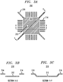
- FIG. 3A is a plan view of the lead frame 210 of FIGS. 2A-2C having the flag 212 with the vent hole 213 and surrounded on all four sides by leads 214 and supported by tie bars 216.
- leads 214 on all four sides of the flag 212, this is not a requirement, as one or more sides could have no, fewer or even more leads on that side.
- FIGS. 3B and 3C are cross-sectional side views of the lead frame 210 of FIG. 3A along the cut lines X-X and Y-Y, respectively.
- FIGS. 3B and 3C illustrate the down-set of the flag 212 relative to the leads 214 and the tie bars 216. Note that, for purposes of simplification, the tie bars 216 are not represented in any of the other figures.
- the lead frame 210 of FIGS. 3A-3C is one of many similar lead frames in a two- dimensional lead frame array, such that multiple instances of the sensor device 200 are made in parallel.
- the other lead frames in the array are not shown in any of the figures.
- FIG. 4A is a plan view of a sub-assembly 400 that includes the interposer 240 having the vent hole 241.
- FIG. 4B is a cross-sectional side view (along cut line Y-Y of FIG. 4A ) of the sub-assembly 400 showing the DAF tape 220 having the vent hole 221.
- Internal interconnects 242 within the interposer 240 have inner pads 402 and outer pads 404 on the top surface of the interposer 240, where, the inner pads 402 are electrically mated with corresponding pads (not labeled) on the P-cell 202 and the outer pads 404 are electrically mated to corresponding bond wires 224.
- FIG. 5 is a plan view of a sub-assembly 500 that is produced by mounting the sub-assembly 400 of FIG. 4B on the lead frame flag 212 of FIGS. 3A-3C with the vent holes 213, 221, and 241 co-aligned to provide fluid communication between them.
- FIG. 6 is a plan view of a sub-assembly 600 that is produced by applying the conductive die-attach epoxy 234 on the interposer 240 of the sub-assembly 500 of FIG. 5 using a suitable stamping and printing process. Note that, in addition to being applied in a ring 602 around the interposer vent hole 241, the die-attach epoxy 234 also is applied to each of the inner pads 402 of the interposer 240, where the epoxy 234 on each inner pad 402 is electrically isolated from the epoxy 234 on each other inner pad 402 as well as from the ring 602 of epoxy 234 around the vent hole 241.
- FIG. 7 is a plan view of a sub-assembly 700 that is produced by mounting the P-cell 202 in a flip-chip manner onto the interposer 240 of the sub-assembly 600 of FIG. 6 , with the pressure-sensitive active region 203 of the P-cell 202 co- aligned with the vent holes 213, 221, and 241 to provide fluid communication between them to enable the P-cell 202 to sense ambient atmospheric pressure outside of the sensor device 200.
- FIG. 8 is a plan view of a sub-assembly 800 that is produced by (i) mounting the MCU 206 on the lead frame flag 212 of the sub-assembly 700 of FIG. 7 and (ii) mounting the G-cell 204 on the MCU 206.
- the G-cell 204 can be mounted on the MCU 206 either before or after the MCU 206 is mounted on the flag 212.
- FIGS. 5-8 can be implemented in a different order.
- the MCU 206 and the G-cell 204 can be mounted before the interposer 240 and the P-cell 202 are mounted.
- Other sequences also are possible.
- FIG. 9 is a plan view of a sub-assembly 900 that is produced by wire bonding the subassembly 800 of FIG. 8 .
- the MCU 206 is electrically connected to the G-cell 204, the P-cell 202, and the corresponding lead frame leads 214 with bond wires 224 and
- the G-cell 204 is electrically connected to the MCU 206 with the corresponding bond wires 224.
- FIG. 10 is a plan view of a sub-assembly 1000 produced by applying the molding compound 226 on the sub- assembly 900 of FIG. 9 . Note that the molding compound 226 is applied over all the exposed components on the top side of the sub-assembly 900. As such, an expensive film-assist molding (FAM) process does not need to be performed.
- FAM film-assist molding
- FIG. 11A is a plan view of an assembly 1100 and FIG. 11B is a cross-sectional side view of the assembly 1100 along the cut line P-P that is produced by (i) performing singulation using a stamp, saw, laser or combination thereof on the two-dimensional array of multiple instances of the sub- assembly 1000 of FIG. 10 and (ii) performing a trim and form process including bending the leads 214 into reverse gull-wing shapes, as shown in FIG. 11B .
- the assembly 1100 is equivalent to the sensor device 200 of FIG. 2A in an upside- down orientation.
- the sensor device 200 is shown without any pressure-sensitive gel similar to the gel 128 of FIG. 1 . If appropriate, however, after turning over the sub-assembly 1100 of FIG. 11B , a pressure-sensitive gel can be applied through the vent holes 213, 221, and 241 onto the exposed surface of the P-cell 202 of FIG. 2A .
- the gel material may be dispensed through the holes 213, 221, and 241 with a nozzle of a conventional dispensing machine as is known in the art.
- the G-cell 204 can be mounted on and electrically connected to the MCU 206 in a flip-chip manner without requiring bond wires or the G-cell 204 can be mounted directly on the lead frame flag 212 adjacent to the MCU 206 and electrically connected to the MCU 206 using bond wires.
- the G-cell 204 may be omitted.
- the acceleration-sensing function of the G-cell 204 may be implemented by the MCU 206, by the P-cell 202, or not at all (for sensor-device applications that do not require acceleration sensing). Note further that some embodiments may have one or more other dies (not shown) mounted, for example, onto the MCU 206 or onto the flag 212 adjacent to the MCU 206.
- the invention has been described in the context of the pressure-sensing sensor device 200 having a P- cell 202 with a pressure-sensitive active region 203, those skilled in the art will understand that, in alternative embodiments, the invention can be implemented in the context of other types of sensor devices having other types of sensor dies with active regions that are designed to detect features other than pressure, such as, without limitation, temperature, radiation (including visible light), or specific chemical compounds.
- the term “mounted onto” as in “a die mounted onto a lead frame flag” covers situations in which the die is mounted directly onto the flag with no other intervening dies or other structures except an adhesive layer as well as situations in which the die is directly mounted onto another die, which is itself mounted directly onto the flag. Note that “mounted onto” also covers situations in which there are two or more intervening structures between the die and flag. Depending on the situation, the term “mounted” can imply electrical connection in addition to physical attachment, where the electrical connection may be provided by one or more bond wires, one or more metal bumps, and/or any other suitable technique.
- no-leads type packages such as quad flat no-leads (QFN) packages, ball grid array (BGA) packages, molded array packages (MAP), quad flat pack (QFP) packages, and small-outline (SO) packages.
- QFN quad flat no-leads
- BGA ball grid array
- MAP molded array packages
- QFP quad flat pack
- SO small-outline
- a lead frame is a collection of metal leads and possibly other elements (e.g., die flags and power bars) that is used in semiconductor packaging for assembling one or more integrated circuit (IC) dies into a single packaged semiconductor device.
- a lead frame Prior to assembly into a packaged device, a lead frame may have support structures (e.g., a rectangular metal frame and tie bars) that keep those elements in place. During the assembly process, the support structures may be removed.
- the term "lead frame” may be used to refer to the collection of elements before assembly or after assembly, regardless of the presence or absence of those support structures.
Landscapes
- Engineering & Computer Science (AREA)
- Microelectronics & Electronic Packaging (AREA)
- Manufacturing & Machinery (AREA)
- Physics & Mathematics (AREA)
- General Physics & Mathematics (AREA)
- Computer Hardware Design (AREA)
- Chemical & Material Sciences (AREA)
- Analytical Chemistry (AREA)
- Pressure Sensors (AREA)
- Encapsulation Of And Coatings For Semiconductor Or Solid State Devices (AREA)
- Measuring Fluid Pressure (AREA)
Abstract
A semiconductor sensor device includes a lead frame flag having a vent hole, an interposer mounted on the flag and having a vent hole in fluid communication with the vent hole of the flag, and a sensor die having an active region. The sensor die is mounted on and electrically connected to the interposer in a flip-chip manner such that the vent hole of the interposer is in fluid communication with the active region of the sensor die. Bond wires electrically connect the interposer to one or more other components of the device. A molding compound covers the sensor die, the interposer, and the bond wires. The sensor die may be a pressure-sensing (P- cell) die, and the device may also include a microcontroller unit (MCU) die and an acceleration-sensing (G-cell) die, for tire pressure monitoring applications.
Description
- The present invention relates generally to semiconductor sensor devices and, more particularly, to semiconductor sensor devices for tire-pressure monitoring systems (TPMS).
- Semiconductor sensor devices, such as packaged TPMS pressure sensors, are well known. Each such device contains a pressure-sensing semiconductor die (aka P-cell), such as a piezo-resistive transducer or a parameterized layout cell, having an active, pressure-sensitive region on the top surface of the die. Such a P-cell does not allow full encapsulation in conventional molding compound, because that would prevent ambient atmospheric pressure from reaching the active region, thereby impeding the P-cell's functionality.
-
FIG. 1 is a cross-sectional side view of a conventionalsemiconductor sensor device 100 having a pressure-sensing die (P-cell) 102 with anactive surface 103, an acceleration-sensing die (G-cell) 104, and a micro controller unit (MCU) die 106 that processes pressure and acceleration signals generated by the P-cell 102 and G-cell 104, respectively. Thedevice 100 is assembled using a metal (e.g., copper)lead frame 110, which includes aflag 112 and a plurality ofleads 114. The G-cell 104 and the MCU 106 are mounted on the flag 112 (aka die paddle or die pad) using dieattach film 120. The P-cell 102 is mounted or stacked on theMCU 106 using die attach adhesive 122. The P-cell 102 and the G-cell 104 are electrically connected to theMCU 106 and theMCU 106 is electrically connected to one or more of theleads 114 withrespective bond wires 124. - The G-
cell 104, thebond wires 124 connecting theMCU 106 to the G-cell 104 and to theleads 114, and portions of theMCU 106 are encapsulated within a relativelyrigid molding compound 126 that is applied using a film-assist molding (FAM) process, while the P-cell 102, the rest of thebond wires 124, and the remaining portions of theMCU 106 are covered by a relatively flexible pressure-sensitive gel 128. - A
lid 130, which has avent hole 132, is mounted on themolding compound 126 using lid adhesive 134. Thevent hole 132 allows the ambient atmospheric pressure outside thesensor device 100 to reach the gel-covered P-cell 102. Themolding compound 126, thegel 128, and thelid 130 protect the dies and the wire bonds from mechanical damage during packaging and environmental damage (e.g., contamination and/or corrosion) when in use. Thegel 128 protects thebond wires 124 that connect the P-cell 102 to theMCU 106, while enabling the pressure-sensitiveactive region 103 on the top surface of the P-cell 102 to detect the ambient atmospheric pressure. - One problem with the design of the
sensor device 100 is the high manufacturing costs associated with the FAM process used to apply themolding compound 126, the gel-coating process used to apply thegel 128, and the lid-attach process used to attach thelid 130. Accordingly, it would be advantageous to have a more economical way to assemble semiconductor sensor devices. - Embodiments of the present invention are illustrated by way of example and are not limited by the accompanying figures, in which like references indicate similar elements. Elements in the figures are illustrated for simplicity and clarity and have not necessarily been drawn to scale. For example, the thicknesses of layers and regions may be exaggerated for clarity.
-
FIG. 1 is a cross-sectional side view of a conventional packaged semiconductor sensor device; -
FIG. 2A is a cross-sectional side view (along the cut line X-X ofFIG. 2B ) of a packaged semiconductor sensor device in accordance with an embodiment of the present invention, -
FIG. 2B is a top plan view of the sensor device ofFIG. 2A , and -
FIG. 2C is a bottom view of the sensor device ofFIG. 2A before molding; -
FIG. 3A is a plan view of a lead frame of the sensor device ofFIG. 2A , and -
FIGS. 3B and 3C are sectional views of the lead frame ofFIG. 3A along lines X-X and Y-Y, respectively; -
FIG. 4A is a plan view of a sub-assembly that includes an interposer and DAF tape of the device ofFIG. 2A , and -
FIG. 4B is a cross-sectional side view along line Y-Y ofFIG. 4A of the subassembly ofFIG. 4A ; -
FIG. 5 is a plan view of a sub-assembly that is produced by mounting the sub-assembly ofFIG. 4B on a lead frame flag ofFIG. 3A ; -
FIG. 6 is a plan view of a sub-assembly that is produced by applying a conductive die-attach epoxy of the device ofFIG. 2A on an interposer of the sub-assembly ofFIG. 5 ; -
FIG. 7 is a plan view of a sub-assembly that is produced by mounting a P-cell of the device ofFIG. 2A in a flip-chip manner on the interposer of the sub-assembly ofFIG. 6 ; -
FIG. 8 is a plan view of a sub-assembly that is produced by (i) mounting an MCU of the device ofFIG. 2A on a lead frame flag of the sub-assembly ofFIG. 7 and (ii) mounting a G-cell of the device ofFIG. 2A on the MCU of the device ofFIG. 2A ; -
FIG. 9 is a plan view of a sub-assembly that is produced after performing wire bonding on the sub-assembly ofFIG. 8 ; -
FIG. 10 is a plan view of a sub-assembly that is produced by applying a molding compound on the sub-assembly ofFIG. 9 ; -
FIG. 11A is a plan view of an assembly that is produced performing singulation and trim and form processes on the sub-assembly ofFIG. 10 ; and -
FIG. 11B is a cross-sectional side view of the assembly ofFIG. 11A along cut line P-P. - Detailed illustrative embodiments of the present invention are disclosed herein. However, specific structural and functional details disclosed herein are merely representative for purposes of describing example embodiments of the present invention.
- Embodiments of the present invention may be embodied in many alternative forms and should not be construed as limited to only the embodiments set forth herein. Further, the terminology used herein is for the purpose of describing particular embodiments only and is not intended to be limiting of example embodiments of the invention.
- As used herein, the singular forms "a", "an", and "the", are intended to include the plural forms as well, unless the context clearly indicates otherwise. It further will be understood that the terms "comprises", "comprising", "has", "having", "includes", or "including" specify the presence of stated features, steps, or components, but do not preclude the presence or addition of one or more other features, steps, or components. It also should be noted that, in some alternative implementations, the functions/ acts noted might occur out of the order noted in the figures. For example, two figures shown in succession may in fact be executed substantially concurrently or may sometimes be executed in the reverse order, depending upon the functionality/acts involved. The term "or" is to be interpreted as inclusive unless indicated otherwise.
- According to embodiments of the present invention, semiconductor sensor devices, such as packaged TPMS devices, can be assembled without having to perform film-assisted molding (FAM), gel-coating, and lid-attach processes.
- In one embodiment, the present invention is a semiconductor sensor device assembled using a lead frame that has a flag and a plurality of leads that surround the flag, and where the flag has a vent hole. An interposer is mounted on the lead frame flag and has a vent hole in fluid communication with the vent hole of the lead frame flag.A sensor die having an active region is mounted on and electrically connected to the interposer in a flip-chip manner such that the vent hole of the interposer is in fluid communication with the active region of the sensor die. Bond wires electrically connect the interposer to one or more other components of the device. A molding compound covers the sensor die, the interposer, and the bond wires.
- In another embodiment, the present invention is a method for assembling a semiconductor sensor device. The method includes mounting an interposer having a vent hole on a lead frame flag having a vent hole such that the interposer vent hole is in fluid communication with the flag vent hole, and mounting on the interposer, in a flip-chip manner, a sensor die having an active region, such that the vent hole of the interposer is in fluid communication with the active region of the sensor die. Wire bonding is performed to electrically connect one or more other components of the device to the interpose using bond wires. A molding compound is used to encapsulate the sensor die, the interposer, and the bond wires.
- Referring now to
FIGS. 2A-2C, FIG. 2A is a cross- sectional side view (along the cut line X-X ofFIG. 2B ) of a packaged semiconductor sensor device 200 in accordance with an embodiment of the invention,FIG. 2B is a top view of the sensor device 200, andFIG. 2C is a bottom view of the sensor device 200 before molding. As explained in further detail below, the sensor device 200 is assembled "upside down" and then turned over to the orientation shown inFIG. 2A . With that understanding, the configuration of the sensor device 200 is explained as follows. - The sensor device 200 includes a P-
Cell 202 having anactive surface 203, a G-Cell 204, and aMCU 206, and is assembled using alead frame 210 having aflag 212 having ahole 213 and a plurality ofleads 214 that surround theflag 212. Thelead frame 210 may be formed of copper, an alloy of copper, a copper-plated iron/nickel alloy, plated aluminum, or the like. Often, copper lead frames are pre-plated first with a nickel base layer, then a palladium mid-layer, and finally with a very thin, gold upper layer. - The
MCU 206 is mounted on theflag 212 with aDAF tape 220 or other suitable means for mounting a die to a substrate. Aninterposer 240 having ahole 241 also is mounted on theflag 212 with theDAF tape 220, but this portion of theDAF tape 220 includes ahole 221. Thehole 221 is in fluid communication with thehole 213 in theflag 212 and thehole 241 in theinterposer 240. Further, theholes active region 203 of the P-Cell 202, which allows the P-cell to sense the ambient pressure. - The G-
cell 204 is mounted on theMCU 206 using a suitable die-attach adhesive 222 (or other suitable means for mounting one die on another die), and the P-cell 202 is mounted on and electrically connected to theinterposer 240 in a flip-chip manner using a suitable conductive die-attach epoxy 234 (or other suitable means for mounting and electrically connecting one die onto another die). - Flip-chip bonding is a process known in the art for physically and electrically coupling die pads on a die, such as the P-
cell 202, to the exposed ends of metal vias in a substrate, such as theinterposer 240, where each of the die pads is substantially aligned with a corresponding metal via. In a typical BGA (ball grid array) flip-chip process, controlled collapse chip connection (C4) metal bumps are first deposited by plating, jetting, stud bumping, direct placement (e.g., ball drop), or screen printing the bumps onto either the die pads or the metal vias. Then the die and the substrate are brought into close contact, and the metal bumps are bonded to both the die pads and the metal vias using heat, pressure, and ultrasonic vibration in a thermosonic process or heat and pressure in a reflow process. - As known in the art, an interposer is an integrated electrical interface designed to spread a connection to a wider pitch or reroute a connection to a different connection. In the sensor device 200, the
interposer 240 provides one or moreconductive interconnects 242 for electrically connecting the P-cell 202 to theMCU 206 withcorresponding bond wires 224. In addition, theMCU 206 is electrically connected both to the G-cell 204 and to one or more leads 214 of thelead frame 210 with respective ones of thebond wires 224. Thebond wires 224 are formed from a conductive material such as aluminum, silver, gold, or copper, and may be either coated or uncoated. All of these components of the sensor device 200 are encapsulated by asuitable molding compound 226. Themolding compound 226 may be a plastic, an epoxy, a silica-filled resin, a ceramic, a halide-free material, the like, or a combination thereof, as known in the art. - The
MCU 206 functions as the controller for the sensor device 200 by, for example, controlling the operations of and processing of signals generated by the G-cell 204 and the P-cell 202. The P-cell 202, the G-cell 204, and theMCU 206 are well-known components used in semiconductor sensor devices and thus detailed descriptions thereof are not necessary for a complete understanding of the invention. - As represented in
FIGS. 2A-2C , thelead frame flag 212, theDAF tape 220, and theinterposer 240 have corresponding vent holes 213, 221, and 241 that expose the (e.g., centrally located) pressure-sensitiveactive region 203 of the P-cell 202 to ambient atmospheric pressure outside the sensor device 200. Note that, inFIG. 2C , theactive region 203 is indicated by a broken circle because theactive region 203 is on the other side of the P-cell 202 in that view. - As represented in
FIG. 2A , thelead frame flag 212 functions as the lid for the sensor device 200. As such, there is no need to mount a separate lid analogous to thelid 130 of thesensor device 100 ofFIG. 1 . - Furthermore, as explained below, since the
molding compound 226 is applied over all the exposed components, there is no need to employ an expensive film-assist molding (FAM) process when applying themolding compound 226. - Lastly, unlike the
sensor device 100 ofFIG. 1 , since all thebond wires 224 are encapsulated in themolding compound 226, an expensive pressure-sensitive gel analogous to the pressure-sensitive gel 128 ofFIG. 1 is not needed to protect any bond wires. Note that the option still exists to apply a pressure-sensitive gel over the exposedactive surface 203 of the P-cell 202, for example, to protect the P-cell 202 from environmental damage. -
FIGS. 3A through 11B illustrate one possible process for assembling the sensor device 200 ofFIGS. 2A-2C . Those skilled in the art will understand that other suitable manufacturing steps are possible. -
FIG. 3A is a plan view of thelead frame 210 ofFIGS. 2A-2C having theflag 212 with thevent hole 213 and surrounded on all four sides byleads 214 and supported by tie bars 216. Although the embodiment has leads 214 on all four sides of theflag 212, this is not a requirement, as one or more sides could have no, fewer or even more leads on that side. -
FIGS. 3B and 3C are cross-sectional side views of thelead frame 210 ofFIG. 3A along the cut lines X-X and Y-Y, respectively.FIGS. 3B and 3C illustrate the down-set of theflag 212 relative to theleads 214 and the tie bars 216. Note that, for purposes of simplification, the tie bars 216 are not represented in any of the other figures. - In a preferred assembly process, the
lead frame 210 ofFIGS. 3A-3C is one of many similar lead frames in a two- dimensional lead frame array, such that multiple instances of the sensor device 200 are made in parallel. For purposes of simplification, the other lead frames in the array are not shown in any of the figures. -
FIG. 4A is a plan view of a sub-assembly 400 that includes theinterposer 240 having thevent hole 241.FIG. 4B is a cross-sectional side view (along cut line Y-Y ofFIG. 4A ) of the sub-assembly 400 showing theDAF tape 220 having thevent hole 221. Internal interconnects 242 within theinterposer 240 haveinner pads 402 andouter pads 404 on the top surface of theinterposer 240, where, theinner pads 402 are electrically mated with corresponding pads (not labeled) on the P-cell 202 and theouter pads 404 are electrically mated to correspondingbond wires 224. -
FIG. 5 is a plan view of a sub-assembly 500 that is produced by mounting thesub-assembly 400 ofFIG. 4B on thelead frame flag 212 ofFIGS. 3A-3C with the vent holes 213, 221, and 241 co-aligned to provide fluid communication between them. -
FIG. 6 is a plan view of a sub-assembly 600 that is produced by applying the conductive die-attachepoxy 234 on theinterposer 240 of the sub-assembly 500 ofFIG. 5 using a suitable stamping and printing process. Note that, in addition to being applied in aring 602 around theinterposer vent hole 241, the die-attachepoxy 234 also is applied to each of theinner pads 402 of theinterposer 240, where the epoxy 234 on eachinner pad 402 is electrically isolated from the epoxy 234 on each otherinner pad 402 as well as from thering 602 ofepoxy 234 around thevent hole 241. -
FIG. 7 is a plan view of a sub-assembly 700 that is produced by mounting the P-cell 202 in a flip-chip manner onto theinterposer 240 of the sub-assembly 600 ofFIG. 6 , with the pressure-sensitiveactive region 203 of the P-cell 202 co- aligned with the vent holes 213, 221, and 241 to provide fluid communication between them to enable the P-cell 202 to sense ambient atmospheric pressure outside of the sensor device 200. -
FIG. 8 is a plan view of a sub-assembly 800 that is produced by (i) mounting theMCU 206 on thelead frame flag 212 of the sub-assembly 700 ofFIG. 7 and (ii) mounting the G-cell 204 on theMCU 206. Note that, depending on the particular implementation, the G-cell 204 can be mounted on theMCU 206 either before or after theMCU 206 is mounted on theflag 212. - Note further that the steps represented by
FIGS. 5-8 can be implemented in a different order. For example, theMCU 206 and the G-cell 204 can be mounted before theinterposer 240 and the P-cell 202 are mounted. Other sequences also are possible. -
FIG. 9 is a plan view of a sub-assembly 900 that is produced by wire bonding the subassembly 800 ofFIG. 8 . In particular, (i) theMCU 206 is electrically connected to the G-cell 204, the P-cell 202, and the corresponding lead frame leads 214 withbond wires 224 and (ii) the G-cell 204 is electrically connected to theMCU 206 with thecorresponding bond wires 224. -
FIG. 10 is a plan view of a sub-assembly 1000 produced by applying themolding compound 226 on the sub-assembly 900 ofFIG. 9 . Note that themolding compound 226 is applied over all the exposed components on the top side of thesub-assembly 900. As such, an expensive film-assist molding (FAM) process does not need to be performed. -
FIG. 11A is a plan view of anassembly 1100 andFIG. 11B is a cross-sectional side view of theassembly 1100 along the cut line P-P that is produced by (i) performing singulation using a stamp, saw, laser or combination thereof on the two-dimensional array of multiple instances of the sub-assembly 1000 ofFIG. 10 and (ii) performing a trim and form process including bending theleads 214 into reverse gull-wing shapes, as shown inFIG. 11B . Note that theassembly 1100 is equivalent to the sensor device 200 ofFIG. 2A in an upside- down orientation. - As represented in
FIG. 2A and unlike in the prior-art sensor device 100 ofFIG. 1 , all thebond wires 224 are encapsulated within themolding compound 226. As such, as represented inFIG. 2A , the sensor device 200 is shown without any pressure-sensitive gel similar to thegel 128 ofFIG. 1 . If appropriate, however, after turning over thesub-assembly 1100 ofFIG. 11B , a pressure-sensitive gel can be applied through the vent holes 213, 221, and 241 onto the exposed surface of the P-cell 202 ofFIG. 2A . The gel material may be dispensed through theholes epoxy 234 to connect theinner pads 402 on theinterposer 240 to corresponding pads on the P-cell 202, a suitable ball-grid array on either theinterposer 240 or the P-cell 202 can be employed. - Although the invention has been described in the context of the sensor device 200 having the G-
cell 204 mounted on and wire-bonded to theMCU 206, in alternative embodiments, the G-cell 204 can be mounted on and electrically connected to theMCU 206 in a flip-chip manner without requiring bond wires or the G-cell 204 can be mounted directly on thelead frame flag 212 adjacent to theMCU 206 and electrically connected to theMCU 206 using bond wires. In other alternative embodiments, the G-cell 204 may be omitted. In some embodiments, the acceleration-sensing function of the G-cell 204 may be implemented by theMCU 206, by the P-cell 202, or not at all (for sensor-device applications that do not require acceleration sensing). Note further that some embodiments may have one or more other dies (not shown) mounted, for example, onto theMCU 206 or onto theflag 212 adjacent to theMCU 206. - Although the invention has been described in the context of the pressure-sensing sensor device 200 having a P-
cell 202 with a pressure-sensitiveactive region 203, those skilled in the art will understand that, in alternative embodiments, the invention can be implemented in the context of other types of sensor devices having other types of sensor dies with active regions that are designed to detect features other than pressure, such as, without limitation, temperature, radiation (including visible light), or specific chemical compounds. - As used herein, the term "mounted onto" as in "a die mounted onto a lead frame flag" covers situations in which the die is mounted directly onto the flag with no other intervening dies or other structures except an adhesive layer as well as situations in which the die is directly mounted onto another die, which is itself mounted directly onto the flag. Note that "mounted onto" also covers situations in which there are two or more intervening structures between the die and flag. Depending on the situation, the term "mounted" can imply electrical connection in addition to physical attachment, where the electrical connection may be provided by one or more bond wires, one or more metal bumps, and/or any other suitable technique.
- Those skilled in the art will understand that the invention can be implemented in a variety of different types of packages including (without limitation) no-leads type packages such as quad flat no-leads (QFN) packages, ball grid array (BGA) packages, molded array packages (MAP), quad flat pack (QFP) packages, and small-outline (SO) packages.
- A lead frame is a collection of metal leads and possibly other elements (e.g., die flags and power bars) that is used in semiconductor packaging for assembling one or more integrated circuit (IC) dies into a single packaged semiconductor device. Prior to assembly into a packaged device, a lead frame may have support structures (e.g., a rectangular metal frame and tie bars) that keep those elements in place. During the assembly process, the support structures may be removed. As used herein, the term "lead frame" may be used to refer to the collection of elements before assembly or after assembly, regardless of the presence or absence of those support structures.
- Although the invention is described herein with reference to specific embodiments, various modifications and changes can be made without departing from the scope of the present invention as set forth in the claims below.
- Accordingly, the specification and figures are to be regarded in an illustrative rather than a restrictive sense, and all such modifications are intended to be included within the scope of the present invention. Any benefits, advantages, or solutions to problems that are described herein with regard to specific embodiments are not intended to be construed as a critical, required, or essential feature or element of any or all the claims.
Claims (15)
- A semiconductor sensor device, comprising: a lead frame flag having a vent hole;an interposer mounted on the lead frame flag and having a vent hole in fluid communication with the vent hole of the lead frame flag;a sensor die having an active region, wherein the sensor die is mounted on and electrically connected to the interposer in a flip-chip manner such that the vent hole of the interposer is in fluid communication with the active region of the sensor die;bond wires electrically connecting the interposer to one or more other components of the device; andmolding compound encapsulating the sensor die, the interposer, and the bond wires.
- The device of claim 1, wherein the sensor die is a pressure-sensing die having a pressure-sensitive active region, and wherein the vent hole of the interposer is in fluid communication with the active region of the pressure- sensing die to enable the pressure-sensing die to sense ambient atmospheric pressure outside of the device.
- The device of claim 1 or 2, wherein the vent holes of the lead frame flag and the interposer are aligned with each other and with the active region of the sensor die.
- The device of any preceding claim, further comprising a micro control unit (MCU) die mounted on the lead frame flag, and electrically connected to the interposer with one or more of the bond wires, and wherein the MCU die is covered by the molding compound.
- The device of claim 4, further comprising an acceleration-sensing die electrically connected to the MCU die and covered by the molding compound.
- The device of any preceding claim, wherein the lead frame flag functions as a lid for the device.
- The device of any preceding claim, wherein all the bond wires in the device are covered by the molding compound.
- The device of any preceding claim, wherein the active region of the sensor die is not covered by a pressure-sensitive gel.
- A method of assembling a semiconductor sensor device, the method comprising:mounting an interposer having a vent hole on a lead frame flag having a vent hole such that the interposer vent hole is in fluid communication with the lead frame flag vent hole;mounting a sensor die on the interposer in a flip-chip manner, wherein the sensor die has an active region, and wherein the vent hole of the interposer is in fluid communication with the active region of the sensor die;electrically connecting the interposer to one or more other components of the device using bond wires; andapplying molding compound to encapsulate the sensor die, the interposer, and the bond wires.
- The method of claim 9, wherein the sensor die is a pressure-sensing die having a pressure-sensitive active region, and the vent hole of the interposer is in fluid communication with the active region of the pressure-sensing die to enable the pressure-sensing die to sense ambient atmospheric pressure outside of the device.
- The method of claim 9 or 10, wherein the vent holes of the lead frame flag and the interposer are aligned with each other and with the active region of the sensor die.
- The method of any of claims 9 to 11, further comprising: mounting an MCU die on the
lead frame flag;
electrically connecting the MCU die to the interposer;
and
covering the MCU die with the molding compound. - The method of claim 12, further comprising electrically connecting an acceleration-sensing die to the MCU die, wherein the acceleration-sensing die is covered by the molding compound.
- The method of any of claims 9 to 13, wherein the lead frame flag functions as a lid for the device.
- The method of any of claims 9 to 14, wherein all the bond wires of the device are covered by the molding compound.
Applications Claiming Priority (1)
| Application Number | Priority Date | Filing Date | Title |
|---|---|---|---|
| US16/174,296 US10787361B2 (en) | 2018-10-30 | 2018-10-30 | Sensor device with flip-chip die and interposer |
Publications (1)
| Publication Number | Publication Date |
|---|---|
| EP3647755A1 true EP3647755A1 (en) | 2020-05-06 |
Family
ID=68295959
Family Applications (1)
| Application Number | Title | Priority Date | Filing Date |
|---|---|---|---|
| EP19203327.2A Withdrawn EP3647755A1 (en) | 2018-10-30 | 2019-10-15 | Sensor device with flip-chip die and interposer |
Country Status (2)
| Country | Link |
|---|---|
| US (1) | US10787361B2 (en) |
| EP (1) | EP3647755A1 (en) |
Families Citing this family (3)
| Publication number | Priority date | Publication date | Assignee | Title |
|---|---|---|---|---|
| US11225409B2 (en) | 2018-09-17 | 2022-01-18 | Invensense, Inc. | Sensor with integrated heater |
| US20220221353A1 (en) * | 2021-01-12 | 2022-07-14 | Texas Instruments Incorporated | Semiconductor force sensors |
| DE102021113914A1 (en) | 2021-05-28 | 2022-12-01 | Endress+Hauser SE+Co. KG | Measuring device for determining and/or monitoring at least one physical and/or chemical parameter |
Citations (2)
| Publication number | Priority date | Publication date | Assignee | Title |
|---|---|---|---|---|
| US20150054099A1 (en) * | 2013-08-25 | 2015-02-26 | Kai Yun Yow | Pressure sensor device and assembly method |
| US20160084722A1 (en) * | 2014-09-24 | 2016-03-24 | Freescale Semiconductor Inc. | Differential Pressure Sensor Assembly |
Family Cites Families (10)
| Publication number | Priority date | Publication date | Assignee | Title |
|---|---|---|---|---|
| US6661084B1 (en) | 2000-05-16 | 2003-12-09 | Sandia Corporation | Single level microelectronic device package with an integral window |
| TWI285415B (en) | 2005-08-01 | 2007-08-11 | Advanced Semiconductor Eng | Package structure having recession portion on the surface thereof and method of making the same |
| US9040352B2 (en) | 2012-06-28 | 2015-05-26 | Freescale Semiconductor, Inc. | Film-assist molded gel-fill cavity package with overflow reservoir |
| US8946833B2 (en) | 2012-10-22 | 2015-02-03 | Freescale Semiconductor, Inc. | Packaging for semiconductor sensor devices and methods |
| WO2014066768A2 (en) | 2012-10-25 | 2014-05-01 | Robert Bosch Gmbh | Combined pressure and humidity sensor |
| US20150069537A1 (en) * | 2013-09-08 | 2015-03-12 | Wai Yew Lo | Package-on-package semiconductor sensor device |
| US10103128B2 (en) * | 2013-10-04 | 2018-10-16 | Mediatek Inc. | Semiconductor package incorporating redistribution layer interposer |
| US9362479B2 (en) | 2014-07-22 | 2016-06-07 | Freescale Semiconductor, Inc. | Package-in-package semiconductor sensor device |
| EP3211394B1 (en) * | 2016-02-29 | 2021-03-31 | Melexis Technologies NV | Semiconductor pressure sensor for harsh media application |
| US10483191B2 (en) * | 2016-07-15 | 2019-11-19 | Stmicroelectronics, Inc. | Bottom package exposed die MEMS pressure sensor integrated circuit package design |
-
2018
- 2018-10-30 US US16/174,296 patent/US10787361B2/en not_active Expired - Fee Related
-
2019
- 2019-10-15 EP EP19203327.2A patent/EP3647755A1/en not_active Withdrawn
Patent Citations (2)
| Publication number | Priority date | Publication date | Assignee | Title |
|---|---|---|---|---|
| US20150054099A1 (en) * | 2013-08-25 | 2015-02-26 | Kai Yun Yow | Pressure sensor device and assembly method |
| US20160084722A1 (en) * | 2014-09-24 | 2016-03-24 | Freescale Semiconductor Inc. | Differential Pressure Sensor Assembly |
Also Published As
| Publication number | Publication date |
|---|---|
| US10787361B2 (en) | 2020-09-29 |
| US20200131026A1 (en) | 2020-04-30 |
Similar Documents
| Publication | Publication Date | Title |
|---|---|---|
| US8802474B1 (en) | Pressure sensor and method of packaging same | |
| US20140374848A1 (en) | Semiconductor sensor device with metal lid | |
| US8378435B2 (en) | Pressure sensor and method of assembling same | |
| US8836101B2 (en) | Multi-chip semiconductor packages and assembly thereof | |
| US8178961B2 (en) | Semiconductor package structure and package process | |
| US20150069537A1 (en) | Package-on-package semiconductor sensor device | |
| US20120139067A1 (en) | Pressure sensor and method of packaging same | |
| US9362479B2 (en) | Package-in-package semiconductor sensor device | |
| US9297713B2 (en) | Pressure sensor device with through silicon via | |
| US9040335B2 (en) | Side vented pressure sensor device | |
| US11355423B2 (en) | Bottom package exposed die MEMS pressure sensor integrated circuit package design | |
| US7642638B2 (en) | Inverted lead frame in substrate | |
| US9890034B2 (en) | Cavity type pressure sensor device | |
| US20150014793A1 (en) | Pressure sensor having down-set flag | |
| US10787361B2 (en) | Sensor device with flip-chip die and interposer | |
| US20150054099A1 (en) | Pressure sensor device and assembly method | |
| US20150160087A1 (en) | Stacked die sensor package | |
| US11276615B2 (en) | Semiconductor device package with a cap to selectively exclude contact with mold compound | |
| US5963782A (en) | Semiconductor component and method of manufacture | |
| US20170081178A1 (en) | Semiconductor device package with seal structure | |
| US20170110339A1 (en) | Ic device having patterned, non-conductive substrate | |
| US9638596B2 (en) | Cavity-down pressure sensor device | |
| NL2027540B1 (en) | Semiconductor Lead-on-Chip Assembly | |
| KR19990081577A (en) | Multi-chip package | |
| KR19990058160A (en) | BG package and manufacturing method thereof |
Legal Events
| Date | Code | Title | Description |
|---|---|---|---|
| PUAI | Public reference made under article 153(3) epc to a published international application that has entered the european phase |
Free format text: ORIGINAL CODE: 0009012 |
|
| STAA | Information on the status of an ep patent application or granted ep patent |
Free format text: STATUS: THE APPLICATION HAS BEEN PUBLISHED |
|
| AK | Designated contracting states |
Kind code of ref document: A1 Designated state(s): AL AT BE BG CH CY CZ DE DK EE ES FI FR GB GR HR HU IE IS IT LI LT LU LV MC MK MT NL NO PL PT RO RS SE SI SK SM TR |
|
| AX | Request for extension of the european patent |
Extension state: BA ME |
|
| STAA | Information on the status of an ep patent application or granted ep patent |
Free format text: STATUS: THE APPLICATION IS DEEMED TO BE WITHDRAWN |
|
| 18D | Application deemed to be withdrawn |
Effective date: 20201107 |