EP3644347A1 - Method for improving threshold voltage of oxide semiconductor thin-film transistor - Google Patents
Method for improving threshold voltage of oxide semiconductor thin-film transistor Download PDFInfo
- Publication number
- EP3644347A1 EP3644347A1 EP17915196.4A EP17915196A EP3644347A1 EP 3644347 A1 EP3644347 A1 EP 3644347A1 EP 17915196 A EP17915196 A EP 17915196A EP 3644347 A1 EP3644347 A1 EP 3644347A1
- Authority
- EP
- European Patent Office
- Prior art keywords
- oxide semiconductor
- threshold voltage
- semiconductor tft
- tft
- bending
- Prior art date
- Legal status (The legal status is an assumption and is not a legal conclusion. Google has not performed a legal analysis and makes no representation as to the accuracy of the status listed.)
- Granted
Links
Images


Classifications
-
- H—ELECTRICITY
- H10—SEMICONDUCTOR DEVICES; ELECTRIC SOLID-STATE DEVICES NOT OTHERWISE PROVIDED FOR
- H10P—GENERIC PROCESSES OR APPARATUS FOR THE MANUFACTURE OR TREATMENT OF DEVICES COVERED BY CLASS H10
- H10P52/00—Grinding, lapping or polishing of wafers, substrates or parts of devices
-
- H—ELECTRICITY
- H10—SEMICONDUCTOR DEVICES; ELECTRIC SOLID-STATE DEVICES NOT OTHERWISE PROVIDED FOR
- H10D—INORGANIC ELECTRIC SEMICONDUCTOR DEVICES
- H10D30/00—Field-effect transistors [FET]
- H10D30/60—Insulated-gate field-effect transistors [IGFET]
- H10D30/67—Thin-film transistors [TFT]
- H10D30/674—Thin-film transistors [TFT] characterised by the active materials
- H10D30/6755—Oxide semiconductors, e.g. zinc oxide, copper aluminium oxide or cadmium stannate
- H10D30/6756—Amorphous oxide semiconductors
-
- H—ELECTRICITY
- H10—SEMICONDUCTOR DEVICES; ELECTRIC SOLID-STATE DEVICES NOT OTHERWISE PROVIDED FOR
- H10D—INORGANIC ELECTRIC SEMICONDUCTOR DEVICES
- H10D99/00—Subject matter not provided for in other groups of this subclass
-
- H—ELECTRICITY
- H10—SEMICONDUCTOR DEVICES; ELECTRIC SOLID-STATE DEVICES NOT OTHERWISE PROVIDED FOR
- H10D—INORGANIC ELECTRIC SEMICONDUCTOR DEVICES
- H10D30/00—Field-effect transistors [FET]
- H10D30/60—Insulated-gate field-effect transistors [IGFET]
- H10D30/67—Thin-film transistors [TFT]
- H10D30/674—Thin-film transistors [TFT] characterised by the active materials
- H10D30/6755—Oxide semiconductors, e.g. zinc oxide, copper aluminium oxide or cadmium stannate
-
- H—ELECTRICITY
- H10—SEMICONDUCTOR DEVICES; ELECTRIC SOLID-STATE DEVICES NOT OTHERWISE PROVIDED FOR
- H10D—INORGANIC ELECTRIC SEMICONDUCTOR DEVICES
- H10D30/00—Field-effect transistors [FET]
- H10D30/60—Insulated-gate field-effect transistors [IGFET]
- H10D30/67—Thin-film transistors [TFT]
- H10D30/6757—Thin-film transistors [TFT] characterised by the structure of the channel, e.g. transverse or longitudinal shape or doping profile
-
- H—ELECTRICITY
- H10—SEMICONDUCTOR DEVICES; ELECTRIC SOLID-STATE DEVICES NOT OTHERWISE PROVIDED FOR
- H10D—INORGANIC ELECTRIC SEMICONDUCTOR DEVICES
- H10D30/00—Field-effect transistors [FET]
- H10D30/60—Insulated-gate field-effect transistors [IGFET]
- H10D30/67—Thin-film transistors [TFT]
- H10D30/6758—Thin-film transistors [TFT] characterised by the insulating substrates
-
- H—ELECTRICITY
- H10—SEMICONDUCTOR DEVICES; ELECTRIC SOLID-STATE DEVICES NOT OTHERWISE PROVIDED FOR
- H10P—GENERIC PROCESSES OR APPARATUS FOR THE MANUFACTURE OR TREATMENT OF DEVICES COVERED BY CLASS H10
- H10P54/00—Cutting or separating of wafers, substrates or parts of devices
-
- H—ELECTRICITY
- H10—SEMICONDUCTOR DEVICES; ELECTRIC SOLID-STATE DEVICES NOT OTHERWISE PROVIDED FOR
- H10P—GENERIC PROCESSES OR APPARATUS FOR THE MANUFACTURE OR TREATMENT OF DEVICES COVERED BY CLASS H10
- H10P95/00—Generic processes or apparatus for manufacture or treatments not covered by the other groups of this subclass
-
- H—ELECTRICITY
- H10—SEMICONDUCTOR DEVICES; ELECTRIC SOLID-STATE DEVICES NOT OTHERWISE PROVIDED FOR
- H10P—GENERIC PROCESSES OR APPARATUS FOR THE MANUFACTURE OR TREATMENT OF DEVICES COVERED BY CLASS H10
- H10P95/00—Generic processes or apparatus for manufacture or treatments not covered by the other groups of this subclass
- H10P95/60—Mechanical treatments, e.g. by ultrasounds
Definitions
- the present invention relates to the field of display techniques, and in particular to a method for improving threshold voltage of oxide semiconductor thin film transistor (TFT).
- TFT oxide semiconductor thin film transistor
- OLED organic light-emitting display
- a flexible display device refers to the use of flexible substrate to make the display device, which is foldable and easy to carry which the traditional flat panel display device is unable achieve, and provides cost and user experience advantages.
- the flexible display device has become a mainstream research and development area in display technology.
- the OLED display is currently the most suitable for the production of flexible display device. Like the traditional flat-panel display devices, the flexible OLED display devices also need TFT to control the operation of the pixels or to drive pixels. Based on the active layer, the commonly used TFT can be divided into amorphous silicon (a-Si), polysilicon (poly-Si), oxide semiconductor (oxide) and other types.
- a-Si amorphous silicon
- poly-Si polysilicon
- oxide semiconductor oxide
- the most commonly used TFT in flexible OLED display devices is still the low temperature polysilicon (LTPS) TFT.
- the oxide semiconductor has a higher electron migration rate than that of the amorphous silicon and has a simpler manufacturing process compared with LTPS, so the application in flexible display device still attracts attention, has a good application prospect, and is currently a industry research hot topic.
- oxide semiconductors still face many issues, such as, indium gallium zinc oxide (IGZO) is an oxide semiconductor comprising In, Ga and Zn with a carrier concentration less than 10 18 /cm 3 .
- IGZO indium gallium zinc oxide
- the channel layer manufactured by IGZO production is usually amorphous, so the defects in the structure of the material is more and the material is more vulnerable to the environment influence, resulting in lower stability of the TFT and more serious issue in threshold voltage drift, which hinders the application and development of oxide semiconductors.
- the object of the present invention is to provide a method for improving the threshold voltage of oxide semiconductor TFT, able to change the distance among the atoms in the channel of the oxide semiconductor TFT, leading to improving the threshold voltage of oxide semiconductor TFT.
- the present invention provides a method for improving threshold voltage of oxide semiconductor TFT, comprising the steps of:
- the default number of bending operations is more than or equal to 100,000 times.
- the default duration for the bending operation is longer than or equal to 45 days.
- the oxide semiconductor TFT has a bending radius less than or equal to 3mm during the bending operation.
- Step 2 the bending operation stretches the oxide semiconductor layer so that the threshold voltage of the oxide semiconductor TFT is reduced and gradually stabilized.
- the bending operation compresses the oxide semiconductor layer so that the threshold voltage of the oxide semiconductor TFT is increased and gradually stabilized.
- the oxide semiconductor layer is made of indium gallium zinc oxide (IGZO).
- the gate, the source and the drain are made of one or more of the materials of molybdenum (Mo), aluminum (Al), and titanium (Ti).
- the gate insulating layer comprise a silicon nitride layer covering the gate, and a silicon oxide layer covering silicon nitride layer.
- Step 1 further comprises: providing a flexible base, and the oxide semiconductor TFT being disposed on the flexible base.
- the present invention also provides a method for improving threshold voltage of oxide semiconductor TFT, comprising the steps of:
- the present invention provides a method for improving threshold voltage of oxide semiconductor TFT, by bending the oxide semiconductor TFT for a default number of times or bending the oxide semiconductor TFT for a default duration, by bending the oxide semiconductor TFT to compress or stretch the oxide semiconductor layer to change the distance among the atoms in the channel of the oxide semiconductor TFT so as to change the energy difference between the inter-atom bonding orbital and anti-bonding orbital, resulting in controlling the threshold voltage of the oxide semiconductor TFT within a proper range to achieve improving the threshold voltage of the oxide semiconductor TFT.
- the present invention provides a method for improving threshold voltage of oxide semiconductor TFT, comprising the steps of:
- Step 1 further comprises: providing a flexible base, and the oxide semiconductor TFT being disposed on the flexible base.
- the oxide semiconductor layer 30 is made of indium gallium zinc oxide (IGZO).
- the gate 10, the source 40 and the drain 50 are made of one or more of the materials of molybdenum (Mo), aluminum (Al), and titanium (Ti).
- the gate insulating layer 20 comprise a silicon nitride layer 21 covering the gate 10, and a silicon oxide layer 22 covering silicon nitride layer 21.
- Step 2 as shown in Fig. 2 or Fig. 3 , performing a default number of bending operations on the oxide semiconductor TFT, or performing a bending operation on the oxide semiconductor TFT for a default duration.
- the bending operation compressing or stretching the oxide semiconductor layer 30 to improve the threshold voltage of the oxide semiconductor TFT.
- the default number of bending operations is 100,000 times.
- the default duration for the bending operation is longer than or equal to 45 days.
- the bending operation can be opted to stretch the oxide semiconductor layer 30 so that the threshold voltage of the oxide semiconductor TFT is reduced and gradually stabilized.
- the bending operation compresses the oxide semiconductor layer 30 so that the threshold voltage of the oxide semiconductor TFT is increased and gradually stabilized; for example, as shown in Fig. 2 , in Step 2, by bending the oxide semiconductor TFT towards the gate 10 to stretch the oxide semiconductor layer 30, or, as shown in Fig. 3 , in Step 2, by bending the oxide semiconductor TFT away from the gate 10 to compress the oxide semiconductor layer 30.
- the oxide semiconductor TFT has a bending radius less than or equal to 3mm during the bending operation of 100,000 times.
- Table 1 relation between the threshold voltage of the oxide semiconductor TFT and the number of bending operations with 3mm bending radius.
- the threshold voltage of the oxide semiconductor TFT decreases as the number of bending operations increases.
- the oxide semiconductor TFT has a bending radius less than or equal to 5mm during the bending operation of 100,000 times.
- Table 2 relation between the threshold voltage of the oxide semiconductor TFT and the number of bending operations with 5mm bending radius.
- the bending operation is preferably to have a bending radius less than or equal to 3mm when bending the oxide semiconductor TFT.
- the oxide semiconductor TFT has a 3mm bending radius less for 45 days.
- Table 3 relation between the threshold voltage of the oxide semiconductor TFT and the number of days bending operations with 3mm bending radius.
- the threshold voltage of the oxide semiconductor TFT decreases as the number of days increases.
- the oxide semiconductor TFT has a 5mm bending radius less for 45 days.
- Table 4 relation between the threshold voltage of the oxide semiconductor TFT and the number of days bending operations with 5mm bending radius.
- the bending operation is preferably to have a bending radius less than or equal to 3mm when bending the oxide semiconductor TFT.
- the above embodiments perform bending to stretch the oxide semiconductor layer 30.
- the present invention is not restricted to stretching. In other embodiments of the present invention, depending on needs, the present invention can also perform bending to compress the oxide semiconductor layer 30 to achieve improving the threshold of the oxide semiconductor TFT.
- the present invention provides a method for improving threshold voltage of oxide semiconductor TFT, by bending the oxide semiconductor TFT for a default number of times or bending the oxide semiconductor TFT for a default duration, by bending the oxide semiconductor TFT to compress or stretch the oxide semiconductor layer to change the distance among the atoms in the channel of the oxide semiconductor TFT so as to change the energy difference between the inter-atom bonding orbital and anti-bonding orbital, resulting in controlling the threshold voltage of the oxide semiconductor TFT within a proper range to achieve improving the threshold voltage of the oxide semiconductor TFT.
Landscapes
- Thin Film Transistor (AREA)
Abstract
Description
- The present invention relates to the field of display techniques, and in particular to a method for improving threshold voltage of oxide semiconductor thin film transistor (TFT).
- The organic light-emitting display (OLED) devices have the advantages of active-luminous, no need of backlight, high contrast, thinness, wide viewing angle, fast response, ability to realize flexible display, wide temperature range, simple manufacturing process, are considered the emerging applications technology for the next generation display devices.
- A flexible display device refers to the use of flexible substrate to make the display device, which is foldable and easy to carry which the traditional flat panel display device is unable achieve, and provides cost and user experience advantages. Thus, the flexible display device has become a mainstream research and development area in display technology.
- The OLED display is currently the most suitable for the production of flexible display device. Like the traditional flat-panel display devices, the flexible OLED display devices also need TFT to control the operation of the pixels or to drive pixels. Based on the active layer, the commonly used TFT can be divided into amorphous silicon (a-Si), polysilicon (poly-Si), oxide semiconductor (oxide) and other types.
- At present, the most commonly used TFT in flexible OLED display devices is still the low temperature polysilicon (LTPS) TFT. However, the oxide semiconductor has a higher electron migration rate than that of the amorphous silicon and has a simpler manufacturing process compared with LTPS, so the application in flexible display device still attracts attention, has a good application prospect, and is currently a industry research hot topic. However, the application and development of oxide semiconductors still face many issues, such as, indium gallium zinc oxide (IGZO) is an oxide semiconductor comprising In, Ga and Zn with a carrier concentration less than 1018/cm3. But the channel layer manufactured by IGZO production is usually amorphous, so the defects in the structure of the material is more and the material is more vulnerable to the environment influence, resulting in lower stability of the TFT and more serious issue in threshold voltage drift, which hinders the application and development of oxide semiconductors.
- The object of the present invention is to provide a method for improving the threshold voltage of oxide semiconductor TFT, able to change the distance among the atoms in the channel of the oxide semiconductor TFT, leading to improving the threshold voltage of oxide semiconductor TFT.
- To achieve the above object, the present invention provides a method for improving threshold voltage of oxide semiconductor TFT, comprising the steps of:
- Step 1: providing an oxide semiconductor thin film transistor (TFT), comprising: a gate, a gate insulating layer covering the gate, an oxide semiconductor layer disposed on the gate insulating layer, and a source and a drain disposed on the oxide semiconductor layer spaced form each other with an interval;
- Step 2: performing a default number of bending operations on the oxide semiconductor TFT, or performing a bending operation on the oxide semiconductor TFT for a default duration; the bending operation compressing or stretching the oxide semiconductor layer to improve the threshold voltage of the oxide semiconductor TFT.
- According to a preferred embodiment of the present invention, in Step 2, the default number of bending operations is more than or equal to 100,000 times.
- According to a preferred embodiment of the present invention, in Step 2, the default duration for the bending operation is longer than or equal to 45 days.
- According to a preferred embodiment of the present invention, the oxide semiconductor TFT has a bending radius less than or equal to 3mm during the bending operation.
- According to a preferred embodiment of the present invention, in Step 2, the bending operation stretches the oxide semiconductor layer so that the threshold voltage of the oxide semiconductor TFT is reduced and gradually stabilized.
- According to a preferred embodiment of the present invention, in Step 2, the bending operation compresses the oxide semiconductor layer so that the threshold voltage of the oxide semiconductor TFT is increased and gradually stabilized.
- According to a preferred embodiment of the present invention, the oxide semiconductor layer is made of indium gallium zinc oxide (IGZO).
- According to a preferred embodiment of the present invention, the gate, the source and the drain are made of one or more of the materials of molybdenum (Mo), aluminum (Al), and titanium (Ti).
- According to a preferred embodiment of the present invention, the gate insulating layer comprise a silicon nitride layer covering the gate, and a silicon oxide layer covering silicon nitride layer.
- According to a preferred embodiment of the present invention, Step 1 further comprises: providing a flexible base, and the oxide semiconductor TFT being disposed on the flexible base.
- The present invention also provides a method for improving threshold voltage of oxide semiconductor TFT, comprising the steps of:
- Step 1: providing an oxide semiconductor thin film transistor (TFT), comprising: a gate, a gate insulating layer covering the gate, an oxide semiconductor layer disposed on the gate insulating layer, and a source and a drain disposed on the oxide semiconductor layer spaced form each other with an interval;
- Step 2: performing a default number of bending operations on the oxide semiconductor TFT, or performing a bending operation on the oxide semiconductor TFT for a default duration; the bending operation compressing or stretching the oxide semiconductor layer to improve the threshold voltage of the oxide semiconductor TFT;
- Compared to the known techniques, the present invention provides the following advantages. The present invention provides a method for improving threshold voltage of oxide semiconductor TFT, by bending the oxide semiconductor TFT for a default number of times or bending the oxide semiconductor TFT for a default duration, by bending the oxide semiconductor TFT to compress or stretch the oxide semiconductor layer to change the distance among the atoms in the channel of the oxide semiconductor TFT so as to change the energy difference between the inter-atom bonding orbital and anti-bonding orbital, resulting in controlling the threshold voltage of the oxide semiconductor TFT within a proper range to achieve improving the threshold voltage of the oxide semiconductor TFT.
- To make the technical solution of the embodiments according to the present invention, a brief description of the drawings that are necessary for the illustration of the embodiments will be given as follows. Apparently, the drawings described below show only example embodiments of the present invention and for those having ordinary skills in the art, other drawings may be easily obtained from these drawings without paying any creative effort. In the drawings:
-
Fig. 1 is a schematic view showing Step 1 of the method for improving threshold voltage of the oxide semiconductor TFT provided by an embodiment of the present invention; -
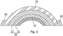
Fig. 2 is a schematic view showing Step 2 of the method for improving threshold voltage of the oxide semiconductor TFT provided by an embodiment of the present invention; -
Fig. 3 is a schematic view showing Step 2 of the method for improving threshold voltage of the oxide semiconductor TFT provided by another embodiment of the present invention; -
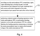
Fig. 4 is a schematic view showing a flowchart of the method for improving threshold voltage of the oxide semiconductor TFT provided by an embodiment of the present invention. - To further explain the technique means and effect of the present invention, the following uses preferred embodiments and drawings for detailed description.
- Referring to
Fig. 4 , the present invention provides a method for improving threshold voltage of oxide semiconductor TFT, comprising the steps of: - Step 1: as shown in
Fig. 1 , providing an oxide semiconductor thin film transistor (TFT), comprising: agate 10, agate insulating layer 20 covering thegate 10, anoxide semiconductor layer 30 disposed on thegate insulating layer 20, and asource 40 and adrain 50 disposed on theoxide semiconductor layer 30 spaced form each other with an interval. - Specifically, Step 1 further comprises: providing a flexible base, and the oxide semiconductor TFT being disposed on the flexible base.
- Preferably, the
oxide semiconductor layer 30 is made of indium gallium zinc oxide (IGZO). Thegate 10, thesource 40 and thedrain 50 are made of one or more of the materials of molybdenum (Mo), aluminum (Al), and titanium (Ti). Thegate insulating layer 20 comprise asilicon nitride layer 21 covering thegate 10, and asilicon oxide layer 22 coveringsilicon nitride layer 21. - Step 2: as shown in
Fig. 2 orFig. 3 , performing a default number of bending operations on the oxide semiconductor TFT, or performing a bending operation on the oxide semiconductor TFT for a default duration. The bending operation compressing or stretching theoxide semiconductor layer 30 to improve the threshold voltage of the oxide semiconductor TFT. - Preferably, in Step 2, the default number of bending operations is 100,000 times. Preferably, in Step 2, the default duration for the bending operation is longer than or equal to 45 days. Specifically, in Step 2, depending on actual needs, the bending operation can be opted to stretch the
oxide semiconductor layer 30 so that the threshold voltage of the oxide semiconductor TFT is reduced and gradually stabilized. Alternatively, the bending operation compresses theoxide semiconductor layer 30 so that the threshold voltage of the oxide semiconductor TFT is increased and gradually stabilized; for example, as shown inFig. 2 , in Step 2, by bending the oxide semiconductor TFT towards thegate 10 to stretch theoxide semiconductor layer 30, or, as shown inFig. 3 , in Step 2, by bending the oxide semiconductor TFT away from thegate 10 to compress theoxide semiconductor layer 30. - Specifically, in the first embodiment of the present invention, the oxide semiconductor TFT has a bending radius less than or equal to 3mm during the bending operation of 100,000 times. By bending the oxide semiconductor TFT to stretch the
oxide semiconductor layer 30 to improve the threshold voltage of the oxide semiconductor TFT, the relation between the threshold voltage of the oxide semiconductor TFT and the number of bending operations is shown in Table 1:Table 1: relation between the threshold voltage of the oxide semiconductor TFT and the number of bending operations with 3mm bending radius. Number of bending operations Threshold voltage 0 1.06V 10000 1.00V 30000 0.87V 60000 0.75V 100000 0.56V - As shown in Table 1, in the first embodiment of the present invention, the threshold voltage of the oxide semiconductor TFT decreases as the number of bending operations increases.
- Specifically, in the second embodiment of the present invention, the oxide semiconductor TFT has a bending radius less than or equal to 5mm during the bending operation of 100,000 times. By bending the oxide semiconductor TFT to stretch the
oxide semiconductor layer 30 to improve the threshold voltage of the oxide semiconductor TFT, the relation between the threshold voltage of the oxide semiconductor TFT and the number of bending operations is shown in Table 2:Table 2: relation between the threshold voltage of the oxide semiconductor TFT and the number of bending operations with 5mm bending radius. Number of bending operations Threshold voltage 0 1.06V 23000 1.11V 60000 1.01V 100000 1.04V - Comparing Table 1 and Table 2, when the bending radius is 3mm, the effect of bending on the threshold voltage of the oxide semiconductor TFT is more prominent than the bending radius of 5mm. As such, the bending operation is preferably to have a bending radius less than or equal to 3mm when bending the oxide semiconductor TFT.
- Specifically, in the third embodiment of the present invention, the oxide semiconductor TFT has a 3mm bending radius less for 45 days. By bending the oxide semiconductor TFT to stretch the
oxide semiconductor layer 30 to improve the threshold voltage of the oxide semiconductor TFT, the relation between the threshold voltage of the oxide semiconductor TFT and the number of days is shown in Table 3:Table 3: relation between the threshold voltage of the oxide semiconductor TFT and the number of days bending operations with 3mm bending radius. Number of days Threshold voltage 0 1.06V 15 -0.23V 22 -0.37V 30 -0.35V 45 -0.72V - As shown in Table 3, in the third embodiment of the present invention, the threshold voltage of the oxide semiconductor TFT decreases as the number of days increases.
- Specifically, in the fourth embodiment of the present invention, the oxide semiconductor TFT has a 5mm bending radius less for 45 days. By bending the oxide semiconductor TFT to stretch the
oxide semiconductor layer 30 to improve the threshold voltage of the oxide semiconductor TFT, the relation between the threshold voltage of the oxide semiconductor TFT and the number of days is shown in Table 4:Table 4: relation between the threshold voltage of the oxide semiconductor TFT and the number of days bending operations with 5mm bending radius. Number of days Threshold voltage 0 1.06V 15 0.19 V 22 0.04 V 30 0.09V 45 0.10V - Comparing Table 3 and Table 4, when the bending radius is 3mm, the effect of bending on the threshold voltage of the oxide semiconductor TFT is more prominent than the bending radius of 5mm. As such, the bending operation is preferably to have a bending radius less than or equal to 3mm when bending the oxide semiconductor TFT.
- It should be noted that the above embodiments perform bending to stretch the
oxide semiconductor layer 30. However, the present invention is not restricted to stretching. In other embodiments of the present invention, depending on needs, the present invention can also perform bending to compress theoxide semiconductor layer 30 to achieve improving the threshold of the oxide semiconductor TFT. - In summary, the present invention provides a method for improving threshold voltage of oxide semiconductor TFT, by bending the oxide semiconductor TFT for a default number of times or bending the oxide semiconductor TFT for a default duration, by bending the oxide semiconductor TFT to compress or stretch the oxide semiconductor layer to change the distance among the atoms in the channel of the oxide semiconductor TFT so as to change the energy difference between the inter-atom bonding orbital and anti-bonding orbital, resulting in controlling the threshold voltage of the oxide semiconductor TFT within a proper range to achieve improving the threshold voltage of the oxide semiconductor TFT.
- It should be noted that in the present disclosure the terms, such as, first, second are only for distinguishing an entity or operation from another entity or operation, and does not imply any specific relation or order between the entities or operations. Also, the terms "comprises", "include", and other similar variations, do not exclude the inclusion of other non-listed elements. Without further restrictions, the expression "comprises a..." does not exclude other identical elements from presence besides the listed elements.
- Embodiments of the present invention have been described, but not intending to impose any unduly constraint to the appended claims. Any modification of equivalent structure or equivalent process made according to the disclosure and drawings of the present invention, or any application thereof, directly or indirectly, to other related fields of technique, is considered encompassed in the scope of protection defined by the clams of the present invention.
wherein in Step 2, the default duration for the bending operation being longer than or equal to 45 days.
wherein the oxide semiconductor TFT having a bending radius less than or equal to 3mm during the bending operation.
wherein the gate, the source and the drain being made of one or more of the materials of molybdenum (Mo), aluminum (Al), and titanium (Ti).
wherein the gate insulating layer comprising a silicon nitride layer covering the gate, and a silicon oxide layer covering silicon nitride layer.
Claims (15)
- A method for improving threshold voltage of oxide semiconductor thin film transistor (TFT), comprising the steps of:Step 1: providing an oxide semiconductor TFT, comprising: a gate, a gate insulating layer covering the gate, an oxide semiconductor layer disposed on the gate insulating layer, and a source and a drain disposed on the oxide semiconductor layer spaced form each other with an interval;Step 2: performing a default number of bending operations on the oxide semiconductor TFT, or performing a bending operation on the oxide semiconductor TFT for a default duration; the bending operation compressing or stretching the oxide semiconductor layer to improve the threshold voltage of the oxide semiconductor TFT.
- The method for improving threshold voltage of oxide semiconductor TFT as claimed in Claim 1, wherein in Step 2, the default number of bending operations is more than or equal to 100,000 times.
- The method for improving threshold voltage of oxide semiconductor TFT as claimed in Claim 1, wherein in Step 2, the default duration for the bending operation is longer than or equal to 45 days.
- The method for improving threshold voltage of oxide semiconductor TFT as claimed in Claim 2, wherein the oxide semiconductor TFT has a bending radius less than or equal to 3mm during the bending operation.
- The method for improving threshold voltage of oxide semiconductor TFT as claimed in Claim 1, wherein in Step 2, the bending operation stretches the oxide semiconductor layer so that the threshold voltage of the oxide semiconductor TFT is reduced and gradually stabilized.
- The method for improving threshold voltage of oxide semiconductor TFT as claimed in Claim 1, wherein in Step 2, the bending operation compresses the oxide semiconductor layer so that the threshold voltage of the oxide semiconductor TFT is increased and gradually stabilized.
- The method for improving threshold voltage of oxide semiconductor TFT as claimed in Claim 1, wherein the oxide semiconductor layer is made of indium gallium zinc oxide (IGZO).
- The method for improving threshold voltage of oxide semiconductor TFT as claimed in Claim 1, wherein the gate, the source and the drain are made of one or more of the materials of molybdenum (Mo), aluminum (Al), and titanium (Ti).
- The method for improving threshold voltage of oxide semiconductor TFT as claimed in Claim 1, wherein the gate insulating layer comprise a silicon nitride layer covering the gate, and a silicon oxide layer covering silicon nitride layer.
- The method for improving threshold voltage of oxide semiconductor TFT as claimed in Claim 1, wherein Step 1 further comprises: providing a flexible base, and the oxide semiconductor TFT being disposed on the flexible base.
- A method for improving threshold voltage of oxide semiconductor thin film transistor (TFT), comprising the steps of:Step 1: providing an oxide semiconductor TFT, comprising: a gate, a gate insulating layer covering the gate, an oxide semiconductor layer disposed on the gate insulating layer, and a source and a drain disposed on the oxide semiconductor layer spaced form each other with an interval;Step 2: performing a default number of bending operations on the oxide semiconductor TFT, or performing a bending operation on the oxide semiconductor TFT for a default duration; the bending operation compressing or stretching the oxide semiconductor layer to improve the threshold voltage of the oxide semiconductor TFT;wherein in Step 2, the default number of bending operations being more than or equal to 100,000 times;
wherein in Step 2, the default duration for the bending operation being longer than or equal to 45 days;
wherein the oxide semiconductor TFT having a bending radius less than or equal to 3mm during the bending operation;
wherein the gate, the source and the drain being made of one or more of the materials of molybdenum (Mo), aluminum (Al), and titanium (Ti);
wherein the gate insulating layer comprising a silicon nitride layer covering the gate, and a silicon oxide layer covering silicon nitride layer. - The method for improving threshold voltage of oxide semiconductor TFT as claimed in Claim 11, wherein in Step 2, the bending operation stretches the oxide semiconductor layer so that the threshold voltage of the oxide semiconductor TFT is reduced and gradually stabilized.
- The method for improving threshold voltage of oxide semiconductor TFT as claimed in Claim 11, wherein in Step 2, the bending operation compresses the oxide semiconductor layer so that the threshold voltage of the oxide semiconductor TFT is increased and gradually stabilized.
- The method for improving threshold voltage of oxide semiconductor TFT as claimed in Claim 11, wherein the oxide semiconductor layer is made of indium gallium zinc oxide (IGZO).
- The method for improving threshold voltage of oxide semiconductor TFT as claimed in Claim 11, wherein Step 1 further comprises: providing a flexible base, and the oxide semiconductor TFT being disposed on the flexible base.
Applications Claiming Priority (2)
| Application Number | Priority Date | Filing Date | Title |
|---|---|---|---|
| CN201710477261.6A CN107403732B (en) | 2017-06-21 | 2017-06-21 | Method for Improving Threshold Voltage of Oxide Semiconductor Thin Film Transistor |
| PCT/CN2017/098105 WO2018232946A1 (en) | 2017-06-21 | 2017-08-18 | Method for improving threshold voltage of oxide semiconductor thin-film transistor |
Publications (3)
| Publication Number | Publication Date |
|---|---|
| EP3644347A1 true EP3644347A1 (en) | 2020-04-29 |
| EP3644347A4 EP3644347A4 (en) | 2021-03-10 |
| EP3644347B1 EP3644347B1 (en) | 2025-01-01 |
Family
ID=60405244
Family Applications (1)
| Application Number | Title | Priority Date | Filing Date |
|---|---|---|---|
| EP17915196.4A Active EP3644347B1 (en) | 2017-06-21 | 2017-08-18 | Method for improving threshold voltage of oxide semiconductor thin-film transistor |
Country Status (6)
| Country | Link |
|---|---|
| US (1) | US10204800B2 (en) |
| EP (1) | EP3644347B1 (en) |
| JP (1) | JP6972183B2 (en) |
| KR (1) | KR102265777B1 (en) |
| CN (1) | CN107403732B (en) |
| WO (1) | WO2018232946A1 (en) |
Family Cites Families (10)
| Publication number | Priority date | Publication date | Assignee | Title |
|---|---|---|---|---|
| JPH0448735A (en) * | 1990-06-15 | 1992-02-18 | Hitachi Ltd | Stabilizing method for characteristic of thin film transistor |
| JPH07176755A (en) * | 1993-12-21 | 1995-07-14 | Casio Comput Co Ltd | Method for correcting threshold voltage of thin film transistor |
| KR102436902B1 (en) * | 2010-04-02 | 2022-08-25 | 가부시키가이샤 한도오따이 에네루기 켄큐쇼 | Semiconductor device |
| US8841664B2 (en) * | 2011-03-04 | 2014-09-23 | Semiconductor Energy Laboratory Co., Ltd. | Semiconductor device |
| CN102983141B (en) * | 2011-09-02 | 2015-07-01 | 乐金显示有限公司 | Flat panel display device with oxide thin film transistors and method for fabricating the same |
| US8937307B2 (en) * | 2012-08-10 | 2015-01-20 | Semiconductor Energy Laboratory Co., Ltd. | Semiconductor device |
| KR102361966B1 (en) * | 2013-12-02 | 2022-02-14 | 가부시키가이샤 한도오따이 에네루기 켄큐쇼 | Display device and method for manufacturing the same |
| TWI517114B (en) * | 2014-09-26 | 2016-01-11 | 友達光電股份有限公司 | Display module having different curvature design |
| JP6357665B2 (en) * | 2014-12-05 | 2018-07-18 | 株式会社Joled | Thin film transistor substrate and manufacturing method thereof |
| CN106328693B (en) * | 2015-06-23 | 2019-07-05 | 群创光电股份有限公司 | Display panel |
-
2017
- 2017-06-21 CN CN201710477261.6A patent/CN107403732B/en active Active
- 2017-08-18 US US15/561,982 patent/US10204800B2/en active Active
- 2017-08-18 KR KR1020207001796A patent/KR102265777B1/en active Active
- 2017-08-18 JP JP2019570006A patent/JP6972183B2/en active Active
- 2017-08-18 WO PCT/CN2017/098105 patent/WO2018232946A1/en not_active Ceased
- 2017-08-18 EP EP17915196.4A patent/EP3644347B1/en active Active
Also Published As
| Publication number | Publication date |
|---|---|
| EP3644347B1 (en) | 2025-01-01 |
| KR20200018670A (en) | 2020-02-19 |
| JP2020524405A (en) | 2020-08-13 |
| CN107403732A (en) | 2017-11-28 |
| JP6972183B2 (en) | 2021-11-24 |
| KR102265777B1 (en) | 2021-06-16 |
| US10204800B2 (en) | 2019-02-12 |
| EP3644347A4 (en) | 2021-03-10 |
| WO2018232946A1 (en) | 2018-12-27 |
| US20180374713A1 (en) | 2018-12-27 |
| CN107403732B (en) | 2019-10-25 |
Similar Documents
| Publication | Publication Date | Title |
|---|---|---|
| CN104241298B (en) | TFT backplate structure and preparation method thereof | |
| CN104183608B (en) | TFT backplane structure and manufacturing method thereof | |
| CN105390551B (en) | Thin film transistor (TFT) and its manufacturing method, array substrate, display device | |
| CN106756877B (en) | C-axis crystalline IGZO thin film and preparation method thereof | |
| CN104037090B (en) | Oxide thin film transistor construction manufacturing method and oxide thin film transistor structure | |
| CN102800709B (en) | Driving device for thin film transistor | |
| CN106098560A (en) | The manufacture method of top gate type thin film transistor | |
| Chen et al. | Abnormal dual channel formation induced by hydrogen diffusion from SiN x interlayer dielectric in top gate a-InGaZnO transistors | |
| CN104241299B (en) | Oxide semiconductor TFT substrate manufacturing method and oxide semiconductor TFT substrate structure | |
| CN107579077A (en) | A kind of display panel, its preparation method and display device | |
| CN105514172B (en) | A kind of low-voltage transparent oxide film transistor and preparation method thereof | |
| US20140204305A1 (en) | Tft structure, lcd device, and method for manufacturing tft | |
| EP3644347B1 (en) | Method for improving threshold voltage of oxide semiconductor thin-film transistor | |
| CN106847828B (en) | Low-temperature polycrystalline silicon array substrate and manufacturing method thereof | |
| CN102290443B (en) | A kind of amorphous thin film transistor and preparation method thereof | |
| KR20120132130A (en) | thin film transistor and forming method of the same | |
| KR101273707B1 (en) | Thin film transistor and method for producing the same | |
| CN104157701B (en) | Manufacturing method and structure of oxide semiconductor TFT substrate | |
| US10224406B2 (en) | Array substrate including vertical TFT, and manufacturing method thereof | |
| CN109887991A (en) | A kind of lamination silicon doped stannum oxide thin film transistor (TFT) and preparation method thereof | |
| CN102779855A (en) | Double-schottky-junction zinc oxide semiconductor film transistor and manufacturing method | |
| CN202633321U (en) | Double-schottky junction zinc oxide semiconductor thin film transistor | |
| CN109888019B (en) | Heterostructure oxide thin film transistor based on quasi-modulation doping effect | |
| Zheng et al. | P‐1.39: High Performance Top Gage Oxide TFT Technology for Demux Driving Notebook LCD | |
| CN205335262U (en) | Resistance grid thin film transistor |
Legal Events
| Date | Code | Title | Description |
|---|---|---|---|
| STAA | Information on the status of an ep patent application or granted ep patent |
Free format text: STATUS: THE INTERNATIONAL PUBLICATION HAS BEEN MADE |
|
| PUAI | Public reference made under article 153(3) epc to a published international application that has entered the european phase |
Free format text: ORIGINAL CODE: 0009012 |
|
| STAA | Information on the status of an ep patent application or granted ep patent |
Free format text: STATUS: REQUEST FOR EXAMINATION WAS MADE |
|
| 17P | Request for examination filed |
Effective date: 20200110 |
|
| AK | Designated contracting states |
Kind code of ref document: A1 Designated state(s): AL AT BE BG CH CY CZ DE DK EE ES FI FR GB GR HR HU IE IS IT LI LT LU LV MC MK MT NL NO PL PT RO RS SE SI SK SM TR |
|
| AX | Request for extension of the european patent |
Extension state: BA ME |
|
| DAV | Request for validation of the european patent (deleted) | ||
| DAX | Request for extension of the european patent (deleted) | ||
| A4 | Supplementary search report drawn up and despatched |
Effective date: 20210205 |
|
| RIC1 | Information provided on ipc code assigned before grant |
Ipc: H01L 29/786 20060101ALI20210201BHEP Ipc: H01L 21/46 20060101AFI20210201BHEP Ipc: H01L 21/34 20060101ALI20210201BHEP |
|
| GRAP | Despatch of communication of intention to grant a patent |
Free format text: ORIGINAL CODE: EPIDOSNIGR1 |
|
| STAA | Information on the status of an ep patent application or granted ep patent |
Free format text: STATUS: GRANT OF PATENT IS INTENDED |
|
| INTG | Intention to grant announced |
Effective date: 20240930 |
|
| GRAS | Grant fee paid |
Free format text: ORIGINAL CODE: EPIDOSNIGR3 |
|
| GRAA | (expected) grant |
Free format text: ORIGINAL CODE: 0009210 |
|
| STAA | Information on the status of an ep patent application or granted ep patent |
Free format text: STATUS: THE PATENT HAS BEEN GRANTED |
|
| P01 | Opt-out of the competence of the unified patent court (upc) registered |
Free format text: CASE NUMBER: APP_59538/2024 Effective date: 20241103 |
|
| AK | Designated contracting states |
Kind code of ref document: B1 Designated state(s): AL AT BE BG CH CY CZ DE DK EE ES FI FR GB GR HR HU IE IS IT LI LT LU LV MC MK MT NL NO PL PT RO RS SE SI SK SM TR |
|
| REG | Reference to a national code |
Ref country code: GB Ref legal event code: FG4D |
|
| REG | Reference to a national code |
Ref country code: DE Ref legal event code: R096 Ref document number: 602017087162 Country of ref document: DE |
|
| REG | Reference to a national code |
Ref country code: CH Ref legal event code: EP |
|
| REG | Reference to a national code |
Ref country code: IE Ref legal event code: FG4D |
|
| REG | Reference to a national code |
Ref country code: LT Ref legal event code: MG9D |
|
| REG | Reference to a national code |
Ref country code: NL Ref legal event code: MP Effective date: 20250101 |
|
| REG | Reference to a national code |
Ref country code: AT Ref legal event code: MK05 Ref document number: 1757198 Country of ref document: AT Kind code of ref document: T Effective date: 20250101 |
|
| PG25 | Lapsed in a contracting state [announced via postgrant information from national office to epo] |
Ref country code: NL Free format text: LAPSE BECAUSE OF FAILURE TO SUBMIT A TRANSLATION OF THE DESCRIPTION OR TO PAY THE FEE WITHIN THE PRESCRIBED TIME-LIMIT Effective date: 20250101 |
|
| PG25 | Lapsed in a contracting state [announced via postgrant information from national office to epo] |
Ref country code: FI Free format text: LAPSE BECAUSE OF FAILURE TO SUBMIT A TRANSLATION OF THE DESCRIPTION OR TO PAY THE FEE WITHIN THE PRESCRIBED TIME-LIMIT Effective date: 20250101 |
|
| PG25 | Lapsed in a contracting state [announced via postgrant information from national office to epo] |
Ref country code: PL Free format text: LAPSE BECAUSE OF FAILURE TO SUBMIT A TRANSLATION OF THE DESCRIPTION OR TO PAY THE FEE WITHIN THE PRESCRIBED TIME-LIMIT Effective date: 20250101 |
|
| PG25 | Lapsed in a contracting state [announced via postgrant information from national office to epo] |
Ref country code: ES Free format text: LAPSE BECAUSE OF FAILURE TO SUBMIT A TRANSLATION OF THE DESCRIPTION OR TO PAY THE FEE WITHIN THE PRESCRIBED TIME-LIMIT Effective date: 20250101 |
|
| PG25 | Lapsed in a contracting state [announced via postgrant information from national office to epo] |
Ref country code: NO Free format text: LAPSE BECAUSE OF FAILURE TO SUBMIT A TRANSLATION OF THE DESCRIPTION OR TO PAY THE FEE WITHIN THE PRESCRIBED TIME-LIMIT Effective date: 20250401 Ref country code: IS Free format text: LAPSE BECAUSE OF FAILURE TO SUBMIT A TRANSLATION OF THE DESCRIPTION OR TO PAY THE FEE WITHIN THE PRESCRIBED TIME-LIMIT Effective date: 20250501 |
|
| PG25 | Lapsed in a contracting state [announced via postgrant information from national office to epo] |
Ref country code: HR Free format text: LAPSE BECAUSE OF FAILURE TO SUBMIT A TRANSLATION OF THE DESCRIPTION OR TO PAY THE FEE WITHIN THE PRESCRIBED TIME-LIMIT Effective date: 20250101 |
|
| PG25 | Lapsed in a contracting state [announced via postgrant information from national office to epo] |
Ref country code: LV Free format text: LAPSE BECAUSE OF FAILURE TO SUBMIT A TRANSLATION OF THE DESCRIPTION OR TO PAY THE FEE WITHIN THE PRESCRIBED TIME-LIMIT Effective date: 20250101 Ref country code: PT Free format text: LAPSE BECAUSE OF FAILURE TO SUBMIT A TRANSLATION OF THE DESCRIPTION OR TO PAY THE FEE WITHIN THE PRESCRIBED TIME-LIMIT Effective date: 20250502 |
|
| PG25 | Lapsed in a contracting state [announced via postgrant information from national office to epo] |
Ref country code: BG Free format text: LAPSE BECAUSE OF FAILURE TO SUBMIT A TRANSLATION OF THE DESCRIPTION OR TO PAY THE FEE WITHIN THE PRESCRIBED TIME-LIMIT Effective date: 20250101 Ref country code: GR Free format text: LAPSE BECAUSE OF FAILURE TO SUBMIT A TRANSLATION OF THE DESCRIPTION OR TO PAY THE FEE WITHIN THE PRESCRIBED TIME-LIMIT Effective date: 20250402 |
|
| PG25 | Lapsed in a contracting state [announced via postgrant information from national office to epo] |
Ref country code: AT Free format text: LAPSE BECAUSE OF FAILURE TO SUBMIT A TRANSLATION OF THE DESCRIPTION OR TO PAY THE FEE WITHIN THE PRESCRIBED TIME-LIMIT Effective date: 20250101 |
|
| PG25 | Lapsed in a contracting state [announced via postgrant information from national office to epo] |
Ref country code: CZ Free format text: LAPSE BECAUSE OF FAILURE TO SUBMIT A TRANSLATION OF THE DESCRIPTION OR TO PAY THE FEE WITHIN THE PRESCRIBED TIME-LIMIT Effective date: 20250101 |
|
| PG25 | Lapsed in a contracting state [announced via postgrant information from national office to epo] |
Ref country code: SE Free format text: LAPSE BECAUSE OF FAILURE TO SUBMIT A TRANSLATION OF THE DESCRIPTION OR TO PAY THE FEE WITHIN THE PRESCRIBED TIME-LIMIT Effective date: 20250101 |
|
| REG | Reference to a national code |
Ref country code: DE Ref legal event code: R097 Ref document number: 602017087162 Country of ref document: DE |
|
| PG25 | Lapsed in a contracting state [announced via postgrant information from national office to epo] |
Ref country code: SM Free format text: LAPSE BECAUSE OF FAILURE TO SUBMIT A TRANSLATION OF THE DESCRIPTION OR TO PAY THE FEE WITHIN THE PRESCRIBED TIME-LIMIT Effective date: 20250101 |
|
| PG25 | Lapsed in a contracting state [announced via postgrant information from national office to epo] |
Ref country code: DK Free format text: LAPSE BECAUSE OF FAILURE TO SUBMIT A TRANSLATION OF THE DESCRIPTION OR TO PAY THE FEE WITHIN THE PRESCRIBED TIME-LIMIT Effective date: 20250101 |
|
| PGFP | Annual fee paid to national office [announced via postgrant information from national office to epo] |
Ref country code: DE Payment date: 20250820 Year of fee payment: 9 |
|
| PG25 | Lapsed in a contracting state [announced via postgrant information from national office to epo] |
Ref country code: IT Free format text: LAPSE BECAUSE OF FAILURE TO SUBMIT A TRANSLATION OF THE DESCRIPTION OR TO PAY THE FEE WITHIN THE PRESCRIBED TIME-LIMIT Effective date: 20250101 |
|
| PG25 | Lapsed in a contracting state [announced via postgrant information from national office to epo] |
Ref country code: EE Free format text: LAPSE BECAUSE OF FAILURE TO SUBMIT A TRANSLATION OF THE DESCRIPTION OR TO PAY THE FEE WITHIN THE PRESCRIBED TIME-LIMIT Effective date: 20250101 |
|
| PG25 | Lapsed in a contracting state [announced via postgrant information from national office to epo] |
Ref country code: RO Free format text: LAPSE BECAUSE OF FAILURE TO SUBMIT A TRANSLATION OF THE DESCRIPTION OR TO PAY THE FEE WITHIN THE PRESCRIBED TIME-LIMIT Effective date: 20250101 |
|
| PG25 | Lapsed in a contracting state [announced via postgrant information from national office to epo] |
Ref country code: SK Free format text: LAPSE BECAUSE OF FAILURE TO SUBMIT A TRANSLATION OF THE DESCRIPTION OR TO PAY THE FEE WITHIN THE PRESCRIBED TIME-LIMIT Effective date: 20250101 |
|
| PLBE | No opposition filed within time limit |
Free format text: ORIGINAL CODE: 0009261 |
|
| STAA | Information on the status of an ep patent application or granted ep patent |
Free format text: STATUS: NO OPPOSITION FILED WITHIN TIME LIMIT |
|
| REG | Reference to a national code |
Ref country code: CH Ref legal event code: L10 Free format text: ST27 STATUS EVENT CODE: U-0-0-L10-L00 (AS PROVIDED BY THE NATIONAL OFFICE) Effective date: 20251112 |
|
| REG | Reference to a national code |
Ref country code: DE Ref legal event code: R079 Ref document number: 602017087162 Country of ref document: DE Free format text: PREVIOUS MAIN CLASS: H01L0021460000 Ipc: H10P0095000000 |
|
| 26N | No opposition filed |
Effective date: 20251002 |
|
| REG | Reference to a national code |
Ref country code: CH Ref legal event code: H13 Free format text: ST27 STATUS EVENT CODE: U-0-0-H10-H13 (AS PROVIDED BY THE NATIONAL OFFICE) Effective date: 20260324 |
|
| PG25 | Lapsed in a contracting state [announced via postgrant information from national office to epo] |
Ref country code: MC Free format text: LAPSE BECAUSE OF FAILURE TO SUBMIT A TRANSLATION OF THE DESCRIPTION OR TO PAY THE FEE WITHIN THE PRESCRIBED TIME-LIMIT Effective date: 20250101 |
|
| PG25 | Lapsed in a contracting state [announced via postgrant information from national office to epo] |
Ref country code: LU Free format text: LAPSE BECAUSE OF NON-PAYMENT OF DUE FEES Effective date: 20250818 |
|
| PG25 | Lapsed in a contracting state [announced via postgrant information from national office to epo] |
Ref country code: CH Free format text: LAPSE BECAUSE OF NON-PAYMENT OF DUE FEES Effective date: 20250831 |
|
| GBPC | Gb: european patent ceased through non-payment of renewal fee |
Effective date: 20250818 |