EP3643960A1 - Wavelength conversion module, method of forming the same and projection apparatus - Google Patents
Wavelength conversion module, method of forming the same and projection apparatus Download PDFInfo
- Publication number
- EP3643960A1 EP3643960A1 EP19203822.2A EP19203822A EP3643960A1 EP 3643960 A1 EP3643960 A1 EP 3643960A1 EP 19203822 A EP19203822 A EP 19203822A EP 3643960 A1 EP3643960 A1 EP 3643960A1
- Authority
- EP
- European Patent Office
- Prior art keywords
- wavelength conversion
- region
- conversion module
- substrate
- diffuse reflection
- Prior art date
- Legal status (The legal status is an assumption and is not a legal conclusion. Google has not performed a legal analysis and makes no representation as to the accuracy of the status listed.)
- Granted
Links
Images





Classifications
-
- G—PHYSICS
- G02—OPTICS
- G02B—OPTICAL ELEMENTS, SYSTEMS OR APPARATUS
- G02B26/00—Optical devices or arrangements for the control of light using movable or deformable optical elements
- G02B26/007—Optical devices or arrangements for the control of light using movable or deformable optical elements the movable or deformable optical element controlling the colour, i.e. a spectral characteristic, of the light
- G02B26/008—Optical devices or arrangements for the control of light using movable or deformable optical elements the movable or deformable optical element controlling the colour, i.e. a spectral characteristic, of the light in the form of devices for effecting sequential colour changes, e.g. colour wheels
-
- H—ELECTRICITY
- H10—SEMICONDUCTOR DEVICES; ELECTRIC SOLID-STATE DEVICES NOT OTHERWISE PROVIDED FOR
- H10H—INORGANIC LIGHT-EMITTING SEMICONDUCTOR DEVICES HAVING POTENTIAL BARRIERS
- H10H20/00—Individual inorganic light-emitting semiconductor devices having potential barriers, e.g. light-emitting diodes [LED]
- H10H20/80—Constructional details
- H10H20/85—Packages
- H10H20/851—Wavelength conversion means
- H10H20/8515—Wavelength conversion means not being in contact with the bodies
-
- H—ELECTRICITY
- H10—SEMICONDUCTOR DEVICES; ELECTRIC SOLID-STATE DEVICES NOT OTHERWISE PROVIDED FOR
- H10H—INORGANIC LIGHT-EMITTING SEMICONDUCTOR DEVICES HAVING POTENTIAL BARRIERS
- H10H20/00—Individual inorganic light-emitting semiconductor devices having potential barriers, e.g. light-emitting diodes [LED]
- H10H20/80—Constructional details
- H10H20/85—Packages
- H10H20/851—Wavelength conversion means
- H10H20/8511—Wavelength conversion means characterised by their material, e.g. binder
- H10H20/8512—Wavelength conversion materials
-
- F—MECHANICAL ENGINEERING; LIGHTING; HEATING; WEAPONS; BLASTING
- F21—LIGHTING
- F21K—NON-ELECTRIC LIGHT SOURCES USING LUMINESCENCE; LIGHT SOURCES USING ELECTROCHEMILUMINESCENCE; LIGHT SOURCES USING CHARGES OF COMBUSTIBLE MATERIAL; LIGHT SOURCES USING SEMICONDUCTOR DEVICES AS LIGHT-GENERATING ELEMENTS; LIGHT SOURCES NOT OTHERWISE PROVIDED FOR
- F21K9/00—Light sources using semiconductor devices as light-generating elements, e.g. using light-emitting diodes [LED] or lasers
- F21K9/60—Optical arrangements integrated in the light source, e.g. for improving the colour rendering index or the light extraction
- F21K9/64—Optical arrangements integrated in the light source, e.g. for improving the colour rendering index or the light extraction using wavelength conversion means distinct or spaced from the light-generating element, e.g. a remote phosphor layer
-
- G—PHYSICS
- G02—OPTICS
- G02B—OPTICAL ELEMENTS, SYSTEMS OR APPARATUS
- G02B26/00—Optical devices or arrangements for the control of light using movable or deformable optical elements
-
- G—PHYSICS
- G03—PHOTOGRAPHY; CINEMATOGRAPHY; ANALOGOUS TECHNIQUES USING WAVES OTHER THAN OPTICAL WAVES; ELECTROGRAPHY; HOLOGRAPHY
- G03B—APPARATUS OR ARRANGEMENTS FOR TAKING PHOTOGRAPHS OR FOR PROJECTING OR VIEWING THEM; APPARATUS OR ARRANGEMENTS EMPLOYING ANALOGOUS TECHNIQUES USING WAVES OTHER THAN OPTICAL WAVES; ACCESSORIES THEREFOR
- G03B21/00—Projectors or projection-type viewers; Accessories therefor
- G03B21/14—Details
- G03B21/20—Lamp housings
-
- G—PHYSICS
- G03—PHOTOGRAPHY; CINEMATOGRAPHY; ANALOGOUS TECHNIQUES USING WAVES OTHER THAN OPTICAL WAVES; ELECTROGRAPHY; HOLOGRAPHY
- G03B—APPARATUS OR ARRANGEMENTS FOR TAKING PHOTOGRAPHS OR FOR PROJECTING OR VIEWING THEM; APPARATUS OR ARRANGEMENTS EMPLOYING ANALOGOUS TECHNIQUES USING WAVES OTHER THAN OPTICAL WAVES; ACCESSORIES THEREFOR
- G03B21/00—Projectors or projection-type viewers; Accessories therefor
- G03B21/14—Details
- G03B21/20—Lamp housings
- G03B21/2006—Lamp housings characterised by the light source
- G03B21/2033—LED or laser light sources
- G03B21/204—LED or laser light sources using secondary light emission, e.g. luminescence or fluorescence
-
- H—ELECTRICITY
- H10—SEMICONDUCTOR DEVICES; ELECTRIC SOLID-STATE DEVICES NOT OTHERWISE PROVIDED FOR
- H10H—INORGANIC LIGHT-EMITTING SEMICONDUCTOR DEVICES HAVING POTENTIAL BARRIERS
- H10H20/00—Individual inorganic light-emitting semiconductor devices having potential barriers, e.g. light-emitting diodes [LED]
- H10H20/80—Constructional details
- H10H20/85—Packages
- H10H20/851—Wavelength conversion means
- H10H20/8514—Wavelength conversion means characterised by their shape, e.g. plate or foil
-
- H—ELECTRICITY
- H10—SEMICONDUCTOR DEVICES; ELECTRIC SOLID-STATE DEVICES NOT OTHERWISE PROVIDED FOR
- H10H—INORGANIC LIGHT-EMITTING SEMICONDUCTOR DEVICES HAVING POTENTIAL BARRIERS
- H10H20/00—Individual inorganic light-emitting semiconductor devices having potential barriers, e.g. light-emitting diodes [LED]
- H10H20/80—Constructional details
- H10H20/85—Packages
- H10H20/851—Wavelength conversion means
- H10H20/8516—Wavelength conversion means having a non-uniform spatial arrangement or non-uniform concentration, e.g. patterned wavelength conversion layer or wavelength conversion layer with a concentration gradient
-
- H—ELECTRICITY
- H10—SEMICONDUCTOR DEVICES; ELECTRIC SOLID-STATE DEVICES NOT OTHERWISE PROVIDED FOR
- H10H—INORGANIC LIGHT-EMITTING SEMICONDUCTOR DEVICES HAVING POTENTIAL BARRIERS
- H10H20/00—Individual inorganic light-emitting semiconductor devices having potential barriers, e.g. light-emitting diodes [LED]
- H10H20/01—Manufacture or treatment
- H10H20/036—Manufacture or treatment of packages
- H10H20/0361—Manufacture or treatment of packages of wavelength conversion means
Definitions
- the invention relates to an optical module, a method of forming the same and an optical apparatus including the optical module. More particularly, the invention relates to a wavelength conversion module, a method of forming the same and a projection apparatus including the wavelength conversion module.
- laser diodes may have a luminous efficiency of about 20% higher than light-emitting diodes
- the technique of using laser light sources to excite phosphor for producing pure color light beams has been developed, so that the limitation in luminous efficiency of the light-emitting diodes may be broken.
- the conventional manufacture method for a reflective layer on a phosphor wheel may generally involve vacuum plating or mixed glue coating.
- the luminous efficiency, thermal conductivity coefficient, or reliability of the phosphor wheel may be subjected to be compromised due to limitations in manufacturing cost, material selection, thickness of the phosphor wheel.
- the invention provides a wavelength conversion module and a projection apparatus which may be used to provide preferable conversion efficiency, reliability or optical quality.
- the invention provides a method of forming a wavelength conversion module, and the wavelength conversion module as such formed may have preferable conversion efficiency and reliability.
- an embodiment of the invention provides a wavelength conversion module.
- the wavelength conversion module includes a substrate and a wavelength conversion layer.
- the substrate has a rough surface including two first regions and a second region, and the second region is located between the two first regions in a radial direction on the substrate.
- the wavelength conversion layer is located on the substrate and includes a wavelength conversion material, a bonding material and a plurality of diffuse reflection particles.
- the wavelength conversion material is distributed in the bonding material.
- the diffuse reflection particles are located on the rough surface of the substrate and located between the wavelength conversion material and the substrate. A second density of the diffuse reflection particles in the second region is greater than a first density of the diffuse reflection particles in one of the two first regions.
- the second density or the first density of the plurality of diffuse reflection particles may refer to a concentration percentage by volume of the plurality of diffuse reflection particles.
- a second concentration percentage by volume of the plurality of diffuse reflection particles in the second region may range from 60% to 100%.
- a second surface roughness of the second region may be greater than a first surface roughness of one of the two first regions.
- a second surface roughness of the second region may be less than or equal to a first surface roughness of one of the two first regions.
- a second surface roughness of the second region may range from 10 ⁇ m to 100 ⁇ m.
- second particle gaps between the plurality of diffuse reflection particles in the second region may be smaller than second particle gaps between the plurality of diffuse reflection particles in one of the two first regions.
- the rough surface of the substrate may comprise a plurality of concave-convex structures.
- a second average depth of the plurality of concave-convex structures distributed in the second region may be greater than or equal to a first average depth of the plurality of concave-convex structures distributed in one of the two first regions.
- the wavelength conversion module may further comprise an oxide ceramic layer, located on the rough surface of the substrate.
- the oxide ceramic layer and the plurality of diffuse reflection particles may jointly form a reflective layer.
- the reflective layer may comprises two first reflective regions, respectively located across the two first regions; and a second reflective region, located across the second region, wherein a first thickness of one of the two first reflective regions is less than a second thickness of the second reflective region.
- the first thickness of one of the two first reflective regions may be less than 0.05 mm, and/or the second thickness of the second reflective region may range from 0.02 mm to 0.15 mm.
- a material of the oxide ceramic layer may comprise aluminum oxide or titanium oxide.
- an embodiment of the invention provides a projection apparatus.
- the projection apparatus includes an abovementioned wavelength conversion module, an excitation light source, a light valve and a projection lens.
- the excitation light source is configured to emit an excitation light beam, and the excitation light beam may be transmitted to the wavelength conversion module and converted into an illumination beam by the wavelength conversion module.
- the light valve is located on a transmittance path of the illumination beam and configured to convert the illumination beam to an image beam.
- the projection lens is located on a transmission path of the image beam and configured to project the image beam.
- the projection apparatus may further comprise a substrate, having a rough surface comprising two first regions and a second region, wherein the second region is located between the two first regions in a radial direction on the substrate; and a wavelength conversion layer, located on the substrate and comprising a wavelength conversion material, a bonding material and a plurality of diffuse reflection particles, wherein the wavelength conversion material is distributed in the bonding material, and the plurality of diffuse reflection particles are located on the rough surface of the substrate, and the plurality of diffuse reflection particles are located between the wavelength conversion material and the substrate, and wherein a second concentration percentage by volume of the plurality of diffuse reflection particles in the second region is greater than or equal to a first concentration percentage by volume of the plurality of diffuse reflection particles in one of the two first regions; and an excitation light source, configured to emit an excitation light beam, wherein the excitation light beam is transmitted to the wavelength conversion module and converted into an illumination beam by the wavelength conversion module; a light valve, located on a transmission path of the illumination beam and configured to convert the illumination beam into
- the excitation light beam when the excitation light beam is transmitted to the wavelength conversion module, the excitation light beam may form a spot on the wavelength conversion module, and a second energy density of a part of the spot irradiated on the second region may be greater than a first energy density of another part of the spot irradiated on one of the two first regions.
- the second concentration percentage by volume of the plurality of diffuse reflection particles in the second region may range from 60% to 100%.
- a second surface roughness of the second region may be greater than a first surface roughness of one of the two first regions.
- a second surface roughness of the second region may be less than or equal to a first surface roughness of one of the two first regions.
- a second surface roughness of the second region may range from 10 ⁇ m to 100 ⁇ m.
- second particle gaps between the plurality of diffuse reflection particles in the second region may be smaller than first particle gaps between the plurality of diffuse reflection particles in one of the two first regions.
- the projection apparatus may further comprise an oxide ceramic layer, located on the rough surface of the substrate.
- a material of the oxide ceramic layer may comprise aluminum oxide or titanium oxide.
- an embodiment of the invention provides a method of forming a wavelength conversion module.
- the method includes the following steps.
- a rough surface is formed on a substrate.
- the rough surface includes two first regions and a second region, and the second region is located between the two first regions in a radial direction on the substrate.
- a plurality of diffuse reflection particles is coated on the rough surface of the substrate, and a second concentration percentage by volume of the diffuse reflection particles in the second region is greater than or equal to a first concentration percentage by volume of the diffuse reflection particles in one of two the first regions.
- a wavelength conversion material and a bonding material are coated on the substrate to form a wavelength conversion layer, and the diffuse reflection particles are located between the wavelength conversion material and the substrate.
- a method of forming the rough surface on the substrate may comprise a chemical etching, a sandblasting, a grinding or a plasma electrolytic oxidation process.
- a method of coating the plurality of diffuse reflection particles on the rough surface of the substrate comprises a dispensing, a spray-on or a printing process.
- the embodiments of the invention achieve at least one of the following advantages or effects.
- various distribution densities of the diffuse reflection particles in different regions on the substrate may be achieved by disposing a rough surface on the substrate of the wavelength conversion module. Due to such-distributed diffuse reflection particles which are used for forming a wavelength conversion layer, a preferable combination of reflectivity, heat resistance, reliability, and manufacture cost of the wavelength conversion layer may be thus achieved.
- the wavelength conversion layer of the wavelength conversion module may have a preferable conversion efficiency and a preferable attachment with the substrate. As such, the reliability of the wavelength conversion module may be improved.
- main part of the laser spot may be directed at an area with more diffuse reflection particles and less bonding material.
- the risk of degradation and/or burnout caused from the bonding material which may be less heat-resistive may be avoided. Therefore, a preferable optical quality and reliability may be arrived at.
- various densities of the diffuse reflection particles used for the wavelength conversion layer in different areas of the substrate may be controlled by forming a rough surface on the substrate, such that the wavelength conversion module can have a preferable reliability and conversion efficiency.
- One of the two manufacturing methods involves a vacuum plating where a silver film, an aluminum film, a dielectric medium film or a mixed stack thereof may be plated on a heat dissipation substrate.
- the other involves processes such as printing, spray-on and dispensing onto a heat dissipation substrate a mixture of diffuse reflection particles with organic or inorganic glue, so as to form a reflective layer.
- requirements in reflectivity, thermal conductivity and reliability may be achieved with the consideration of the thickness of the reflective layer, the concentration of the diffuse reflection particles and the amount of the glue, which may a low thermal conductivity coefficient, used in the mixture.
- FIG. 1 is a schematic structure view of a projection apparatus according to an embodiment of the invention.
- FIG. 2A is a schematic top-view of a wavelength conversion module depicted in FIG. 1 .
- FIG. 2B is a schematic cross-sectional view of the wavelength conversion module depicted in FIG. 2A .
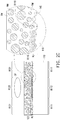
- FIG. 2C is a partially enlarged view of the wavelength conversion module depicted in FIG. 2B .
- a projection apparatus 200 includes an excitation light source 210, a dichroic unit 220, a wavelength conversion module 100, a light valve 250 and a projection lens 260.
- the light valve 250 is, for example, a digital micro-mirror device (DMD) or a liquid-crystal-on-silicon panel (LCOS panel).
- DMD digital micro-mirror device
- LCOS panel liquid-crystal-on-silicon panel
- the light valve 250 may be a transmissive liquid crystal panel or other light beam modulators.
- the excitation light source 210 is configured to emit an excitation light beam 50.
- the excitation light source 210 is a laser source
- the excitation light beam 50 is a blue laser beam.
- the excitation light source 210 may include a plurality of blue laser diodes (not shown) arranged in an array, but the invention is not limited thereto.
- the dichroic unit 220 is disposed on a transmission path of the excitation light beam 50 and located between the excitation light source 210 and the wavelength conversion module 100.
- the dichroic unit 220 may be a dichroic mirror, a partially transmissive and partially reflective component, a polarizing dichroic mirror or other various components capable of dichotomizing the light beam.
- the dichroic unit 220 may, for example, allow a light beam with a blue wavelength to penetrate and reflect light beams with other color wavelengths (e.g., red, green, yellow and so on).
- the dichroic unit 220 may allow the excitation light beam 50 with a blue wavelength to penetrate, and in this way, the excitation light beam 50 may penetrate the dichroic unit 220 to be incident onto the wavelength conversion module 100.
- the wavelength conversion module 100 is located on the transmission path of the excitation light beam 50.
- the wavelength conversion module 100 includes at least one wavelength conversion region WR and an optical region (which is illustrated as TR in FIG. 2A ) which may allow a light beam irradiating thereon to penetrate.
- the optical region TR may reflect the excitation light beam. For instance, referring to FIG. 1 to FIG.
- the at least one wavelength conversion region WR of the wavelength conversion module 100 is configured to convert the excitation light beam 50 into at least one wavelength conversion beam 60, and the light transmissive region TR of the wavelength conversion module 100 is configured to allow the excitation light beam 50 to pass through so that it may be transmitted to a subsequent optical component.
- the wavelength conversion module 100 includes a substrate 110 and a wavelength conversion layer 120.
- the substrate 110 has an axial center O located at the center of the substrate 110.
- the wavelength conversion layer 120 is located on the substrate 110, is disposed corresponding to the at least one wavelength conversion region WR and includes a wavelength conversion material WM, a bonding material BM and a plurality of diffuse reflection particles RM.
- a material of the substrate 110 may be aluminum, and the diffuse reflection particles RM may be white scattering particles such as titanium dioxide (TiO 2 ), silicon dioxide (SiO 2 ), aluminum oxide (Al 2 O 3 ), boron nitride (BN) or zirconium dioxide (ZrO 2 ), but the invention is not limited thereto.
- the bonding material BM may be, for example, organic glue or inorganic glue, such as silica gel.
- the substrate 110 has a rough surface R110.
- the rough surface R110 includes two first regions R111 and a second region R112.
- the second region R112 is located between the two first regions R111 in a radial direction R on the substrate 110.
- the wavelength conversion material WM is distributed in the bonding material BM, and the wavelength conversion material WM, for example, may be used to absorb the blue laser beam and emit a conversion beam with a different color wavelength from that of the blue laser beam.
- the wavelength conversion material may be phosphor particles which are excited to emit a color light.
- the diffuse reflection particles RM are located on the rough surface R110 of the substrate 110 and located between the wavelength conversion material WM and the substrate 110.
- a second density of the diffuse reflection particles RM in the second region R112 is greater than a first density of the diffuse reflection particles RM in one of the first regions R111.
- the second or first density of the diffuse reflection particles RM refers to a concentration percentage by volume of the diffuse reflection particles RM, and a second concentration percentage by volume of the diffuse reflection particles in the second region R112 ranges from 60% to 100%.
- second particle gaps between the diffuse reflection particles RM in the second region R112 are smaller than first particle gaps between the diffuse reflection particles RM in one of the two first regions R111.
- the excitation light beam 50 may be more subjected to be reflected, such that the wavelength conversion module 100 may have a preferable reflectivity.
- the bonding material BM in the second region R112 may be less, such that risks of degradation and/or burnout caused from the poor high-temperature resistance of the bonding material BM may be avoided.
- the wavelength conversion layer 120 located within the second region R112 is capable of bearing a greater laser energy.
- a second surface roughness (Ra) of the second region R112 of the rough surface R110 may be greater than a first surface roughness of one of the two first regions R111.
- a second maximum height of profile (Ry) of the second region R112 may be greater than a first maximum height of profile of one of the two first regions R111.
- the second surface roughness (Ra) of the second region R112 of the rough surface R110 ranges from 10 ⁇ m to 100 ⁇ m.
- the maximum height of profile (Ry) of the second region R112 is approximately less than 0.1 mm. It should be noted that the values mentioned are used only for examples and are not intended to limit the invention.
- the second surface roughness (Ra) of the second region R112 of the rough surface R110 may be less than or equal to the first surface roughness of one of the two first regions R111, and the first surface roughness of one of the two first regions R111 may be the same or different, but the invention is not limited thereto.
- Two first regions R111 may be smoother.
- at least one of the first regions R111 may be a rough surface, such that in the embodiment, a preferable bonding force may be provided between the wavelength conversion material WM and the bonding material BM coated in the two first regions R111 of the heat dissipation substrate 110, so as to improve the reliability of the wavelength conversion module 100.
- the invention is not limited thereto.
- the wavelength conversion module 100 further includes an oxide ceramic layer 140 located on the rough surface R110 of the substrate 110.
- a material of the oxide ceramic layer 140 may include aluminum oxide or titanium oxide, which may diffusively reflect the light.
- the oxide ceramic layer 140 and the diffuse reflection particles RM jointly form a reflective layer RL, and the reflective layer RL includes two first reflective regions R121 and a second reflective region R122.
- the two first reflective regions R121 are respectively located across the two first regions Rill.
- the second reflective region R122 is located across the second region R112, and a first thickness of one of the first reflective regions R121 is less than a second thickness of the second reflective region R122.
- the first thickness of one of the first reflective regions R121 is less than 0.05 mm
- the second thickness of the second reflective region R122 ranges from 0.02 mm to 0.15 mm. It should be noted that the values mentioned are used only for examples and are not intended to limit the invention.
- the excitation light beam 50 when the excitation light beam 50 is transmitted to the wavelength conversion module 100, the excitation light beam 50 may form a spot SP on the wavelength conversion module 100, and when the excitation light beam 50 irradiates onto the wavelength conversion module 100, the excitation light beam 50 is reflected by the reflective layer RL, such that the wavelength conversion module 100 may have a preferable reflectivity. Additionally, referring to FIG. 1 and FIG. 2C , in the embodiment, when the excitation light beam 50 is transmitted to the wavelength conversion module 100, the excitation light beam 50 may form a spot SP on the wavelength conversion module 100, and when the excitation light beam 50 irradiates onto the wavelength conversion module 100, the excitation light beam 50 is reflected by the reflective layer RL, such that the wavelength conversion module 100 may have a preferable reflectivity. Additionally, referring to FIG.
- locations of the first regions R111 and the second region 112 on the wavelength conversion module 100 and the ratios of their widths may be configured based on the energy distribution of the spot SP, such that the energy density of the part of the spot SP irradiating on the second region R112 is greater than the energy density of another part of the spot SP irradiating on one of the first regions R111.
- the laser spot SP mostly on a region which includes more diffuse reflection particles and less bonding material BM, the risk of degradation and/or burnout caused from the bonding material which may be less heat-resistive may be avoided, so as to achieve a preferable optical quality and reliability.
- the reflectivity, heat resistance, reliability and cost of the wavelength conversion layer 120 may be maintained. Meanwhile, with different surface roughness configured for different regions of the rough surface R110 of the substrate 110 of the wavelength conversion module 100, the wavelength conversion layer 120 of the wavelength conversion module 100 may have a preferable attachment to the substrate 110. As such, the reflectivity, thermal conductivity and the conversion efficiency of the wavelength conversion module 100 may be improved, while maintaining a preferable reliability and low cost.
- the optical region (which is illustrated as TR in FIG. 2A ) of the wavelength conversion module 100 may include a hollow region (which is not illustrated) and a diffuser 130 disposed corresponding to the hollow region.
- the diffuser 130 is configured to diffuse the excitation light beam to form a diffused light beam, thereby mitigating laser speckles caused from the excitation light beam 50.
- the wavelength conversion module 100 is a transmissive wavelength conversion module 100
- the optical region (which is illustrated as TR in FIG. 2A ) is configured to allow the excitation light beam 50 to penetrate.
- the optical region may be a light reflective region.
- the wavelength conversion module 100 further includes a first driving device MR configured to drive the optical region (which is illustrated as TR in FIG. 2A ) and the at least one wavelength conversion region WR to enter an irradiation range of the excitation light beam 50 at different times, such that the excitation light beam 50 may, for example, selectively pass through or may be converted into the wavelength conversion beam 60.
- a first driving device MR configured to drive the optical region (which is illustrated as TR in FIG. 2A ) and the at least one wavelength conversion region WR to enter an irradiation range of the excitation light beam 50 at different times, such that the excitation light beam 50 may, for example, selectively pass through or may be converted into the wavelength conversion beam 60.
- the excitation light beam 50 may penetrate the wavelength conversion module 100 and be transmitted to a light filter module 230 by a light transmission module LT, but the invention is not limited thereto.
- the excitation light beam 50 is converted into the at least one wavelength conversion beam 60 by the at least one wavelength conversion region WR.
- at least one wavelength conversion beam 60 from the wavelength conversion module 100 may be guided to the dichroic unit 220 and reflected towards the subsequent light filter module 230.
- the projection apparatus 200 further includes the light filter module 230 described above.
- the light filter module 230 is located on the transmission paths of the excitation light beam 50 and the wavelength conversion beam 60 and includes a light filter region (not shown) and a light transparent region (not shown).
- the light filter module 230 further includes a second driving device (not shown) configured to drive the light filter region (not shown) to enter an irradiation range of the wavelength conversion beam 60 at different times, thereby forming a red color light beam and a red color light beam and a green color light beam.
- the light transparent region may also enter the irradiation range of the excitation light beam 50 which is transmitted to the light filter module 230 at different times, thereby forming a blue color light beam.
- the excitation light beam 50 and the wavelength conversion beam 60 are time-sequentially converted into an illumination beam 70 having various color wavelengths.
- the projection apparatus 200 further includes a light-homogenizing component 240 located on a transmission path of the illumination beam 70.
- the light-homogenizing component 240 includes an integrator, but the invention is not limited thereto.
- the light-homogenizing component 240 may homogenize the illumination beam 70 and transmit it to the light valve 250.
- the light valve 250 is located on the transmittance path of the illumination beam 70 and configured to convert the illumination beam 70 into an image beam 80.
- the projection lens 260 is located on a transmission path of the image beam 80 and configured to project the image beam 80, thereby projecting the image beam 80 onto a screen (not shown) to form an image.
- the light valve 250 sequentially converts the illumination beam 70 into an image beam 80 having different color wavelengths and then the image beam 80 is transmitted to the projection lens 260. Therefore, a colorful image may be formed by the image beam 80 from the light valve 250.
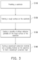
- FIG. 3 is a method of forming a wavelength conversion module according to an embodiment of the invention.
- FIG. 4A to FIG. 4D are schematic views illustrating a manufacturing process of a wavelength conversion module according to an embodiment of the invention.
- a substrate 110' is provided in step S110.
- a rough surface R110 is formed on the substrate 110'.
- the step 120 of forming the rough surface R110 on the substrate 110' includes a chemical etching, a sandblasting, a grinding or a plasma electrolytic oxidation (PEO) process.
- PEO plasma electrolytic oxidation
- the substrate 110 may be placed in a plating solution, and a high-voltage arc may be caused above the surface of the substrate 110 to change the surface structure, so as to form the rough surface R110. Additionally, the rough surface R110 formed by this process may have an oxide ceramic layer 140 thereon. In this way, a substrate 110 as illustrated in FIG. 4B may be formed.
- step S130 a plurality of diffuse reflection particles RM are coated on the rough surface R110 of the substrate 110.
- the second concentration percentage by volume of the diffuse reflection particles RM in a second region R112 is greater than or equal to the first concentration percentage by volume of the diffuse reflection particles RM in each first region R111.
- of the step of coating the diffuse reflection particles RM on the rough surface R110 of the substrate 110 includes: mixing the diffuse reflection particles RM into alcohol or other dispersing solvents; and then coating the mixture onto the rough surface R110 of the substrate 110 by a dispensing, spray-on or a printing process.
- a screen used during the printing process may be so designed that an area corresponding to the second region R112 of the rough surface R112 may have greater pores and that another area corresponding to the two first regions R111 of the rough surface R110 may have smaller pores, such that a second density of the diffuse reflection particles RM in the second region R112 is greater than a first density of the diffuse reflection particles RM in one of the first regions R111.
- a dispensing route may be so designed that an area corresponding to the second region R112 of the rough surface R110 may be dispensed with a slow coating speed and that another area corresponding to one of the two first regions R111 of the rough surface R110 may be dispensed with a fast coating speed, such that the second density of the diffuse reflection particles RM in the second region R112 is greater than a first density of the diffuse reflection particles RM in one of the first regions R111.
- the diffuse reflection particles RM may be coated, and a spray-on fixture may be designed with such a shield that a second density of the diffuse reflection particles RM in the second region R112 is greater than a first density of the diffuse reflection particles RM in one of the first regions R111.
- the diffuse reflection particles RM with different concentrations and/or different thicknesses are coated on the rough surface R110 of the substrate 110 to form a reflective layer RL.
- step S140 a wavelength conversion material WM and a bonding material BM are coated on the substrate 110 to form a wavelength conversion layer 120, and the diffuse reflection particles RM are located between the wavelength conversion material WM and the substrate 110.
- the step of forming the wavelength conversion layer 120 includes: forming a mixture of the wavelength conversion material WM and the bonding material BM; and coating the mixture on the substrate 110. Thereafter, the wavelength conversion material WM and the bonding material BM are cured. In this way, a structure of the wavelength conversion module 100 as illustrated in FIG. 2A to FIG. 2C is formed.
- FIG. 5A to FIG. 5C are schematic views illustrating a manufacturing process of a wavelength conversion module according to another embodiment of the invention.
- a manufacturing process as illustrated in FIG. 5A to FIG. 5C is similar to the manufacturing process as illustrated in the schematic views of FIG. 4B to FIG.4D , the wavelength conversion module may be formed by the method illustrated in FIG. 3 , and the difference therebetween will be described below.
- a rough surface R510 of a substrate 510 includes a plurality of concave-convex structures CS. Furthermore, in the embodiment, the concave-convex structures CS distributed in two first regions R511 have a first average depth D1, the concave-convex structures CS distributed in a second region R512 has a second average depth D2, and the second average depth D2 is greater than or equal to the first average depth D1. For example, in the embodiment, the second average depth D2 is less than 0.1 mm. It should be noted that the values mentioned are used only for examples and are not intended to limit the invention.
- a second density of diffuse reflection particles RM in the second region R512 is greater than a first density of the diffuse reflection particles RM in one of the first regions R511, thereby forming a wavelength conversion module 500 as illustrated in FIG. 5C .
- the wavelength conversion module 500 illustrated in FIG. 5C is similar to the wavelength conversion module 100 illustrated in FIG. 2C , the same function may be achieved, and the wavelength conversion module 500 may achieve an effect and advantage similar to those aforementioned about wavelength conversion module 100, which may be not repeated. Additionally, when the wavelength conversion module 500 is applied to the projection apparatus 200 described above, the projection apparatus 200 may achieve the similar effect and advantage which will not be repeatedly described.
- the projection apparatus 200 including the transmissive wavelength conversion module 100 is taken as an example for illustration, but the invention is not limited thereto.
- the projection apparatus 200 may also include a reflective wavelength conversion module.
- One with ordinary skill in the art may adaptively change the optical paths with reference to the invention, so as to achieve an effect and an advantage similar to those of the projection apparatus 200 described above, and the change may still belong to the scope of the invention. Embodiments are provided below for description.
- FIG. 6 is a schematic structure view of a projection apparatus according to another embodiment of the invention.
- a projection apparatus 400 includes a wavelength conversion module 100A, the wavelength conversion module 100A is a reflective wavelength conversion module, and the wavelength conversion module 100A is similar to the wavelength conversion modules 100 and 500.
- the difference therebetween lies in that a substrate 110 of the wavelength conversion module 100A does not have a hollow region and thus the wavelength conversion module 100A includes a complete circular substrate 710.
- a reflective region is disposed instead of the optical region (which is illustrated as TR in FIG. 2A ) of the wavelength conversion module 100 or 500, so as to reflect the excitation light beam 50.
- the excitation light beam 50 when the reflective region of the wavelength conversion module 100A enters an irradiation range of the excitation light beam 50, the excitation light beam 50 may be reflected by the wavelength conversion module 100A, and then, the excitation light beam 50 from the wavelength conversion module 100A may be guided to the dichroic unit 220 and reflected to a subsequent light filter module 230.
- the excitation light beam 50 when at least one wavelength conversion region WR enters the irradiation range of the excitation light beam 50, the excitation light beam 50 is converted into at least one wavelength conversion beam 60 by the at least one wavelength conversion region WR. Afterwards, as illustrated in FIG.
- the at least one excitation light beam 60 from the wavelength conversion module 100A may be guided to the dichroic unit 220 and reflected to a subsequent light filter module 230. Thereafter, a light filter region (not shown) of the light filter module 230 enters the irradiation range of the wavelength conversion beam 60 at different times, thereby forming, for example, a red color light beam and/or a green color light beam. A light transparent region (not shown) of the light filter module 230 may also enter the irradiation range of the excitation light beam 50 which is transmitted to the light filter module 230 at different times, thereby forming a blue color light beam. Accordingly, an illumination beam 70 and an image beam 80 may be formed.
- the wavelength conversion module 100A used in a projection apparatus 400 is similar to the wavelength conversion module 500 illustrated in FIG. 5C or the wavelength conversion module 100 illustrated in FIG. 2C , so as to achieve the same function, and thus, the projection apparatus 400 may achieve an effect and an advantage similar to those of the projection apparatus 200 described above.
- FIG. 7 is a schematic top-view of the wavelength conversion module depicted in FIG. 6 .
- a wavelength conversion module 700 illustrated in FIG. 7 is similar to the wavelength conversion module 100 illustrated in FIG. 2C , and the difference therebetween will be set forth as below.
- a substrate 710 of the wavelength conversion module 700 does not have a hollow region and may include a complete circular substrate 110 (or 710).
- an optical region (which is illustrated as TR in FIG. 2A ) of the wavelength conversion module 700 may also be a reflective region or any other optical region.
- a wavelength conversion layer 720 of the wavelength conversion module 700 may have a ring-shaped contour, and a spot SP formed by the excitation light beam 50 may be located on both the wavelength conversion layer 720 and the periphery surrounding the wavelength conversion layer 720.
- a diffuser 130 may be disposed at the periphery surrounding the wavelength conversion layer 720, such that when the excitation light beam 50 passes through the diffuser 130, a desirable blue light beam may be formed and a laser speckle phenomenon may be avoided.
- the beam may be further transmitted to other optical components, so as to be applied to the projection apparatus 400.
- the wavelength conversion module 700 illustrated in FIG. 7 is similar to the wavelength conversion module 500 illustrated in FIG. 5C or the wavelength conversion module 100 illustrated in FIG. 2C , the same function may be achieved, and the wavelength conversion module 700 may achieve an effect and advantage similar to those aforementioned about wavelength conversion module 100, which will not be repeatedly described. Additionally, when the wavelength conversion module 700 is applied to the projection apparatus 400 described above, the projection apparatus 400 may achieve the similar effect and advantage, which will not be repeatedly described.
- the embodiments of the invention achieve at least one of the following advantages or effects.
- various distribution densities of the diffuse reflection particles in different regions on the substrate may be achieved by disposing a rough surface on the substrate of the wavelength conversion module. Due to such-distributed diffuse reflection particles which are used for forming a wavelength conversion layer, a preferable combination of reflectivity, heat resistance, reliability, and manufacture cost of the wavelength conversion layer may be thus achieved.
- the wavelength conversion layer of the wavelength conversion module may have a preferable conversion efficiency and a preferable attachment with the substrate. As such, the reliability of the wavelength conversion module may be improved.
- main part of the laser spot may be directed at an area with more diffuse reflection particles and less bonding material.
- the risk of degradation and/or burnout caused from the bonding material which may be less heat-resistive may be avoided. Therefore, a preferable optical quality and reliability may be arrived at.
- various densities of the diffuse reflection particles used for the wavelength conversion layer in different areas of the substrate may be controlled by forming a rough surface on the substrate, such that the wavelength conversion module can have a preferable reliability and conversion efficiency.
- the term "the invention”, “the present invention” or the like does not necessarily limit the claim scope to a specific embodiment, and the reference to particularly preferred exemplary embodiments of the invention does not imply a limitation on the invention, and no such limitation is to be inferred.
- the invention is limited only by the spirit and scope of the appended claims. Moreover, these claims may refer to use “first”, “second”, etc. following with noun or element. Such terms should be understood as a nomenclature and should not be construed as giving the limitation on the number of the elements modified by such nomenclature unless specific number has been given.
- the abstract of the disclosure is provided to comply with the rules requiring an abstract, which will allow a searcher to quickly ascertain the subject matter of the technical disclosure of any patent issued from this disclosure.
Landscapes
- Physics & Mathematics (AREA)
- Optics & Photonics (AREA)
- General Physics & Mathematics (AREA)
- Engineering & Computer Science (AREA)
- Microelectronics & Electronic Packaging (AREA)
- General Engineering & Computer Science (AREA)
- Multimedia (AREA)
- Astronomy & Astrophysics (AREA)
- Spectroscopy & Molecular Physics (AREA)
- Projection Apparatus (AREA)
- Optical Filters (AREA)
- Optical Modulation, Optical Deflection, Nonlinear Optics, Optical Demodulation, Optical Logic Elements (AREA)
Abstract
Description
- This application claims priority of
CN application serial no. 201811226956.8, filed on Oct.22, 2018 - The invention relates to an optical module, a method of forming the same and an optical apparatus including the optical module. More particularly, the invention relates to a wavelength conversion module, a method of forming the same and a projection apparatus including the wavelength conversion module.
- Recently, projection devices including solid-state light sources such as light-emitting diodes (LEDs) and/or laser diodes have gradually taken a larger place in the market. Since laser diodes may have a luminous efficiency of about 20% higher than light-emitting diodes, the technique of using laser light sources to excite phosphor for producing pure color light beams has been developed, so that the limitation in luminous efficiency of the light-emitting diodes may be broken.
- However, the conventional manufacture method for a reflective layer on a phosphor wheel may generally involve vacuum plating or mixed glue coating. The luminous efficiency, thermal conductivity coefficient, or reliability of the phosphor wheel may be subjected to be compromised due to limitations in manufacturing cost, material selection, thickness of the phosphor wheel.
- The information disclosed in this Background section is only for enhancement of understanding of the background of the described technology and therefore it may contain information that does not form the prior art that is already known to a person ordinarily skilled in the art. Further, the information disclosed in the Background section does not mean that one or more problems to be resolved by one or more embodiments of the invention were acknowledged by a person of ordinary skill in the art.
- The invention provides a wavelength conversion module and a projection apparatus which may be used to provide preferable conversion efficiency, reliability or optical quality.
- The invention provides a method of forming a wavelength conversion module, and the wavelength conversion module as such formed may have preferable conversion efficiency and reliability.
- Other features and advantages of the invention can be further understood by the technical features disclosed in the invention.
- The object is solved by the features of the independent claims. Preferred embodiments are given in the dependent claims.
- In order to achieve one or a portion of or all of the features or other features, an embodiment of the invention provides a wavelength conversion module. The wavelength conversion module includes a substrate and a wavelength conversion layer. The substrate has a rough surface including two first regions and a second region, and the second region is located between the two first regions in a radial direction on the substrate. The wavelength conversion layer is located on the substrate and includes a wavelength conversion material, a bonding material and a plurality of diffuse reflection particles. The wavelength conversion material is distributed in the bonding material. The diffuse reflection particles are located on the rough surface of the substrate and located between the wavelength conversion material and the substrate. A second density of the diffuse reflection particles in the second region is greater than a first density of the diffuse reflection particles in one of the two first regions.
- Preferably, the second density or the first density of the plurality of diffuse reflection particles may refer to a concentration percentage by volume of the plurality of diffuse reflection particles.
- Preferably, a second concentration percentage by volume of the plurality of diffuse reflection particles in the second region may range from 60% to 100%.
- Preferably, a second surface roughness of the second region may be greater than a first surface roughness of one of the two first regions.
- Preferably, a second surface roughness of the second region may be less than or equal to a first surface roughness of one of the two first regions.
- Preferably, a second surface roughness of the second region may range from 10 µm to 100 µm.
- Preferably, second particle gaps between the plurality of diffuse reflection particles in the second region may be smaller than second particle gaps between the plurality of diffuse reflection particles in one of the two first regions.
- Preferably, the rough surface of the substrate may comprise a plurality of concave-convex structures.
- Preferably, a second average depth of the plurality of concave-convex structures distributed in the second region may be greater than or equal to a first average depth of the plurality of concave-convex structures distributed in one of the two first regions.
- Preferably, the wavelength conversion module may further comprise an oxide ceramic layer, located on the rough surface of the substrate.
- Preferably, the oxide ceramic layer and the plurality of diffuse reflection particles may jointly form a reflective layer.
- Preferably, the reflective layer may comprises two first reflective regions, respectively located across the two first regions; and a second reflective region, located across the second region, wherein a first thickness of one of the two first reflective regions is less than a second thickness of the second reflective region.
- Preferably, the first thickness of one of the two first reflective regions may be less than 0.05 mm, and/or the second thickness of the second reflective region may range from 0.02 mm to 0.15 mm.
- Preferably, a material of the oxide ceramic layer may comprise aluminum oxide or titanium oxide.
- In order to achieve one or a portion of or all of the features or other features, an embodiment of the invention provides a projection apparatus. The projection apparatus includes an abovementioned wavelength conversion module, an excitation light source, a light valve and a projection lens. The excitation light source is configured to emit an excitation light beam, and the excitation light beam may be transmitted to the wavelength conversion module and converted into an illumination beam by the wavelength conversion module. The light valve is located on a transmittance path of the illumination beam and configured to convert the illumination beam to an image beam. The projection lens is located on a transmission path of the image beam and configured to project the image beam.
- Preferably, the projection apparatus may further comprise a substrate, having a rough surface comprising two first regions and a second region, wherein the second region is located between the two first regions in a radial direction on the substrate; and a wavelength conversion layer, located on the substrate and comprising a wavelength conversion material, a bonding material and a plurality of diffuse reflection particles, wherein the wavelength conversion material is distributed in the bonding material, and the plurality of diffuse reflection particles are located on the rough surface of the substrate, and the plurality of diffuse reflection particles are located between the wavelength conversion material and the substrate, and wherein a second concentration percentage by volume of the plurality of diffuse reflection particles in the second region is greater than or equal to a first concentration percentage by volume of the plurality of diffuse reflection particles in one of the two first regions; and an excitation light source, configured to emit an excitation light beam, wherein the excitation light beam is transmitted to the wavelength conversion module and converted into an illumination beam by the wavelength conversion module; a light valve, located on a transmission path of the illumination beam and configured to convert the illumination beam into an image beam; and a projection lens, located on a transmission path of the image beam and configured to project the illumination beam.
- Preferably, when the excitation light beam is transmitted to the wavelength conversion module, the excitation light beam may form a spot on the wavelength conversion module, and a second energy density of a part of the spot irradiated on the second region may be greater than a first energy density of another part of the spot irradiated on one of the two first regions.
- Preferably, the second concentration percentage by volume of the plurality of diffuse reflection particles in the second region may range from 60% to 100%.
- Preferably, a second surface roughness of the second region may be greater than a first surface roughness of one of the two first regions.
- Preferably, a second surface roughness of the second region may be less than or equal to a first surface roughness of one of the two first regions.
- Preferably, a second surface roughness of the second region may range from 10µm to 100µm.
- Preferably, second particle gaps between the plurality of diffuse reflection particles in the second region may be smaller than first particle gaps between the plurality of diffuse reflection particles in one of the two first regions.
- Preferably, the projection apparatus may further comprise an oxide ceramic layer, located on the rough surface of the substrate.
- Preferably, a material of the oxide ceramic layer may comprise aluminum oxide or titanium oxide.
- In order to achieve one or a portion of or all of the features or other features, an embodiment of the invention provides a method of forming a wavelength conversion module. The method includes the following steps. A rough surface is formed on a substrate. The rough surface includes two first regions and a second region, and the second region is located between the two first regions in a radial direction on the substrate. A plurality of diffuse reflection particles is coated on the rough surface of the substrate, and a second concentration percentage by volume of the diffuse reflection particles in the second region is greater than or equal to a first concentration percentage by volume of the diffuse reflection particles in one of two the first regions. A wavelength conversion material and a bonding material are coated on the substrate to form a wavelength conversion layer, and the diffuse reflection particles are located between the wavelength conversion material and the substrate.
- Preferably, a method of forming the rough surface on the substrate may comprise a chemical etching, a sandblasting, a grinding or a plasma electrolytic oxidation process.
- Preferably, a method of coating the plurality of diffuse reflection particles on the rough surface of the substrate comprises a dispensing, a spray-on or a printing process.
- Based on the above, the embodiments of the invention achieve at least one of the following advantages or effects. In the embodiments of the invention, various distribution densities of the diffuse reflection particles in different regions on the substrate may be achieved by disposing a rough surface on the substrate of the wavelength conversion module. Due to such-distributed diffuse reflection particles which are used for forming a wavelength conversion layer, a preferable combination of reflectivity, heat resistance, reliability, and manufacture cost of the wavelength conversion layer may be thus achieved. Further, by configuring the surface roughnesses of the two first regions and the second region of the rough surface as required by the wavelength conversion module, the wavelength conversion layer of the wavelength conversion module may have a preferable conversion efficiency and a preferable attachment with the substrate. As such, the reliability of the wavelength conversion module may be improved. On the other hand, in the projection apparatus of the embodiments of the invention, main part of the laser spot may be directed at an area with more diffuse reflection particles and less bonding material. Thus, the risk of degradation and/or burnout caused from the bonding material which may be less heat-resistive may be avoided. Therefore, a preferable optical quality and reliability may be arrived at. In addition, in the method of forming the wavelength conversion module provided in the embodiments of the invention, various densities of the diffuse reflection particles used for the wavelength conversion layer in different areas of the substrate may be controlled by forming a rough surface on the substrate, such that the wavelength conversion module can have a preferable reliability and conversion efficiency.
- Other objectives, features and advantages of the present invention will be further understood from the further technological features disclosed by the embodiments of the present invention wherein there are shown and described preferred embodiments of this invention, simply by way of illustration of modes best suited to carry out the invention.
- The accompanying drawings are included to provide a further understanding of the invention, and are incorporated in and constitute a part of this specification. The drawings illustrate embodiments of the invention and, together with the description, serve to explain the principles of the invention.
-
FIG. 1 is a schematic structure view of a projection apparatus according to an embodiment of the invention. -
FIG. 2A is a schematic top-view of a wavelength conversion module depicted inFIG. 1 . -
FIG.2B is a schematic cross-sectional view of the wavelength conversion module shown inFIG.2A . -
FIG. 2C is a partially enlarged view of the wavelength conversion module depicted inFIG. 2B . -
FIG.3 is method of forming a wavelength conversion module acc. to an embodiment of the invention. -
FIG. 4A to FIG. 4D are schematic views illustrating a manufacturing process of a wavelength conversion module according to an embodiment of the invention. -
FIG. 5A to FIG. 5C are schematic views illustrating a manufacturing process of a wavelength conversion module according to another embodiment of the invention. -
FIG.6 is a schematic view of a projection apparatus acc. to another embodiment of the invention. -
FIG. 7 is a schematic top-view of the wavelength conversion module depicted inFIG. 6 . - In the following detailed description of the preferred embodiments, reference is made to the accompanying drawings which form a part hereof, and in which are shown by way of illustration specific embodiments in which the invention may be practiced. In this regard, directional terminology, such as "top," "bottom," "front," "back," etc., is used with reference to the orientation of the Figure(s) being described. The components of the present invention can be positioned in a number of different orientations. As such, the directional terminology is used for purposes of illustration and is in no way limiting. On the other hand, the drawings are only schematic and the sizes of components may be exaggerated for clarity. It is to be understood that other embodiments may be utilized and structural changes may be made without departing from the scope of the present invention. Also, it is to be understood that the phraseology and terminology used herein are for the purpose of description and should not be regarded as limiting. The use of "including," "comprising," or "having" and variations thereof herein is meant to encompass the items listed thereafter and equivalents thereof as well as additional items. Unless limited otherwise, the terms "connected," "coupled," and "mounted" and variations thereof herein are used broadly and encompass direct and indirect connections, couplings, and mountings. Similarly, the terms "facing," "faces" and variations thereof herein are used broadly and encompass direct and indirect facing, and "adjacent to" and variations thereof herein are used broadly and encompass directly and indirectly "adjacent to". Therefore, the description of "A" component facing "B" component herein may contain the situations that "A" component directly faces "B" component or one or more additional components are between "A" component and "B" component. Also, the description of "A" component "adjacent to" "B" component herein may contain the situations that "A" component is directly "adjacent to" "B" component or one or more additional components are between "A" component and "B" component. Accordingly, the drawings and descriptions will be regarded as illustrative in nature and not as restrictive.
- There may be two manufacturing methods of a reflective layer of a phosphor wheel. One of the two manufacturing methods involves a vacuum plating where a silver film, an aluminum film, a dielectric medium film or a mixed stack thereof may be plated on a heat dissipation substrate. The other involves processes such as printing, spray-on and dispensing onto a heat dissipation substrate a mixture of diffuse reflection particles with organic or inorganic glue, so as to form a reflective layer. During the manufacturing process, requirements in reflectivity, thermal conductivity and reliability may be achieved with the consideration of the thickness of the reflective layer, the concentration of the diffuse reflection particles and the amount of the glue, which may a low thermal conductivity coefficient, used in the mixture.
-
FIG. 1 is a schematic structure view of a projection apparatus according to an embodiment of the invention.FIG. 2A is a schematic top-view of a wavelength conversion module depicted inFIG. 1 .FIG. 2B is a schematic cross-sectional view of the wavelength conversion module depicted inFIG. 2A .FIG. 2C is a partially enlarged view of the wavelength conversion module depicted inFIG. 2B . Referring toFIG. 1 to FIG. 2C , aprojection apparatus 200 includes anexcitation light source 210, adichroic unit 220, awavelength conversion module 100, alight valve 250 and aprojection lens 260. For example, in the embodiment, thelight valve 250 is, for example, a digital micro-mirror device (DMD) or a liquid-crystal-on-silicon panel (LCOS panel). However, in other embodiments, thelight valve 250 may be a transmissive liquid crystal panel or other light beam modulators. - For instance, referring to
FIG. 1 , in the embodiment, theexcitation light source 210 is configured to emit anexcitation light beam 50. In the embodiment, theexcitation light source 210 is a laser source, and theexcitation light beam 50 is a blue laser beam. For example, theexcitation light source 210 may include a plurality of blue laser diodes (not shown) arranged in an array, but the invention is not limited thereto. - Specifically, as illustrated in
FIG. 1 , in the embodiment, thedichroic unit 220 is disposed on a transmission path of theexcitation light beam 50 and located between theexcitation light source 210 and thewavelength conversion module 100. Specifically, thedichroic unit 220 may be a dichroic mirror, a partially transmissive and partially reflective component, a polarizing dichroic mirror or other various components capable of dichotomizing the light beam. For example, in the embodiment, thedichroic unit 220 may, for example, allow a light beam with a blue wavelength to penetrate and reflect light beams with other color wavelengths (e.g., red, green, yellow and so on). In other words, thedichroic unit 220 may allow theexcitation light beam 50 with a blue wavelength to penetrate, and in this way, theexcitation light beam 50 may penetrate thedichroic unit 220 to be incident onto thewavelength conversion module 100. - Referring to
FIG. 1 , in the embodiment, thewavelength conversion module 100 is located on the transmission path of theexcitation light beam 50. Referring toFIG. 2A to FIG. 2B , in the embodiment, thewavelength conversion module 100 includes at least one wavelength conversion region WR and an optical region (which is illustrated as TR inFIG. 2A ) which may allow a light beam irradiating thereon to penetrate. However, in other embodiments, the optical region TR may reflect the excitation light beam. For instance, referring toFIG. 1 to FIG. 2B , the at least one wavelength conversion region WR of thewavelength conversion module 100 is configured to convert theexcitation light beam 50 into at least onewavelength conversion beam 60, and the light transmissive region TR of thewavelength conversion module 100 is configured to allow theexcitation light beam 50 to pass through so that it may be transmitted to a subsequent optical component. - More specifically, as illustrated in
FIG. 2A to FIG. 2C , thewavelength conversion module 100 includes asubstrate 110 and awavelength conversion layer 120. Thesubstrate 110 has an axial center O located at the center of thesubstrate 110. Thewavelength conversion layer 120 is located on thesubstrate 110, is disposed corresponding to the at least one wavelength conversion region WR and includes a wavelength conversion material WM, a bonding material BM and a plurality of diffuse reflection particles RM. For example, in the embodiment, a material of thesubstrate 110 may be aluminum, and the diffuse reflection particles RM may be white scattering particles such as titanium dioxide (TiO2), silicon dioxide (SiO2), aluminum oxide (Al2O3), boron nitride (BN) or zirconium dioxide (ZrO2), but the invention is not limited thereto. The bonding material BM may be, for example, organic glue or inorganic glue, such as silica gel. - Furthermore, referring to
FIG. 2C , in the embodiment, thesubstrate 110 has a rough surface R110. The rough surface R110 includes two first regions R111 and a second region R112. The second region R112 is located between the two first regions R111 in a radial direction R on thesubstrate 110. The wavelength conversion material WM is distributed in the bonding material BM, and the wavelength conversion material WM, for example, may be used to absorb the blue laser beam and emit a conversion beam with a different color wavelength from that of the blue laser beam. For example, the wavelength conversion material may be phosphor particles which are excited to emit a color light. The diffuse reflection particles RM are located on the rough surface R110 of thesubstrate 110 and located between the wavelength conversion material WM and thesubstrate 110. - Specifically, referring to
FIG. 2C , in the embodiment, a second density of the diffuse reflection particles RM in the second region R112 is greater than a first density of the diffuse reflection particles RM in one of the first regions R111. For example, in the embodiment, the second or first density of the diffuse reflection particles RM refers to a concentration percentage by volume of the diffuse reflection particles RM, and a second concentration percentage by volume of the diffuse reflection particles in the second region R112 ranges from 60% to 100%. In other words, referring toFIG. 2C , in the embodiment, second particle gaps between the diffuse reflection particles RM in the second region R112 are smaller than first particle gaps between the diffuse reflection particles RM in one of the two first regions R111. In this way, when irradiating onto the second region R112 of thewavelength conversion module 100, theexcitation light beam 50 may be more subjected to be reflected, such that thewavelength conversion module 100 may have a preferable reflectivity. In this way, since the second density of the diffuse reflection particles RM in the second region R112 is greater than the first density of the diffuse reflection particles RM in one of the first regions R111, the bonding material BM in the second region R112 may be less, such that risks of degradation and/or burnout caused from the poor high-temperature resistance of the bonding material BM may be avoided. Thus, thewavelength conversion layer 120 located within the second region R112 is capable of bearing a greater laser energy. - Furthermore, referring to
FIG. 2C , in the embodiment, a second surface roughness (Ra) of the second region R112 of the rough surface R110 may be greater than a first surface roughness of one of the two first regions R111. For example, a second maximum height of profile (Ry) of the second region R112 may be greater than a first maximum height of profile of one of the two first regions R111. For example, in the embodiment, the second surface roughness (Ra) of the second region R112 of the rough surface R110 ranges from 10 µm to 100 µm. The maximum height of profile (Ry) of the second region R112 is approximately less than 0.1 mm. It should be noted that the values mentioned are used only for examples and are not intended to limit the invention. Moreover, the second surface roughness (Ra) of the second region R112 of the rough surface R110 may be less than or equal to the first surface roughness of one of the two first regions R111, and the first surface roughness of one of the two first regions R111 may be the same or different, but the invention is not limited thereto. Two first regions R111 may be smoother. Selectively, at least one of the first regions R111 may be a rough surface, such that in the embodiment, a preferable bonding force may be provided between the wavelength conversion material WM and the bonding material BM coated in the two first regions R111 of theheat dissipation substrate 110, so as to improve the reliability of thewavelength conversion module 100. However, the invention is not limited thereto. - In the embodiment, the
wavelength conversion module 100 further includes anoxide ceramic layer 140 located on the rough surface R110 of thesubstrate 110. For example, in the embodiment, a material of theoxide ceramic layer 140 may include aluminum oxide or titanium oxide, which may diffusively reflect the light. Furthermore, referring toFIG. 2C , in the embodiment, theoxide ceramic layer 140 and the diffuse reflection particles RM jointly form a reflective layer RL, and the reflective layer RL includes two first reflective regions R121 and a second reflective region R122. The two first reflective regions R121 are respectively located across the two first regions Rill. The second reflective region R122 is located across the second region R112, and a first thickness of one of the first reflective regions R121 is less than a second thickness of the second reflective region R122. For example, in the embodiment, the first thickness of one of the first reflective regions R121 is less than 0.05 mm, and the second thickness of the second reflective region R122 ranges from 0.02 mm to 0.15 mm. It should be noted that the values mentioned are used only for examples and are not intended to limit the invention. - As such, referring to
FIG. 1 andFIG. 2C , in the embodiment, when theexcitation light beam 50 is transmitted to thewavelength conversion module 100, theexcitation light beam 50 may form a spot SP on thewavelength conversion module 100, and when theexcitation light beam 50 irradiates onto thewavelength conversion module 100, theexcitation light beam 50 is reflected by the reflective layer RL, such that thewavelength conversion module 100 may have a preferable reflectivity. Additionally, referring toFIG. 2C , in the embodiment, since thewavelength conversion layer 120 located in the second region R112 is capable of bearing a greater laser energy, locations of the first regions R111 and the second region 112 on thewavelength conversion module 100 and the ratios of their widths may be configured based on the energy distribution of the spot SP, such that the energy density of the part of the spot SP irradiating on the second region R112 is greater than the energy density of another part of the spot SP irradiating on one of the first regions R111. In this way, by arranging the laser spot SP mostly on a region which includes more diffuse reflection particles and less bonding material BM, the risk of degradation and/or burnout caused from the bonding material which may be less heat-resistive may be avoided, so as to achieve a preferable optical quality and reliability. - In the embodiment, with different densities configured for different regions of the rough surface R110 of the
substrate 110 of thewavelength conversion module 100, the reflectivity, heat resistance, reliability and cost of thewavelength conversion layer 120 may be maintained. Meanwhile, with different surface roughness configured for different regions of the rough surface R110 of thesubstrate 110 of thewavelength conversion module 100, thewavelength conversion layer 120 of thewavelength conversion module 100 may have a preferable attachment to thesubstrate 110. As such, the reflectivity, thermal conductivity and the conversion efficiency of thewavelength conversion module 100 may be improved, while maintaining a preferable reliability and low cost. - On the other hand, referring to
FIG. 2A to FIG. 2B , in the embodiment, the optical region (which is illustrated as TR inFIG. 2A ) of thewavelength conversion module 100 may include a hollow region (which is not illustrated) and adiffuser 130 disposed corresponding to the hollow region. Thediffuser 130 is configured to diffuse the excitation light beam to form a diffused light beam, thereby mitigating laser speckles caused from theexcitation light beam 50. Namely, in the embodiment, thewavelength conversion module 100 is a transmissivewavelength conversion module 100, and the optical region (which is illustrated as TR inFIG. 2A ) is configured to allow theexcitation light beam 50 to penetrate. However, the invention is not limited thereto, and in other embodiments, the optical region may be a light reflective region. - Thus, referring to
FIG. 1 andFIG. 2A to FIG. 2B , in the embodiment, thewavelength conversion module 100 further includes a first driving device MR configured to drive the optical region (which is illustrated as TR inFIG. 2A ) and the at least one wavelength conversion region WR to enter an irradiation range of theexcitation light beam 50 at different times, such that theexcitation light beam 50 may, for example, selectively pass through or may be converted into thewavelength conversion beam 60. Referring toFIG. 1 , in the embodiment, for example, when the optical region (which is illustrated as TR inFIG. 2A ) of thewavelength conversion module 100 enters the irradiation range of theexcitation light beam 50, theexcitation light beam 50 may penetrate thewavelength conversion module 100 and be transmitted to alight filter module 230 by a light transmission module LT, but the invention is not limited thereto. On the other hand, in the embodiment, when the at least one wavelength conversion region WR enters the irradiation range of theexcitation light beam 50, theexcitation light beam 50 is converted into the at least onewavelength conversion beam 60 by the at least one wavelength conversion region WR. Afterwards, as illustrated inFIG. 1 , at least onewavelength conversion beam 60 from thewavelength conversion module 100 may be guided to thedichroic unit 220 and reflected towards the subsequentlight filter module 230. - Specifically, as illustrated in
FIG. 1 , theprojection apparatus 200 further includes thelight filter module 230 described above. Thelight filter module 230 is located on the transmission paths of theexcitation light beam 50 and thewavelength conversion beam 60 and includes a light filter region (not shown) and a light transparent region (not shown). Thelight filter module 230 further includes a second driving device (not shown) configured to drive the light filter region (not shown) to enter an irradiation range of thewavelength conversion beam 60 at different times, thereby forming a red color light beam and a red color light beam and a green color light beam. On the other hand, the light transparent region (not shown) may also enter the irradiation range of theexcitation light beam 50 which is transmitted to thelight filter module 230 at different times, thereby forming a blue color light beam. In this way, theexcitation light beam 50 and thewavelength conversion beam 60 are time-sequentially converted into anillumination beam 70 having various color wavelengths. - On the other hand, referring to
FIG. 1 , in the embodiment, theprojection apparatus 200 further includes a light-homogenizingcomponent 240 located on a transmission path of theillumination beam 70. In the embodiment, the light-homogenizingcomponent 240 includes an integrator, but the invention is not limited thereto. In detail, as illustrated inFIG. 1 , when theillumination beam 70 is transmitted to the light-homogenizingcomponent 240 by an illumination system, the light-homogenizingcomponent 240 may homogenize theillumination beam 70 and transmit it to thelight valve 250. - Then, as illustrated in
FIG. 1 , thelight valve 250 is located on the transmittance path of theillumination beam 70 and configured to convert theillumination beam 70 into animage beam 80. Theprojection lens 260 is located on a transmission path of theimage beam 80 and configured to project theimage beam 80, thereby projecting theimage beam 80 onto a screen (not shown) to form an image. After theillumination beam 70 is converged on thelight valve 250, thelight valve 250 sequentially converts theillumination beam 70 into animage beam 80 having different color wavelengths and then theimage beam 80 is transmitted to theprojection lens 260. Therefore, a colorful image may be formed by theimage beam 80 from thelight valve 250. -
FIG. 3 is a method of forming a wavelength conversion module according to an embodiment of the invention.FIG. 4A to FIG. 4D are schematic views illustrating a manufacturing process of a wavelength conversion module according to an embodiment of the invention. Referring toFIG. 3 andFIG. 4A first, in step S110, a substrate 110' is provided. Then, referring toFIG. 3 andFIG. 4B , instep 120, a rough surface R110 is formed on the substrate 110'. For example, of thestep 120 of forming the rough surface R110 on the substrate 110' includes a chemical etching, a sandblasting, a grinding or a plasma electrolytic oxidation (PEO) process. Specifically, in an explanative PEO process, in step S120, thesubstrate 110 may be placed in a plating solution, and a high-voltage arc may be caused above the surface of thesubstrate 110 to change the surface structure, so as to form the rough surface R110. Additionally, the rough surface R110 formed by this process may have anoxide ceramic layer 140 thereon. In this way, asubstrate 110 as illustrated inFIG. 4B may be formed. - Then, referring to
FIG. 3 andFIG. 4C , in step S130, a plurality of diffuse reflection particles RM are coated on the rough surface R110 of thesubstrate 110. The second concentration percentage by volume of the diffuse reflection particles RM in a second region R112 is greater than or equal to the first concentration percentage by volume of the diffuse reflection particles RM in each first region R111. For example, in the embodiment, of the step of coating the diffuse reflection particles RM on the rough surface R110 of thesubstrate 110 includes: mixing the diffuse reflection particles RM into alcohol or other dispersing solvents; and then coating the mixture onto the rough surface R110 of thesubstrate 110 by a dispensing, spray-on or a printing process. - More particularly, in the embodiment, when the diffuse reflection particles RM are coated by a printing process, a screen used during the printing process may be so designed that an area corresponding to the second region R112 of the rough surface R112 may have greater pores and that another area corresponding to the two first regions R111 of the rough surface R110 may have smaller pores, such that a second density of the diffuse reflection particles RM in the second region R112 is greater than a first density of the diffuse reflection particles RM in one of the first regions R111. On the other hand, in a dispensing process, when the diffuse reflection particles RM are coated, a dispensing route may be so designed that an area corresponding to the second region R112 of the rough surface R110 may be dispensed with a slow coating speed and that another area corresponding to one of the two first regions R111 of the rough surface R110 may be dispensed with a fast coating speed, such that the second density of the diffuse reflection particles RM in the second region R112 is greater than a first density of the diffuse reflection particles RM in one of the first regions R111. In addition, in a spray-on process, the diffuse reflection particles RM may be coated, and a spray-on fixture may be designed with such a shield that a second density of the diffuse reflection particles RM in the second region R112 is greater than a first density of the diffuse reflection particles RM in one of the first regions R111. In this way, after step S130 is completed, the diffuse reflection particles RM with different concentrations and/or different thicknesses are coated on the rough surface R110 of the
substrate 110 to form a reflective layer RL. - Then, referring to
FIG. 3 andFIG. 4D , in step S140, a wavelength conversion material WM and a bonding material BM are coated on thesubstrate 110 to form awavelength conversion layer 120, and the diffuse reflection particles RM are located between the wavelength conversion material WM and thesubstrate 110. For instance, referring toFIG. 4D , in the embodiment, of the step of forming thewavelength conversion layer 120 includes: forming a mixture of the wavelength conversion material WM and the bonding material BM; and coating the mixture on thesubstrate 110. Thereafter, the wavelength conversion material WM and the bonding material BM are cured. In this way, a structure of thewavelength conversion module 100 as illustrated inFIG. 2A to FIG. 2C is formed. -
FIG. 5A to FIG. 5C are schematic views illustrating a manufacturing process of a wavelength conversion module according to another embodiment of the invention. A manufacturing process as illustrated inFIG. 5A to FIG. 5C is similar to the manufacturing process as illustrated in the schematic views ofFIG. 4B to FIG.4D , the wavelength conversion module may be formed by the method illustrated inFIG. 3 , and the difference therebetween will be described below. - Referring to
FIG. 5A , in the embodiment, a rough surface R510 of asubstrate 510 includes a plurality of concave-convex structures CS. Furthermore, in the embodiment, the concave-convex structures CS distributed in two first regions R511 have a first average depth D1, the concave-convex structures CS distributed in a second region R512 has a second average depth D2, and the second average depth D2 is greater than or equal to the first average depth D1. For example, in the embodiment, the second average depth D2 is less than 0.1 mm. It should be noted that the values mentioned are used only for examples and are not intended to limit the invention. - In this way, as illustrated in
FIG. 5A to FIG. 5C , after steps S120 and S130 are completed, a second density of diffuse reflection particles RM in the second region R512 is greater than a first density of the diffuse reflection particles RM in one of the first regions R511, thereby forming awavelength conversion module 500 as illustrated inFIG. 5C . Since thewavelength conversion module 500 illustrated inFIG. 5C is similar to thewavelength conversion module 100 illustrated inFIG. 2C , the same function may be achieved, and thewavelength conversion module 500 may achieve an effect and advantage similar to those aforementioned aboutwavelength conversion module 100, which may be not repeated. Additionally, when thewavelength conversion module 500 is applied to theprojection apparatus 200 described above, theprojection apparatus 200 may achieve the similar effect and advantage which will not be repeatedly described. - In the embodiment illustrated in
FIG. 1 , theprojection apparatus 200 including the transmissivewavelength conversion module 100 is taken as an example for illustration, but the invention is not limited thereto. In other embodiments, theprojection apparatus 200 may also include a reflective wavelength conversion module. One with ordinary skill in the art may adaptively change the optical paths with reference to the invention, so as to achieve an effect and an advantage similar to those of theprojection apparatus 200 described above, and the change may still belong to the scope of the invention. Embodiments are provided below for description. -
FIG. 6 is a schematic structure view of a projection apparatus according to another embodiment of the invention. In the embodiment, aprojection apparatus 400 includes awavelength conversion module 100A, thewavelength conversion module 100A is a reflective wavelength conversion module, and thewavelength conversion module 100A is similar to thewavelength conversion modules substrate 110 of thewavelength conversion module 100A does not have a hollow region and thus thewavelength conversion module 100A includes a completecircular substrate 710. In other words, in an optical region (which is illustrated as TR inFIG. 2A ) of thewavelength conversion module 100A, a reflective region is disposed instead of the optical region (which is illustrated as TR inFIG. 2A ) of thewavelength conversion module excitation light beam 50. - Specifically, referring to
FIG. 6 , in the embodiment, when the reflective region of thewavelength conversion module 100A enters an irradiation range of theexcitation light beam 50, theexcitation light beam 50 may be reflected by thewavelength conversion module 100A, and then, theexcitation light beam 50 from thewavelength conversion module 100A may be guided to thedichroic unit 220 and reflected to a subsequentlight filter module 230. In the embodiment, when at least one wavelength conversion region WR enters the irradiation range of theexcitation light beam 50, theexcitation light beam 50 is converted into at least onewavelength conversion beam 60 by the at least one wavelength conversion region WR. Afterwards, as illustrated inFIG. 6 , the at least oneexcitation light beam 60 from thewavelength conversion module 100A may be guided to thedichroic unit 220 and reflected to a subsequentlight filter module 230. Thereafter, a light filter region (not shown) of thelight filter module 230 enters the irradiation range of thewavelength conversion beam 60 at different times, thereby forming, for example, a red color light beam and/or a green color light beam. A light transparent region (not shown) of thelight filter module 230 may also enter the irradiation range of theexcitation light beam 50 which is transmitted to thelight filter module 230 at different times, thereby forming a blue color light beam. Accordingly, anillumination beam 70 and animage beam 80 may be formed. - In this way, the
wavelength conversion module 100A used in aprojection apparatus 400 is similar to thewavelength conversion module 500 illustrated inFIG. 5C or thewavelength conversion module 100 illustrated inFIG. 2C , so as to achieve the same function, and thus, theprojection apparatus 400 may achieve an effect and an advantage similar to those of theprojection apparatus 200 described above. -
FIG. 7 is a schematic top-view of the wavelength conversion module depicted inFIG. 6 . A wavelength conversion module 700 illustrated inFIG. 7 is similar to thewavelength conversion module 100 illustrated inFIG. 2C , and the difference therebetween will be set forth as below. Asubstrate 710 of the wavelength conversion module 700 does not have a hollow region and may include a complete circular substrate 110 (or 710). In other words, an optical region (which is illustrated as TR inFIG. 2A ) of the wavelength conversion module 700 may also be a reflective region or any other optical region. In addition, awavelength conversion layer 720 of the wavelength conversion module 700 may have a ring-shaped contour, and a spot SP formed by theexcitation light beam 50 may be located on both thewavelength conversion layer 720 and the periphery surrounding thewavelength conversion layer 720. Specifically, adiffuser 130 may be disposed at the periphery surrounding thewavelength conversion layer 720, such that when theexcitation light beam 50 passes through thediffuser 130, a desirable blue light beam may be formed and a laser speckle phenomenon may be avoided. The beam may be further transmitted to other optical components, so as to be applied to theprojection apparatus 400. - Since the wavelength conversion module 700 illustrated in
FIG. 7 is similar to thewavelength conversion module 500 illustrated inFIG. 5C or thewavelength conversion module 100 illustrated inFIG. 2C , the same function may be achieved, and the wavelength conversion module 700 may achieve an effect and advantage similar to those aforementioned aboutwavelength conversion module 100, which will not be repeatedly described. Additionally, when the wavelength conversion module 700 is applied to theprojection apparatus 400 described above, theprojection apparatus 400 may achieve the similar effect and advantage, which will not be repeatedly described. - Based on the above, the embodiments of the invention achieve at least one of the following advantages or effects. In the embodiments of the invention, various distribution densities of the diffuse reflection particles in different regions on the substrate may be achieved by disposing a rough surface on the substrate of the wavelength conversion module. Due to such-distributed diffuse reflection particles which are used for forming a wavelength conversion layer, a preferable combination of reflectivity, heat resistance, reliability, and manufacture cost of the wavelength conversion layer may be thus achieved. Further, by configuring the surface roughnesses of the two first regions and the second region of the rough surface as required by the wavelength conversion module, the wavelength conversion layer of the wavelength conversion module may have a preferable conversion efficiency and a preferable attachment with the substrate. As such, the reliability of the wavelength conversion module may be improved. On the other hand, in the projection apparatus of the embodiments of the invention, main part of the laser spot may be directed at an area with more diffuse reflection particles and less bonding material. Thus, the risk of degradation and/or burnout caused from the bonding material which may be less heat-resistive may be avoided. Therefore, a preferable optical quality and reliability may be arrived at. In addition, in the method of forming the wavelength conversion module provided in the embodiments of the invention, various densities of the diffuse reflection particles used for the wavelength conversion layer in different areas of the substrate may be controlled by forming a rough surface on the substrate, such that the wavelength conversion module can have a preferable reliability and conversion efficiency.
- The foregoing description of the preferred embodiments of the invention has been presented for purposes of illustration and description. It is not intended to be exhaustive or to limit the invention to the precise form or to exemplary embodiments disclosed. Accordingly, the foregoing description should be regarded as illustrative rather than restrictive. Obviously, many modifications and variations will be apparent to practitioners skilled in this art. The embodiments are chosen and described in order to best explain the principles of the invention and its best mode practical application, thereby to enable persons skilled in the art to understand the invention for various embodiments and with various modifications as are suited to the particular use or implementation contemplated. It is intended that the scope of the invention be defined by the claims appended hereto and their equivalents in which all terms are meant in their broadest reasonable sense unless otherwise indicated. Therefore, the term "the invention", "the present invention" or the like does not necessarily limit the claim scope to a specific embodiment, and the reference to particularly preferred exemplary embodiments of the invention does not imply a limitation on the invention, and no such limitation is to be inferred. The invention is limited only by the spirit and scope of the appended claims. Moreover, these claims may refer to use "first", "second", etc. following with noun or element. Such terms should be understood as a nomenclature and should not be construed as giving the limitation on the number of the elements modified by such nomenclature unless specific number has been given. The abstract of the disclosure is provided to comply with the rules requiring an abstract, which will allow a searcher to quickly ascertain the subject matter of the technical disclosure of any patent issued from this disclosure. It is submitted with the understanding that it will not be used to interpret or limit the scope or meaning of the claims. Any advantages and benefits described may not apply to all embodiments of the invention. It should be appreciated that variations may be made in the embodiments described by persons skilled in the art without departing from the scope of the present invention as defined by the following claims. Moreover, no element and component in the present disclosure is intended to be dedicated to the public regardless of whether the element or component is explicitly recited in the following claims.
Claims (15)
- A wavelength conversion module, comprising:a substrate (110), having a rough surface (R110) comprising two first regions (R111) and a second region (R112), wherein the second region (R112) is located between the two first regions (R111) in a radial direction on the substrate (110); anda wavelength conversion layer (120), located on the substrate (110) and comprising a wavelength conversion material (WM), a bonding material (BM) and a plurality of diffuse reflection particles (RM),wherein the wavelength conversion material (WM) is distributed in the bonding material (BM), the plurality of diffuse reflection particles (RM) are located on the rough surface (R110) of the substrate (110), and the plurality of diffuse reflection particles (RM) are located between the wavelength conversion material (WM) and the substrate (110), andwherein a second density of the plurality of diffuse reflection particles (RM) in the second region (R112) is greater than a first density of the plurality of diffuse reflection particles (RM) in one of the two first regions (R111).
- The wavelength conversion module according to claim 1, wherein the second density or the first density of the plurality of diffuse reflection particles (RM) refers to a concentration percentage by volume of the plurality of diffuse reflection particles (RM), and a second concentration percentage by volume of the plurality of diffuse reflection particles (RM) in the second region (R112) ranges from 60% to 100%.
- The wavelength conversion module according to claim 1 or 2, wherein a second surface roughness of the second region (R112) is greater than a first surface roughness (R110) of one of the two first regions (R111); and/or a second surface roughness of the second region (R112) is less than or equal to a first surface roughness (R110) of one of the two first regions (R111); and/or a second surface roughness of the second region (R112) ranges from 10 µm to 100 µm.
- The wavelength conversion module according to any one of the preceding claims, wherein second particle gaps between the plurality of diffuse reflection particles (RM) in the second region (R112) are smaller than second particle gaps between the plurality of diffuse reflection particles (RM) in one of the two first regions (R111).
- The wavelength conversion module according to any one of the preceding claims, wherein the rough surface of the substrate (110) comprises a plurality of concave-convex structures (CS).
- The wavelength conversion module according to claim 5, wherein a second average depth (D2) of the plurality of concave-convex structures (CS) distributed in the second region (R112) is greater than or equal to a first average depth (D1) of the plurality of concave-convex structures (CS) distributed in one of the two first regions (R111).
- The wavelength conversion module according to any one of the preceding claims, further comprising an oxide ceramic layer (140), located on the rough surface (R110) of the substrate (110).
- The wavelength conversion module according to claim 7, wherein the oxide ceramic layer (140) and the plurality of diffuse reflection particles (RM) jointly form a reflective layer (RL), and the reflective layer (RL) comprises:two first reflective regions (R121), respectively located across the two first regions (Rill); anda second reflective region (R122), located across the second region (R112), wherein a first thickness of one of the two first reflective regions (R121) is less than a second thickness of the second reflective region (R122).
- The wavelength conversion module according to claim 8, wherein the first thickness of one of the two first reflective regions (R121) is less than 0.05 mm, and the second thickness of the second reflective region (R122) ranges from 0.02 mm to 0.15 mm.
- The wavelength conversion module according to any one of claims 7, 8 or 9, wherein a material of the oxide ceramic layer (140) comprises aluminum oxide or titanium oxide.
- A method of forming a wavelength conversion module, comprising:forming (S120) a rough surface (R110) on a substrate (110), wherein the rough surface (R110) comprises two first regions (R111) and a second region (R112), and the second region (R112) is located between the two first regions (R111) in a radial direction on the substrate (100);coating (S130) a plurality of diffuse reflection particles (RM) on the rough surface (R110) of the substrate (100), wherein a second concentration percentage by volume of the plurality of diffuse reflection particles (RM) in the second region (R112) is greater than or equal to a first concentration percentage by volume of the plurality of diffuse reflection particles (RM) in one of the two first regions (R111); andcoating (S140) a wavelength conversion material (WM) and a bonding material (BM) on the substrate (110) to form a wavelength conversion layer (120), wherein the plurality of diffuse reflection particles (RM) are located between the wavelength conversion material (WM) and the substrate (110).
- The method according to claim 11, wherein a method of forming the rough surface (R110) on the substrate (110) comprises a chemical etching, a sandblasting, a grinding or a plasma electrolytic oxidation process.
- The method according to claim 11 or 12, wherein a method of coating (S130) the plurality of diffuse reflection particles (RM) on the rough surface (R110) of the substrate (110) comprises a dispensing, a spray-on or a printing process.
- A projection apparatus, comprising:
a wavelength conversion module as claimed in any one of the preceding claims 1-11, comprising:an excitation light source (210), configured to emit an excitation light beam (50), wherein the excitation light beam (50) is transmitted to the wavelength conversion module (100) and converted into an illumination beam (70) by the wavelength conversion module (100);a light valve (250), located on a transmission path of the illumination beam (70) and configured to convert the illumination beam (70) into an image beam (80); anda projection lens (260), located on a transmission path of the image beam (80) and configured to project the image beam (80). - The projection apparatus according to claim 14, wherein when the excitation light beam (50) is transmitted to the wavelength conversion module (100), the excitation light beam (50) forms a spot on the wavelength conversion module (100), and a second energy density of a part of the spot irradiated on the second region (R112) is greater than a first energy density of another part of the spot irradiated on one of the two first regions (R111).
Applications Claiming Priority (1)
| Application Number | Priority Date | Filing Date | Title |
|---|---|---|---|
| CN201811226956.8A CN111077667B (en) | 2018-10-22 | 2018-10-22 | Wavelength conversion module, method for forming wavelength conversion module, and projection apparatus |
Publications (2)
| Publication Number | Publication Date |
|---|---|
| EP3643960A1 true EP3643960A1 (en) | 2020-04-29 |
| EP3643960B1 EP3643960B1 (en) | 2022-06-08 |
Family
ID=68281310
Family Applications (1)
| Application Number | Title | Priority Date | Filing Date |
|---|---|---|---|
| EP19203822.2A Active EP3643960B1 (en) | 2018-10-22 | 2019-10-17 | Wavelength conversion module, method of forming the same and projection apparatus |
Country Status (3)
| Country | Link |
|---|---|
| US (1) | US11114590B2 (en) |
| EP (1) | EP3643960B1 (en) |
| CN (1) | CN111077667B (en) |
Cited By (1)
| Publication number | Priority date | Publication date | Assignee | Title |
|---|---|---|---|---|
| US11422448B2 (en) | 2018-04-28 | 2022-08-23 | Materion Precision Optics (Shanghai) Limited | High efficiency and uniformity white light generator stimulated by laser |
Families Citing this family (5)
| Publication number | Priority date | Publication date | Assignee | Title |
|---|---|---|---|---|
| CN111812928A (en) | 2019-04-12 | 2020-10-23 | 中强光电股份有限公司 | Wavelength conversion device and projection device |
| CN111999974A (en) * | 2020-09-08 | 2020-11-27 | 扬州吉新光电有限公司 | High-temperature-resistant optical wavelength conversion device, preparation method and projection device |
| CN114815477B (en) * | 2021-01-20 | 2024-10-18 | 中强光电股份有限公司 | Wavelength conversion module and projector |
| JP2022152154A (en) * | 2021-03-29 | 2022-10-12 | セイコーエプソン株式会社 | Wavelength conversion device, light source device, and projector |
| CN117950258A (en) * | 2022-10-28 | 2024-04-30 | 台达电子工业股份有限公司 | Optical wavelength conversion structure |
Citations (5)
| Publication number | Priority date | Publication date | Assignee | Title |
|---|---|---|---|---|
| US20130099210A1 (en) * | 2011-10-19 | 2013-04-25 | Semiconductor Energy Laboratory Co., Ltd. | Light-Emitting Module and Method for Manufacturing the Same |
| US20150077966A1 (en) * | 2012-04-13 | 2015-03-19 | Sharp Kabushiki Kaisha | Light-scattering body, light-scattering body film, light-scattering body substrate, light-scattering body device, light-emitting device, display device, and illumination device |
| US20150280065A1 (en) * | 2014-03-28 | 2015-10-01 | Toyoda Gosei Co., Ltd. | Light emitting element and method of manufacturing the same |
| US20150346579A1 (en) * | 2014-05-30 | 2015-12-03 | Coretronic Corporation | Wavelength conversion module and illumination system |
| CN209103006U (en) * | 2018-10-22 | 2019-07-12 | 中强光电股份有限公司 | wavelength conversion module and projection device |
Family Cites Families (10)
| Publication number | Priority date | Publication date | Assignee | Title |
|---|---|---|---|---|
| TWI278991B (en) * | 2002-07-09 | 2007-04-11 | Toppan Printing Co Ltd | Solid image-pickup device and method of manufacturing the same |
| TWI505515B (en) * | 2011-08-19 | 2015-10-21 | Epistar Corp | Light emitting device and method of manufacturing same |
| CN104121493A (en) * | 2013-04-25 | 2014-10-29 | 新世纪光电股份有限公司 | light emitting device |
| CN104595852B (en) * | 2013-10-30 | 2016-08-24 | 深圳市绎立锐光科技开发有限公司 | A kind of Wavelength converter, diffusing reflection layer, light-source system and optical projection system |
| CN103912848B (en) | 2014-02-24 | 2016-07-06 | 扬州吉新光电有限公司 | A kind of fluorescent powder color wheel utilizing diffuse-reflectance substrate to carry out optical design and preparation method thereof |
| JP6428194B2 (en) | 2014-11-21 | 2018-11-28 | 日亜化学工業株式会社 | Wavelength converting member, method for manufacturing the same, and light emitting device |
| JP6131986B2 (en) * | 2015-06-01 | 2017-05-24 | 日亜化学工業株式会社 | Method for manufacturing light emitting device |
| EP3367141B1 (en) * | 2015-10-20 | 2020-12-16 | Panasonic Semiconductor Solutions Co., Ltd. | Wavelength conversion element and light-emitting device |
| US10886437B2 (en) * | 2016-11-03 | 2021-01-05 | Lumileds Llc | Devices and structures bonded by inorganic coating |
| CN206819041U (en) * | 2017-05-04 | 2017-12-29 | 深圳市光峰光电技术有限公司 | Color wheel module, light source module and projection system |
-
2018
- 2018-10-22 CN CN201811226956.8A patent/CN111077667B/en active Active
-
2019
- 2019-10-17 EP EP19203822.2A patent/EP3643960B1/en active Active
- 2019-10-18 US US16/656,580 patent/US11114590B2/en active Active
Patent Citations (5)
| Publication number | Priority date | Publication date | Assignee | Title |
|---|---|---|---|---|
| US20130099210A1 (en) * | 2011-10-19 | 2013-04-25 | Semiconductor Energy Laboratory Co., Ltd. | Light-Emitting Module and Method for Manufacturing the Same |
| US20150077966A1 (en) * | 2012-04-13 | 2015-03-19 | Sharp Kabushiki Kaisha | Light-scattering body, light-scattering body film, light-scattering body substrate, light-scattering body device, light-emitting device, display device, and illumination device |
| US20150280065A1 (en) * | 2014-03-28 | 2015-10-01 | Toyoda Gosei Co., Ltd. | Light emitting element and method of manufacturing the same |
| US20150346579A1 (en) * | 2014-05-30 | 2015-12-03 | Coretronic Corporation | Wavelength conversion module and illumination system |
| CN209103006U (en) * | 2018-10-22 | 2019-07-12 | 中强光电股份有限公司 | wavelength conversion module and projection device |
Cited By (1)
| Publication number | Priority date | Publication date | Assignee | Title |
|---|---|---|---|---|
| US11422448B2 (en) | 2018-04-28 | 2022-08-23 | Materion Precision Optics (Shanghai) Limited | High efficiency and uniformity white light generator stimulated by laser |
Also Published As
| Publication number | Publication date |
|---|---|
| EP3643960B1 (en) | 2022-06-08 |
| US11114590B2 (en) | 2021-09-07 |
| CN111077667A (en) | 2020-04-28 |
| CN111077667B (en) | 2021-12-07 |
| US20200127172A1 (en) | 2020-04-23 |
Similar Documents
| Publication | Publication Date | Title |
|---|---|---|
| EP3643960B1 (en) | Wavelength conversion module, method of forming the same and projection apparatus | |
| US10599026B2 (en) | Wavelength conversion module, forming method of wavelength conversion module, and projection device | |
| US11061313B2 (en) | Wavelength conversion module, method of forming wavelength conversion module, illumination system and projection apparatus | |
| CN107203088B (en) | Wavelength conversion structure and projection device | |
| US10578956B2 (en) | Projector and wavelength-converting element | |
| US10585276B2 (en) | Wavelength-converting wheel, illumination system, and projection apparatus | |
| US10663847B2 (en) | Wavelength conversion module, forming method of wavelength conversion module, and projection device | |
| CN210052008U (en) | Wavelength conversion module, illumination system, and projection apparatus | |
| US11294266B2 (en) | Wavelength conversion device having reflective layer with different thickness and projection device using the same | |
| US11194239B2 (en) | Wavelength conversion module and projection device | |
| CN209103006U (en) | wavelength conversion module and projection device | |
| WO2019000674A1 (en) | Wavelength conversion device and light source system | |
| CN207164363U (en) | The light-source system of colour wheel and the application colour wheel, optical projection system | |
| US10854791B2 (en) | Wavelength conversion module, method for forming wavelength conversion module, and projection device | |
| US11500278B2 (en) | Wavelength-converting element, projection apparatus, and manufacturing method of wavelength-converting element | |
| US11099378B2 (en) | Wavelength conversion module and projection device | |
| US10831090B2 (en) | Wavelength conversion element, illumination device, and projector | |
| CN209265073U (en) | wavelength conversion module and projection device | |
| CN111176060A (en) | Wavelength conversion module, manufacturing method of wavelength conversion module, and projection device | |
| US11977322B2 (en) | Wavelength conversion device and projection device | |
| US12498630B2 (en) | Beam splitting element and projection device | |
| CN217820946U (en) | Wavelength conversion device and light-emitting device | |
| US20240077795A1 (en) | Reflective diffusion device and projection device | |
| US20240411215A1 (en) | Wavelength conversion module and projection apparatus |
Legal Events
| Date | Code | Title | Description |
|---|---|---|---|
| PUAI | Public reference made under article 153(3) epc to a published international application that has entered the european phase |
Free format text: ORIGINAL CODE: 0009012 |
|
| STAA | Information on the status of an ep patent application or granted ep patent |
Free format text: STATUS: THE APPLICATION HAS BEEN PUBLISHED |
|
| AK | Designated contracting states |
Kind code of ref document: A1 Designated state(s): AL AT BE BG CH CY CZ DE DK EE ES FI FR GB GR HR HU IE IS IT LI LT LU LV MC MK MT NL NO PL PT RO RS SE SI SK SM TR |
|
| AX | Request for extension of the european patent |
Extension state: BA ME |
|
| STAA | Information on the status of an ep patent application or granted ep patent |
Free format text: STATUS: REQUEST FOR EXAMINATION WAS MADE |
|
| 17P | Request for examination filed |
Effective date: 20201009 |
|
| RBV | Designated contracting states (corrected) |
Designated state(s): AL AT BE BG CH CY CZ DE DK EE ES FI FR GB GR HR HU IE IS IT LI LT LU LV MC MK MT NL NO PL PT RO RS SE SI SK SM TR |
|
| GRAP | Despatch of communication of intention to grant a patent |
Free format text: ORIGINAL CODE: EPIDOSNIGR1 |
|
| STAA | Information on the status of an ep patent application or granted ep patent |
Free format text: STATUS: GRANT OF PATENT IS INTENDED |
|
| INTG | Intention to grant announced |
Effective date: 20220124 |
|
| GRAS | Grant fee paid |
Free format text: ORIGINAL CODE: EPIDOSNIGR3 |
|
| GRAA | (expected) grant |
Free format text: ORIGINAL CODE: 0009210 |
|
| STAA | Information on the status of an ep patent application or granted ep patent |
Free format text: STATUS: THE PATENT HAS BEEN GRANTED |
|
| AK | Designated contracting states |
Kind code of ref document: B1 Designated state(s): AL AT BE BG CH CY CZ DE DK EE ES FI FR GB GR HR HU IE IS IT LI LT LU LV MC MK MT NL NO PL PT RO RS SE SI SK SM TR |
|
| REG | Reference to a national code |
Ref country code: AT Ref legal event code: REF Ref document number: 1497164 Country of ref document: AT Kind code of ref document: T Effective date: 20220615 Ref country code: CH Ref legal event code: EP |
|
| REG | Reference to a national code |
Ref country code: DE Ref legal event code: R096 Ref document number: 602019015621 Country of ref document: DE |
|
| REG | Reference to a national code |
Ref country code: IE Ref legal event code: FG4D |
|
| REG | Reference to a national code |
Ref country code: LT Ref legal event code: MG9D |
|
| REG | Reference to a national code |
Ref country code: NL Ref legal event code: MP Effective date: 20220608 |
|
| PG25 | Lapsed in a contracting state [announced via postgrant information from national office to epo] |
Ref country code: SE Free format text: LAPSE BECAUSE OF FAILURE TO SUBMIT A TRANSLATION OF THE DESCRIPTION OR TO PAY THE FEE WITHIN THE PRESCRIBED TIME-LIMIT Effective date: 20220608 Ref country code: NO Free format text: LAPSE BECAUSE OF FAILURE TO SUBMIT A TRANSLATION OF THE DESCRIPTION OR TO PAY THE FEE WITHIN THE PRESCRIBED TIME-LIMIT Effective date: 20220908 Ref country code: LT Free format text: LAPSE BECAUSE OF FAILURE TO SUBMIT A TRANSLATION OF THE DESCRIPTION OR TO PAY THE FEE WITHIN THE PRESCRIBED TIME-LIMIT Effective date: 20220608 Ref country code: HR Free format text: LAPSE BECAUSE OF FAILURE TO SUBMIT A TRANSLATION OF THE DESCRIPTION OR TO PAY THE FEE WITHIN THE PRESCRIBED TIME-LIMIT Effective date: 20220608 Ref country code: GR Free format text: LAPSE BECAUSE OF FAILURE TO SUBMIT A TRANSLATION OF THE DESCRIPTION OR TO PAY THE FEE WITHIN THE PRESCRIBED TIME-LIMIT Effective date: 20220909 Ref country code: FI Free format text: LAPSE BECAUSE OF FAILURE TO SUBMIT A TRANSLATION OF THE DESCRIPTION OR TO PAY THE FEE WITHIN THE PRESCRIBED TIME-LIMIT Effective date: 20220608 Ref country code: ES Free format text: LAPSE BECAUSE OF FAILURE TO SUBMIT A TRANSLATION OF THE DESCRIPTION OR TO PAY THE FEE WITHIN THE PRESCRIBED TIME-LIMIT Effective date: 20220608 Ref country code: BG Free format text: LAPSE BECAUSE OF FAILURE TO SUBMIT A TRANSLATION OF THE DESCRIPTION OR TO PAY THE FEE WITHIN THE PRESCRIBED TIME-LIMIT Effective date: 20220908 |
|
| REG | Reference to a national code |
Ref country code: AT Ref legal event code: MK05 Ref document number: 1497164 Country of ref document: AT Kind code of ref document: T Effective date: 20220608 |
|
| PG25 | Lapsed in a contracting state [announced via postgrant information from national office to epo] |
Ref country code: RS Free format text: LAPSE BECAUSE OF FAILURE TO SUBMIT A TRANSLATION OF THE DESCRIPTION OR TO PAY THE FEE WITHIN THE PRESCRIBED TIME-LIMIT Effective date: 20220608 Ref country code: LV Free format text: LAPSE BECAUSE OF FAILURE TO SUBMIT A TRANSLATION OF THE DESCRIPTION OR TO PAY THE FEE WITHIN THE PRESCRIBED TIME-LIMIT Effective date: 20220608 |
|
| PG25 | Lapsed in a contracting state [announced via postgrant information from national office to epo] |
Ref country code: NL Free format text: LAPSE BECAUSE OF FAILURE TO SUBMIT A TRANSLATION OF THE DESCRIPTION OR TO PAY THE FEE WITHIN THE PRESCRIBED TIME-LIMIT Effective date: 20220608 |
|
| PG25 | Lapsed in a contracting state [announced via postgrant information from national office to epo] |
Ref country code: SM Free format text: LAPSE BECAUSE OF FAILURE TO SUBMIT A TRANSLATION OF THE DESCRIPTION OR TO PAY THE FEE WITHIN THE PRESCRIBED TIME-LIMIT Effective date: 20220608 Ref country code: SK Free format text: LAPSE BECAUSE OF FAILURE TO SUBMIT A TRANSLATION OF THE DESCRIPTION OR TO PAY THE FEE WITHIN THE PRESCRIBED TIME-LIMIT Effective date: 20220608 Ref country code: RO Free format text: LAPSE BECAUSE OF FAILURE TO SUBMIT A TRANSLATION OF THE DESCRIPTION OR TO PAY THE FEE WITHIN THE PRESCRIBED TIME-LIMIT Effective date: 20220608 Ref country code: PT Free format text: LAPSE BECAUSE OF FAILURE TO SUBMIT A TRANSLATION OF THE DESCRIPTION OR TO PAY THE FEE WITHIN THE PRESCRIBED TIME-LIMIT Effective date: 20221010 Ref country code: EE Free format text: LAPSE BECAUSE OF FAILURE TO SUBMIT A TRANSLATION OF THE DESCRIPTION OR TO PAY THE FEE WITHIN THE PRESCRIBED TIME-LIMIT Effective date: 20220608 Ref country code: CZ Free format text: LAPSE BECAUSE OF FAILURE TO SUBMIT A TRANSLATION OF THE DESCRIPTION OR TO PAY THE FEE WITHIN THE PRESCRIBED TIME-LIMIT Effective date: 20220608 Ref country code: AT Free format text: LAPSE BECAUSE OF FAILURE TO SUBMIT A TRANSLATION OF THE DESCRIPTION OR TO PAY THE FEE WITHIN THE PRESCRIBED TIME-LIMIT Effective date: 20220608 |
|
| PG25 | Lapsed in a contracting state [announced via postgrant information from national office to epo] |
Ref country code: PL Free format text: LAPSE BECAUSE OF FAILURE TO SUBMIT A TRANSLATION OF THE DESCRIPTION OR TO PAY THE FEE WITHIN THE PRESCRIBED TIME-LIMIT Effective date: 20220608 Ref country code: IS Free format text: LAPSE BECAUSE OF FAILURE TO SUBMIT A TRANSLATION OF THE DESCRIPTION OR TO PAY THE FEE WITHIN THE PRESCRIBED TIME-LIMIT Effective date: 20221008 |
|
| REG | Reference to a national code |
Ref country code: DE Ref legal event code: R097 Ref document number: 602019015621 Country of ref document: DE |
|
| PG25 | Lapsed in a contracting state [announced via postgrant information from national office to epo] |
Ref country code: AL Free format text: LAPSE BECAUSE OF FAILURE TO SUBMIT A TRANSLATION OF THE DESCRIPTION OR TO PAY THE FEE WITHIN THE PRESCRIBED TIME-LIMIT Effective date: 20220608 |
|
| PLBE | No opposition filed within time limit |
Free format text: ORIGINAL CODE: 0009261 |
|
| STAA | Information on the status of an ep patent application or granted ep patent |
Free format text: STATUS: NO OPPOSITION FILED WITHIN TIME LIMIT |
|
| PG25 | Lapsed in a contracting state [announced via postgrant information from national office to epo] |
Ref country code: DK Free format text: LAPSE BECAUSE OF FAILURE TO SUBMIT A TRANSLATION OF THE DESCRIPTION OR TO PAY THE FEE WITHIN THE PRESCRIBED TIME-LIMIT Effective date: 20220608 |
|
| 26N | No opposition filed |
Effective date: 20230310 |
|
| PG25 | Lapsed in a contracting state [announced via postgrant information from national office to epo] |
Ref country code: SI Free format text: LAPSE BECAUSE OF FAILURE TO SUBMIT A TRANSLATION OF THE DESCRIPTION OR TO PAY THE FEE WITHIN THE PRESCRIBED TIME-LIMIT Effective date: 20220608 Ref country code: MC Free format text: LAPSE BECAUSE OF FAILURE TO SUBMIT A TRANSLATION OF THE DESCRIPTION OR TO PAY THE FEE WITHIN THE PRESCRIBED TIME-LIMIT Effective date: 20220608 |
|
| REG | Reference to a national code |
Ref country code: CH Ref legal event code: PL |
|
| REG | Reference to a national code |
Ref country code: BE Ref legal event code: MM Effective date: 20221031 |
|
| PG25 | Lapsed in a contracting state [announced via postgrant information from national office to epo] |
Ref country code: LU Free format text: LAPSE BECAUSE OF NON-PAYMENT OF DUE FEES Effective date: 20221017 |
|
| PG25 | Lapsed in a contracting state [announced via postgrant information from national office to epo] |
Ref country code: LI Free format text: LAPSE BECAUSE OF NON-PAYMENT OF DUE FEES Effective date: 20221031 Ref country code: CH Free format text: LAPSE BECAUSE OF NON-PAYMENT OF DUE FEES Effective date: 20221031 |
|
| PG25 | Lapsed in a contracting state [announced via postgrant information from national office to epo] |
Ref country code: BE Free format text: LAPSE BECAUSE OF NON-PAYMENT OF DUE FEES Effective date: 20221031 |
|
| PG25 | Lapsed in a contracting state [announced via postgrant information from national office to epo] |
Ref country code: IE Free format text: LAPSE BECAUSE OF NON-PAYMENT OF DUE FEES Effective date: 20221017 |
|
| PG25 | Lapsed in a contracting state [announced via postgrant information from national office to epo] |
Ref country code: IT Free format text: LAPSE BECAUSE OF FAILURE TO SUBMIT A TRANSLATION OF THE DESCRIPTION OR TO PAY THE FEE WITHIN THE PRESCRIBED TIME-LIMIT Effective date: 20220608 |
|
| PG25 | Lapsed in a contracting state [announced via postgrant information from national office to epo] |
Ref country code: HU Free format text: LAPSE BECAUSE OF FAILURE TO SUBMIT A TRANSLATION OF THE DESCRIPTION OR TO PAY THE FEE WITHIN THE PRESCRIBED TIME-LIMIT; INVALID AB INITIO Effective date: 20191017 |
|
| PG25 | Lapsed in a contracting state [announced via postgrant information from national office to epo] |
Ref country code: CY Free format text: LAPSE BECAUSE OF FAILURE TO SUBMIT A TRANSLATION OF THE DESCRIPTION OR TO PAY THE FEE WITHIN THE PRESCRIBED TIME-LIMIT Effective date: 20220608 |
|
| PG25 | Lapsed in a contracting state [announced via postgrant information from national office to epo] |
Ref country code: MK Free format text: LAPSE BECAUSE OF FAILURE TO SUBMIT A TRANSLATION OF THE DESCRIPTION OR TO PAY THE FEE WITHIN THE PRESCRIBED TIME-LIMIT Effective date: 20220608 |
|
| PG25 | Lapsed in a contracting state [announced via postgrant information from national office to epo] |
Ref country code: MT Free format text: LAPSE BECAUSE OF FAILURE TO SUBMIT A TRANSLATION OF THE DESCRIPTION OR TO PAY THE FEE WITHIN THE PRESCRIBED TIME-LIMIT Effective date: 20220608 |
|
| PG25 | Lapsed in a contracting state [announced via postgrant information from national office to epo] |
Ref country code: BG Free format text: LAPSE BECAUSE OF FAILURE TO SUBMIT A TRANSLATION OF THE DESCRIPTION OR TO PAY THE FEE WITHIN THE PRESCRIBED TIME-LIMIT Effective date: 20220608 |
|
| PG25 | Lapsed in a contracting state [announced via postgrant information from national office to epo] |
Ref country code: BG Free format text: LAPSE BECAUSE OF FAILURE TO SUBMIT A TRANSLATION OF THE DESCRIPTION OR TO PAY THE FEE WITHIN THE PRESCRIBED TIME-LIMIT Effective date: 20220608 |
|
| PG25 | Lapsed in a contracting state [announced via postgrant information from national office to epo] |
Ref country code: TR Free format text: LAPSE BECAUSE OF FAILURE TO SUBMIT A TRANSLATION OF THE DESCRIPTION OR TO PAY THE FEE WITHIN THE PRESCRIBED TIME-LIMIT Effective date: 20220608 |
|
| PGFP | Annual fee paid to national office [announced via postgrant information from national office to epo] |
Ref country code: DE Payment date: 20251028 Year of fee payment: 7 |
|
| PGFP | Annual fee paid to national office [announced via postgrant information from national office to epo] |
Ref country code: GB Payment date: 20251024 Year of fee payment: 7 |
|
| PGFP | Annual fee paid to national office [announced via postgrant information from national office to epo] |
Ref country code: FR Payment date: 20251022 Year of fee payment: 7 |