EP3643478A1 - Modeling device and optical head unit - Google Patents
Modeling device and optical head unit Download PDFInfo
- Publication number
- EP3643478A1 EP3643478A1 EP18819965.7A EP18819965A EP3643478A1 EP 3643478 A1 EP3643478 A1 EP 3643478A1 EP 18819965 A EP18819965 A EP 18819965A EP 3643478 A1 EP3643478 A1 EP 3643478A1
- Authority
- EP
- European Patent Office
- Prior art keywords
- regulation
- stage
- molding apparatus
- photocatalyst layer
- light
- Prior art date
- Legal status (The legal status is an assumption and is not a legal conclusion. Google has not performed a legal analysis and makes no representation as to the accuracy of the status listed.)
- Withdrawn
Links
Images


Classifications
-
- B—PERFORMING OPERATIONS; TRANSPORTING
- B29—WORKING OF PLASTICS; WORKING OF SUBSTANCES IN A PLASTIC STATE IN GENERAL
- B29C—SHAPING OR JOINING OF PLASTICS; SHAPING OF MATERIAL IN A PLASTIC STATE, NOT OTHERWISE PROVIDED FOR; AFTER-TREATMENT OF THE SHAPED PRODUCTS, e.g. REPAIRING
- B29C64/00—Additive manufacturing, i.e. manufacturing of three-dimensional [3D] objects by additive deposition, additive agglomeration or additive layering, e.g. by 3D printing, stereolithography or selective laser sintering
- B29C64/20—Apparatus for additive manufacturing; Details thereof or accessories therefor
- B29C64/264—Arrangements for irradiation
-
- B—PERFORMING OPERATIONS; TRANSPORTING
- B29—WORKING OF PLASTICS; WORKING OF SUBSTANCES IN A PLASTIC STATE IN GENERAL
- B29C—SHAPING OR JOINING OF PLASTICS; SHAPING OF MATERIAL IN A PLASTIC STATE, NOT OTHERWISE PROVIDED FOR; AFTER-TREATMENT OF THE SHAPED PRODUCTS, e.g. REPAIRING
- B29C64/00—Additive manufacturing, i.e. manufacturing of three-dimensional [3D] objects by additive deposition, additive agglomeration or additive layering, e.g. by 3D printing, stereolithography or selective laser sintering
- B29C64/10—Processes of additive manufacturing
- B29C64/106—Processes of additive manufacturing using only liquids or viscous materials, e.g. depositing a continuous bead of viscous material
- B29C64/124—Processes of additive manufacturing using only liquids or viscous materials, e.g. depositing a continuous bead of viscous material using layers of liquid which are selectively solidified
- B29C64/129—Processes of additive manufacturing using only liquids or viscous materials, e.g. depositing a continuous bead of viscous material using layers of liquid which are selectively solidified characterised by the energy source therefor, e.g. by global irradiation combined with a mask
- B29C64/135—Processes of additive manufacturing using only liquids or viscous materials, e.g. depositing a continuous bead of viscous material using layers of liquid which are selectively solidified characterised by the energy source therefor, e.g. by global irradiation combined with a mask the energy source being concentrated, e.g. scanning lasers or focused light sources
-
- B—PERFORMING OPERATIONS; TRANSPORTING
- B29—WORKING OF PLASTICS; WORKING OF SUBSTANCES IN A PLASTIC STATE IN GENERAL
- B29C—SHAPING OR JOINING OF PLASTICS; SHAPING OF MATERIAL IN A PLASTIC STATE, NOT OTHERWISE PROVIDED FOR; AFTER-TREATMENT OF THE SHAPED PRODUCTS, e.g. REPAIRING
- B29C64/00—Additive manufacturing, i.e. manufacturing of three-dimensional [3D] objects by additive deposition, additive agglomeration or additive layering, e.g. by 3D printing, stereolithography or selective laser sintering
- B29C64/20—Apparatus for additive manufacturing; Details thereof or accessories therefor
- B29C64/245—Platforms or substrates
-
- B—PERFORMING OPERATIONS; TRANSPORTING
- B29—WORKING OF PLASTICS; WORKING OF SUBSTANCES IN A PLASTIC STATE IN GENERAL
- B29C—SHAPING OR JOINING OF PLASTICS; SHAPING OF MATERIAL IN A PLASTIC STATE, NOT OTHERWISE PROVIDED FOR; AFTER-TREATMENT OF THE SHAPED PRODUCTS, e.g. REPAIRING
- B29C64/00—Additive manufacturing, i.e. manufacturing of three-dimensional [3D] objects by additive deposition, additive agglomeration or additive layering, e.g. by 3D printing, stereolithography or selective laser sintering
- B29C64/20—Apparatus for additive manufacturing; Details thereof or accessories therefor
- B29C64/264—Arrangements for irradiation
- B29C64/286—Optical filters, e.g. masks
-
- B—PERFORMING OPERATIONS; TRANSPORTING
- B29—WORKING OF PLASTICS; WORKING OF SUBSTANCES IN A PLASTIC STATE IN GENERAL
- B29C—SHAPING OR JOINING OF PLASTICS; SHAPING OF MATERIAL IN A PLASTIC STATE, NOT OTHERWISE PROVIDED FOR; AFTER-TREATMENT OF THE SHAPED PRODUCTS, e.g. REPAIRING
- B29C64/00—Additive manufacturing, i.e. manufacturing of three-dimensional [3D] objects by additive deposition, additive agglomeration or additive layering, e.g. by 3D printing, stereolithography or selective laser sintering
- B29C64/30—Auxiliary operations or equipment
- B29C64/364—Conditioning of environment
-
- B—PERFORMING OPERATIONS; TRANSPORTING
- B33—ADDITIVE MANUFACTURING TECHNOLOGY
- B33Y—ADDITIVE MANUFACTURING, i.e. MANUFACTURING OF THREE-DIMENSIONAL [3D] OBJECTS BY ADDITIVE DEPOSITION, ADDITIVE AGGLOMERATION OR ADDITIVE LAYERING, e.g. BY 3D PRINTING, STEREOLITHOGRAPHY OR SELECTIVE LASER SINTERING
- B33Y30/00—Apparatus for additive manufacturing; Details thereof or accessories therefor
Definitions
- the present technology relates to a molding apparatus that forms a three-dimensional molded object by laminating a material by using a regulation level method, and an optical head unit used therefor.
- Patent Literature 1 Japanese Patent Application Laid-open No. 2009-137048
- the regulation level method In general, in a molding method by the regulation level method, it needs to peel the cured layer from a regulation surface each time molding of each layer is ended. The greater a molding surface area of each layer is, the greater a force needed for peeling becomes. In this case, the molded object may be collapsed or the molded object may be peeled from a pedestal (stage on which molded object is laminating), which may results in a decreased yield.
- a molding apparatus includes a stage, a regulation body, a light irradiation section, and a movement mechanism.
- the regulation body has a surface including a regulation surface facing to the stage surface and a photocatalyst layer arranged on the regulation surface.
- the regulation body regulates a position in a lamination direction of a material of a molded object to be formed on the stage surface by the regulation surface.
- the light irradiation section irradiates the material with light via the photocatalyst layer of the regulation body.
- the movement mechanism relatively moves the stage and the regulation body.
- the regulation surface may be planar surface.
- the surface further includes an area other than the regulation surface and the regulation surface may be configured such that the regulation surface is arranged at a position closer to the stage than the area other than the regulation surface.
- the photocatalyst layer may be arranged on at least the regulation surface.
- the light irradiation section may irradiate the material in a one-dimensional slit area between the regulation surface and the stage with light.
- the photocatalyst layer may include a multi-layer structure made of a plurality of different materials. According to this structure, as light transmittance of the photocatalyst layer can be controlled, an amount of gas generated can be controlled. As a result, a force needed for peeling can be selectively designed.
- the photocatalyst layer may at least one of titanium oxide or tantalum oxide.
- the light irradiation section may irradiate with light having a wavelength of 450 nm or less.
- a surface roughness of the photocatalyst layer may be 100 ⁇ m or less.
- An optical head unit is used for the molding apparatus and includes the regulation body and the light irradiation section.
- the stage 17 has a stage surface 18 on which the molded object P is formed.
- the stage 17 is arranged in the molding tank 19 at least at the time of molding and is immersed into the material contained in the molding tank 19.
- the regulation body 10 is formed in a flat-plate shape, for example, and the regulation surface 13 is formed in a planar surface, for example.
- the regulation body 10 is formed of a material that substantially transmits light from the light irradiation section 20 such as glass and an acrylic material.
- the photocatalyst layer 15 may be arranged at a range that covers an area of the regulation surface 13 through which light from the light irradiation section 20 is transmitted.
- a surface roughness (Rms) of the photocatalyst layer 15 is not especially limited and is set to several hundreds ⁇ m or less. As described later, since a lamination pitch of a cured layer of the material is made to be several hundreds ⁇ m or less, the surface roughness is preferably made to be lower than that. More preferably, the surface roughness is made to be 100 ⁇ m or less.
- the light irradiation section 20 has a structure that an uncured material on the stage 17 (or cured layer) is irradiated with light via the photocatalyst layer 15 of the regulation body 10.
- the light is infrared light, visible light, or ultraviolet light and is not limited.
- light having a peak wavelength of 450 nm or less is used.
- the wavelength of the light is used in a photolithography process in semiconductor manufacture.
- an LED Light Emitting Diode
- an LD Laser Diode
- a CCFL Cold Cathode Fluorescent Lighting (Lamp)
- the x movement mechanism 31 and the z movement mechanism 32 constitute a "movement mechanism”.
- a gas e.g., oxygen
- oxygen is generated from the photocatalyst layer 15.
- Generation of oxygen suppresses a curing action of the material by light irradiation. A degree of suppression depends on an amount of oxygen.
- the curing action of the material is suppressed by oxygen generated on a surface of the photocatalyst layer 15, but the material directly thereunder is cured by a normal photo-curing action.
- the molded object P having a precise shape can be produced.
- the cured layer is easily peeled from the regulation body 10, a molding speed can be increased.
- a problem that the cured molded object P is broken upon rapid peeling is solved. While the yield is increased, the molding speed can be increased.
- a container that contains a resin material is provided at an outer surface with a window of an oxygen-permeable material, and the resin material is irradiated with light via the window.
- the window functions as the regulation surface.
- oxygen in air enters into the resin material via an entire surface of the window.
- it does not need to peel the cured layer from the regulation surface and the molding speed is thus improved.
- oxidation of the resin material is promoted and degradation of the resin material is accelerated. Accordingly, the resin material cannot be reused and the costs become high.
- the present technology since oxygen is generated only at the area with which light is irradiated, degradation of the resin with which the light is not irradiated around the irradiated area can be suppressed.
- the present technology is advantageous over the above-described comparative embodiment in that the area where oxygen is actively generated is selectable.
- Fig. 2 is a diagram showing a structure of a molding apparatus 200 according to an example 1 of the embodiment 2.
- the optical head unit 80 includes a regulation body 50 and the light irradiation section 20 having the light source 22.
- the light irradiation section 20 and the regulation body 50 are integrally supported by a support member or a connecting member (not shown) and is configured to be capable of integrally moving by the x movement mechanism 31 (see Fig. 1 ).
- the photocatalyst layer 15 is arranged on the surface 53 that is an outer surface of the regulation body 50.
- the surface 53 includes a regulation surface 53a and an area 53b other than that.
- the regulation body 50 is configured such that the regulation surface 53a is arranged at the position closer to the stage 17 than the area 53b other than the regulation surface.
- the regulation surface 53a including the surface 53 has a curved surface.
- the regulation body 50 has a part of a cylindrical shape, e.g., a half cylindrical shape.
- the light irradiation section 20 irradiates a material with light in a one-dimensional slit area between the regulation surface 53a and the stage 17 (or cured layer on stage 17).
- the one-dimensional direction is an axial direction of the semi cylindrical regulation body 50, i.e., a direction along the y axis.
- the regulation range of the material is limited to the regulation surface 53a as narrow as possible. This allows a surface area of a contact area between the cured layer and the regulation surface 53a to be small and a contraction force when the material is cured has a small impact on the regulation surface 53a. As a result, it becomes possible to produce the molded object P with high accuracy. In addition, since the contact area is small, the cured material can be peeled more easily, the molding speed is increased, and the yield is increased.
- Fig. 3 is a diagram showing a structure of a molding apparatus according to an example 2 of an embodiment 2.
- a regulation body 90 has a triangle shape or a trapezoid shape.
- a surface 93 that is an outer surface of the regulation body 90 has a regulation surface 93a arranged so as to be closest to the stage and an area 93b other than that. At least, the regulation surface 93a has a flat surface.
- the photocatalyst layer 15 is arranged only on the regulation surface 93a, but the photocatalyst layer 15 may be arranged on an entire surface of the surface 93.
- FIG. 4 is an enlarged cross-sectional diagram showing a photocatalyst layer according to an embodiment 3 as other embodiment.
- a photocatalyst layer 55 of a regulation body 130 includes a multi-layer structure made of a plurality of different materials.
- the photocatalyst layer 15 includes titanium oxide and tantalum oxide alternately arranged, for example.
- the number of layers is 3 or more. For example, there are several layers to twenty layers.
- light transmittance of the photocatalyst layer 55 can be controlled by the number of layers and the thickness of each layer. According to this structure, an amount of gas generated by light irradiation can be controlled. As a result, a force needed for peeling can be selectively designed.
- the present technology is not limited to the above-described embodiments.
- the light irradiation section 20 and the regulation body 50 are integrally supported.
- these may not necessarily be integrated and may be configured to be moved by separate movement mechanisms.
- the movement mechanism of the stage 17 may be configured to move the stage 17 not only in the z direction but in the x direction.
- the regulation body has a cylindrical shape, a trapezoid shape, or the like.
- the surface of the regulation body may be a quadric surface such as an oval surface and a paraboloid surface or may be a combined surface of a curved surface and a planar surface.
- the light irradiation section 20 includes the line light source as the light source 22.
- the light irradiation section may include a point light source and may have a mechanism that scan light from the point light source on a material in the y direction.
- the present technology may also have the following structures.
Landscapes
- Chemical & Material Sciences (AREA)
- Engineering & Computer Science (AREA)
- Materials Engineering (AREA)
- Physics & Mathematics (AREA)
- Optics & Photonics (AREA)
- Manufacturing & Machinery (AREA)
- Mechanical Engineering (AREA)
- Health & Medical Sciences (AREA)
- Toxicology (AREA)
- Catalysts (AREA)
Abstract
Description
- The present technology relates to a molding apparatus that forms a three-dimensional molded object by laminating a material by using a regulation level method, and an optical head unit used therefor.
- An optical molding apparatus described in Patent Literature 1 is a molding apparatus that forms a three-dimensional molded object by laminating resin by utilizing a regulation level method. Specifically, the optical molding apparatus includes a container that contains ultraviolet curing resin, and the container has a glass window that regulates a liquid surface of the ultraviolet curing resin. In addition, the optical molding apparatus includes a position regulation mechanism. The position regulation mechanism regulates a position of the glass window by applying a force to the glass window from below, which prevents the glass window from being deflected downward due to its own weight. As a result, the glass window becomes almost flat, surface accuracy of a cured layer is improved and lamination accuracy is improved (for example, see claim 1, specification paragraph [0029]).
- Patent Literature 1: Japanese Patent Application Laid-open No.
2009-137048 - In general, in a molding method by the regulation level method, it needs to peel the cured layer from a regulation surface each time molding of each layer is ended. The greater a molding surface area of each layer is, the greater a force needed for peeling becomes. In this case, the molded object may be collapsed or the molded object may be peeled from a pedestal (stage on which molded object is laminating), which may results in a decreased yield.
- On the other hand, if it takes longer time to do a peeling work, such a problem can be suppressed. However, in this case, there is a problem that a molding speed is lowered.
- It is an object of the present disclosure to provide a molding apparatus that makes easy to peel the cured layer of the material from the regulation surface and that improves the molding speed, and an optical head unit used therefor.
- In order to achieve the above-described object, a molding apparatus according to an embodiment includes a stage, a regulation body, a light irradiation section, and a movement mechanism.
- The stage has a stage surface.
- The regulation body has a surface including a regulation surface facing to the stage surface and a photocatalyst layer arranged on the regulation surface. The regulation body regulates a position in a lamination direction of a material of a molded object to be formed on the stage surface by the regulation surface.
- The light irradiation section irradiates the material with light via the photocatalyst layer of the regulation body.
- The movement mechanism relatively moves the stage and the regulation body.
- The photocatalyst layer is arranged on the regulation surface and the material is irradiated with light via the photocatalyst layer, resulting in generation of gas on a surface of the photocatalyst layer. As the gas suppresses curing of the material, the cured layer will be easily peeled from the regulation surface and the molding speed is improved.
- The regulation surface may be planar surface.
- The surface further includes an area other than the regulation surface and the regulation surface may be configured such that the regulation surface is arranged at a position closer to the stage than the area other than the regulation surface. And, the photocatalyst layer may be arranged on at least the regulation surface.
- By regulating the material with the regulation surface having a regulation range of the material as narrow as possible, it becomes possible to peel the cured material more easily.
- The light irradiation section may irradiate the material in a one-dimensional slit area between the regulation surface and the stage with light.
- The photocatalyst layer may include a multi-layer structure made of a plurality of different materials. According to this structure, as light transmittance of the photocatalyst layer can be controlled, an amount of gas generated can be controlled. As a result, a force needed for peeling can be selectively designed.
- The photocatalyst layer may at least one of titanium oxide or tantalum oxide.
- The light irradiation section may irradiate with light having a wavelength of 450 nm or less.
- A surface roughness of the photocatalyst layer may be 100 µm or less.
- An optical head unit according to an embodiment is used for the molding apparatus and includes the regulation body and the light irradiation section.
- As described above, according to the present technology, it makes easy to peel a resin cured layer from the regulation surface and the molding speed is improved.
- It should be noted that the effects described here are not necessarily limitative and may be any of effects described in the present disclosure.
-
- [
Fig. 1] Fig. 1 is a diagram showing a molding apparatus according to an embodiment 1. - [
Fig. 2] Fig. 2 is a diagram showing a structure of a molding apparatus according to an example 1 of an embodiment 2. - [
Fig. 3] Fig. 3 is a diagram showing a structure of a molding apparatus according to an example 2 of an embodiment 2. - [
Fig. 4] Fig. 4 is an enlarged cross-sectional diagram showing a photocatalyst layer according to an embodiment 3 as other embodiment. - Hereinafter, an embodiment of the present disclosure will be described with reference to the drawings.
-
Fig. 1 is a diagram showing a molding apparatus according to an embodiment 1. Amolding apparatus 100 includes astage 17, amolding tank 19, and anoptical head unit 40. - The
molding tank 19 contains liquid photo-curing resin Q as a material of a molded object P. Hereinafter, the photo-curing resin Q is simply referred to as a "material" as much as possible. The material may be mixed with fine particles such as metal and ceramics that add a functionality to the material itself as well as a solvent and a photosensitive material. - The
stage 17 has astage surface 18 on which the molded object P is formed. Thestage 17 is arranged in themolding tank 19 at least at the time of molding and is immersed into the material contained in themolding tank 19. - The
optical head unit 40 can be arranged facing to thestage surface 18 of thestage 17. Theoptical head unit 40 has alight irradiation section 20 including alight source 22. - A
regulation body 10 is arranged on an opening at a top of themolding tank 19. Theregulation body 10 has aregulation surface 13 as a surface and aphotocatalyst layer 15 arranged on theregulation surface 13. Theregulation body 10 regulates a position of the material (position in a lamination direction thereof) of the molded object P to be formed on thestage surface 18 by theregulation surface 13. Theregulation surface 13 is arranged at a side facing to thestage surface 18, i.e., at a lower surface side, of theregulation body 10. - In this embodiment, the
photocatalyst layer 15 is substantially arranged on an entire surface of theregulation surface 13, but may be arranged within a wide range of thestage 17. - The
regulation body 10 is formed in a flat-plate shape, for example, and theregulation surface 13 is formed in a planar surface, for example. Theregulation body 10 is formed of a material that substantially transmits light from thelight irradiation section 20 such as glass and an acrylic material. In a case where thephotocatalyst layer 15 is arranged on a part of theregulation surface 13, thephotocatalyst layer 15 may be arranged at a range that covers an area of theregulation surface 13 through which light from thelight irradiation section 20 is transmitted. - The
photocatalyst layer 15 is formed of a material including titanium oxide or tantalum oxide as a main component, for example. A thickness of thephotocatalyst layer 15 is not especially limited and is set to an optimum value depending on light transmittance, manufacturability, costs, and the like. For example, the thickness is several µms to 1 mm. - A surface roughness (Rms) of the
photocatalyst layer 15 is not especially limited and is set to several hundreds µm or less. As described later, since a lamination pitch of a cured layer of the material is made to be several hundreds µm or less, the surface roughness is preferably made to be lower than that. More preferably, the surface roughness is made to be 100 µm or less. - The
light irradiation section 20 has a structure that an uncured material on the stage 17 (or cured layer) is irradiated with light via thephotocatalyst layer 15 of theregulation body 10. The light is infrared light, visible light, or ultraviolet light and is not limited. Preferably, light having a peak wavelength of 450 nm or less is used. The wavelength of the light is used in a photolithography process in semiconductor manufacture. - As the
light source 22 of thelight irradiation section 20, an LED (Light Emitting Diode), an LD (Laser Diode), a CCFL (Cold Cathode Fluorescent Lighting (Lamp)), or the like is used. - The
light irradiation section 20 typically has a line light source. A length direction of the line light source (direction along line) is matched with the y direction that is one direction of in-plane parallel to thestage surface 18. Further, themolding apparatus 100 includes anx movement mechanism 31 that moves thelight irradiation section 20 in the x direction orthogonal to the y direction in the in-plane parallel to thestage surface 18. By thex movement mechanism 31, one cured layer of the material is formed each time thelight irradiation section 20 is scanned. - Furthermore, the
molding apparatus 100 includesa z movement mechanism 32 that moves thestage 17 in the z direction, i.e., a vertical direction. The z direction is matched with the lamination direction of the cured layer. The cured layer is laminated by lowering thestage 17 for a predetermined distance by thez movement mechanism 32 each time one cured layer is formed. According to this structure, the molded object P that is a cubic cured material is formed. The predetermined distance, i.e., a lamination pitch, is several tens µm to several hundreds µm, for example. - The
x movement mechanism 31 and thez movement mechanism 32 constitute a "movement mechanism". - When the material is irradiated with the light from the
light irradiation section 20 via thephotocatalyst layer 15, a gas, e.g., oxygen, is generated from thephotocatalyst layer 15. Generation of oxygen suppresses a curing action of the material by light irradiation. A degree of suppression depends on an amount of oxygen. The curing action of the material is suppressed by oxygen generated on a surface of thephotocatalyst layer 15, but the material directly thereunder is cured by a normal photo-curing action. - According to this structure, when the material is cured, distortion and deflection of the
regulation surface 13 due to a contraction force applied to theregulation body 10 can be suppressed. In addition, when the cured layer of the material is peeled from theregulation body 10, tension applied to theregulation surface 13 received from the cured layer can be relaxed. As a result, the cured layer will be very easily peeled from the regulation surface 13 (photocatalyst layer 15). - In addition, easy peeling enhances planar accuracy of each cured layer and a thickness of each cured layer is controlled with high accuracy. According to this structure, the molded object P having a precise shape can be produced.
- Furthermore, since the cured layer is easily peeled from the
regulation body 10, a molding speed can be increased. In other words, a problem that the cured molded object P is broken upon rapid peeling is solved. While the yield is increased, the molding speed can be increased. - As a comparative embodiment of the present technology, there is a CLIP (Continuous Liquid Interface Production) by Carbon corp. According to the CLIP technology, a container that contains a resin material is provided at an outer surface with a window of an oxygen-permeable material, and the resin material is irradiated with light via the window. The window functions as the regulation surface. In this case, since the container is provided at the outer surface with the window of the oxygen-permeable material, oxygen in air enters into the resin material via an entire surface of the window. As a result, it does not need to peel the cured layer from the regulation surface and the molding speed is thus improved. However, oxidation of the resin material is promoted and degradation of the resin material is accelerated. Accordingly, the resin material cannot be reused and the costs become high.
- In contrast, according to the present technology, since oxygen is generated only at the area with which light is irradiated, degradation of the resin with which the light is not irradiated around the irradiated area can be suppressed. The present technology is advantageous over the above-described comparative embodiment in that the area where oxygen is actively generated is selectable.
- Next, a molding apparatus according to an embodiment 2 will be described. Substantially similar components, functions, and the like of the
molding apparatus 100 according to the above-described embodiment 1 are denoted by the same reference numerals, and thus description thereof will be hereinafter simplified or omitted. Different points will be mainly described. -
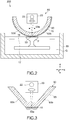
Fig. 2 is a diagram showing a structure of amolding apparatus 200 according to an example 1 of the embodiment 2. Theoptical head unit 80 includes aregulation body 50 and thelight irradiation section 20 having thelight source 22. For example, thelight irradiation section 20 and theregulation body 50 are integrally supported by a support member or a connecting member (not shown) and is configured to be capable of integrally moving by the x movement mechanism 31 (seeFig. 1 ). - The
photocatalyst layer 15 is arranged on thesurface 53 that is an outer surface of theregulation body 50. Thesurface 53 includes aregulation surface 53a and anarea 53b other than that. Theregulation body 50 is configured such that theregulation surface 53a is arranged at the position closer to thestage 17 than thearea 53b other than the regulation surface. Specifically, theregulation surface 53a including thesurface 53 has a curved surface. For example, theregulation body 50 has a part of a cylindrical shape, e.g., a half cylindrical shape. - The
light irradiation section 20 irradiates a material with light in a one-dimensional slit area between theregulation surface 53a and the stage 17 (or cured layer on stage 17). The one-dimensional direction is an axial direction of the semicylindrical regulation body 50, i.e., a direction along the y axis. - In this embodiment, the regulation range of the material is limited to the
regulation surface 53a as narrow as possible. This allows a surface area of a contact area between the cured layer and theregulation surface 53a to be small and a contraction force when the material is cured has a small impact on theregulation surface 53a. As a result, it becomes possible to produce the molded object P with high accuracy. In addition, since the contact area is small, the cured material can be peeled more easily, the molding speed is increased, and the yield is increased. -
Fig. 3 is a diagram showing a structure of a molding apparatus according to an example 2 of an embodiment 2. Aregulation body 90 has a triangle shape or a trapezoid shape. Asurface 93 that is an outer surface of theregulation body 90 has aregulation surface 93a arranged so as to be closest to the stage and anarea 93b other than that. At least, theregulation surface 93a has a flat surface. Thephotocatalyst layer 15 is arranged only on theregulation surface 93a, but thephotocatalyst layer 15 may be arranged on an entire surface of thesurface 93. - Also, with the molding apparatus according to the example 2, the effects similar to the above-described example 1 can be provided.
-
Fig. 4 is an enlarged cross-sectional diagram showing a photocatalyst layer according to an embodiment 3 as other embodiment. Aphotocatalyst layer 55 of aregulation body 130 includes a multi-layer structure made of a plurality of different materials. Thephotocatalyst layer 15 includes titanium oxide and tantalum oxide alternately arranged, for example. The number of layers is 3 or more. For example, there are several layers to twenty layers. - Since refractive indices of materials in the respective layers are different, light transmittance of the
photocatalyst layer 55 can be controlled by the number of layers and the thickness of each layer. According to this structure, an amount of gas generated by light irradiation can be controlled. As a result, a force needed for peeling can be selectively designed. - The present technology is not limited to the above-described embodiments. For example, in the above-described embodiment 2, the
light irradiation section 20 and theregulation body 50 are integrally supported. However, these may not necessarily be integrated and may be configured to be moved by separate movement mechanisms. - In the above-described each embodiment, instead of moving the
optical head unit x movement mechanism 31, the movement mechanism of thestage 17 may be configured to move thestage 17 not only in the z direction but in the x direction. - In the embodiment 2, the regulation body has a cylindrical shape, a trapezoid shape, or the like. However, the surface of the regulation body may be a quadric surface such as an oval surface and a paraboloid surface or may be a combined surface of a curved surface and a planar surface.
- The
light irradiation section 20 includes the line light source as thelight source 22. However, the light irradiation section may include a point light source and may have a mechanism that scan light from the point light source on a material in the y direction. - It is possible to combine at least two features of the respective embodiments described above.
- The present technology may also have the following structures.
- (1) A molding apparatus, including:
- a stage having a stage surface;
- a regulation body having a surface including a regulation surface facing to the stage surface and a photocatalyst layer arranged on the regulation surface, the regulation body regulating a position in a lamination direction of a material of a molded object to be formed on the stage surface by the regulation surface;
- a light irradiation section that irradiates the material with light via the photocatalyst layer of the regulation body; and
- a movement mechanism that relatively moves the stage and the regulation body.
- (2) The molding apparatus according to (1), in which
the regulation surface is a planar surface. - (3) The molding apparatus according to (1), in which
the surface further includes an area other than the regulation surface,
the regulation surface is configured such that the regulation surface is arranged at a position closer to the stage than the area other than the regulation surface, and
the photocatalyst layer is arranged on at least the regulation surface. - (4) The molding apparatus according to (3), in which
the light irradiation section irradiates the material in a one-dimensional slit area between the regulation surface and the stage with light. - (5) The molding apparatus according to any one of (1) to (4), in which
the photocatalyst layer includes a multi-layer structure made of a plurality of different materials. - (6) The molding apparatus according to any one of (1) to (5), in which
the photocatalyst layer includes at least one of titanium oxide or tantalum oxide. - (7) The molding apparatus according to any one of (1) to (6), in which
the light irradiation section irradiates with light having a wavelength of 450 nm or less. - (8) The molding apparatus according any one of (1) to (7), in which
a surface roughness of the photocatalyst layer is 100 µm or less. - (9) An optical head unit used for a molding apparatus that includes a stage having a stage surface and the optical head unit arranged facing to the stage, including:
- a regulation body having a surface including a regulation surface facing to the stage surface and a photocatalyst layer arranged on the regulation surface, the regulation body regulating a position in a lamination direction of a material of a molded object to be formed on the stage surface by the regulation surface; and
- a light irradiation section that irradiates the material with light via the photocatalyst layer of the regulation body.
-
- 10, 50, 90, 130
- regulation body
- 13
- regulation surface
- 15, 55
- photocatalyst layer
- 17
- stage
- 18
- stage surface
- 20
- light irradiation section
- 31
- x movement mechanism
- 32
- z movement mechanism
- 40, 80
- optical head unit
- 53, 93
- surface
- 53a, 93a
- regulation surface
- 53b, 93b
- area other than regulation surface
- 100, 200
- molding apparatus
Claims (9)
- A molding apparatus, comprising:a stage having a stage surface;a regulation body having a surface including a regulation surface facing to the stage surface and a photocatalyst layer arranged on the regulation surface, the regulation body regulating a position in a lamination direction of a material of a molded object to be formed on the stage surface by the regulation surface;a light irradiation section that irradiates the material with light via the photocatalyst layer of the regulation body; anda movement mechanism that relatively moves the stage and the regulation body.
- The molding apparatus according to claim 1, wherein
the regulation surface is a planar surface. - The molding apparatus according to claim 1, wherein
the surface further includes an area other than the regulation surface,
the regulation surface is configured such that the regulation surface is arranged at a position closer to the stage than the area other than the regulation surface, and
the photocatalyst layer is arranged on at least the regulation surface. - The molding apparatus according to claim 3, wherein
the light irradiation section irradiates the material in a one-dimensional slit area between the regulation surface and the stage with light. - The molding apparatus according to claim 1, wherein
the photocatalyst layer includes a multi-layer structure made of a plurality of different materials. - The molding apparatus according to claim 1, wherein
the photocatalyst layer includes at least one of titanium oxide or tantalum oxide. - The molding apparatus according to claim 1, wherein
the light irradiation section irradiates with light having a wavelength of 450 nm or less. - The molding apparatus according to claim 1, wherein
a surface roughness of the photocatalyst layer is 100 µm or less. - An optical head unit used for a molding apparatus that includes a stage having a stage surface and the optical head unit arranged facing to the stage, comprising:a regulation body having a surface including a regulation surface facing to the stage surface and a photocatalyst layer arranged on the regulation surface, the regulation body regulating a position in a lamination direction of a material of a molded object to be formed on the stage surface by the regulation surface; anda light irradiation section that irradiates the material with light via the photocatalyst layer of the regulation body.
Applications Claiming Priority (2)
| Application Number | Priority Date | Filing Date | Title |
|---|---|---|---|
| JP2017119321 | 2017-06-19 | ||
| PCT/JP2018/014587 WO2018235387A1 (en) | 2017-06-19 | 2018-04-05 | Modeling device and optical head unit |
Publications (2)
| Publication Number | Publication Date |
|---|---|
| EP3643478A1 true EP3643478A1 (en) | 2020-04-29 |
| EP3643478A4 EP3643478A4 (en) | 2020-06-24 |
Family
ID=64737004
Family Applications (1)
| Application Number | Title | Priority Date | Filing Date |
|---|---|---|---|
| EP18819965.7A Withdrawn EP3643478A4 (en) | 2017-06-19 | 2018-04-05 | MODELING DEVICE AND OPTICAL HEAD UNIT |
Country Status (6)
| Country | Link |
|---|---|
| US (1) | US20200198237A1 (en) |
| EP (1) | EP3643478A4 (en) |
| JP (1) | JP7092125B2 (en) |
| CN (1) | CN110809512A (en) |
| TW (1) | TW201904750A (en) |
| WO (1) | WO2018235387A1 (en) |
Family Cites Families (11)
| Publication number | Priority date | Publication date | Assignee | Title |
|---|---|---|---|---|
| JPH1034668A (en) * | 1996-07-25 | 1998-02-10 | Toto Ltd | Molding die |
| JP2002036373A (en) * | 2000-07-25 | 2002-02-05 | Sanyo Electric Co Ltd | Stereolithography |
| JP2007144995A (en) * | 2005-10-25 | 2007-06-14 | Dainippon Printing Co Ltd | Mold for photo-curing nanoimprint and method for producing the same |
| JP2008221491A (en) | 2007-03-09 | 2008-09-25 | Dainippon Printing Co Ltd | Nanoimprint mold and manufacturing method thereof |
| JP5045402B2 (en) | 2007-12-04 | 2012-10-10 | ソニー株式会社 | Stereolithography equipment |
| JP5088114B2 (en) | 2007-12-04 | 2012-12-05 | ソニー株式会社 | Stereolithography equipment |
| US9636873B2 (en) * | 2012-05-03 | 2017-05-02 | B9Creations, LLC | Solid image apparatus with improved part separation from the image plate |
| WO2014126834A2 (en) * | 2013-02-12 | 2014-08-21 | Eipi Systems, Inc. | Method and apparatus for three-dimensional fabrication with feed through carrier |
| EP2969482B1 (en) * | 2013-03-15 | 2018-05-09 | 3D Systems, Inc. | Three dimensional printing material system |
| US10308007B2 (en) * | 2015-06-18 | 2019-06-04 | University Of Southern California | Mask video projection based stereolithography with continuous resin flow |
| US10935891B2 (en) * | 2017-03-13 | 2021-03-02 | Holo, Inc. | Multi wavelength stereolithography hardware configurations |
-
2018
- 2018-04-05 WO PCT/JP2018/014587 patent/WO2018235387A1/en not_active Ceased
- 2018-04-05 EP EP18819965.7A patent/EP3643478A4/en not_active Withdrawn
- 2018-04-05 CN CN201880039146.3A patent/CN110809512A/en active Pending
- 2018-04-05 JP JP2019525127A patent/JP7092125B2/en not_active Expired - Fee Related
- 2018-04-05 US US16/620,920 patent/US20200198237A1/en not_active Abandoned
- 2018-04-25 TW TW107113951A patent/TW201904750A/en unknown
Also Published As
| Publication number | Publication date |
|---|---|
| CN110809512A (en) | 2020-02-18 |
| TW201904750A (en) | 2019-02-01 |
| US20200198237A1 (en) | 2020-06-25 |
| WO2018235387A1 (en) | 2018-12-27 |
| JPWO2018235387A1 (en) | 2020-04-16 |
| EP3643478A4 (en) | 2020-06-24 |
| JP7092125B2 (en) | 2022-06-28 |
Similar Documents
| Publication | Publication Date | Title |
|---|---|---|
| JP6233001B2 (en) | Modeling apparatus and method for manufacturing modeled object | |
| JP6567969B2 (en) | Three-dimensional complex multilayer structure and manufacturing method thereof | |
| KR101093026B1 (en) | Laser module | |
| JP6038787B2 (en) | Manufacturing method of optical waveguide | |
| CN1580824A (en) | Micro lens and making method thereof, optical device, optical transmitting device and head for laser printer | |
| KR20130133293A (en) | Convexo-concave microstructure transcription template | |
| Kunwar et al. | Oxygen-permeable films for continuous additive, subtractive, and hybrid additive/subtractive manufacturing | |
| Lambert et al. | Design considerations for mask projection microstereolithography systems | |
| EP3643478A1 (en) | Modeling device and optical head unit | |
| JP2009300507A (en) | Diffraction lens, method and apparatus of manufacturing the same | |
| US7844157B2 (en) | Optical waveguide for luminescent device and manufacturing method thereof | |
| JP2009054784A (en) | Auxiliary plate and exposure apparatus having the same | |
| CN1284982C (en) | Color filter substrate, liquid crystal display device, electronic device, and manufacturing method thereof | |
| US8828755B2 (en) | Light-emitting element package and fabrication method thereof | |
| CN102590943A (en) | Optical waveguide production method | |
| CN109228315B (en) | Continuous 3D printing system | |
| JP2005156989A (en) | Lens barrel | |
| TW202108353A (en) | High-speed photocuring 3D printing system and method for enhancing uniformity of ultraviolet of 3D printing system capable of enhancing heat dissipation and improving energy utilization | |
| Choi et al. | Optimization of the projection microstereolithography process for a photocurable biomass-based resin | |
| Shiba et al. | UV-LED lithography system and characterization | |
| CN212783511U (en) | Brightness enhancement film | |
| Glauche et al. | Hot Embossing to Fabricate Parylene-Based Microstructures and Its Impact on the Material Properties | |
| CN114335375A (en) | Brightness enhancement film | |
| US20130333834A1 (en) | Manufacturing method of display | |
| JP2015002087A (en) | Semiconductor light-emitting element, organic el element, and method of manufacturing semiconductor light-emitting element |
Legal Events
| Date | Code | Title | Description |
|---|---|---|---|
| STAA | Information on the status of an ep patent application or granted ep patent |
Free format text: STATUS: THE INTERNATIONAL PUBLICATION HAS BEEN MADE |
|
| PUAI | Public reference made under article 153(3) epc to a published international application that has entered the european phase |
Free format text: ORIGINAL CODE: 0009012 |
|
| STAA | Information on the status of an ep patent application or granted ep patent |
Free format text: STATUS: REQUEST FOR EXAMINATION WAS MADE |
|
| 17P | Request for examination filed |
Effective date: 20191112 |
|
| AK | Designated contracting states |
Kind code of ref document: A1 Designated state(s): AL AT BE BG CH CY CZ DE DK EE ES FI FR GB GR HR HU IE IS IT LI LT LU LV MC MK MT NL NO PL PT RO RS SE SI SK SM TR |
|
| AX | Request for extension of the european patent |
Extension state: BA ME |
|
| A4 | Supplementary search report drawn up and despatched |
Effective date: 20200525 |
|
| RIC1 | Information provided on ipc code assigned before grant |
Ipc: B29C 64/20 20170101AFI20200516BHEP Ipc: B29C 64/286 20170101ALI20200516BHEP Ipc: B33Y 30/00 20150101ALI20200516BHEP Ipc: B29C 64/135 20170101ALI20200516BHEP Ipc: B29C 64/264 20170101ALI20200516BHEP |
|
| DAV | Request for validation of the european patent (deleted) | ||
| DAX | Request for extension of the european patent (deleted) | ||
| RAP3 | Party data changed (applicant data changed or rights of an application transferred) |
Owner name: SONY GROUP CORPORATION |
|
| STAA | Information on the status of an ep patent application or granted ep patent |
Free format text: STATUS: THE APPLICATION HAS BEEN WITHDRAWN |
|
| 18W | Application withdrawn |
Effective date: 20210810 |