EP3640942A1 - Ferromagnetic tunnel junction, spintronics device using same, and method for manufacturing ferromagnetic tunnel junction - Google Patents
Ferromagnetic tunnel junction, spintronics device using same, and method for manufacturing ferromagnetic tunnel junction Download PDFInfo
- Publication number
- EP3640942A1 EP3640942A1 EP18816984.1A EP18816984A EP3640942A1 EP 3640942 A1 EP3640942 A1 EP 3640942A1 EP 18816984 A EP18816984 A EP 18816984A EP 3640942 A1 EP3640942 A1 EP 3640942A1
- Authority
- EP
- European Patent Office
- Prior art keywords
- layer
- magnetic
- insulating layer
- tunnel junction
- film
- Prior art date
- Legal status (The legal status is an assumption and is not a legal conclusion. Google has not performed a legal analysis and makes no representation as to the accuracy of the status listed.)
- Granted
Links
Images



Classifications
-
- H—ELECTRICITY
- H10—SEMICONDUCTOR DEVICES; ELECTRIC SOLID-STATE DEVICES NOT OTHERWISE PROVIDED FOR
- H10N—ELECTRIC SOLID-STATE DEVICES NOT OTHERWISE PROVIDED FOR
- H10N50/00—Galvanomagnetic devices
- H10N50/80—Constructional details
-
- G—PHYSICS
- G11—INFORMATION STORAGE
- G11B—INFORMATION STORAGE BASED ON RELATIVE MOVEMENT BETWEEN RECORD CARRIER AND TRANSDUCER
- G11B5/00—Recording by magnetisation or demagnetisation of a record carrier; Reproducing by magnetic means; Record carriers therefor
- G11B5/127—Structure or manufacture of heads, e.g. inductive
- G11B5/33—Structure or manufacture of flux-sensitive heads, i.e. for reproduction only; Combination of such heads with means for recording or erasing only
- G11B5/39—Structure or manufacture of flux-sensitive heads, i.e. for reproduction only; Combination of such heads with means for recording or erasing only using magneto-resistive devices or effects
- G11B5/3903—Structure or manufacture of flux-sensitive heads, i.e. for reproduction only; Combination of such heads with means for recording or erasing only using magneto-resistive devices or effects using magnetic thin film layers or their effects, the films being part of integrated structures
- G11B5/3906—Details related to the use of magnetic thin film layers or to their effects
- G11B5/3909—Arrangements using a magnetic tunnel junction
-
- G—PHYSICS
- G11—INFORMATION STORAGE
- G11C—STATIC STORES
- G11C11/00—Digital stores characterised by the use of particular electric or magnetic storage elements; Storage elements therefor
- G11C11/02—Digital stores characterised by the use of particular electric or magnetic storage elements; Storage elements therefor using magnetic elements
- G11C11/16—Digital stores characterised by the use of particular electric or magnetic storage elements; Storage elements therefor using magnetic elements using elements in which the storage effect is based on magnetic spin effect
- G11C11/161—Digital stores characterised by the use of particular electric or magnetic storage elements; Storage elements therefor using magnetic elements using elements in which the storage effect is based on magnetic spin effect details concerning the memory cell structure, e.g. the layers of the ferromagnetic memory cell
-
- H—ELECTRICITY
- H10—SEMICONDUCTOR DEVICES; ELECTRIC SOLID-STATE DEVICES NOT OTHERWISE PROVIDED FOR
- H10B—ELECTRONIC MEMORY DEVICES
- H10B61/00—Magnetic memory devices, e.g. magnetoresistive RAM [MRAM] devices
-
- H—ELECTRICITY
- H10—SEMICONDUCTOR DEVICES; ELECTRIC SOLID-STATE DEVICES NOT OTHERWISE PROVIDED FOR
- H10B—ELECTRONIC MEMORY DEVICES
- H10B61/00—Magnetic memory devices, e.g. magnetoresistive RAM [MRAM] devices
- H10B61/20—Magnetic memory devices, e.g. magnetoresistive RAM [MRAM] devices comprising components having three or more electrodes, e.g. transistors
-
- H—ELECTRICITY
- H10—SEMICONDUCTOR DEVICES; ELECTRIC SOLID-STATE DEVICES NOT OTHERWISE PROVIDED FOR
- H10N—ELECTRIC SOLID-STATE DEVICES NOT OTHERWISE PROVIDED FOR
- H10N50/00—Galvanomagnetic devices
- H10N50/01—Manufacture or treatment
-
- H—ELECTRICITY
- H10—SEMICONDUCTOR DEVICES; ELECTRIC SOLID-STATE DEVICES NOT OTHERWISE PROVIDED FOR
- H10N—ELECTRIC SOLID-STATE DEVICES NOT OTHERWISE PROVIDED FOR
- H10N50/00—Galvanomagnetic devices
- H10N50/10—Magnetoresistive devices
-
- H—ELECTRICITY
- H10—SEMICONDUCTOR DEVICES; ELECTRIC SOLID-STATE DEVICES NOT OTHERWISE PROVIDED FOR
- H10N—ELECTRIC SOLID-STATE DEVICES NOT OTHERWISE PROVIDED FOR
- H10N50/00—Galvanomagnetic devices
- H10N50/80—Constructional details
- H10N50/85—Materials of the active region
-
- G—PHYSICS
- G01—MEASURING; TESTING
- G01R—MEASURING ELECTRIC VARIABLES; MEASURING MAGNETIC VARIABLES
- G01R33/00—Arrangements or instruments for measuring magnetic variables
- G01R33/02—Measuring direction or magnitude of magnetic fields or magnetic flux
- G01R33/06—Measuring direction or magnitude of magnetic fields or magnetic flux using galvano-magnetic devices
- G01R33/09—Magnetoresistive devices
- G01R33/098—Magnetoresistive devices comprising tunnel junctions, e.g. tunnel magnetoresistance sensors
Definitions
- An embodiment of the invention relates to a magnetic tunnel junction, a spintronics device (a magneto-resistance effect element and a magnetic memory device) using the magnetic tunnel junction, and a method for manufacturing a magnetic tunnel junction.
- a magnetic tunnel junction that is made of a three-layer structure of a ferromagnetic layer/insulator layer (barrier layer)/ferromagnetic layer is used as, for example, the magnetic head of a hard disk device or the information recording cell of nonvolatile random access memory (MRAM: Magneto-resistive random access memory). Also, utilization is possible as a compact highly-sensitive magnetic sensor.
- a MTJ element has a tunnel magneto-resistance effect (TMR: Tunnel magneto-resistance) in which the tunnel resistance value changes via a barrier layer according to the relative magnetization angles of two ferromagnetic layers. In such a field of application, it is desirable to have a high magneto-resistance change ratio (TMR ratio), to be easy to make, and to be makeable on a wide range of substrates.
- a MTJ element that is made of cobalt-iron-boron (CoFeB) as a ferromagnetic layer and magnesium oxide (MgO) as a barrier layer is widely used.
- CoFeB cobalt-iron-boron
- MgO magnesium oxide
- the major reason thereof is because CoFeB is amorphous; therefore, there are favorable features for a wide range of element applications such as a high TMR ratio exceeding 100% being obtained relatively easily at room temperature, a MTJ element structure being directly makeable on a wide range of underlayer structures, etc.
- the high TMR ratio is caused by the crystallization of the CoFeB layer progressing from the MgO barrier layer.
- a film of MgO that is formed on the amorphous CoFeB layer by using sputtering, etc., is obtained as a layer having (001) orientation-growth; crystallization of the CoFeB layer progresses from the MgO layer-side interface due to heat treatment at about 200 to 500 °C; and as a result, a high-quality interface crystal structure is realized. Therefore, in the MTJ element that has a CoFeB/MgO/CoFeB structure, a stacked structure in which all three layers have the (001) crystal orientation is realized by the heat treatment; therefore, a large increase of the TMR ratio is observed (Non-Patent Literature 1). The high TMR ratio is due to a coherent tunneling effect via the ⁇ 1 -band of the MgO (001).
- MgAl 2 O 4 As a method for making a higher-quality MTJ element by reducing such a large lattice mismatch, there is a method of using MgAl 2 O 4 as the barrier layer (Patent Literature 1).
- MgAl 2 O 4 has a spinel structure having a lattice constant of about 0.809 nm as a stable structure.
- the crystal lattice spacing has good lattice matching with a wide range of ferromagnets such as CoFeB, CoFe, Co-based Heusler alloys, FePt, CoPt, MnGa, MnGe, etc., because the crystal lattice spacing is about 4% smaller than MgO which has a rock-salt structure.
- MgAl 2 O 4 it is unnecessary for the ratio of Mg and Al to be 1: 2 which is the stoichiometric ratio; the lattice constant can be changed continuously by adjusting the ratio of Mg and Al; therefore, the lattice matching with the ferromagnetic layer can be increased further. Therefore, a more general representation of MgAl 2 O 4 can be written as (Mg 1- x Al x )-O x (0 ⁇ x ⁇ 1).
- Patent Literature 2 In the case where a MgAl 2 O 4 barrier layer is used as well, the coherent effect arises; and a large TMR ratio exceeding 300% at room temperature is realized (Patent Literature 2). Also, a problem is known in which the TMR ratio decreases due to the application of a bias voltage in a MTJ element; and this is a practical problem (bias voltage dependence). It is also known that the degree of the decrease of the TMR ratio can be reduced if the lattice mismatch is reduced by introducing the MgAl 2 O 4 barrier layer (Patent Literature 1).
- Patent Literature 3 a perpendicular magnetization MTJ element that is suited to increasing the capacity of MRAM can be configured.
- Non-Patent Literature 2 and Non-Patent Literature 3 there was a problem in which an amorphous MgAl 2 O 4 layer is obtained if the MgAl 2 O 4 layer is formed on amorphous CoFeB; therefore, the crystallization of the MTJ element cannot be realized; therefore, the coherent tunneling effect is not obtained; and a high TMR ratio such as a TMR ratio exceeding 100% cannot be realized using the CoFeB layer and the MgAl 2 O 4 barrier layer.
- the invention is directed to achieve a high TMR ratio by realizing a MTJ element including a CoFeB layer and a MgAl 2 O 4 barrier layer without using a conventional single-crystal underlayer. It is also directed to suppress the bias voltage dependence of the TMR ratio.
- the inventors discovered that by forming a MgAl 2 O 4 film after forming extremely thin MgO on a CoFeB layer, crystallization of the MgAl 2 O 4 layer occurs; and a MgO/MgAl 2 O 4 stacked film is obtained as an oriented film having (001) growth.
- the inventors discovered that all of the layers of the stacked film made of the CoFeB/MgO/MgAl 2 O 4 /CoFeB structure are crystallized by heat treatment so that the stacked film functions as a MTJ element realizing a high TMR ratio.
- the discovery that the bias voltage dependence is improved by the effect of the MgO/MgAl 2 O 4 stacked barrier layer having a small lattice mismatch with CoFeB also led to the invention.
- a barrier layer that is made of Mg-Al-O having a small lattice mismatch with CoFeB is provided; and as a result, for example, a MTJ element in which a large TMR ratio is obtained and a method for making the MTJ element are provided.
- a large TMR ratio is the obtainment of a TMR ratio of 120% or more at room temperature.
- the MTJ element of the invention not only is applicable to a hard disk magnetic head and a spin torque rewritable MRAM (a STT-MRAM), but also can be utilized in many spintronics devices such as a three-terminal MRAM, a voltage-driven MRAM, a spin torque oscillator, a spin resonance tunnel element, etc.
- a STT-MRAM spin torque rewritable MRAM
- FIG. 1A, FIG. 1B, FIG. 2A, and FIG. 2B The tunnel barrier of the embodiment and embodiments of MTJ elements using the tunnel barrier will now be described with reference to FIG. 1A, FIG. 1B, FIG. 2A, and FIG. 2B .
- the MTJ element of the embodiment is an element in which a first magnetic layer, a first insulating layer, a second insulating layer, and a second magnetic layer are stacked in this order on a substrate.
- the first insulating layer and the second insulating layer are made of oxides.
- the first magnetic layer and the second magnetic layer are made of CoFeB; and the first insulating layer and the second insulating layer respectively have MgO and MgAl 2 O 4 as major bodies.
- the Mg: Al ratio of MgAl 2 O 4 it is unnecessary for the Mg: Al ratio of MgAl 2 O 4 to be 1: 2 in the second insulating layer; and compositions having a wide range of ratios can be used (hereinafter, recited using the general notation of Mg-AI-O).
- both a spinel structure and a cation-disordered spinel structure can be used as the crystal structure of Mg-AI-O.
- the elements that form the spinel structure may include, for example, an oxide including Li and Zn.
- the first insulating layer may have a stacked structure of a metal Mg layer/MgO layer or a structure including a small amount of Al or Ti. Also, the effects also are realized in a structure in which a CoFe alloy is inserted between the first magnetic layer and the first insulating layer and/or between the second magnetic layer and the second insulating layer.
- a MTJ film first embodiment 101 which is the basic structure of a first embodiment is shown in FIG. 1A .
- the MTJ film first embodiment 101 has a multilayer film structure; and a first magnetic layer 1, a first insulating layer 11, a second insulating layer 12, and a second magnetic layer 2 are stacked in order from the bottom.
- Either of the first magnetic layer 1 and the second magnetic layer 2 may be a fixed magnetic layer or a free magnetic layer.
- the magnetization direction may be either a film in-plane direction or a film out-of-plane direction.
- the first magnetic layer 1 is, for example, a layer made of Co-Fe-B formed by physical vapor deposition such as sputtering, vapor deposition, etc.
- the Co-Fe-B has an amorphous structure at this stage. It is sufficient for the composition of Co and Fe to be Co 1- n Fe n (0 ⁇ n ⁇ 1); and the composition of Co and Fe is a composition that includes CoB and FeB. It is sufficient for the B composition inside Co-Fe-B to be in a range in which the Co-Fe-B layer is ferromagnetic and amorphous; and the B composition in Co-Fe-B is, for example, about 15 to 25 atomic%.
- this layer is, for example, 0.8 to 5 nm but is determined to be in balance with the lower layer structure of the first magnetic layer 1. Also, this layer also can be obtained as a layer having perpendicular magnetization by setting this layer to be extremely thin with a thickness of not more than about 1.5 nm.
- the first insulating layer 11 is a layer made of an oxide having MgO as a major body.
- the oxygen amount may be somewhat deficient or excessive; and effects are obtained in the range of MgO 1+ ⁇ (-0.2 ⁇ ⁇ ⁇ 0.2).
- This layer can be utilized because this layer is obtained as a crystal layer even if Al or Ti is included at about 15 atomic% with respect to Mg.
- the first insulating layer 11 has the effect of promoting the crystallization of the second insulating layer 12 formed on the first insulating layer 11 and is a crystal film having substantially (001) growth, but may partially include amorphous and/or polycrystalline bodies at this stage.
- heat treatment in a vacuum at a range of about 100 to 400 °C also can be performed after the formation of this layer.
- the second insulating layer 12 is a hybrid oxide layer having Mg-Al-O as a major component.
- This layer can have a cubic crystal body.
- the composition is such that a spinel structure is the stable structure.
- Mg 1- y Al y (0.2 ⁇ y ⁇ 0.8) can be used as the composition of Mg and Al.
- y is set to be 0.2 or more to obtain the effect of improving V half , because the lattice mismatch between the first magnetic body 1 and the second magnetic body 2 can be reduced to be about 3% or less.
- y is set to be 0.8 or less because the crystallization of Mg-Al-O becomes difficult due to the effect of the Al-rich composition. Also, the effects are obtained even if the oxygen amount of this layer is deficient or excessive with respect to the stoichiometric composition; for example, as a general formula, a range of Mg 1- x Al x O 1.5- x /2+ ⁇ ' (-0.2 ⁇ ⁇ ' ⁇ 0.2) can be utilized. Also, a portion of Mg and Al may be replaced with Zn and Li with the object of stabilizing the spinel structure, adjusting the insulative characteristics and the element resistance, and/or improving the TMR ratio.
- the Al oxides of ZnAl 2 O 4 and LiAl 2.5 O 4 that include Zn and Li are insulating bodies having spinel structure crystals having about the same lattice constant as MgAl 2 O 4 .
- the effects of the embodiment are realized even if Zn and Li are included because a solid solution that is continuous with MgAl 2 O 4 can be made due to the feature of these material properties being similar.
- heat treatment in a vacuum at the range of 100 to 400 °C also can be performed after the formation of this layer.
- first insulating layer 11 and the second insulating layer 12 can be made using various known methods. For example, high frequency sputtering from a target material made of an oxide, reactive vapor deposition or reactive sputtering using an oxygen gas, a method of oxidizing after forming a metal layer made of an alloy of Mg or Mg 1- a Al a (0 ⁇ a ⁇ 1) (post oxidation), multistep post oxidation, or a technique in which these techniques are combined can be used. These techniques may be performed while heating the substrate at a temperature in a range that does not degrade the flatness.
- the range of 0.05 to 1.2 nm is favorable as the thickness of the first insulating layer 11.
- 0.1 to 1.0 nm is more favorable.
- 0.2 to 0.8 nm is more favorable.
- 0.05 nm corresponds to the thickness of about 1/4 of one atomic plane of MgO (001); and this thickness or more can function as a crystal template for obtaining the second insulating layer 12 as a crystal layer.
- the crystal template effect improves; and the crystallization of the second insulating layer 12 can be realized at a lower heat treatment temperature.
- the thickness is not limited in terms of crystallizing the second insulating layer 12, to provide a practical resistance area (resistance R ⁇ area A ; the RA value) as the MTJ element, it is favorable for the thickness to be 3 nm or less; and it is more favorable for the thickness to be 2 nm or less.
- R ⁇ area A resistance area
- the second insulating layer 12 film thickness it is favorable for the second insulating layer 12 film thickness to be equal to or greater than the first insulating layer 11 layer thickness.
- the total thickness of the stacked film of the first insulating layer and the second insulating layer to be 0.6 nm to 3 nm.
- control of the interface crystal structure and/or the adjustment of the perpendicular magnetic anisotropy also can be performed by inserting an extremely thin metal film made of Mg 1- b Al b (0 ⁇ b ⁇ 1) and having a thickness of, for example, 1 nm or less between the first magnetic layer 1 and the first insulating layer 11 and/or between the second insulating layer 12 and the second magnetic layer 2.
- the second magnetic layer 2 is formed on the second insulating layer 12.
- the second magnetic layer 2 also is a layer having an amorphous structure and having Co-Fe-B as a major body.
- the same technique as the first magnetic layer 1 can be used as the method for making the layer.
- the structure After forming the multilayer film structure recited above, for example, by performing heat treatment in a vacuum for 1 minute to 60 minutes at a temperature range of about 200 to 500 °C, the structure changes to a cubic structure as an entirety; and a crystal multilayer film that has substantially the (001) orientation is formed.
- mutual atomic diffusion can be promoted partially or as an entirety in the first insulating layer 11 and the second insulating layer 12; and one body of a Mg-Al-O barrier layer also can be obtained.
- a magnetic tunnel junction that has a tunnel magneto-resistance not less than 120% and not more than 34000% at room temperature is made.
- a second embodiment is shown as a MTJ film second embodiment 201 in FIG. 1B and will now be described.
- the MTJ film second embodiment 201 is the MTJ film first embodiment 101 in which a magnetic insertion layer 3 is newly provided between the first magnetic layer 1 and the first insulating layer 11. Otherwise, a structure, a composition, and a manufacturing method equivalent to those of the MTJ film first embodiment 101 can be used.
- the magnetic insertion layer 3 is a thin insertion layer made of Co 1- m Fe m (0 ⁇ m ⁇ 1).
- the magnetic insertion layer 3 has the effect of promoting the crystallization of both the first insulating layer 11 and the second insulating layer 12, and causes the improvement of the TMR ratio.
- the magnetic insertion layer 3 can be made using the same technique as Co-Fe-B such as sputtering, vacuum vapor deposition, etc. To improve the flatness of the magnetic insertion layer 3, heat treatment may be performed in a vacuum at a temperature of 100 to 300 °C. Also, a CoFe alloy layer may be inserted using a technique similar to that of the magnetic insertion layer 3 also between the second insulating layer 12 and the second magnetic layer 2.
- a third embodiment is the MTJ film first embodiment 101 in which a lower structure of the first magnetic layer 1 and an upper structure of the second magnetic layer 2 are newly provided.
- a substrate 21 is provided; and an underlayer structure layer 22 is provided on the substrate 21.
- the MTJ film first embodiment 101 is provided on the underlayer structure layer 22.
- an upper structure layer 23 is provided on the MTJ film first embodiment 101.
- the substrate 21 it is desirable for the substrate 21 to be flat and homogeneous.
- a Si-based material such as Si, Si having a thermal oxide film (Si/SiO 2 ), SiN, SiC, etc., a compound semiconductor such as GaAs, etc., or an oxide crystal such as MgO, MgAl 2 O 4 , sapphire, etc., can be used.
- the underlayer structure layer 22 is provided between the substrate 21 and the first magnetic layer 1, is used as an electrode layer on the lower side, and is used for controlling the magnetic properties and/or the crystal structure of the first magnetic layer.
- a known multilayer structure can be utilized in the underlayer structure layer 22.
- the electrode layer a layer that includes at least one selected from the group consisting of Ta, TaN, Ru, Ir, Pt, W, Ti, TiN, AITiC, Cu, CuN, Mo, Cr, Au, Ag, NiAl, NiFe, IrMn, and PtMn can be used.
- an oxide layer of MgO, MgAl 2 O 4 , AlO x , SiO x , SrTiO 3 , etc., may be included between the electrode layer and the substrate 21. These oxide layers can be used for controlling the crystal orientation of the electrode layer.
- a magnetic layer may be included between the electrode layer and the first magnetic layer 1; for example, Co-Fe alloys, Co-Fe-Tb alloys, Mn-Ga alloys, Mn-Ge alloys, Mn-Ga-N, Fe-Pt alloys, Co-Pt alloys, etc., or a stacked film of these alloys may be used. Also, Co-based Heusler alloys that are represented by Co 2 YZ (Y being Fe, Mn, Ti, V, Cr, etc., and Z being Al, Si, Sn, Ga, Ge, etc.) also can be used.
- the structure may be a multilayer stack of a layer including at least one element selected from (Co or Fe) and a layer including at least one element selected from (Pt or Pd).
- a nonmagnetic layer of Ru, Ti, W, Mo, Ir, etc. may be inserted between the layers including these magnetic bodies. Heat treatment in a vacuum also can be performed for each of these layers.
- Examples of the stacking of the underlayer structure layer 22 are, from the bottom, a Ta (5 nm)/Ru (10 nm)/NiFe (5 nm)/IrMn (10 nm)/CoFe (2.5 nm)/Ru (0.8 nm)/CoFe (2 nm) structure, a Ta (5 nm)/Ru (10 nm)/Pt (3 nm)/[Co (0.2 nm)/Pt (0.4 nm)] multilayer film/Co (0.2 nm)/Ru (0.8 nm)/[Co (0.2 nm)/Pt (0.4 nm)] multilayer film/CoFeB (1 nm)/Ta (0.2 nm) structure, and a MgO (7 nm)/Cr (40 nm)/Co 2 FeAl (5 nm) structure.
- the film thickness is inside ().
- the upper structure film 23 is provided on the second magnetic layer 2.
- the upper structure film 23 functions as an upper electrode and as a protective film of the magnetic tunnel junction film as well.
- Ta 5 nm
- Ru 15 nm
- Ta has the property of absorbing a portion of the B of Co-Fe-B during the heat treatment, and as a result of being provided directly on the Co-Fe-B, also has the effect of promoting the crystallization of the Co-Fe-B layer.
- the structure of the underlayer structure layer 22 that includes the magnetic body may be included to control the magnetic properties and/or the crystal structure of the second magnetic layer 2.
- the structure is a Ta/CoFe/Ta/Ru structure or a W/[Co/Pd] multilayer film/Ta/Ru structure from the bottom.
- a thin oxide layer such as MgO, etc., may be included, e.g., a Ta/Co-Fe-B/MgO/Ta/Ru structure.
- a fourth embodiment is the MTJ film third embodiment 301 in which the magnetic insertion layer 3 is newly provided between the first magnetic layer 1 and the first insulating layer 11.
- the layer is a layer made of CoFe alloys and has the effect of promoting the crystallization of the first insulating layer 11 and the second insulating layer 12.
- a Si substrate having a thermal oxide film is used as a substrate, and is introduced to a sputtering apparatus after cleaning using isopropyl alcohol.
- a film of Ta (5 nm)/Co-Fe-B (5 nm) is formed at room temperature using magnetron sputtering.
- the Ta is an underlayer structure film; and the Co-Fe-B layer is the first magnetic layer.
- the composition of the target used in the formation of the Co-Fe-B layer is Co 20 Fe 60 B 20 .
- sputtering film formation of CoFe films of 0 (no insertion layer), 0.3, 0.6, and 0.9 nm was performed as a magnetic insertion layer.
- the target that was used has a Co 75 Fe 25 composition.
- a film of MgO (0.25 nm) was formed as the first insulating layer by high frequency sputtering using a MgO sintering target.
- a Mg-Al-O layer (10 nm) was formed by high frequency sputtering using a target having two different compositions.
- Mg-rich (Mg 0.67 Al 0.33 )-O x target was used; and the actual composition of Mg and Al of the Mg-Al-O layer was Mg 0.72 Al 0.28 by using inductively coupled plasma composition analysis.
- this composition is called Mg 2 Al-O x for convenience.
- the second composition an Al-rich (Mg 0.33 Al 0.67 )-O x target was used; and the actual composition of Mg and Al was Mg 0.39 Al 0.61 .
- this composition is called MgAl 2 -O x for convenience.
- a film of Co 20 Fe 60 B 20 (5 nm) was formed as the second magnetic layer on the Mg-Al-O layer; and a film of Ta (5 nm) was formed as an upper structure film on the second magnetic layer.
- heat treatment of the multilayer film structure that was made was performed in a vacuum for 30 minutes at 300 °C.
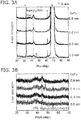
- FIG. 3A shows X-ray diffraction patterns obtained by scanning, in the film out-of-plane direction, the multilayer film structure in the case where the Mg-rich Mg 2 Al-O x is used.
- the patterns are shown separately for each CoFe insertion layer thickness.
- a peak that corresponds to MgAl 2 O 4 (004) is observed at the 42° vicinity. Other than this peak, it can be seen that there are only the peaks other than the substrate and the Ta layer.
- Mg 2 Al-O x layer is crystallized; and (001) growth is realized.
- the MgAl 2 O 4 (004) peak intensity increases as the CoFe insertion thickness increases. Accordingly, this shows that the insertion of the CoFe layer promotes the crystallization of MgAl 2 O 4 .
- FIG. 3B shows X-ray diffraction patterns obtained by scanning, in the film in-plane direction, the multilayer film structure of each CoFe insertion layer thickness.
- a peak that has MgAl 2 O 4 (400) and CoFe (110) as the origin is observed.
- the intensity of this peak also increases as the CoFe insertion layer thickness increases; therefore, it can be confirmed that there is a crystallization promotion effect of MgAl 2 O 4 due to the CoFe layer insertion.
- an ordered spinel structure of the Mg-Al-O layer was not observed. Therefore, it can be said that the structure is a cation-disordered spinel structure having a lattice constant that is half of the original lattice constant of MgAl 2 O 4 .
- the crystallization of a similar Mg-Al-O layer was confirmed from the X-ray diffraction pattern for the MgAl 2 -O x composition as well.
- the crystal lattice spacing in the film surface and in the film out-of-plane direction of the formed Mg-Al-O was estimated from the observed X-ray peak positions, the MgAl 2 O 4 (004) and (400).
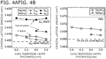
- FIG. 4A shows the relationship of the crystal lattice spacing with the CoFe insertion layer thickness for each of Mg 2 Al-O x and MgAl 2 -O x . From this figure, it can be seen that the lattice spacing substantially does not affect the CoFe film thickness for each of the compositions. Also, it can be seen that the lattice spacing in the film in-plane direction is smaller than the spacing in the film out-of-plane direction. The in-plane lattice spacing is in the range of 0.405 to 0.408 nm for each of the compositions.
- the crystal lattice volume is calculated in FIG. 4B .
- MgAl 2 -O x has a value near the bulk value (1/8 unit cell) of MgAl 2 O 4 converted to a value when the lattice constant is considered to be half.
- Mg 2 Al-O x has a value near the average value of the MgO bulk value and the MgAl 2 O 4 bulk converted value. Accordingly, this also suggests that continuous control of the crystal lattice volume is possible by adjusting the Mg-AI composition. It can also be seen that even for the Mg-rich composition which originally has lattice mismatch, in-plane lattice matching is realized by easily introducing tetragonal distortion.
- the Mg-Al-O layer is crystallized by inserting extremely thin MgO between the Mg-Al-O layer and the Co-Fe-B layer; and the crystallinity is improved further by the CoFe layer insertion. Also, it was also found that an in-plane lattice matching state with the Co-Fe-B layer can be realized for a wide range of compositions of Mg-AI.
- an example 2 will now be described using FIG. 5A, FIG. 5B , FIG. 6A, and FIG. 6 .
- an underlayer structure film of Ta (5 nm)/Ru (10 nm)/Ta (5 nm) was made on a Si substrate having a thermal oxide film.
- sputtering film formation of a Co 75 Fe 25 film was performed as a magnetic insertion layer.
- the film thickness of the Co 75 Fe 25 layer was changed in the range of 0.1 to 1.0 nm.
- a MgO layer was formed as the first insulating layer by changing the film thickness to be 0.1 to 0.8 nm.
- high frequency sputtering film formation of Mg 2 Al-O x or MgAl 2 -O x having a thickness of 1.2 nm was performed as the second insulating layer.
- a film of Co 20 Fe 60 B 20 (3 nm)/Ta (5 nm)/Ru (5 nm) was formed.
- the MTJ element structure was formed by performing fine patterning into an elliptical shape having a size of 400 nm ⁇ 200 nm by using electron beam lithography, photolithography, and an ion etching apparatus. Also, Au was used as a measurement electrode.
- the TMR ratio (%) was defined as 100 ⁇ ( R AP - R P )/ R P , wherein the resistance value when the magnetic ordering of the magnetic layers above and below is antiparallel is R AP , and the resistance value when the magnetic ordering of the magnetic layers above and below is parallel is R P .
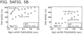
- a maximum TMR ratio of about 200% is obtained. This is a high value that cannot be expected to be realized by an amorphous barrier layer, and shows that the coherent tunneling effect arises markedly due to the crystallization of the Mg-Al-O layer and a high-quality (001) orientation film being achieved. It can be seen that the TMR ratio improves as the MgO insertion layer thickness increases; and finally, there is a trend of saturating.
- FIG. 5B shows the result in the case where MgAl 2 -O x is used.
- a maximum TMR ratio of about 160% is realized.
- MgO insertion of about 0.3 nm which is thicker than that of the Mg 2 Al-O x composition is necessary. It is considered that this is because a stronger template effect was necessary to crystallize the Mg-Al-O layer because a composition having more Al was used.
- FIG. 6A the bias voltage dependence of the TMR ratio normalized with the value of a zero-bias voltage is shown respectively in FIG. 6A for the results of the Mg 2 Al-O x composition and in FIG. 6B for the results of the MgAl 2 -O x composition.
- FIG. 6B the results of the MgAl 2 -O x composition.
- These figures respectively show results for different CoFe insertion layer film thicknesses in which the MgO thickness is fixed at 0.45 nm.
- the direction from the lower layer toward the upper layer was defined as the positive voltage direction in which the electrons tunnel.
- Substantially equivalent behavior can be seen in these figures for each Mg-AI composition.
- the bias voltage dependence of the TMR ratio is small in the positive voltage direction.
- the dependence decreases as the CoFe layer thickness increases.
- the CoFe film thickness dependence is small in the negative voltage direction.
- the positive voltage direction ( V half+ ) has an extremely large value of about 1.4 V when the CoFe layer insertion thickness is 0.92 nm for both Mg-AI compositions. This strongly reflects the state of the upper barrier interface in the positive voltage direction; and it is considered that the high V half+ is caused by the few lattice mismatch defects at the interface where the Mg-Al-O layer and the upper Co-Fe-B layer contact.
- the negative current direction ( V half- ) is about 0.8 V for each condition, and is smaller than that of the positive voltage direction.
- V half- The negative current direction
- the effects of the lattice mismatch remaining at the interface between the CoFe insertion layer and the MgO layer and/or damage due to over-oxidization, etc. are considered.
- FIGS. 8A and 8B An example 4 will now be described using FIGS. 8A and 8B .
- a film of Ta (5 nm)/Ru (10 nm)/Ta (5 nm)/Co 20 Fe 60 B 20 (5 nm)/Co 75 Fe 25 (1.0 nm)/MgO (0.7 nm)/AI-rich composition MgAl 2 -O x (1.2 nm)/Co 20 Fe 60 B 20 (3 nm)/Ta (5 nm)/Ru (5 nm) was formed on a Si substrate having a thermal oxide film; subsequently, heat treatment was performed in a vacuum for 30 minutes at 500 °C.
- the TMR ratio of this multilayer film sample was 220%.
- FIG. 8A A cross-sectional electron microscope image (the STEM image) of the multilayer film is shown in FIG. 8A ; and the results of the composition profile of each element of Mg, Al, O, Fe, and Co using energy dispersive X-ray spectroscopy (EDS) is shown in FIG. 8B .
- EDS energy dispersive X-ray spectroscopy
- the interfaces with the Co-Fe-(B) layers are exceedingly smooth; and because substantially no in-plane lattice mismatch is observed, it can be seen that a high-quality lattice matching interface is realized. Also, it can also be seen that the barrier layer has a composition in which Mg is richer than Al because a relatively thick MgO insertion layer is used.
- a high-quality Mg-Al-O crystal layer can be achieved; and a MTJ element that has both a high TMR ratio and a high can be configured.
- a high performance MTJ element suited to various applications can be provided in which a high element voltage output can be realized.
- FIG. 9 shows the bias voltage dependence of the normalized TMR ratio of the MTJ sample.
- samples using MgO (0.45 nm)/MgAl 2 -O x (1.2 nm) and MgO (0.45 nm)/Mg 2 Al-O x (1.2 nm) also are shown (both using a CoFe insertion layer of 0.9 nm). It can be seen clearly in FIG. 9 that in the positive voltage direction, of the MgO single barrier is small compared to that of the barrier using Mg-AI-O.
- FIG. 10 shows the relationship of the TMR ratio and the RA of the MTJ film sample that was made.
- the TMR ratio was a small value of about 10 to 30% regardless of the magnitude of RA for the samples of each composition. Accordingly, this shows that the coherent tunneling effect does not act effectively in the case where the MgO insertion layer is not used because the crystallization of the Mg-Al-O layer is insufficient.
- the MTJ element of the invention by providing an extremely thin template layer having MgO as a major body in the lower portion of the Mg-Al-O layer, even when amorphous Co-Fe-B is used as the magnetic layer, a conventionally unachievable high TMR ratio can be utilized at room temperature; and it is possible to simultaneously achieve a good bias voltage dependence.
- Being able to use an amorphous magnetic layer with the Mg-Al-O barrier layer means that it is possible to include a barrier layer having good lattice matching in the MTJ element without limiting the types of substrates and/or underlayer structures. Accordingly, utilization is anticipated in various applications utilizing MTJ elements.
- the MTJ element of the invention by using non-deliquescent Mg-Al-O as the barrier layer, it is possible for the damage due to the wet processes used when making fine elements, etc., to be a minimum. Additionally, because a lattice matching barrier interface is obtained, the achievement of a MTJ element having high reliability also can be expected.
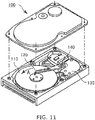
- FIG. 11 is a main component perspective view illustrating a schematic configuration of a magnetic recording and reproducing device in which a magnetic head, in which the MTJ film of the invention is mounted, can be mounted.
- the magnetic recording and reproducing device 100 is a type of device in which a rotary actuator is used.
- a recording medium disk 110 is mounted to a spindle 140 and is rotated in the direction of arrow A by a not-illustrated motor responding to a control signal from a not-illustrated drive device controller.
- the magnetic recording and reproducing device 100 may include multiple medium disks 110.
- a head slider 120 that performs the recording and reproducing of information stored in the medium disk 110 is mounted to the tip of a suspension 152 having a thin-film configuration.
- the head slider 120 has the magnetic head according to the embodiment mounted at the tip vicinity of the head slider 120.
- the medium-opposing surface (the ABS) of the head slider 120 is held at a prescribed fly height from the surface of the medium disk 110.
- the slider may be so-called “contact-sliding" in contact with the medium disk 110.
- the suspension 152 is connected to one end of an actuator arm 154 including a bobbin part (not illustrated) holding a drive coil, etc.
- a voice coil motor 130 which is one type of linear motor is provided at the other end of the actuator arm 154.
- the voice coil motor 130 includes a drive coil (not illustrated) wound onto the bobbin part of the actuator arm 154 and a magnetic circuit (not illustrated) made of a permanent magnet and an opposing yoke arranged to oppose each other with the coil interposed.
- the actuator arm 154 is held by ball bearings (not illustrated) provided in the spindle 140 and can be caused to rotate and slide unrestrictedly by the voice coil motor 130.
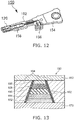
- FIG. 12 is an enlarged perspective view of the magnetic head assembly from the actuator arm 154 tipward viewed from the disk side.
- the magnetic head assembly 150 includes, for example, the actuator arm 154 including the bobbin part holding the drive coil, etc.; and the suspension 152 is connected to one end of the actuator arm 154.
- the head slider 120 that includes the magnetic head shown in FIG. 13 is mounted to the tip of the suspension 152.
- the suspension 152 includes lead wires 158 for writing and reproducing the signals; and the lead wires 158 and electrodes of the magnetic head included in the head slider 120 are electrically connected.
- 156 in the drawing is an electrode pad of the magnetic head assembly 150.
- FIG. 13 is a configuration diagram schematically showing a cross section of the magnetic head reproducing sensor.
- a reproducing sensor 180 is provided between an upper magnetic shield 160 and a lower magnetic shield 170.
- the reproducing sensor 180 is configured by stacking, in order from the lower magnetic shield 170 side toward the upper magnetic shield 160 side, an underlayer layer 182 made of a nonmagnetic conductive layer, a first magnetic layer 184, an intermediate layer 186 (a nonmagnetic insulating layer), a second magnetic layer 188, and a capping layer 190 made of a nonmagnetic conductive layer.
- the reproducing sensor 180 is provided, with an insulating layer 192 interposed, between magnetic domain control films 194 on the left and right that are made of permanent magnet materials.
- the MTJ film first embodiment 101 to the fourth embodiment 401 described above can be utilized in the stacked structure from the underlayer layer 182 to the capping layer 190.
- the underlayer layer 182 corresponds to the underlayer structure layer 22; the first magnetic layer 184 corresponds to the first magnetic layer 1; the intermediate layer 186 corresponds to the stacked film made of the first insulating layer 11 and the second insulating layer 12; the second magnetic layer 188 corresponds to the second magnetic layer 2; and the capping layer 190 corresponds to the upper structure layer 23.
- the layer thickness of the intermediate layer 186 to be from 0.6 to 3 nm including the first insulating layer 11 and the second insulating layer 12. Thereby, it is possible to adjust the exchange coupling between the first magnetic layer 184 and the second magnetic layer 188 and the resistance value of the intermediate layer 186 to optimal values.
- the MTJ element can be utilized in a nonvolatile random access magnetic memory MRAM using the MTJ element as a memory cell.
- the MTJ element of the invention can be utilized in the magnetic head of a magnetic recording and reproducing device, and in a large-capacity magnetic logic circuit. Furthermore, utilization also is possible in a micro-size highly-sensitive sensor and/or spin torque oscillator.
Landscapes
- Engineering & Computer Science (AREA)
- Manufacturing & Machinery (AREA)
- Computer Hardware Design (AREA)
- Hall/Mr Elements (AREA)
- Mram Or Spin Memory Techniques (AREA)
- Thin Magnetic Films (AREA)
- Measuring Magnetic Variables (AREA)
- Magnetic Heads (AREA)
Abstract
Description
- An embodiment of the invention relates to a magnetic tunnel junction, a spintronics device (a magneto-resistance effect element and a magnetic memory device) using the magnetic tunnel junction, and a method for manufacturing a magnetic tunnel junction.
- A magnetic tunnel junction (MTJ) that is made of a three-layer structure of a ferromagnetic layer/insulator layer (barrier layer)/ferromagnetic layer is used as, for example, the magnetic head of a hard disk device or the information recording cell of nonvolatile random access memory (MRAM: Magneto-resistive random access memory). Also, utilization is possible as a compact highly-sensitive magnetic sensor. A MTJ element has a tunnel magneto-resistance effect (TMR: Tunnel magneto-resistance) in which the tunnel resistance value changes via a barrier layer according to the relative magnetization angles of two ferromagnetic layers. In such a field of application, it is desirable to have a high magneto-resistance change ratio (TMR ratio), to be easy to make, and to be makeable on a wide range of substrates.
- A MTJ element that is made of cobalt-iron-boron (CoFeB) as a ferromagnetic layer and magnesium oxide (MgO) as a barrier layer is widely used. The major reason thereof is because CoFeB is amorphous; therefore, there are favorable features for a wide range of element applications such as a high TMR ratio exceeding 100% being obtained relatively easily at room temperature, a MTJ element structure being directly makeable on a wide range of underlayer structures, etc. Especially, the high TMR ratio is caused by the crystallization of the CoFeB layer progressing from the MgO barrier layer. A film of MgO that is formed on the amorphous CoFeB layer by using sputtering, etc., is obtained as a layer having (001) orientation-growth; crystallization of the CoFeB layer progresses from the MgO layer-side interface due to heat treatment at about 200 to 500 °C; and as a result, a high-quality interface crystal structure is realized. Therefore, in the MTJ element that has a CoFeB/MgO/CoFeB structure, a stacked structure in which all three layers have the (001) crystal orientation is realized by the heat treatment; therefore, a large increase of the TMR ratio is observed (Non-Patent Literature 1). The high TMR ratio is due to a coherent tunneling effect via the Δ1-band of the MgO (001).
- On the other hand, because there is lattice mismatch of about 3 to 4% between MgO and CoFeB, there is a problem in which many misfit dislocation defects are introduced at the interface of MgO and CoFeB. Therefore, there is a limit to improving the TMR ratio in a CoFeB/MgO/CoFeB structure. Also, generally, the lattice mismatch is even larger between MgO and the material group other than CoFeB for which there are expectations of utilization as the ferromagnetic layer. For example, because of the large lattice mismatch of 3 to 6% for a Co-based Heusler alloy such as Co2FeAl, Co2MnSi, etc., which are high spin polarization materials and 8 to 10% for FePt, MnGa, etc., which are perpendicular magnetization materials, it is difficult to make a MTJ element having a pronounced coherent tunneling effect by using these ferromagnetic layers with MgO as the barrier layer.
- As a method for making a higher-quality MTJ element by reducing such a large lattice mismatch, there is a method of using MgAl2O4 as the barrier layer (Patent Literature 1). MgAl2O4 has a spinel structure having a lattice constant of about 0.809 nm as a stable structure. The crystal lattice spacing has good lattice matching with a wide range of ferromagnets such as CoFeB, CoFe, Co-based Heusler alloys, FePt, CoPt, MnGa, MnGe, etc., because the crystal lattice spacing is about 4% smaller than MgO which has a rock-salt structure. Also, it is possible to obtain a structure in which the cation sites of a spinel structure are arranged randomly (a cation-disordered spinel structure) as a metastable structure (Patent Literature 2). Furthermore, for MgAl2O4, it is unnecessary for the ratio of Mg and Al to be 1: 2 which is the stoichiometric ratio; the lattice constant can be changed continuously by adjusting the ratio of Mg and Al; therefore, the lattice matching with the ferromagnetic layer can be increased further. Therefore, a more general representation of MgAl2O4 can be written as (Mg1-x Al x )-O x (0 < x < 1). In the case where a MgAl2O4 barrier layer is used as well, the coherent effect arises; and a large TMR ratio exceeding 300% at room temperature is realized (Patent Literature 2). Also, a problem is known in which the TMR ratio decreases due to the application of a bias voltage in a MTJ element; and this is a practical problem (bias voltage dependence). It is also known that the degree of the decrease of the TMR ratio can be reduced if the lattice mismatch is reduced by introducing the MgAl2O4 barrier layer (Patent Literature 1). Furthermore, it is known that a strong perpendicular magnetic anisotropy can be introduced to an extremely thin ferromagnetic layer contacting MgAl2O; and due to this effect, a perpendicular magnetization MTJ element that is suited to increasing the capacity of MRAM can be configured (Patent Literature 3).
- However, it is necessary to obtain a crystalline MgAl2O4 barrier layer to make a high performance MTJ element having a high room temperature TMR ratio, good bias voltage characteristics, etc.; and to this end, an underlayer structure of a single-crystal ferromagnetic layer, e.g., Fe, CoFe alloys, or a Co2FeAl alloy was necessary. Therefore, there were problems in applications such as the utilizable substrates and underlayer materials being extremely limited. Especially, there was a problem in which an amorphous MgAl2O4 layer is obtained if the MgAl2O4 layer is formed on amorphous CoFeB; therefore, the crystallization of the MTJ element cannot be realized; therefore, the coherent tunneling effect is not obtained; and a high TMR ratio such as a TMR ratio exceeding 100% cannot be realized using the CoFeB layer and the MgAl2O4 barrier layer (
Non-Patent Literature 2 and Non-Patent Literature 3). -
- Patent Literature 1: Japanese Patent No.
5586028 - Patent Literature 2: Japanese Patent No.
5988019 - Patent Literature 3:
JP-A 2017-041606 -
- Non-Patent Literature 1: D. D. Djayaprawira, K. Tsunekawa, M. Nagai, H. Maehara, S. Yamagata, N. Watanabe, S. Yuasa, Y. Suzuki, and K. Ando, Appl. Phys. Lett., Vol. 86, p. 092502 (2005).
- Non-Patent Literature 2: M. Tsunoda, R. Chiba, and K. Kabara, J. Appl. Phys., Vol. 117, p. 17D703 (2015).
- Non-Patent Literature 3: H. Liu, Q. Ma, S. Rizwan, D. Liu, S. Wang, and X. Han, IEEE Trans. Magn., Vol. 47, p. 2716 (2011).
- Considering such an actual situation, the invention is directed to achieve a high TMR ratio by realizing a MTJ element including a CoFeB layer and a MgAl2O4 barrier layer without using a conventional single-crystal underlayer. It is also directed to suppress the bias voltage dependence of the TMR ratio.
- In the process of research relating to a MTJ element using MgAl2O4 as a barrier layer, the inventors discovered that by forming a MgAl2O4 film after forming extremely thin MgO on a CoFeB layer, crystallization of the MgAl2O4 layer occurs; and a MgO/MgAl2O4 stacked film is obtained as an oriented film having (001) growth. As a result, the inventors discovered that all of the layers of the stacked film made of the CoFeB/MgO/MgAl2O4/CoFeB structure are crystallized by heat treatment so that the stacked film functions as a MTJ element realizing a high TMR ratio. Simultaneously, the discovery that the bias voltage dependence is improved by the effect of the MgO/MgAl2O4 stacked barrier layer having a small lattice mismatch with CoFeB also led to the invention.
- [1] A magnetic tunnel junction including a tunnel barrier layer provided between a first magnetic layer and a second magnetic layer, the tunnel barrier layer being a crystal body made of a stacked structure of a first insulating layer and a second insulating layer, the crystal body being oriented, the first insulating layer being made of an oxide of Mg1-x X x (0 ≤ x ≤ 0.15), X including at least one element selected from the group consisting of Al and Ti, the second insulating layer being made of an oxide of an alloy including at least two elements selected from the group consisting of Mg, Al, Zn, and Li, both the first magnetic layer and the second magnetic layer being made of an alloy including B and at least one element selected from the group consisting of Co and Fe.
- [2] The magnetic tunnel junction according to [1], wherein a layer including at least one element selected from the group consisting of Co and Fe is further provided at both or one of between the tunnel barrier layer and the first magnetic layer or between the tunnel barrier layer and the second magnetic layer.
- [3] The magnetic tunnel junction according to [1] or [2], wherein the first insulating layer is made of MgO.
- [4] The tunnel junction according to any one of [1] to [3], wherein the second insulating layer is made of an oxide of Mg1-y Al y (0.2 ≤ y ≤ 0.8).
- [5] The magnetic tunnel junction according to any one of [1] to [4], having a tunnel magneto-resistance not less than 120% and not more than 34000% at room temperature.
- [6] A spintronics device, comprising the magnetic tunnel junction according to any one of [1] to [5].
- [7] The spintronics device according to [6], wherein the spintronics device is one of a hard disk magnetic head, a spin torque rewritable MRAM (a STT-MRAM), a three-terminal MRAM, a voltage-driven MRAM, a spin torque oscillator, or a spin resonance tunnel element.
- [8] A method for manufacturing a magnetic tunnel junction, comprising: a process of introducing a substrate (e.g., Si) to a sputtering apparatus; a process of forming a first magnetic layer (e.g., a Co-Fe-B layer); a process of forming a first insulating layer (e.g., a MgO film) to overlap the first magnetic layer; a process of forming a second insulating layer (e.g., a Mg-Al-O layer) to overlap the first insulating layer; a process of forming a second magnetic layer (e.g., a Co20Fe60B20 layer) to overlap the second insulating layer; and a process of performing heat treatment of a multilayer film structure that is made, the heat treatment being performed in a vacuum for 1 minute to 60 minutes at a temperature range from 300 °C to 500 °C.
- [9] The method for manufacturing the magnetic tunnel junction according to [8], wherein the first magnetic layer formation process is performed after forming an underlayer structure film (e.g., Ta) at the substrate.
- [10] The method for manufacturing the magnetic tunnel junction according to [8] or [9], wherein a process of forming a second magnetic insertion layer (e.g., a CoFe film) to overlap the first magnetic layer is performed between the first magnetic layer formation process and the first insulating layer formation process.
- [11] The method for manufacturing the magnetic tunnel junction according to any one of [8] to [10], wherein a process of forming a second magnetic insertion layer (e.g., a CoFe film) to overlap the second insulating layer is performed between the second insulating layer formation process and the second magnetic layer formation process.
- [12] The method for manufacturing the magnetic tunnel junction according to any one of [8] to [11], wherein a process of forming an upper structure film (e.g., Ta) to overlap the second magnetic layer is performed between the second magnetic layer formation process and the heat treatment process.
- In the invention, a barrier layer that is made of Mg-Al-O having a small lattice mismatch with CoFeB is provided; and as a result, for example, a MTJ element in which a large TMR ratio is obtained and a method for making the MTJ element are provided. Here, a large TMR ratio is the obtainment of a TMR ratio of 120% or more at room temperature. Also, the bias voltage dependence of the TMR ratio can be improved; and when a bias voltage Vhalf at which the TMR ratio is halved is used as an indicator of the bias voltage dependence, a value exceeding Vhalf = 1 V can be realized. Therefore, it is possible to improve the electrical output of the MTJ element. The MTJ element of the invention not only is applicable to a hard disk magnetic head and a spin torque rewritable MRAM (a STT-MRAM), but also can be utilized in many spintronics devices such as a three-terminal MRAM, a voltage-driven MRAM, a spin torque oscillator, a spin resonance tunnel element, etc.
-
- [
FIG. 1 ]
FIGS. 1A and B are schematic cross-sectional views of a magnetic tunnel junction (MTJ) element film according to one embodiment of the invention. - [
FIG. 2 ]
FIGS. 2A and B are schematic cross-sectional views of other examples of MTJ element films according to one embodiment of the invention. - [
FIG. 3 ]
FIG. 3 shows X-ray diffraction patterns when the CoFe layer thickness is changed in a multilayer film structure of Ta/Co-Fe-B/CoFe/MgO (0.25 nm)/Mg2Al-O x (10 nm)/Co-Fe-B/Ta. (A) is the film in-plane direction scan result; and (B) is the film out-of-plane direction scan result. - [
FIG. 4 ]
FIG. 4 is a figure showing the relationship of a CoFe insertion layer thickness with (A) the crystal lattice spacing and (B) the crystal lattice volume determined from X-ray diffraction patterns for each of Mg2Al-O x and MgAl2-O x as the Mg-Al-O layer in a multilayer film structure of Ta/Co-Fe-B/CoFe/MgO (0.25 nm)/Mg-Al-O (10 nm)/Co-Fe-B/Ta. - [
FIG. 5 ]
FIG. 5 shows the relationship between the MgO layer thickness and the TMR ratio of a MTJ element made with a CoFe film thickness of 0.16 nm and 0.92 nm. (A) is the result using Mg2Al-O x ; and (B) is the result using MgAl2-O x . - [
FIG. 6 ]
FIG. 6 is a figure showing the bias voltage dependence of the TMR ratio normalized using the value of zero voltage. (A) is the result using Mg2Al-O x ; and (B) is the result using MgAl2-O x . - [
FIG. 7 ]
FIG. 7 is a figure of the measurement of the external magnetic field dependence of the TMR ratio and the electrical resistance of a MTJ element using Mg2Al-O x on which heat treatment is performed at 500 °C. - [
FIG. 8 ]
FIG. 8A shows a cross-sectional electron microscope image (a STEM image) of an element having a MgO (0.7 nm)/MgAl2-O x (1.2 nm) stacked barrier layer on which heat treatment is performed at 500 °C.FIG. 8B shows the elemental analysis results using energy dispersive X-ray spectroscopy (EDS). - [
FIG. 9 ]
FIG. 9 is a figure showing the bias voltage dependence for a MTJ element having a MgO single barrier layer and a MTJ element having a MgO/Mg-Al-O stacked barrier layer. - [
FIG. 10 ]
FIG. 10 is a figure showing the relationship of the TMR ratio and the resistance area (RA) of a MTJ film having a Co-Fe-B/Mg-AI-O/Co-Fe-B structure (after heat treatment at 300 °C). - [
FIG. 11 ]
FIG. 11 is a schematic view showing an example of a magnetic recording and reproducing device in which the MTJ element of the invention is mounted. - [
FIG. 12 ]
FIG. 12 is a schematic view showing an example of a magnetic head assembly in which the MTJ element of the invention is mounted. - [
FIG. 13 ]
FIG. 13 is a configuration diagram schematically showing the cross section of a magnetic head reproducing sensor in which the MTJ element of the invention is mounted. - The tunnel barrier of the embodiment and embodiments of MTJ elements using the tunnel barrier will now be described with reference to
FIG. 1A, FIG. 1B, FIG. 2A, and FIG. 2B . - The MTJ element of the embodiment is an element in which a first magnetic layer, a first insulating layer, a second insulating layer, and a second magnetic layer are stacked in this order on a substrate. The first insulating layer and the second insulating layer are made of oxides. As an example, the first magnetic layer and the second magnetic layer are made of CoFeB; and the first insulating layer and the second insulating layer respectively have MgO and MgAl2O4 as major bodies.
- In such a case, it is unnecessary for the Mg: Al ratio of MgAl2O4 to be 1: 2 in the second insulating layer; and compositions having a wide range of ratios can be used (hereinafter, recited using the general notation of Mg-AI-O). Also, both a spinel structure and a cation-disordered spinel structure can be used as the crystal structure of Mg-AI-O. Also, other than Mg and Al, the elements that form the spinel structure may include, for example, an oxide including Li and Zn. Also, other than MgO, the first insulating layer may have a stacked structure of a metal Mg layer/MgO layer or a structure including a small amount of Al or Ti. Also, the effects also are realized in a structure in which a CoFe alloy is inserted between the first magnetic layer and the first insulating layer and/or between the second magnetic layer and the second insulating layer.
- A MTJ film
first embodiment 101 which is the basic structure of a first embodiment is shown inFIG. 1A . The MTJ filmfirst embodiment 101 has a multilayer film structure; and a firstmagnetic layer 1, a first insulatinglayer 11, a second insulatinglayer 12, and a secondmagnetic layer 2 are stacked in order from the bottom. Either of the firstmagnetic layer 1 and the secondmagnetic layer 2 may be a fixed magnetic layer or a free magnetic layer. Also, the magnetization direction may be either a film in-plane direction or a film out-of-plane direction. The fabrication method and the effects of the structure of the MTJ filmfirst embodiment 101 will now be described. - The first
magnetic layer 1 is, for example, a layer made of Co-Fe-B formed by physical vapor deposition such as sputtering, vapor deposition, etc. The Co-Fe-B has an amorphous structure at this stage. It is sufficient for the composition of Co and Fe to be Co1-n Fe n (0 ≤ n ≤ 1); and the composition of Co and Fe is a composition that includes CoB and FeB. It is sufficient for the B composition inside Co-Fe-B to be in a range in which the Co-Fe-B layer is ferromagnetic and amorphous; and the B composition in Co-Fe-B is, for example, about 15 to 25 atomic%. The thickness of this layer is, for example, 0.8 to 5 nm but is determined to be in balance with the lower layer structure of the firstmagnetic layer 1. Also, this layer also can be obtained as a layer having perpendicular magnetization by setting this layer to be extremely thin with a thickness of not more than about 1.5 nm. - Then, the first insulating
layer 11 is a layer made of an oxide having MgO as a major body. The oxygen amount may be somewhat deficient or excessive; and effects are obtained in the range of MgO1+δ (-0.2 ≤ δ ≤ 0.2). This layer can be utilized because this layer is obtained as a crystal layer even if Al or Ti is included at about 15 atomic% with respect to Mg. Also, the first insulatinglayer 11 has the effect of promoting the crystallization of the second insulatinglayer 12 formed on the first insulatinglayer 11 and is a crystal film having substantially (001) growth, but may partially include amorphous and/or polycrystalline bodies at this stage. To control the crystal structure of the first insulatinglayer 11, for example, heat treatment in a vacuum at a range of about 100 to 400 °C also can be performed after the formation of this layer. - Then, the second insulating
layer 12 is formed on the first insulatinglayer 11. The second insulatinglayer 12 is a hybrid oxide layer having Mg-Al-O as a major component. This layer can have a cubic crystal body. Also, the composition is such that a spinel structure is the stable structure. Mg1-y Al y (0.2 ≤ y ≤ 0.8) can be used as the composition of Mg and Al. Here, y is set to be 0.2 or more to obtain the effect of improving V half, because the lattice mismatch between the firstmagnetic body 1 and the secondmagnetic body 2 can be reduced to be about 3% or less. Also, y is set to be 0.8 or less because the crystallization of Mg-Al-O becomes difficult due to the effect of the Al-rich composition. Also, the effects are obtained even if the oxygen amount of this layer is deficient or excessive with respect to the stoichiometric composition; for example, as a general formula, a range of Mg1-x Al x O1.5-x/2+δ' (-0.2 ≤ δ' ≤ 0.2) can be utilized. Also, a portion of Mg and Al may be replaced with Zn and Li with the object of stabilizing the spinel structure, adjusting the insulative characteristics and the element resistance, and/or improving the TMR ratio. This is because the Al oxides of ZnAl2O4 and LiAl2.5O4 that include Zn and Li are insulating bodies having spinel structure crystals having about the same lattice constant as MgAl2O4. The effects of the embodiment are realized even if Zn and Li are included because a solid solution that is continuous with MgAl2O4 can be made due to the feature of these material properties being similar. Also, to control the crystal structure of the second insulatinglayer 12, for example, heat treatment in a vacuum at the range of 100 to 400 °C also can be performed after the formation of this layer. - Various known methods can be used to make the first insulating
layer 11 and the second insulatinglayer 12. For example, high frequency sputtering from a target material made of an oxide, reactive vapor deposition or reactive sputtering using an oxygen gas, a method of oxidizing after forming a metal layer made of an alloy of Mg or Mg1-a Al a (0 < a ≤ 1) (post oxidation), multistep post oxidation, or a technique in which these techniques are combined can be used. These techniques may be performed while heating the substrate at a temperature in a range that does not degrade the flatness. - For example, the range of 0.05 to 1.2 nm is favorable as the thickness of the first insulating
layer 11. 0.1 to 1.0 nm is more favorable. 0.2 to 0.8 nm is more favorable. 0.05 nm corresponds to the thickness of about 1/4 of one atomic plane of MgO (001); and this thickness or more can function as a crystal template for obtaining the second insulatinglayer 12 as a crystal layer. As the first insulatinglayer 11 film thickness increases, the crystal template effect improves; and the crystallization of the second insulatinglayer 12 can be realized at a lower heat treatment temperature. On the other hand, because there is lattice mismatch of about 4% between MgO and Co-Fe-B, thoughtlessly increasing the first insulatinglayer 11 film thickness causes the effects of the lattice mismatch between the firstmagnetic layer 1 and the first insulatinglayer 11 to increase; therefore, there is a risk that V half may decrease. - Although the thickness is not limited in terms of crystallizing the second insulating
layer 12, to provide a practical resistance area (resistance R × area A; the RA value) as the MTJ element, it is favorable for the thickness to be 3 nm or less; and it is more favorable for the thickness to be 2 nm or less. To effectively reduce the lattice mismatch between the firstmagnetic layer 1 and the stacked insulating layer and between the secondmagnetic layer 2 and the stacked insulating layer and to obtain a high V half, it is favorable for the second insulatinglayer 12 film thickness to be equal to or greater than the first insulatinglayer 11 layer thickness. Taking into account the description recited above, for the object of the MTJ element, it is favorable for the total thickness of the stacked film of the first insulating layer and the second insulating layer to be 0.6 nm to 3 nm. - Also, the control of the interface crystal structure and/or the adjustment of the perpendicular magnetic anisotropy also can be performed by inserting an extremely thin metal film made of Mg1-b Al b (0 ≤ b ≤ 1) and having a thickness of, for example, 1 nm or less between the first
magnetic layer 1 and the first insulatinglayer 11 and/or between the second insulatinglayer 12 and the secondmagnetic layer 2. - Then, the second
magnetic layer 2 is formed on the second insulatinglayer 12. Similarly to the firstmagnetic layer 1, the secondmagnetic layer 2 also is a layer having an amorphous structure and having Co-Fe-B as a major body. The same technique as the firstmagnetic layer 1 can be used as the method for making the layer. - After forming the multilayer film structure recited above, for example, by performing heat treatment in a vacuum for 1 minute to 60 minutes at a temperature range of about 200 to 500 °C, the structure changes to a cubic structure as an entirety; and a crystal multilayer film that has substantially the (001) orientation is formed. By adjusting the heat treatment conditions, mutual atomic diffusion can be promoted partially or as an entirety in the first insulating
layer 11 and the second insulatinglayer 12; and one body of a Mg-Al-O barrier layer also can be obtained. Due to this effect, it is possible to obtain a Co-Fe-B/Mg-AI-O/Co-Fe-B stacked structure having good lattice matching; and a higher V half can be obtained while realizing a high TMR ratio equal to that of a known single-layer MgO barrier element. For example, according to the invention, a magnetic tunnel junction that has a tunnel magneto-resistance not less than 120% and not more than 34000% at room temperature is made. - A second embodiment is shown as a MTJ film
second embodiment 201 inFIG. 1B and will now be described. The MTJ filmsecond embodiment 201 is the MTJ filmfirst embodiment 101 in which amagnetic insertion layer 3 is newly provided between the firstmagnetic layer 1 and the first insulatinglayer 11. Otherwise, a structure, a composition, and a manufacturing method equivalent to those of the MTJ filmfirst embodiment 101 can be used. Themagnetic insertion layer 3 is a thin insertion layer made of Co1-m Fe m (0 < m ≤ 1). Themagnetic insertion layer 3 has the effect of promoting the crystallization of both the first insulatinglayer 11 and the second insulatinglayer 12, and causes the improvement of the TMR ratio. It is favorable for the film thickness of this layer to be thinner than the firstmagnetic layer 1, e.g., 0.1 to 1.5 nm. Themagnetic insertion layer 3 can be made using the same technique as Co-Fe-B such as sputtering, vacuum vapor deposition, etc. To improve the flatness of themagnetic insertion layer 3, heat treatment may be performed in a vacuum at a temperature of 100 to 300 °C. Also, a CoFe alloy layer may be inserted using a technique similar to that of themagnetic insertion layer 3 also between the second insulatinglayer 12 and the secondmagnetic layer 2. - As shown typically as a MTJ film
third embodiment 301 inFIG. 2A , a third embodiment is the MTJ filmfirst embodiment 101 in which a lower structure of the firstmagnetic layer 1 and an upper structure of the secondmagnetic layer 2 are newly provided. First, asubstrate 21 is provided; and anunderlayer structure layer 22 is provided on thesubstrate 21. The MTJ filmfirst embodiment 101 is provided on theunderlayer structure layer 22. Also, anupper structure layer 23 is provided on the MTJ filmfirst embodiment 101. - It is desirable for the
substrate 21 to be flat and homogeneous. As the material, for example, a Si-based material such as Si, Si having a thermal oxide film (Si/SiO2), SiN, SiC, etc., a compound semiconductor such as GaAs, etc., or an oxide crystal such as MgO, MgAl2O4, sapphire, etc., can be used. - The
underlayer structure layer 22 is provided between thesubstrate 21 and the firstmagnetic layer 1, is used as an electrode layer on the lower side, and is used for controlling the magnetic properties and/or the crystal structure of the first magnetic layer. A known multilayer structure can be utilized in theunderlayer structure layer 22. For example, as the electrode layer, a layer that includes at least one selected from the group consisting of Ta, TaN, Ru, Ir, Pt, W, Ti, TiN, AITiC, Cu, CuN, Mo, Cr, Au, Ag, NiAl, NiFe, IrMn, and PtMn can be used. Also, an oxide layer of MgO, MgAl2O4, AlOx, SiOx, SrTiO3, etc., may be included between the electrode layer and thesubstrate 21. These oxide layers can be used for controlling the crystal orientation of the electrode layer. - A magnetic layer may be included between the electrode layer and the first
magnetic layer 1; for example, Co-Fe alloys, Co-Fe-Tb alloys, Mn-Ga alloys, Mn-Ge alloys, Mn-Ga-N, Fe-Pt alloys, Co-Pt alloys, etc., or a stacked film of these alloys may be used. Also, Co-based Heusler alloys that are represented by Co2YZ (Y being Fe, Mn, Ti, V, Cr, etc., and Z being Al, Si, Sn, Ga, Ge, etc.) also can be used. Also, the structure may be a multilayer stack of a layer including at least one element selected from (Co or Fe) and a layer including at least one element selected from (Pt or Pd). A nonmagnetic layer of Ru, Ti, W, Mo, Ir, etc., may be inserted between the layers including these magnetic bodies. Heat treatment in a vacuum also can be performed for each of these layers. - Examples of the stacking of the
underlayer structure layer 22 are, from the bottom, a Ta (5 nm)/Ru (10 nm)/NiFe (5 nm)/IrMn (10 nm)/CoFe (2.5 nm)/Ru (0.8 nm)/CoFe (2 nm) structure, a Ta (5 nm)/Ru (10 nm)/Pt (3 nm)/[Co (0.2 nm)/Pt (0.4 nm)] multilayer film/Co (0.2 nm)/Ru (0.8 nm)/[Co (0.2 nm)/Pt (0.4 nm)] multilayer film/CoFeB (1 nm)/Ta (0.2 nm) structure, and a MgO (7 nm)/Cr (40 nm)/Co2FeAl (5 nm) structure. Here, the film thickness is inside (). - The
upper structure film 23 is provided on the secondmagnetic layer 2. For example, theupper structure film 23 functions as an upper electrode and as a protective film of the magnetic tunnel junction film as well. For example, Ta (5 nm)/Ru (15 nm) can be used. Ta has the property of absorbing a portion of the B of Co-Fe-B during the heat treatment, and as a result of being provided directly on the Co-Fe-B, also has the effect of promoting the crystallization of the Co-Fe-B layer. Furthermore, the structure of theunderlayer structure layer 22 that includes the magnetic body may be included to control the magnetic properties and/or the crystal structure of the secondmagnetic layer 2. For example, the structure is a Ta/CoFe/Ta/Ru structure or a W/[Co/Pd] multilayer film/Ta/Ru structure from the bottom. Furthermore, a thin oxide layer such as MgO, etc., may be included, e.g., a Ta/Co-Fe-B/MgO/Ta/Ru structure. - As shown typically as a MTJ film
fourth embodiment 401 inFIG. 2B , a fourth embodiment is the MTJ filmthird embodiment 301 in which themagnetic insertion layer 3 is newly provided between the firstmagnetic layer 1 and the first insulatinglayer 11. As shown in the MTJ filmsecond embodiment 201, the layer is a layer made of CoFe alloys and has the effect of promoting the crystallization of the first insulatinglayer 11 and the second insulatinglayer 12. - The descriptions recited above are descriptions of typical examples of embodiments of the invention and are not limited to the designated embodiments; and modifications within the spirit described in the Claims of course are possible.
- The tunnel barrier of the embodiment and examples of MTJ elements using the tunnel barrier of the embodiment will now be described with reference to
FIG. 3 to FIG. 8 . - An example 1 will now be described using
FIG. 3A, FIG. 3B ,FIG. 4A, and FIG. 4B . A Si substrate having a thermal oxide film is used as a substrate, and is introduced to a sputtering apparatus after cleaning using isopropyl alcohol. A film of Ta (5 nm)/Co-Fe-B (5 nm) is formed at room temperature using magnetron sputtering. The Ta is an underlayer structure film; and the Co-Fe-B layer is the first magnetic layer. The composition of the target used in the formation of the Co-Fe-B layer is Co20Fe60B20. Then, sputtering film formation of CoFe films of 0 (no insertion layer), 0.3, 0.6, and 0.9 nm was performed as a magnetic insertion layer. The target that was used has a Co75Fe25 composition. Then, a film of MgO (0.25 nm) was formed as the first insulating layer by high frequency sputtering using a MgO sintering target. Continuing, a Mg-Al-O layer (10 nm) was formed by high frequency sputtering using a target having two different compositions. - For the first composition, a Mg-rich (Mg0.67Al0.33)-O x target was used; and the actual composition of Mg and Al of the Mg-Al-O layer was Mg0.72Al0.28 by using inductively coupled plasma composition analysis. Hereinafter, this composition is called Mg2Al-O x for convenience.
- For the second composition, an Al-rich (Mg0.33Al0.67)-O x target was used; and the actual composition of Mg and Al was Mg0.39Al0.61. Hereinafter, this composition is called MgAl2-O x for convenience. Then, a film of Co20Fe60B20 (5 nm) was formed as the second magnetic layer on the Mg-Al-O layer; and a film of Ta (5 nm) was formed as an upper structure film on the second magnetic layer. Subsequently, heat treatment of the multilayer film structure that was made was performed in a vacuum for 30 minutes at 300 °C.
-
FIG. 3A shows X-ray diffraction patterns obtained by scanning, in the film out-of-plane direction, the multilayer film structure in the case where the Mg-rich Mg2Al-O x is used. The patterns are shown separately for each CoFe insertion layer thickness. For each of the CoFe film thicknesses, a peak that corresponds to MgAl2O4 (004) is observed at the 42° vicinity. Other than this peak, it can be seen that there are only the peaks other than the substrate and the Ta layer. This shows that the Mg2Al-O x layer is crystallized; and (001) growth is realized. It can be seen that the MgAl2O4 (004) peak intensity increases as the CoFe insertion thickness increases. Accordingly, this shows that the insertion of the CoFe layer promotes the crystallization of MgAl2O4. - Similarly,
FIG. 3B shows X-ray diffraction patterns obtained by scanning, in the film in-plane direction, the multilayer film structure of each CoFe insertion layer thickness. A peak that has MgAl2O4 (400) and CoFe (110) as the origin is observed. The intensity of this peak also increases as the CoFe insertion layer thickness increases; therefore, it can be confirmed that there is a crystallization promotion effect of MgAl2O4 due to the CoFe layer insertion. In all of the samples for which X-ray diffraction patterns were measured, an ordered spinel structure of the Mg-Al-O layer was not observed. Therefore, it can be said that the structure is a cation-disordered spinel structure having a lattice constant that is half of the original lattice constant of MgAl2O4. - The crystallization of a similar Mg-Al-O layer was confirmed from the X-ray diffraction pattern for the MgAl2-O x composition as well. The crystal lattice spacing in the film surface and in the film out-of-plane direction of the formed Mg-Al-O was estimated from the observed X-ray peak positions, the MgAl2O4 (004) and (400).
-
FIG. 4A shows the relationship of the crystal lattice spacing with the CoFe insertion layer thickness for each of Mg2Al-O x and MgAl2-O x . From this figure, it can be seen that the lattice spacing substantially does not affect the CoFe film thickness for each of the compositions. Also, it can be seen that the lattice spacing in the film in-plane direction is smaller than the spacing in the film out-of-plane direction. The in-plane lattice spacing is in the range of 0.405 to 0.408 nm for each of the compositions. These values are near the MgAl2O4 bulk value (0.4045 nm) and suggest that the crystal extends in the film out-of-plane direction (tetragonal distortion is introduced) so that good in-plane lattice matching with the Co-Fe-B layer is realized. Furthermore, it can be seen that the lattice constant in the film out-of-plane direction is different according to the Mg-AI composition. - The crystal lattice volume is calculated in
FIG. 4B . MgAl2-O x has a value near the bulk value (1/8 unit cell) of MgAl2O4 converted to a value when the lattice constant is considered to be half. On the other hand, it can be seen that Mg2Al-O x has a value near the average value of the MgO bulk value and the MgAl2O4 bulk converted value. Accordingly, this also suggests that continuous control of the crystal lattice volume is possible by adjusting the Mg-AI composition. It can also be seen that even for the Mg-rich composition which originally has lattice mismatch, in-plane lattice matching is realized by easily introducing tetragonal distortion. Thus, it was confirmed that the Mg-Al-O layer is crystallized by inserting extremely thin MgO between the Mg-Al-O layer and the Co-Fe-B layer; and the crystallinity is improved further by the CoFe layer insertion. Also, it was also found that an in-plane lattice matching state with the Co-Fe-B layer can be realized for a wide range of compositions of Mg-AI. - An example 2 will now be described using
FIG. 5A, FIG. 5B ,FIG. 6A, and FIG. 6 . Using a method equivalent to that of the example 1, an underlayer structure film of Ta (5 nm)/Ru (10 nm)/Ta (5 nm) was made on a Si substrate having a thermal oxide film. Then, after forming the first magnetic layer of Co20Fe60B20 (5 nm), sputtering film formation of a Co75Fe25 film was performed as a magnetic insertion layer. The film thickness of the Co75Fe25 layer was changed in the range of 0.1 to 1.0 nm. Then, a MgO layer was formed as the first insulating layer by changing the film thickness to be 0.1 to 0.8 nm. Continuing, high frequency sputtering film formation of Mg2Al-O x or MgAl2-O x having a thickness of 1.2 nm was performed as the second insulating layer. Subsequently, a film of Co20Fe60B20 (3 nm)/Ta (5 nm)/Ru (5 nm) was formed. After making the multilayer film, the MTJ element structure was formed by performing fine patterning into an elliptical shape having a size of 400 nm×200 nm by using electron beam lithography, photolithography, and an ion etching apparatus. Also, Au was used as a measurement electrode. Subsequently, heat treatment of the MTJ element was performed in a vacuum for 30 minutes at 400 °C. Then, the change of the electrical resistance of the MTJ element was measured at room temperature for an external magnetic field and a bias voltage by a DC four-terminal technique. The TMR ratio (%) was defined as 100×(R AP-R P)/R P, wherein the resistance value when the magnetic ordering of the magnetic layers above and below is antiparallel is R AP, and the resistance value when the magnetic ordering of the magnetic layers above and below is parallel is R P. -
FIG. 5A shows the relationship between the TMR ratio and the MgO layer thickness in the case where Mg2Al-O x is used and the CoFe film thickness = 0.16 nm and 0.92 nm is fixed. In the example, a maximum TMR ratio of about 200% is obtained. This is a high value that cannot be expected to be realized by an amorphous barrier layer, and shows that the coherent tunneling effect arises markedly due to the crystallization of the Mg-Al-O layer and a high-quality (001) orientation film being achieved. It can be seen that the TMR ratio improves as the MgO insertion layer thickness increases; and finally, there is a trend of saturating. In particular, in the case where a thick CoFe layer thickness of 0.92 nm is used, a sufficient effect is realized if MgO is about 0.15 nm. Also, even in a thin MgO region of 0.05 nm, a relatively high value of about 130% is realized. On the other hand, in the case of a thin CoFe layer of 0.16 nm, it can be seen that the TMR ratio is low as an entirety; and a relatively thick MgO layer insertion is necessary to obtain a high TMR ratio. Accordingly, it can be seen that the CoFe insertion layer thickness also greatly affects the crystallization of the Mg-Al-O layer. -
FIG. 5B shows the result in the case where MgAl2-O x is used. A maximum TMR ratio of about 160% is realized. However, to obtain a TMR ratio exceeding 100%, MgO insertion of about 0.3 nm which is thicker than that of the Mg2Al-O x composition is necessary. It is considered that this is because a stronger template effect was necessary to crystallize the Mg-Al-O layer because a composition having more Al was used. - Then, the bias voltage dependence of the TMR ratio normalized with the value of a zero-bias voltage is shown respectively in
FIG. 6A for the results of the Mg2Al-O x composition and inFIG. 6B for the results of the MgAl2-O x composition. These figures respectively show results for different CoFe insertion layer film thicknesses in which the MgO thickness is fixed at 0.45 nm. Also, the direction from the lower layer toward the upper layer was defined as the positive voltage direction in which the electrons tunnel. Substantially equivalent behavior can be seen in these figures for each Mg-AI composition. In other words, it can be seen that the bias voltage dependence of the TMR ratio is small in the positive voltage direction. In particular, the dependence decreases as the CoFe layer thickness increases. On the other hand, the CoFe film thickness dependence is small in the negative voltage direction. - The bias voltage at which the normalized TMR = 0.5 means and is a simple indicator of the bias voltage dependence. The positive voltage direction (V half+) has an extremely large value of about 1.4 V when the CoFe layer insertion thickness is 0.92 nm for both Mg-AI compositions. This strongly reflects the state of the upper barrier interface in the positive voltage direction; and it is considered that the high V half+ is caused by the few lattice mismatch defects at the interface where the Mg-Al-O layer and the upper Co-Fe-B layer contact.
- The negative current direction (V half-) is about 0.8 V for each condition, and is smaller than that of the positive voltage direction. As possibilities thereof, the effects of the lattice mismatch remaining at the interface between the CoFe insertion layer and the MgO layer and/or damage due to over-oxidization, etc., are considered. Also, generally, is greatly affected by the magnetic layer composition, and when Co-Fe-(B)-based, decreases as the Co composition increases. Accordingly, it can be said that the Co-rich composition of Co75Fe25 used in the insertion layer also causes V half- to decrease.
- An example 3 will now be described using
FIG. 7 . Using a method equivalent to that of the example 2, a film of Ta (5 nm)/Ru (10 nm)/Ta (5 nm)/Co20Fe60B20 (5 nm)/Co75Fe25 (1.0 nm)/MgO (0.4 nm)/Mg-rich composition Mg2Al-O x (1.2 nm)/Co20Fe60B20 (3 nm)/Ta (5 nm)/Ru (5 nm) was formed on a Si substrate having a thermal oxide film; and fine patterning was performed. Subsequently, heat treatment was performed in a vacuum for 30 minutes at 500 °C. The measurement results of the external magnetic field dependence of the element resistance and the TMR ratio are shown inFIG. 7 . It can be seen from the figure that the TMR ratio = 242% was obtained; and this value that was obtained is a value that is higher than the maximum value (about 200%) for heat treatment at 400 °C. This is because the crystallization of each layer progressed effectively by performing the heat treatment at a higher temperature. - An example 4 will now be described using
FIGS. 8A and 8B . Using a method equivalent to that of the examples 2 and 3, a film of Ta (5 nm)/Ru (10 nm)/Ta (5 nm)/Co20Fe60B20 (5 nm)/Co75Fe25 (1.0 nm)/MgO (0.7 nm)/AI-rich composition MgAl2-O x (1.2 nm)/Co20Fe60B20 (3 nm)/Ta (5 nm)/Ru (5 nm) was formed on a Si substrate having a thermal oxide film; subsequently, heat treatment was performed in a vacuum for 30 minutes at 500 °C. The TMR ratio of this multilayer film sample was 220%. A cross-sectional electron microscope image (the STEM image) of the multilayer film is shown inFIG. 8A ; and the results of the composition profile of each element of Mg, Al, O, Fe, and Co using energy dispersive X-ray spectroscopy (EDS) is shown inFIG. 8B . - From the cross-sectional STEM image, it can be seen that the upper and lower magnetic layers and the stacked barrier layer are crystallized. Also, it was found that all of these layers have (001) growth. Also, it can also be seen that no distinct boundary inside the MgO/MgAl2-O x stacked barrier layer is observed; and the appearance is that of one body. From the EDS element profile as well, Mg and Al have mutual diffusion inside the MgO/MgAl2-O x stacked barrier layer and have a substantially uniform Mg-AI concentration; and a crystallized Mg-Al-O barrier is realized between the upper and lower magnetic layers. The interfaces with the Co-Fe-(B) layers are exceedingly smooth; and because substantially no in-plane lattice mismatch is observed, it can be seen that a high-quality lattice matching interface is realized. Also, it can also be seen that the barrier layer has a composition in which Mg is richer than Al because a relatively thick MgO insertion layer is used.
- Accordingly, according to the structure and the manufacturing method of the embodiment, a high-quality Mg-Al-O crystal layer can be achieved; and a MTJ element that has both a high TMR ratio and a high can be configured. This shows that a high performance MTJ element suited to various applications can be provided in which a high element voltage output can be realized.
- A comparative example for the MTJ element of the embodiment will now be described with reference to
FIG. 9 and FIG. 10 . - As a comparative example 1, the results of measuring the bias voltage dependence of a MgO single barrier that does not have a MgAl2O4 layer will now be described using
FIG. 9 . Using a method equivalent to that of the examples 2 to 4, a film of Ta (5 nm)/Ru (10 nm)/Ta (5 nm)/Co20Fe60B20 (5 nm)/MgO (about 1.4 nm)/Co20Fe60B20 (3 nm)/Ta (5 nm)/Ru (5 nm) was formed on a Si substrate having a thermal oxide film; subsequently, fine patterning was performed; and heat treatment was performed in a vacuum for 30 minutes at 400 °C. The TMR ratio at a zero-bias voltage was 250%.FIG. 9 shows the bias voltage dependence of the normalized TMR ratio of the MTJ sample. For comparison, samples using MgO (0.45 nm)/MgAl2-O x (1.2 nm) and MgO (0.45 nm)/Mg2Al-O x (1.2 nm) also are shown (both using a CoFe insertion layer of 0.9 nm). It can be seen clearly inFIG. 9 that in the positive voltage direction, of the MgO single barrier is small compared to that of the barrier using Mg-AI-O. - As a comparative example 2, the results of measuring the TMR ratio of a Mg-Al-O single barrier will now be described using
FIG. 10 . Using a method equivalent to that of the examples 1 to 3, a film of Ta (5 nm)/Ru (20 nm)/Ir20Mn80 (5 nm)/Co75Fe25 (2.5 nm)/Ru (1.1 nm)/Co20Fe60B20 (5 nm)/Mg-Al-O (0.8 - 1.2 nm)/Co20Fe60B20 (3 nm)/Ta (5 nm)/Ru (8 nm) was formed on a Si substrate having a thermal oxide film; subsequently, heat treatment was performed in a magnetic field of 5 kOe in a vacuum for 30 minutes at 300 °C. Both Mg2Al-O x and MgAl2-O x were used as Mg-AI-O.FIG. 10 shows the relationship of the TMR ratio and the RA of the MTJ film sample that was made. The TMR ratio was a small value of about 10 to 30% regardless of the magnitude of RA for the samples of each composition. Accordingly, this shows that the coherent tunneling effect does not act effectively in the case where the MgO insertion layer is not used because the crystallization of the Mg-Al-O layer is insufficient. - According to the MTJ element of the invention, by providing an extremely thin template layer having MgO as a major body in the lower portion of the Mg-Al-O layer, even when amorphous Co-Fe-B is used as the magnetic layer, a conventionally unachievable high TMR ratio can be utilized at room temperature; and it is possible to simultaneously achieve a good bias voltage dependence. Being able to use an amorphous magnetic layer with the Mg-Al-O barrier layer means that it is possible to include a barrier layer having good lattice matching in the MTJ element without limiting the types of substrates and/or underlayer structures. Accordingly, utilization is anticipated in various applications utilizing MTJ elements.
- According to the MTJ element of the invention, by using non-deliquescent Mg-Al-O as the barrier layer, it is possible for the damage due to the wet processes used when making fine elements, etc., to be a minimum. Additionally, because a lattice matching barrier interface is obtained, the achievement of a MTJ element having high reliability also can be expected.
-
FIG. 11 is a main component perspective view illustrating a schematic configuration of a magnetic recording and reproducing device in which a magnetic head, in which the MTJ film of the invention is mounted, can be mounted. InFIG. 11 , the magnetic recording and reproducingdevice 100 is a type of device in which a rotary actuator is used. In this drawing, arecording medium disk 110 is mounted to aspindle 140 and is rotated in the direction of arrow A by a not-illustrated motor responding to a control signal from a not-illustrated drive device controller. The magnetic recording and reproducingdevice 100 may include multiplemedium disks 110. - A
head slider 120 that performs the recording and reproducing of information stored in themedium disk 110 is mounted to the tip of asuspension 152 having a thin-film configuration. Here, for example, thehead slider 120 has the magnetic head according to the embodiment mounted at the tip vicinity of thehead slider 120. - When the
medium disk 110 rotates, the medium-opposing surface (the ABS) of thehead slider 120 is held at a prescribed fly height from the surface of themedium disk 110. Or, the slider may be so-called "contact-sliding" in contact with themedium disk 110. - The
suspension 152 is connected to one end of anactuator arm 154 including a bobbin part (not illustrated) holding a drive coil, etc. Avoice coil motor 130 which is one type of linear motor is provided at the other end of theactuator arm 154. Thevoice coil motor 130 includes a drive coil (not illustrated) wound onto the bobbin part of theactuator arm 154 and a magnetic circuit (not illustrated) made of a permanent magnet and an opposing yoke arranged to oppose each other with the coil interposed. - The
actuator arm 154 is held by ball bearings (not illustrated) provided in thespindle 140 and can be caused to rotate and slide unrestrictedly by thevoice coil motor 130. -
FIG. 12 is an enlarged perspective view of the magnetic head assembly from theactuator arm 154 tipward viewed from the disk side. In other words, themagnetic head assembly 150 includes, for example, theactuator arm 154 including the bobbin part holding the drive coil, etc.; and thesuspension 152 is connected to one end of theactuator arm 154. - The
head slider 120 that includes the magnetic head shown inFIG. 13 is mounted to the tip of thesuspension 152. Thesuspension 152 includeslead wires 158 for writing and reproducing the signals; and thelead wires 158 and electrodes of the magnetic head included in thehead slider 120 are electrically connected. 156 in the drawing is an electrode pad of themagnetic head assembly 150. -
FIG. 13 is a configuration diagram schematically showing a cross section of the magnetic head reproducing sensor. As shown inFIG. 13 , a reproducingsensor 180 is provided between an uppermagnetic shield 160 and a lowermagnetic shield 170. The reproducingsensor 180 is configured by stacking, in order from the lowermagnetic shield 170 side toward the uppermagnetic shield 160 side, anunderlayer layer 182 made of a nonmagnetic conductive layer, a firstmagnetic layer 184, an intermediate layer 186 (a nonmagnetic insulating layer), a secondmagnetic layer 188, and acapping layer 190 made of a nonmagnetic conductive layer. Although stacked in the order of the firstmagnetic layer 184, theintermediate layer 186, and the secondmagnetic layer 188, these layers may be stacked in the order of the second magnetic layer, the intermediate layer, and the first magnetic layer. The reproducingsensor 180 is provided, with an insulatinglayer 192 interposed, between magneticdomain control films 194 on the left and right that are made of permanent magnet materials. - The MTJ film
first embodiment 101 to thefourth embodiment 401 described above can be utilized in the stacked structure from theunderlayer layer 182 to thecapping layer 190. For example, theunderlayer layer 182 corresponds to theunderlayer structure layer 22; the firstmagnetic layer 184 corresponds to the firstmagnetic layer 1; theintermediate layer 186 corresponds to the stacked film made of the first insulatinglayer 11 and the second insulatinglayer 12; the secondmagnetic layer 188 corresponds to the secondmagnetic layer 2; and thecapping layer 190 corresponds to theupper structure layer 23. It is desirable for the layer thickness of theintermediate layer 186 to be from 0.6 to 3 nm including the first insulatinglayer 11 and the second insulatinglayer 12. Thereby, it is possible to adjust the exchange coupling between the firstmagnetic layer 184 and the secondmagnetic layer 188 and the resistance value of theintermediate layer 186 to optimal values. - According to the MTJ element of the invention, the MTJ element can be utilized in a nonvolatile random access magnetic memory MRAM using the MTJ element as a memory cell.
- Also, the MTJ element of the invention can be utilized in the magnetic head of a magnetic recording and reproducing device, and in a large-capacity magnetic logic circuit. Furthermore, utilization also is possible in a micro-size highly-sensitive sensor and/or spin torque oscillator.
-
- 1 first magnetic layer
- 2 second magnetic layer
- 3 magnetic insertion layer
- 11 first insulating layer
- 12 second insulating layer
- 21 substrate
- 22 underlayer structure layer
- 23 upper structure layer
- 101 MTJ film first embodiment
- 201 MTJ film second embodiment
- 301 MTJ film third embodiment
- 401 MTJ film fourth embodiment
Claims (12)
- A magnetic tunnel junction including a tunnel barrier layer provided between a first magnetic layer and a second magnetic layer,
the tunnel barrier layer being a crystal body made of a stacked structure of a first insulating layer and a second insulating layer, the crystal body being oriented,
the first insulating layer being made of an oxide of Mg1-x X x (0 ≤ x ≤ 0.15), X including at least one element selected from the group consisting of Al and Ti,
the second insulating layer being made of an oxide of an alloy including at least two elements selected from the group consisting of Mg, Al, Zn, and Li,
both the first magnetic layer and the second magnetic layer being made of an alloy including B and at least one element selected from the group consisting of Co and Fe. - The magnetic tunnel junction according to claim 1, wherein a layer including at least one element selected from the group consisting of Co and Fe is further provided at both or one of between the tunnel barrier layer and the first magnetic layer or between the tunnel barrier layer and the second magnetic layer.
- The magnetic tunnel junction according to claim 1 or 2, wherein the first insulating layer is made of MgO.
- The magnetic tunnel junction according to any one of claims 1 to 3, wherein the second insulating layer is made of an oxide of Mg1-y Al y (0.2 ≤ y ≤ 0.8).
- The magnetic tunnel junction according to any one of claims 1 to 4, having a tunnel magneto-resistance not less than 120% and not more than 34000% at room temperature.
- A spintronics device, comprising the magnetic tunnel junction according to any one of claims 1 to 5.
- The spintronics device according to claim 6, wherein the spintronics device is one of a hard disk magnetic head, a spin torque rewritable MRAM (a STT-MRAM), a three-terminal MRAM, a voltage-driven MRAM, a spin torque oscillator, or a spin resonance tunnel element.
- A method for manufacturing a magnetic tunnel junction, comprising:a process of introducing a substrate to a sputtering apparatus;a process of forming a first magnetic layer at the substrate;a process of forming a first insulating layer to overlap the first magnetic layer;a process of forming a second insulating layer to overlap the first insulating layer;a process of forming a second magnetic layer to overlap the second insulating layer; anda process of performing heat treatment of a multilayer film structure that is made, the heat treatment being in a vacuum for 1 minute to 60 minutes at a temperature range from 300 °C to 500 °C.
- The method for manufacturing the magnetic tunnel junction according to claim 8, wherein the first magnetic layer formation process is performed after forming Ta at the substrate, the Ta being an underlayer structure film.
- The method for manufacturing the magnetic tunnel junction according to claim 8 or 9, wherein a process of forming a first magnetic insertion layer to overlap the first magnetic layer is performed between the first magnetic layer formation process and the first insulating layer formation process.
- The method for manufacturing the magnetic tunnel junction according to claims 8 to 10, wherein a process of forming a second magnetic insertion layer to overlap the second insulating layer is performed between the second insulating layer formation process and the second magnetic layer formation process.
- The method for manufacturing the magnetic tunnel junction according to any one of claims 8 to 11, wherein a process of forming Ta as an upper structure film to overlap the second magnetic layer is performed between the second magnetic layer formation process and the heat treatment process.
Applications Claiming Priority (2)
| Application Number | Priority Date | Filing Date | Title |
|---|---|---|---|
| JP2017116613 | 2017-06-14 | ||
| PCT/JP2018/022057 WO2018230466A1 (en) | 2017-06-14 | 2018-06-08 | Ferromagnetic tunnel junction, spintronics device using same, and method for manufacturing ferromagnetic tunnel junction |
Publications (3)
| Publication Number | Publication Date |
|---|---|
| EP3640942A1 true EP3640942A1 (en) | 2020-04-22 |
| EP3640942A4 EP3640942A4 (en) | 2021-03-03 |
| EP3640942B1 EP3640942B1 (en) | 2022-09-14 |
Family
ID=64660206
Family Applications (1)
| Application Number | Title | Priority Date | Filing Date |
|---|---|---|---|
| EP18816984.1A Active EP3640942B1 (en) | 2017-06-14 | 2018-06-08 | Ferromagnetic tunnel junction, spintronics device using same, and method for manufacturing ferromagnetic tunnel junction |
Country Status (4)
| Country | Link |
|---|---|
| US (1) | US11107976B2 (en) |
| EP (1) | EP3640942B1 (en) |
| JP (1) | JP6857421B2 (en) |
| WO (1) | WO2018230466A1 (en) |
Families Citing this family (10)
| Publication number | Priority date | Publication date | Assignee | Title |
|---|---|---|---|---|
| JP6962103B2 (en) * | 2017-09-26 | 2021-11-05 | Tdk株式会社 | Laminates, magnetoresistive elements, magnetic heads, sensors, high frequency filters and oscillators |
| JP7035851B2 (en) * | 2018-06-28 | 2022-03-15 | Tdk株式会社 | Magnetoresistive sensor |
| JP7186622B2 (en) * | 2019-01-11 | 2022-12-09 | Tdk株式会社 | Magnetoresistive element and method for manufacturing magnetoresistive element |
| US10937953B2 (en) * | 2019-01-28 | 2021-03-02 | Samsung Electronics Co., Ltd. | Tunable tetragonal ferrimagnetic heusler compound with PMA and high TMR |
| WO2021029148A1 (en) | 2019-08-09 | 2021-02-18 | Tdk株式会社 | Magnetoresistance effect device |
| JP7435057B2 (en) | 2020-03-10 | 2024-02-21 | Tdk株式会社 | magnetoresistive element |
| WO2021199233A1 (en) * | 2020-03-31 | 2021-10-07 | Tdk株式会社 | Magnetoresistance effect element |
| US11585873B2 (en) | 2021-07-08 | 2023-02-21 | Tdk Corporation | Magnetoresistive effect element containing two non-magnetic layers with different crystal structures |
| US12317508B2 (en) * | 2021-10-13 | 2025-05-27 | International Business Machines Corporation | Tuning perpendicular magnetic anisotropy of Heusler compound in MRAM devices |
| WO2025220658A1 (en) * | 2024-04-16 | 2025-10-23 | 国立研究開発法人物質・材料研究機構 | Magnetic laminate, tmr sensor, and method for manufacturing magnetic laminate |
Family Cites Families (16)
| Publication number | Priority date | Publication date | Assignee | Title |
|---|---|---|---|---|
| JP3890893B2 (en) * | 2000-12-28 | 2007-03-07 | 日本電気株式会社 | Spin tunnel magnetoresistive film and element, magnetoresistive sensor using the same, magnetic device, and manufacturing method thereof |
| JP2003229614A (en) | 2002-02-05 | 2003-08-15 | Mitsubishi Electric Corp | Magnetic material, magnetoresistive element using this magnetic material, and magnetic device using this magnetoresistive element |
| US9040178B2 (en) * | 2008-09-22 | 2015-05-26 | Headway Technologies, Inc. | TMR device with novel free layer structure |
| US8575674B2 (en) | 2009-04-16 | 2013-11-05 | National Institute For Materials Science | Ferromagnetic tunnel junction structure, and magneto-resistive element and spintronics device each using same |
| JP5988019B2 (en) * | 2012-02-27 | 2016-09-07 | 国立研究開発法人物質・材料研究機構 | Ferromagnetic tunnel junction, magnetoresistive effect element and spintronic device using the same |
| JP5597899B2 (en) * | 2012-09-21 | 2014-10-01 | 株式会社東芝 | Magnetoresistive element and magnetic memory |
| US8982614B2 (en) * | 2013-03-22 | 2015-03-17 | Kabushiki Kaisha Toshiba | Magnetoresistive effect element and manufacturing method thereof |
| KR102124361B1 (en) * | 2013-11-18 | 2020-06-19 | 삼성전자주식회사 | Magnetic memory devices having perpendicular magnetic tunnel junction |
| JP6180972B2 (en) * | 2014-03-13 | 2017-08-16 | 株式会社東芝 | Magnetoresistive element and magnetic memory |
| JP6135018B2 (en) * | 2014-03-13 | 2017-05-31 | 株式会社東芝 | Magnetoresistive element and magnetic memory |
| JP6054326B2 (en) * | 2014-03-13 | 2016-12-27 | 株式会社東芝 | Magnetoresistive element and magnetic memory |
| JP6411186B2 (en) * | 2014-11-19 | 2018-10-24 | 株式会社東芝 | Magnetoresistive element and magnetic memory |
| US20160260890A1 (en) * | 2015-03-07 | 2016-09-08 | T3Memory, Inc. | Novel perpendicular magnetoresistive elements |
| US9257136B1 (en) * | 2015-05-05 | 2016-02-09 | Micron Technology, Inc. | Magnetic tunnel junctions |
| JP6583814B2 (en) | 2015-08-21 | 2019-10-02 | 国立研究開発法人物質・材料研究機構 | Perpendicular magnetization film structure and manufacturing method thereof, magnetoresistive element using the same, manufacturing method thereof, and spintronic device using the same |
| JP6103123B1 (en) | 2016-09-02 | 2017-03-29 | Tdk株式会社 | Magnetoresistive element, magnetic sensor and magnetic memory |
-
2018
- 2018-06-08 JP JP2019525389A patent/JP6857421B2/en active Active
- 2018-06-08 US US16/605,418 patent/US11107976B2/en active Active
- 2018-06-08 EP EP18816984.1A patent/EP3640942B1/en active Active
- 2018-06-08 WO PCT/JP2018/022057 patent/WO2018230466A1/en not_active Ceased
Also Published As
| Publication number | Publication date |
|---|---|
| EP3640942B1 (en) | 2022-09-14 |
| JP6857421B2 (en) | 2021-04-14 |
| US11107976B2 (en) | 2021-08-31 |
| JPWO2018230466A1 (en) | 2019-12-26 |
| WO2018230466A1 (en) | 2018-12-20 |
| US20200044144A1 (en) | 2020-02-06 |
| EP3640942A4 (en) | 2021-03-03 |
Similar Documents
| Publication | Publication Date | Title |
|---|---|---|
| EP3640942B1 (en) | Ferromagnetic tunnel junction, spintronics device using same, and method for manufacturing ferromagnetic tunnel junction | |
| EP2421063B1 (en) | Ferromagnetic tunnel junction structure, and magnetoresistive effect element and spintronics device each comprising same | |
| KR101242628B1 (en) | FERROMAGNETIC PREFERRED GRAIN GROWTH PROMOTION SEED LAYER FOR AMORPHOUS OR MICROCRYSTALLINE MgO TUNNEL BARRIER | |
| US20210234092A1 (en) | Reduction of Barrier Resistance X Area (RA) Product and Protection of Perpendicular Magnetic Anisotropy (PMA) for Magnetic Device Applications | |
| US7349187B2 (en) | Tunnel barriers based on alkaline earth oxides | |
| EP3347927B1 (en) | Magnetic element with perpendicular magnetic anisotropy for high coercivity after high temperature annealing | |
| US7357995B2 (en) | Magnetic tunnel barriers and associated magnetic tunnel junctions with high tunneling magnetoresistance | |
| US7443639B2 (en) | Magnetic tunnel junctions including crystalline and amorphous tunnel barrier materials | |
| US7252852B1 (en) | Mg-Zn oxide tunnel barriers and method of formation | |
| CN112349832B (en) | Magnetoresistive effect elements and Whistler alloys | |
| JP6690838B2 (en) | Ferromagnetic tunnel junction, magnetoresistive effect element and spintronics device using the same, and method for manufacturing ferromagnetic tunnel junction | |
| WO2018186971A1 (en) | Maintaining coercive field after high temperature anneal for magnetic device applications with perpendicular magnetic anisotropy | |
| WO2017090730A1 (en) | Spin current magnetization reversal element, magnetoresistance effect element, and magnetic memory | |
| US11056642B2 (en) | Magnetoresistance effect element | |
| US20060012926A1 (en) | Magnetic tunnel barriers and associated magnetic tunnel junctions with high tunneling magnetoresistance | |
| TW202036945A (en) | Anti-ferromagnets (saf) device | |
| KR20160126912A (en) | Perpendicular magnetization film, perpendicular magnetization film structure, magnetoresistance element, and perpendicular magnetic recording medium | |
| JP2012502447A (en) | Preferred grain grown ferromagnetic seed layer for amorphous or microcrystalline MgO tunnel barriers | |
| JP2007221086A (en) | Tunnel-type magnetic sensing element and manufacturing method thereof |
Legal Events
| Date | Code | Title | Description |
|---|---|---|---|
| STAA | Information on the status of an ep patent application or granted ep patent |
Free format text: STATUS: THE INTERNATIONAL PUBLICATION HAS BEEN MADE |
|
| PUAI | Public reference made under article 153(3) epc to a published international application that has entered the european phase |
Free format text: ORIGINAL CODE: 0009012 |
|
| STAA | Information on the status of an ep patent application or granted ep patent |
Free format text: STATUS: REQUEST FOR EXAMINATION WAS MADE |
|
| 17P | Request for examination filed |
Effective date: 20191015 |
|
| AK | Designated contracting states |
Kind code of ref document: A1 Designated state(s): AL AT BE BG CH CY CZ DE DK EE ES FI FR GB GR HR HU IE IS IT LI LT LU LV MC MK MT NL NO PL PT RO RS SE SI SK SM TR |
|
| AX | Request for extension of the european patent |
Extension state: BA ME |
|
| DAV | Request for validation of the european patent (deleted) | ||
| DAX | Request for extension of the european patent (deleted) | ||
| A4 | Supplementary search report drawn up and despatched |
Effective date: 20210128 |
|
| RIC1 | Information provided on ipc code assigned before grant |
Ipc: H01L 43/08 20060101ALI20210122BHEP Ipc: G01R 33/09 20060101ALI20210122BHEP Ipc: G11B 5/39 20060101AFI20210122BHEP Ipc: H01L 21/8239 20060101ALI20210122BHEP Ipc: H01L 27/105 20060101ALI20210122BHEP Ipc: H01L 43/10 20060101ALI20210122BHEP Ipc: G11C 11/16 20060101ALI20210122BHEP Ipc: H01L 43/12 20060101ALI20210122BHEP |
|
| STAA | Information on the status of an ep patent application or granted ep patent |
Free format text: STATUS: EXAMINATION IS IN PROGRESS |
|
| 17Q | First examination report despatched |
Effective date: 20210914 |
|
| GRAP | Despatch of communication of intention to grant a patent |
Free format text: ORIGINAL CODE: EPIDOSNIGR1 |
|
| STAA | Information on the status of an ep patent application or granted ep patent |
Free format text: STATUS: GRANT OF PATENT IS INTENDED |
|
| INTG | Intention to grant announced |
Effective date: 20220404 |
|
| GRAS | Grant fee paid |
Free format text: ORIGINAL CODE: EPIDOSNIGR3 |
|
| GRAA | (expected) grant |
Free format text: ORIGINAL CODE: 0009210 |
|
| STAA | Information on the status of an ep patent application or granted ep patent |
Free format text: STATUS: THE PATENT HAS BEEN GRANTED |
|
| RIN1 | Information on inventor provided before grant (corrected) |
Inventor name: XU, XIANDONG Inventor name: HONO, KAZUHIRO Inventor name: KASAI, SHINYA Inventor name: IKHTIAR Inventor name: SUKEGAWA, HIROAKI |
|
| AK | Designated contracting states |
Kind code of ref document: B1 Designated state(s): AL AT BE BG CH CY CZ DE DK EE ES FI FR GB GR HR HU IE IS IT LI LT LU LV MC MK MT NL NO PL PT RO RS SE SI SK SM TR |
|
| REG | Reference to a national code |
Ref country code: GB Ref legal event code: FG4D |
|
| REG | Reference to a national code |
Ref country code: CH Ref legal event code: EP |
|
| REG | Reference to a national code |
Ref country code: DE Ref legal event code: R096 Ref document number: 602018040735 Country of ref document: DE |
|
| REG | Reference to a national code |
Ref country code: IE Ref legal event code: FG4D |
|
| REG | Reference to a national code |
Ref country code: AT Ref legal event code: REF Ref document number: 1519214 Country of ref document: AT Kind code of ref document: T Effective date: 20221015 |
|
| REG | Reference to a national code |
Ref country code: LT Ref legal event code: MG9D |
|
| REG | Reference to a national code |
Ref country code: NL Ref legal event code: MP Effective date: 20220914 |
|
| PG25 | Lapsed in a contracting state [announced via postgrant information from national office to epo] |
Ref country code: SE Free format text: LAPSE BECAUSE OF FAILURE TO SUBMIT A TRANSLATION OF THE DESCRIPTION OR TO PAY THE FEE WITHIN THE PRESCRIBED TIME-LIMIT Effective date: 20220914 Ref country code: RS Free format text: LAPSE BECAUSE OF FAILURE TO SUBMIT A TRANSLATION OF THE DESCRIPTION OR TO PAY THE FEE WITHIN THE PRESCRIBED TIME-LIMIT Effective date: 20220914 Ref country code: NO Free format text: LAPSE BECAUSE OF FAILURE TO SUBMIT A TRANSLATION OF THE DESCRIPTION OR TO PAY THE FEE WITHIN THE PRESCRIBED TIME-LIMIT Effective date: 20221214 Ref country code: LV Free format text: LAPSE BECAUSE OF FAILURE TO SUBMIT A TRANSLATION OF THE DESCRIPTION OR TO PAY THE FEE WITHIN THE PRESCRIBED TIME-LIMIT Effective date: 20220914 Ref country code: LT Free format text: LAPSE BECAUSE OF FAILURE TO SUBMIT A TRANSLATION OF THE DESCRIPTION OR TO PAY THE FEE WITHIN THE PRESCRIBED TIME-LIMIT Effective date: 20220914 Ref country code: FI Free format text: LAPSE BECAUSE OF FAILURE TO SUBMIT A TRANSLATION OF THE DESCRIPTION OR TO PAY THE FEE WITHIN THE PRESCRIBED TIME-LIMIT Effective date: 20220914 |
|
| REG | Reference to a national code |
Ref country code: AT Ref legal event code: MK05 Ref document number: 1519214 Country of ref document: AT Kind code of ref document: T Effective date: 20220914 |
|
| PG25 | Lapsed in a contracting state [announced via postgrant information from national office to epo] |
Ref country code: HR Free format text: LAPSE BECAUSE OF FAILURE TO SUBMIT A TRANSLATION OF THE DESCRIPTION OR TO PAY THE FEE WITHIN THE PRESCRIBED TIME-LIMIT Effective date: 20220914 Ref country code: GR Free format text: LAPSE BECAUSE OF FAILURE TO SUBMIT A TRANSLATION OF THE DESCRIPTION OR TO PAY THE FEE WITHIN THE PRESCRIBED TIME-LIMIT Effective date: 20221215 |
|
| PG25 | Lapsed in a contracting state [announced via postgrant information from national office to epo] |
Ref country code: SM Free format text: LAPSE BECAUSE OF FAILURE TO SUBMIT A TRANSLATION OF THE DESCRIPTION OR TO PAY THE FEE WITHIN THE PRESCRIBED TIME-LIMIT Effective date: 20220914 Ref country code: RO Free format text: LAPSE BECAUSE OF FAILURE TO SUBMIT A TRANSLATION OF THE DESCRIPTION OR TO PAY THE FEE WITHIN THE PRESCRIBED TIME-LIMIT Effective date: 20220914 Ref country code: PT Free format text: LAPSE BECAUSE OF FAILURE TO SUBMIT A TRANSLATION OF THE DESCRIPTION OR TO PAY THE FEE WITHIN THE PRESCRIBED TIME-LIMIT Effective date: 20230116 Ref country code: ES Free format text: LAPSE BECAUSE OF FAILURE TO SUBMIT A TRANSLATION OF THE DESCRIPTION OR TO PAY THE FEE WITHIN THE PRESCRIBED TIME-LIMIT Effective date: 20220914 Ref country code: CZ Free format text: LAPSE BECAUSE OF FAILURE TO SUBMIT A TRANSLATION OF THE DESCRIPTION OR TO PAY THE FEE WITHIN THE PRESCRIBED TIME-LIMIT Effective date: 20220914 Ref country code: AT Free format text: LAPSE BECAUSE OF FAILURE TO SUBMIT A TRANSLATION OF THE DESCRIPTION OR TO PAY THE FEE WITHIN THE PRESCRIBED TIME-LIMIT Effective date: 20220914 |
|
| PG25 | Lapsed in a contracting state [announced via postgrant information from national office to epo] |
Ref country code: SK Free format text: LAPSE BECAUSE OF FAILURE TO SUBMIT A TRANSLATION OF THE DESCRIPTION OR TO PAY THE FEE WITHIN THE PRESCRIBED TIME-LIMIT Effective date: 20220914 Ref country code: PL Free format text: LAPSE BECAUSE OF FAILURE TO SUBMIT A TRANSLATION OF THE DESCRIPTION OR TO PAY THE FEE WITHIN THE PRESCRIBED TIME-LIMIT Effective date: 20220914 Ref country code: IS Free format text: LAPSE BECAUSE OF FAILURE TO SUBMIT A TRANSLATION OF THE DESCRIPTION OR TO PAY THE FEE WITHIN THE PRESCRIBED TIME-LIMIT Effective date: 20230114 Ref country code: EE Free format text: LAPSE BECAUSE OF FAILURE TO SUBMIT A TRANSLATION OF THE DESCRIPTION OR TO PAY THE FEE WITHIN THE PRESCRIBED TIME-LIMIT Effective date: 20220914 |
|
| REG | Reference to a national code |
Ref country code: DE Ref legal event code: R097 Ref document number: 602018040735 Country of ref document: DE |
|
| PG25 | Lapsed in a contracting state [announced via postgrant information from national office to epo] |
Ref country code: NL Free format text: LAPSE BECAUSE OF FAILURE TO SUBMIT A TRANSLATION OF THE DESCRIPTION OR TO PAY THE FEE WITHIN THE PRESCRIBED TIME-LIMIT Effective date: 20220914 Ref country code: AL Free format text: LAPSE BECAUSE OF FAILURE TO SUBMIT A TRANSLATION OF THE DESCRIPTION OR TO PAY THE FEE WITHIN THE PRESCRIBED TIME-LIMIT Effective date: 20220914 |
|
| PLBE | No opposition filed within time limit |
Free format text: ORIGINAL CODE: 0009261 |
|
| STAA | Information on the status of an ep patent application or granted ep patent |
Free format text: STATUS: NO OPPOSITION FILED WITHIN TIME LIMIT |
|
| PG25 | Lapsed in a contracting state [announced via postgrant information from national office to epo] |
Ref country code: DK Free format text: LAPSE BECAUSE OF FAILURE TO SUBMIT A TRANSLATION OF THE DESCRIPTION OR TO PAY THE FEE WITHIN THE PRESCRIBED TIME-LIMIT Effective date: 20220914 |
|
| 26N | No opposition filed |
Effective date: 20230615 |
|
| PG25 | Lapsed in a contracting state [announced via postgrant information from national office to epo] |
Ref country code: SI Free format text: LAPSE BECAUSE OF FAILURE TO SUBMIT A TRANSLATION OF THE DESCRIPTION OR TO PAY THE FEE WITHIN THE PRESCRIBED TIME-LIMIT Effective date: 20220914 |
|
| PG25 | Lapsed in a contracting state [announced via postgrant information from national office to epo] |
Ref country code: MC Free format text: LAPSE BECAUSE OF FAILURE TO SUBMIT A TRANSLATION OF THE DESCRIPTION OR TO PAY THE FEE WITHIN THE PRESCRIBED TIME-LIMIT Effective date: 20220914 |
|
| PG25 | Lapsed in a contracting state [announced via postgrant information from national office to epo] |
Ref country code: MC Free format text: LAPSE BECAUSE OF FAILURE TO SUBMIT A TRANSLATION OF THE DESCRIPTION OR TO PAY THE FEE WITHIN THE PRESCRIBED TIME-LIMIT Effective date: 20220914 |
|
| REG | Reference to a national code |
Ref country code: CH Ref legal event code: PL |
|
| REG | Reference to a national code |
Ref country code: BE Ref legal event code: MM Effective date: 20230630 |
|
| GBPC | Gb: european patent ceased through non-payment of renewal fee |
Effective date: 20230608 |
|
| PG25 | Lapsed in a contracting state [announced via postgrant information from national office to epo] |
Ref country code: LU Free format text: LAPSE BECAUSE OF NON-PAYMENT OF DUE FEES Effective date: 20230608 |
|
| REG | Reference to a national code |
Ref country code: IE Ref legal event code: MM4A |
|
| PG25 | Lapsed in a contracting state [announced via postgrant information from national office to epo] |
Ref country code: LU Free format text: LAPSE BECAUSE OF NON-PAYMENT OF DUE FEES Effective date: 20230608 |
|
| PG25 | Lapsed in a contracting state [announced via postgrant information from national office to epo] |
Ref country code: IE Free format text: LAPSE BECAUSE OF NON-PAYMENT OF DUE FEES Effective date: 20230608 |
|
| PG25 | Lapsed in a contracting state [announced via postgrant information from national office to epo] |
Ref country code: IE Free format text: LAPSE BECAUSE OF NON-PAYMENT OF DUE FEES Effective date: 20230608 Ref country code: CH Free format text: LAPSE BECAUSE OF NON-PAYMENT OF DUE FEES Effective date: 20230630 Ref country code: GB Free format text: LAPSE BECAUSE OF NON-PAYMENT OF DUE FEES Effective date: 20230608 |
|
| PG25 | Lapsed in a contracting state [announced via postgrant information from national office to epo] |
Ref country code: IT Free format text: LAPSE BECAUSE OF FAILURE TO SUBMIT A TRANSLATION OF THE DESCRIPTION OR TO PAY THE FEE WITHIN THE PRESCRIBED TIME-LIMIT Effective date: 20220914 Ref country code: BE Free format text: LAPSE BECAUSE OF NON-PAYMENT OF DUE FEES Effective date: 20230630 |
|
| PG25 | Lapsed in a contracting state [announced via postgrant information from national office to epo] |
Ref country code: BG Free format text: LAPSE BECAUSE OF FAILURE TO SUBMIT A TRANSLATION OF THE DESCRIPTION OR TO PAY THE FEE WITHIN THE PRESCRIBED TIME-LIMIT Effective date: 20220914 |
|
| PG25 | Lapsed in a contracting state [announced via postgrant information from national office to epo] |
Ref country code: BG Free format text: LAPSE BECAUSE OF FAILURE TO SUBMIT A TRANSLATION OF THE DESCRIPTION OR TO PAY THE FEE WITHIN THE PRESCRIBED TIME-LIMIT Effective date: 20220914 |
|
| PG25 | Lapsed in a contracting state [announced via postgrant information from national office to epo] |
Ref country code: CY Free format text: LAPSE BECAUSE OF FAILURE TO SUBMIT A TRANSLATION OF THE DESCRIPTION OR TO PAY THE FEE WITHIN THE PRESCRIBED TIME-LIMIT; INVALID AB INITIO Effective date: 20180608 |
|
| PG25 | Lapsed in a contracting state [announced via postgrant information from national office to epo] |
Ref country code: HU Free format text: LAPSE BECAUSE OF FAILURE TO SUBMIT A TRANSLATION OF THE DESCRIPTION OR TO PAY THE FEE WITHIN THE PRESCRIBED TIME-LIMIT; INVALID AB INITIO Effective date: 20180608 |
|
| PG25 | Lapsed in a contracting state [announced via postgrant information from national office to epo] |
Ref country code: TR Free format text: LAPSE BECAUSE OF FAILURE TO SUBMIT A TRANSLATION OF THE DESCRIPTION OR TO PAY THE FEE WITHIN THE PRESCRIBED TIME-LIMIT Effective date: 20220914 |
|
| PGFP | Annual fee paid to national office [announced via postgrant information from national office to epo] |
Ref country code: DE Payment date: 20260520 Year of fee payment: 9 |
|
| PGFP | Annual fee paid to national office [announced via postgrant information from national office to epo] |
Ref country code: FR Payment date: 20260518 Year of fee payment: 9 |