EP3640724A1 - Electronic modulating device - Google Patents
Electronic modulating device Download PDFInfo
- Publication number
- EP3640724A1 EP3640724A1 EP19202270.5A EP19202270A EP3640724A1 EP 3640724 A1 EP3640724 A1 EP 3640724A1 EP 19202270 A EP19202270 A EP 19202270A EP 3640724 A1 EP3640724 A1 EP 3640724A1
- Authority
- EP
- European Patent Office
- Prior art keywords
- modulating
- electrode
- transistor
- electronic
- channel
- Prior art date
- Legal status (The legal status is an assumption and is not a legal conclusion. Google has not performed a legal analysis and makes no representation as to the accuracy of the status listed.)
- Granted
Links
Images








Classifications
-
- G—PHYSICS
- G02—OPTICS
- G02F—OPTICAL DEVICES OR ARRANGEMENTS FOR THE CONTROL OF LIGHT BY MODIFICATION OF THE OPTICAL PROPERTIES OF THE MEDIA OF THE ELEMENTS INVOLVED THEREIN; NON-LINEAR OPTICS; FREQUENCY-CHANGING OF LIGHT; OPTICAL LOGIC ELEMENTS; OPTICAL ANALOGUE/DIGITAL CONVERTERS
- G02F1/00—Devices or arrangements for the control of the intensity, colour, phase, polarisation or direction of light arriving from an independent light source, e.g. switching, gating or modulating; Non-linear optics
- G02F1/01—Devices or arrangements for the control of the intensity, colour, phase, polarisation or direction of light arriving from an independent light source, e.g. switching, gating or modulating; Non-linear optics for the control of the intensity, phase, polarisation or colour
- G02F1/13—Devices or arrangements for the control of the intensity, colour, phase, polarisation or direction of light arriving from an independent light source, e.g. switching, gating or modulating; Non-linear optics for the control of the intensity, phase, polarisation or colour based on liquid crystals, e.g. single liquid crystal display cells
- G02F1/133—Constructional arrangements; Operation of liquid crystal cells; Circuit arrangements
- G02F1/13306—Circuit arrangements or driving methods for the control of single liquid crystal cells
-
- H—ELECTRICITY
- H10—SEMICONDUCTOR DEVICES; ELECTRIC SOLID-STATE DEVICES NOT OTHERWISE PROVIDED FOR
- H10D—INORGANIC ELECTRIC SEMICONDUCTOR DEVICES
- H10D86/00—Integrated devices formed in or on insulating or conducting substrates, e.g. formed in silicon-on-insulator [SOI] substrates or on stainless steel or glass substrates
- H10D86/40—Integrated devices formed in or on insulating or conducting substrates, e.g. formed in silicon-on-insulator [SOI] substrates or on stainless steel or glass substrates characterised by multiple TFTs
- H10D86/60—Integrated devices formed in or on insulating or conducting substrates, e.g. formed in silicon-on-insulator [SOI] substrates or on stainless steel or glass substrates characterised by multiple TFTs wherein the TFTs are in active matrices
-
- G—PHYSICS
- G02—OPTICS
- G02F—OPTICAL DEVICES OR ARRANGEMENTS FOR THE CONTROL OF LIGHT BY MODIFICATION OF THE OPTICAL PROPERTIES OF THE MEDIA OF THE ELEMENTS INVOLVED THEREIN; NON-LINEAR OPTICS; FREQUENCY-CHANGING OF LIGHT; OPTICAL LOGIC ELEMENTS; OPTICAL ANALOGUE/DIGITAL CONVERTERS
- G02F1/00—Devices or arrangements for the control of the intensity, colour, phase, polarisation or direction of light arriving from an independent light source, e.g. switching, gating or modulating; Non-linear optics
- G02F1/01—Devices or arrangements for the control of the intensity, colour, phase, polarisation or direction of light arriving from an independent light source, e.g. switching, gating or modulating; Non-linear optics for the control of the intensity, phase, polarisation or colour
- G02F1/13—Devices or arrangements for the control of the intensity, colour, phase, polarisation or direction of light arriving from an independent light source, e.g. switching, gating or modulating; Non-linear optics for the control of the intensity, phase, polarisation or colour based on liquid crystals, e.g. single liquid crystal display cells
- G02F1/133—Constructional arrangements; Operation of liquid crystal cells; Circuit arrangements
- G02F1/1333—Constructional arrangements; Manufacturing methods
- G02F1/1343—Electrodes
- G02F1/134309—Electrodes characterised by their geometrical arrangement
-
- G—PHYSICS
- G09—EDUCATION; CRYPTOGRAPHY; DISPLAY; ADVERTISING; SEALS
- G09G—ARRANGEMENTS OR CIRCUITS FOR CONTROL OF INDICATING DEVICES USING STATIC MEANS TO PRESENT VARIABLE INFORMATION
- G09G3/00—Control arrangements or circuits, of interest only in connection with visual indicators other than cathode-ray tubes
- G09G3/20—Control arrangements or circuits, of interest only in connection with visual indicators other than cathode-ray tubes for presentation of an assembly of a number of characters, e.g. a page, by composing the assembly by combination of individual elements arranged in a matrix no fixed position being assigned to or needed to be assigned to the individual characters or partial characters
- G09G3/34—Control arrangements or circuits, of interest only in connection with visual indicators other than cathode-ray tubes for presentation of an assembly of a number of characters, e.g. a page, by composing the assembly by combination of individual elements arranged in a matrix no fixed position being assigned to or needed to be assigned to the individual characters or partial characters by control of light from an independent source
- G09G3/36—Control arrangements or circuits, of interest only in connection with visual indicators other than cathode-ray tubes for presentation of an assembly of a number of characters, e.g. a page, by composing the assembly by combination of individual elements arranged in a matrix no fixed position being assigned to or needed to be assigned to the individual characters or partial characters by control of light from an independent source using liquid crystals
- G09G3/3611—Control of matrices with row and column drivers
- G09G3/3674—Details of drivers for scan electrodes
- G09G3/3677—Details of drivers for scan electrodes suitable for active matrices only
-
- G—PHYSICS
- G09—EDUCATION; CRYPTOGRAPHY; DISPLAY; ADVERTISING; SEALS
- G09G—ARRANGEMENTS OR CIRCUITS FOR CONTROL OF INDICATING DEVICES USING STATIC MEANS TO PRESENT VARIABLE INFORMATION
- G09G3/00—Control arrangements or circuits, of interest only in connection with visual indicators other than cathode-ray tubes
- G09G3/20—Control arrangements or circuits, of interest only in connection with visual indicators other than cathode-ray tubes for presentation of an assembly of a number of characters, e.g. a page, by composing the assembly by combination of individual elements arranged in a matrix no fixed position being assigned to or needed to be assigned to the individual characters or partial characters
- G09G3/34—Control arrangements or circuits, of interest only in connection with visual indicators other than cathode-ray tubes for presentation of an assembly of a number of characters, e.g. a page, by composing the assembly by combination of individual elements arranged in a matrix no fixed position being assigned to or needed to be assigned to the individual characters or partial characters by control of light from an independent source
- G09G3/36—Control arrangements or circuits, of interest only in connection with visual indicators other than cathode-ray tubes for presentation of an assembly of a number of characters, e.g. a page, by composing the assembly by combination of individual elements arranged in a matrix no fixed position being assigned to or needed to be assigned to the individual characters or partial characters by control of light from an independent source using liquid crystals
- G09G3/3611—Control of matrices with row and column drivers
- G09G3/3685—Details of drivers for data electrodes
- G09G3/3688—Details of drivers for data electrodes suitable for active matrices only
-
- H—ELECTRICITY
- H10—SEMICONDUCTOR DEVICES; ELECTRIC SOLID-STATE DEVICES NOT OTHERWISE PROVIDED FOR
- H10D—INORGANIC ELECTRIC SEMICONDUCTOR DEVICES
- H10D86/00—Integrated devices formed in or on insulating or conducting substrates, e.g. formed in silicon-on-insulator [SOI] substrates or on stainless steel or glass substrates
- H10D86/40—Integrated devices formed in or on insulating or conducting substrates, e.g. formed in silicon-on-insulator [SOI] substrates or on stainless steel or glass substrates characterised by multiple TFTs
- H10D86/441—Interconnections, e.g. scanning lines
-
- H—ELECTRICITY
- H10—SEMICONDUCTOR DEVICES; ELECTRIC SOLID-STATE DEVICES NOT OTHERWISE PROVIDED FOR
- H10D—INORGANIC ELECTRIC SEMICONDUCTOR DEVICES
- H10D86/00—Integrated devices formed in or on insulating or conducting substrates, e.g. formed in silicon-on-insulator [SOI] substrates or on stainless steel or glass substrates
- H10D86/40—Integrated devices formed in or on insulating or conducting substrates, e.g. formed in silicon-on-insulator [SOI] substrates or on stainless steel or glass substrates characterised by multiple TFTs
- H10D86/471—Integrated devices formed in or on insulating or conducting substrates, e.g. formed in silicon-on-insulator [SOI] substrates or on stainless steel or glass substrates characterised by multiple TFTs having different architectures, e.g. having both top-gate and bottom-gate TFTs
-
- G—PHYSICS
- G02—OPTICS
- G02F—OPTICAL DEVICES OR ARRANGEMENTS FOR THE CONTROL OF LIGHT BY MODIFICATION OF THE OPTICAL PROPERTIES OF THE MEDIA OF THE ELEMENTS INVOLVED THEREIN; NON-LINEAR OPTICS; FREQUENCY-CHANGING OF LIGHT; OPTICAL LOGIC ELEMENTS; OPTICAL ANALOGUE/DIGITAL CONVERTERS
- G02F1/00—Devices or arrangements for the control of the intensity, colour, phase, polarisation or direction of light arriving from an independent light source, e.g. switching, gating or modulating; Non-linear optics
- G02F1/01—Devices or arrangements for the control of the intensity, colour, phase, polarisation or direction of light arriving from an independent light source, e.g. switching, gating or modulating; Non-linear optics for the control of the intensity, phase, polarisation or colour
- G02F1/13—Devices or arrangements for the control of the intensity, colour, phase, polarisation or direction of light arriving from an independent light source, e.g. switching, gating or modulating; Non-linear optics for the control of the intensity, phase, polarisation or colour based on liquid crystals, e.g. single liquid crystal display cells
- G02F1/133—Constructional arrangements; Operation of liquid crystal cells; Circuit arrangements
- G02F1/1333—Constructional arrangements; Manufacturing methods
- G02F1/1339—Gaskets; Spacers; Sealing of cells
- G02F1/13394—Gaskets; Spacers; Sealing of cells spacers regularly patterned on the cell subtrate, e.g. walls, pillars
-
- G—PHYSICS
- G02—OPTICS
- G02F—OPTICAL DEVICES OR ARRANGEMENTS FOR THE CONTROL OF LIGHT BY MODIFICATION OF THE OPTICAL PROPERTIES OF THE MEDIA OF THE ELEMENTS INVOLVED THEREIN; NON-LINEAR OPTICS; FREQUENCY-CHANGING OF LIGHT; OPTICAL LOGIC ELEMENTS; OPTICAL ANALOGUE/DIGITAL CONVERTERS
- G02F2201/00—Constructional arrangements not provided for in groups G02F1/00 - G02F7/00
- G02F2201/12—Constructional arrangements not provided for in groups G02F1/00 - G02F7/00 electrode
- G02F2201/122—Constructional arrangements not provided for in groups G02F1/00 - G02F7/00 electrode having a particular pattern
Definitions
- the present disclosure relates to an electronic modulating device, and in particular to an electronic modulating device that includes different arrangements of modulating electrodes.
- an electronic modulating device includes a first modulating unit.
- the first modulating unit includes a first transistor including a channel arranged in an extending direction.
- the first modulating unit also includes a first modulating electrode electrically connected to the first transistor and arranged in a first longitudinal direction.
- the electronic modulating device also includes a second modulating unit.
- the second modulating unit includes a second transistor including a channel arranged in the extending direction.
- the second modulating unit also includes a second modulating electrode electrically connected to the second transistor and arranged in a second longitudinal direction that is different from the first longitudinal direction.
- the first included angle between the extending direction and the first longitudinal direction is different from a second included angle between the extending direction and the second longitudinal direction.
- an electronic modulating device includes a first modulating unit.
- the first modulating unit includes a first transistor including a channel.
- the first modulating unit also includes a first modulating electrode electrically connected to the first transistor.
- the electronic modulating device also includes a second modulating unit.
- the second modulating unit includes a second transistor including a channel.
- the second modulating unit also includes a second modulating electrode electrically connected to the second transistor. A distance between the channel of the first transistor and the first modulating electrode is different from a distance between the channel of the second transistor and the second modulating electrode
- first material layer disposed above/on/over a second material layer may indicate the direct contact of the first material layer and the second material layer, or it may indicate a noncontact state with one or more intermediate layers between the first material layer and the second material layer. In the above situation, the first material layer may not be in direct contact with the second material layer.
- first, second, third etc. may be used herein to describe various elements, components, regions, layers, portions and/or sections, these elements, components, regions, layers, portions and/or sections should not be limited by these terms. These terms are only used to distinguish one element, component, region, layer, portion or section from another element, component, region, layer or section. Thus, a first element, component, region, layer, portion or section discussed below could be termed a second element, component, region, layer, portion or section without departing from the teachings of the present disclosure.
- the terms “about” and “substantially” typically mean +/- 20% of the stated value, more typically +/- 10% of the stated value, more typically +/- 5% of the stated value, more typically +/- 3% of the stated value, more typically +/- 2% of the stated value, more typically +/- 1% of the stated value and even more typically +/- 0.5% of the stated value.
- the stated value of the present disclosure is an approximate value. When there is no specific description, the stated value includes the meaning of “about” or “substantially”. Moreover, when considering the deviation or the fluctuation of the manufacturing process, the term “same” may also include the meaning of "about” or “substantially”
- attachments, coupling and the like refer to a relationship wherein structures are secured or attached to one another either directly or indirectly through intervening structures, as well as both movable or rigid attachments or relationships, unless expressly described otherwise.
- the term "longitudinal direction" is defined as the direction along or parallel to the long axis of an object.
- the long axis is defined as a line extending through the center of an object lengthwise.
- the long axis corresponds most nearly to its greatest dimension lengthwise.
- the long axis is the long axis of the smallest rectangle that can encompass the object.
- the phrase "in a range from a first value to a second value” indicates the range includes the first value, the second value, and other values in between.
- an electronic modulating device has electronic units that have different included angles between the extending direction of the channel of the transistor and the longitudinal direction of the modulating electrode. Thus, there are fewer variations of the information received at different directions from the electronic modulating device.
- FIG. 1 illustrates a top view of an electronic modulating device 100 in accordance with some embodiments of the present disclosure. It should be understood that some of the components of the electronic modulating device 100 are omitted in FIG. 1 for clarity. It also should be understood that additional components may be added to the electronic modulating device 100 in accordance with some embodiments of the present disclosure. Some of the components described below may be replaced or eliminated in accordance with some embodiments of the present disclosure.
- the electronic modulating device 100 includes a plurality of data lines 102 and scan lines 104. At least one of the data lines 102 may extend along a first direction D1 (e.g. the Y-direction), and at least one of the scan lines 104 may extend along a second direction D2 (e.g. the X-direction) different from the first direction D1.
- the data lines 102 and the scan lines 104 may define a plurality of modulating units or pixels.
- the electronic modulating device 100 includes a plurality of modulating units 106A and modulating units 106B that are electrically connected to the data lines 102 and the scan lines 104, respectively.
- the source electrodes of some of the modulating units 106A and the modulating units 106B may be electrically connected to the data lines 102.
- the gate electrodes of some of the modulating units 106A and the modulating units 106B may be electrically connected to the scan lines 104.
- the modulating units 106A and/or the modulating units 106B may be both arranged along the first direction D1.
- modulating units 106A and/or modulating units 106B may be both arranged along the second direction D2.
- At least one of the modulating units 106A includes a transistor 108A and a modulating electrode 110A
- at least one of the modulating units 106B includes a transistor 108B and a modulating electrode 110B.
- the orientation of the modulating medium (such as liquid crystals) of the electronic modulating device 100 can be controlled by adjusting the capacitance between the modulating electrode (110A and 110B) and a common electrode (shown in FIG.8 ) so that the electro-magnetic radiation (e.g. light) having a different wavelength can be emitted from and/or received by the electronic modulating device 100.
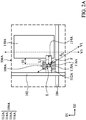
- the transistor 108A includes a source electrode 112A, a drain electrode 114A, a gate electrode 116A and a channel 118A.
- the source electrode 112A and the drain electrode 114A may be disposed on two opposite sides of the gate electrode 116A.
- the channel 118A may be formed between the source electrode 112A and the drain electrode 114A.
- the drain electrode 114A may be electrically connected to the modulating electrode 110A.
- the transistor 108B includes a source electrode 112B, a drain electrode 114B, a gate electrode 116B and a channel 118B.
- the source electrode 112B and the drain electrode 114B are disposed on two opposite sides of the gate electrode 116B.
- the channel 118B may be formed between the source electrode 112B and the drain electrode 114B.
- the drain electrode 114B may be electrically connected to the modulating electrode 110B.
- the source electrode 112B, the gate electrode 116B and the channel 118B of the modulating unit 106B may respectively be the same as or similar to the source electrode 112A, the gate electrode 116A and the channel 118A of the modulating unit 106A.
- one of the differences between the modulating unit 106A and the modulating unit 106B is that the included angles between the extending direction of the channel and the longitudinal direction of the modulating electrode.
- direction V1 and direction V2 can respectively be regarded as the extending directions of channel 118A and channel 118B.
- the direction V1 of channel 118A and the direction V2 of channel 118B may be substantially parallel.
- the extending direction of the channel may be a direction determined by two reference points respectively on the drain electrode and the source electrode. The two reference points may be overlapped with the channel.
- the direction V1 of channel 118A may be determined by reference point E on the source electrode 112A and reference point F on the drain electrode 114A.
- the direction V2 of channel 118B may be determined by a reference point G on the source electrode 112B and a reference point H on the drain electrode 114B.
- the positions of the reference points E and F of the modulating unit 106A may correspond to the reference points G and H of the modulating unit 106B so that direction V1 may be substantially parallel to direction V2.
- the modulating electrode 110A may have a rectangular shape.
- the longitudinal direction of the modulating electrode 110A may be substantially parallel to the long side of the modulating electrode 110A.
- the longitudinal direction of the modulating electrode 110B may be substantially parallel to the long side of the modulating electrode 110B.
- direction V3 which may be substantially parallel to the long side of the modulating electrode 110A, may be the longitudinal direction of modulating electrode 110A.
- Direction V4 which may be substantially parallel to the long side of the modulating electrode 110B, may be the longitudinal direction of modulating electrode 110B.
- the longitudinal direction of modulating electrode 110B (direction V4) may be different from the longitudinal direction of modulating electrode 110A (direction V3).
- the first included angle ⁇ A between the direction V1 and the direction V3 is different from a second included angle ⁇ B between the direction V2 and the direction V4. That is, the included angle between the extending direction of the transistor 108A and the longitudinal direction of the modulating electrode 110A of the modulating unit 106A may be different from the included angle between the extending direction of the transistor 108B and the longitudinal direction of the modulating electrode 110B of the modulating unit 106B. Because the longitudinal direction of the modulating electrode influences on the orientation of the modulating medium, the orientation of the modulating medium of the modulating unit 106A may be different from the orientation of the modulating medium of the modulating unit 106B.
- the orientation of the modulating medium may vary in accordance with the included angles of the modulating unit.
- the direction V1 may be parallel to the direction V2 so that the variance of the lithography and/or etching process for forming the components of the modulating unit 106A and the modulating unit 106B may be reduced.
- the difference between the width-to-length ratios of the channel 118A and the channel 118B may also be reduced.
- the difference between the first included angle ⁇ A and the second included angle ⁇ B may be greater than 15 degrees.
- the difference between the first included angle ⁇ A and the second included angle ⁇ B may be in a range from 15 degrees to 90 degrees, such as 30 degrees or 60 degrees.
- the difference between the first included angle ⁇ A and the second included angle ⁇ B may be in a range from 45 degrees to 90 degrees.
- the difference between the first included angle ⁇ A and the second included angle ⁇ B may not be less than 15 degrees. If the difference between the first included angle ⁇ A and the second included angle ⁇ B is less than 15 degrees, the information emitted by the electronic device may be affected when the receiver is located in an undesired location.
- the included angles of the extending direction of the channel and the longitudinal direction of modulating electrode may include an acute angle and an obtuse angle.
- the first included angle ⁇ A and the second included angle ⁇ B may be referred to the acute angle. But the present disclosure is not limited thereto.
- the length L1 of the drain electrode 114A may be different from the length L2 of the drain electrode 114B due to different extending directions of the modulating electrode 110A and the modulating electrode 110B.
- the lengths L1 and L2 may be measured along the second direction D2 (e.g. the X-direction).
- the distance S1 between the channel 118A and the modulating electrode 110A may be different from the distance S2 between the channel 118B and the modulating electrode 110B.
- the distances S1 and S2 may be measured along the second direction (e.g. the X-direction). It should be understood that the distances S1 and S2 can be defined as a minimum distance between the channel and the modulating electrode, and the distances S1 and S2 are not limited to be measured along the second direction D2 but measured along the same direction.
- FIGs. 2A and 2B illustrate that each of the source electrode, the drain electrode, and the channel has a rectangular shape. Many variations and/or modifications can be made to embodiments of the disclosure.
- the modulating unit 106C includes a transistor 108C and a modulating electrode 110C.
- the transistor 108C may have a source electrode 112C, a drain electrode 114C, a gate electrode 116C, a channel 118C and an semiconductor layer 120C.
- the channel 118C may be disposed between the source electrode 112C and the drain electrode 114C.
- the channels shown in the figures of the present disclosure are only for exemplary illustration and not intended to limit the scope of the present disclosure.
- the people having ordinary skill in the art should know the range of the channel region in practice. The details will not be described herein.
- the source electrode 112C and the drain electrode 114C respectively have multiple protruding portions 122 and 124 so that the channel 118C may have a bent shape.
- the extending direction of the channel 118C may be defined by two reference points located on the source electrode 112C and the drain electrode 114C, respectively. These two reference points can be chosen arbitrarily from the source electrode 112C and the drain electrode 114C overlapping the channel 118C.
- the direction V5 which may be determined by a reference point K on the source electrode 112C and a reference point L on the drain electrode 114C, can be defined as an extending direction of the channel 118C.
- the direction V6, which may be determined by a reference point K on the source electrode 112C and a reference point M on the drain electrode 114C can also be chosen to define an extending direction of the channel 118C.
- the positions of the reference points used to define the extending direction of one transistor are the same as or corresponding to those of another transistor.
- the extending directions of the channels in the transistors of at least two of the modulating units may be substantially parallel. More specifically, the included angles between the extending direction of the transistor and the longitudinal direction of the modulating electrode may vary in accordance with the longitudinal direction of the respective modulating electrodes.
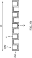
- the extending direction of the transistor may be defined in other ways. As shown in FIG. 3B , there is the smallest imaginary rectangle Z1 that can encircle the channel 118C. In this embodiment, the extending direction of the channel 118C may be referred to the extending direction of the imaginary rectangle Z1, such as the direction of the long side of the imaginary rectangle Z1.
- the width-to-length ratio of the channel 118C may be defined as the ratio of the width W of the channel 118C to the length L3.
- the width W of the channel 118C may be the total length of the channel 118C.
- the length L3 may be the length of the long side of the imaginary rectangle Z1.
- a modulating unit 106D includes a transistor 108D and a modulating electrode 110D.
- the transistor 108D may include a source electrode 112D, a drain electrode 114D, a gate electrode 116D, a channel 118D and a semiconductor layer 120D that is disposed between the source electrode 112D and the gate electrode 116D.
- the shapes of the source electrode 112D and the drain electrode 114D are different from the shapes of the source electrode 112C and the drain electrode 114D of FIG. 3A .
- the channel 118D has a width-to-length ratio different from the channel 118C.
- the extending direction of the channel 118D may be defined by two reference points located on the source electrode 112D and the drain electrode 114D, respectively.
- the gate electrode 116D and the semiconductor layer 120D forms an overlapping region.
- These two reference points can be chosen arbitrarily from the source electrode 112D and the drain electrode 114D in the overlapping region.
- the direction V8 which may be determined by a reference point P on the source electrode 112D and a reference point Q on the drain electrode 114D, may be regarded as the extending direction of the channel 118D.
- the extending direction of the transistor may be defined in other ways. As shown in FIG. 4B , there is the smallest imaginary rectangle Z2 that can encircle the channel 118D. In this embodiment, the extending direction of the channel 118D may be referred to the extending direction of the imaginary rectangle Z2, such as the direction of the long side of the imaginary rectangle Z2.
- the width-to-length ratio of the channel 118D may be defined as the ratio of the width W of the channel 118D to the length L4.
- the width W of the channel 118D may be the total length of the channel 118D.
- the length L3 may be the length of the long side of the imaginary rectangle Z2.
- the modulating electrode 110E has a rectangular shape.
- the direction V10 which may be parallel to the long side of the modulating electrode 110E, may be defined as a longitudinal direction of the modulating electrode 110E.
- the modulating electrode 110F may have an irregular shape.
- FIG. 5B illustrates the smallest imaginary rectangle Z3 that can encircle the modulating electrode 110F.
- direction V11 which may be parallel to the long side of the imaginary rectangle Z3, can be regarded as the longitudinal direction of the modulating electrode 110F.
- the smallest imaginary rectangle mentioned above can be obtained by software such as OpenCV or other suitable software.
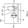
- a modulating unit 106G includes transistor 108G and a modulating electrode 110G.
- the transistor 108G includes a drain electrode 114G electrically connected to the modulating electrode 110G.
- the drain electrode 114G and the modulating electrode 110G form an overlapping region Z5.
- a ratio of the area of the overlapping region Z5 to the area of the modulating electrode 110G may be in a range from 5% to 50%, such as 15% or 35%.
- the ratio of the area of the overlapping region Z5 to the area of the modulating electrode 110G may be in a range from 5% to 20%. If the ratio of the area of the overlapping region Z5 to the area of the modulating electrode 110G is in a range from 5% to 50%, the charging speed of the modulating electrode may be improved.
- a third included angle ⁇ 3 between the longitudinal direction of the overlapping region Z5 and the longitudinal direction of the modulating electrode 110G there is a third included angle ⁇ 3 between the longitudinal direction of the overlapping region Z5 and the longitudinal direction of the modulating electrode 110G.
- the direction V12 can be regarded as the longitudinal direction of the overlapping region Z5
- the direction V13 can be regarded as the longitudinal direction of the modulating electrode 110G.
- the third included angle ⁇ 3 between the longitudinal direction of the overlapping region Z5 and the longitudinal direction of the modulating electrode 110G may be 90 degrees.
- a third included angle ⁇ 3 between the longitudinal direction of the overlapping region Z5 and the longitudinal direction of the modulating electrode 110G may range from 70 degrees to 110 degrees, such as 80 degrees, 90 degrees, or 100 degrees.
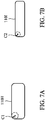
- a modulating electrode 110H and a modulating electrode 110I of the electronic modulating device may have different areas and shapes.
- the profile of the modulating electrode 110H and modulating electrode 1101 may have rounded corners. The rounded corner may assist in decreasing the aggregation of electrons at a sharp point. As a result, electrostatic discharge (ESD) can be reduced.
- ESD electrostatic discharge
- the radius of curvature C1 of the corners of the modulating electrode 110H may be different from the radius of curvature C2 of the corners of the modulating electrode 110H.
- the radius of curvature C1 may be greater than the radius of curvature C2.
- FIG. 8 illustrates a cross-sectional view of an electronic modulating device 200 in accordance with some embodiments of the present disclosure. It should be understood that some of the components of the electronic modulating device 200 are omitted in FIG. 8 for clarity. It also should be understood that additional components may be added to the electronic modulating device 200 in accordance with some embodiments of the present disclosure. Some of the components described below may be replaced or eliminated in accordance with some embodiments of the present disclosure.
- the electronic modulating device 200 includes a first substrate 202.
- the first substrate 202 may be used as the support for the transistor, modulating electrode and other components.
- the first substrate 202 may include a glass substrate, a ceramic substrate, a plastic substrate, and/or other applicable substrates.
- a gate insulator layer 204 and a passivation layer 206 are formed on the first substrate 202.
- the gate insulator layer 204 may include, but is not limited to, silicon dioxide or high dielectric constant (high-k) material, phosphosilicate glass (PSG), borophosphosilicate glass (BPSG), low dielectric constant (low-k) dielectric material and other applicable dielectric materials.
- the low dielectric constant dielectric materials include, but are not limited to, fluorinated silica glass (FSG), carbon doped silicon oxide, amorphous fluorinated carbon, parylene, bis-benzocyclobutenes (BCB), polyimides, combinations of the above-mentioned materials, and other applicable materials.
- FSG fluorinated silica glass
- carbon doped silicon oxide amorphous fluorinated carbon
- parylene parylene
- bis-benzocyclobutenes (BCB) bis-benzocyclobutenes
- polyimides combinations of the above-mentioned materials, and other applicable materials.
- the gate insulator layer 204 and the passivation layer 206 may be formed by a deposition process such as chemical vapor deposition, physical vapor deposition or other suitable deposition process.
- the electronic modulating device 200 includes a transistor 208 that is formed on the first substrate 202.
- the transistor 208 includes a source electrode 210, a drain electrode 212, a gate electrode 214, and a semiconductor layer 216.
- the gate electrode 214 may be disposed on the first substrate 202.
- the gate electrode 214 may include metal materials.
- the gate electrode 214 may include, but is not limited to, copper (Cu), aluminum (Al), molybdenum (Mo), tungsten (W), gold (Au), chromium (Cr), nickel (Ni), platinum (Pt), titanium (Ti).
- the gate electrode 214 may be formed by, but is not limited to, a sputter process.
- the semiconductor layer 216 may be disposed on the gate insulator layer 204.
- the material of the semiconductor layer 216 may include, but is not limited to, amorphous silicon, polysilicon such as low-temp polysilicon (LTPS), metal oxide or other suitable materials.
- the metal oxide may include indium gallium zinc oxide (IGZO), indium zinc oxide (IZO), indium gallium zinc tin oxide (IGZTO).
- the source electrode 210 and the drain electrode 212 may be formed on the gate insulator layer 204.
- the source electrode 210 and the drain electrode 212 may be disposed on the gate electrode 214 and on two sides of the gate electrode 214.
- portions of the source electrode 210 and the drain electrode 212 are formed on the semiconductor layer 216.
- the materials and formation methods of the source electrode 210 and the drain electrode 212 may be the same as or similar to those of the gate electrode 214. As shown in FIG. 8 , the channel 218 may be formed in the gate insulator layer 204 and between the source electrode 210 and the drain electrode 212. It is noted that the structure of the transistor described herein is only for illustration, and it may use other suitable structures of the transistors, such as a top-gate transistor.
- the gate insulator layer 204 illustrated in FIG.8 may be disposed on the gate electrode 214.
- the gate electrode 214 may be formed on the passivation layer 206 and in the same horizontal layer as a modulating electrode 222.
- the electronic modulating device 200 includes two gate electrodes where these two gate electrodes are located on the same horizontal layer. For example, these two gate electrodes may be formed on the first substrate 202.
- the electronic modulating device 200 includes two gate electrodes where these two gate electrodes are disposed on different horizontal layers. For example, one of the gate electrodes is disposed on the first substrate 202, and one of the other is disposed on the passivation layer 206.
- the electronic modulating device 200 includes a conductive element 220 and a modulating electrode 222.
- the modulating electrode 222 may be electrically connected to the drain electrode 212 through the conductive element 220.
- the materials of the conductive element 220 and the modulating electrode 222 may be the same as or similar to the material of the gate electrode 214.
- a lithography process and an etching process are performed on the passivation layer 206 to form an opening.
- a metal material is filled into the opening and deposited on the passivation layer 206 followed by performing a lithography process and an etching process to pattern the metal material disposed on the passivation layer 206.
- the photolithography process includes, but is not limited to, photoresist coating (e.g., spin-on coating), soft baking, mask alignment, exposure, post-exposure baking, developing the photoresist, rinsing and drying (e.g., hard baking).
- the photolithography process may also be implemented or replaced by other proper processes, such as a maskless photolithography process, an electron-beam process, an ion-beam process, or a combination thereof.
- the etching process may include, but is not limited to, a dry etching process, a wet etching process, and/or a combination thereof.
- the electronic modulating device 200 includes a second substrate 224.
- the second substrate 224 may be configured to dispose a common electrode and/or other components.
- the second substrate 224 may include a glass substrate, a ceramic substrate, a plastic substrate and/or other applicable substrates.
- a display element layer 226 may be formed on the second substrate 224.
- the display element layer 226 may include, but is not limited to, a color filter layer, a light shielding layer, a passivation layer, and other applicable components or layers.
- a common electrode 228 may be formed on the second substrate 224.
- the material and formation method of the common electrode 228 may be the same as or similar to those of the gate electrode 214.
- FIG. 8 illustrates that the common electrode 228 may be non-patterned. Many variations and/or modifications can be made to embodiments of the disclosure. In some embodiments, the common electrode 228 may be patterned so that the common electrode 228 has discrete portions.
- the electronic modulating device 200 may further include a spacer 230 and a modulating medium layer 232.
- the modulating medium layer 232 may be disposed between the modulating electrode 222 and the common electrode 228.
- the modulating medium layer 232 may include a liquid crystal layer or other suitable layers.
- the spacer 230 may be configured to determine the cell gap between the first substrate 202 and the second substrate 224.
- the spacer 230 may include, but is not limited to, polyethylene terephthalate (PET), polyethylene (PE), polyethersulfone (PES), polycarbonate (PC), polymethylmethacrylate (PMMA), glass, any other suitable materials, or a combination thereof.
- the potential difference between the modulating electrode 222 and the common electrode 228 may determine the orientation of the modulating medium layer 232.
- the voltage of the modulating electrode 222 can be controlled by the transistor 208 so that the orientation of the modulating medium layer 232 varied in accordance with the voltage of the modulating electrode 222.
- the modulating medium layer 232 may be applied in different liquid-crystal mode in accordance with the structure of the electrode or orientation of the polyimide layer.
- the material of the modulating medium layer 232 may be, but is not limited to, a nematic liquid crystal, a smectic liquid crystal, a cholesteric liquid crystal, a blue phase liquid crystal, or any other applicable liquid-crystal material.
- a ratio of the length L5 to the length L6 of the modulating electrode 222 may be in a range from 30% to 90%, such as 50% or 70%. If the ratio of the length L5 to the length L6 of the modulating electrode 222 is in a range from 30% to 90%, the resistance of the electronic modulating device 200 can be reduced.
- the length L5 and the length L6 may be measured along the longitudinal direction of the modulating electrode 222. However, the length L5 and the length L6 may be measured along other directions, and the scope of the disclosure is not intended to be limited.
- the electronic modulating device 300 includes a first electrode 234 disposed on the first substrate 202 and a second electrode 236 disposed on the second substrate 224.
- the modulating electrode 222' may be disposed between the first electrode 234 and the second electrode 236, and electrically connected to the drain electrode 212 through the conductive element 220'.
- the materials and the formation method of the conductive element 220', the modulating electrode 222', the first electrode 234 and the second electrode 236 are the same as or similar to those of the modulating electrode 222, and are not repeated herein.
- the first electrode 234 may be separated from the second electrode 236 by the spacer 230 and a cavity 238.
- the cavity 238 may include, but is not limited to, air or oil.
- the voltages of the first electrode 234 and the second electrode 236 may be fixed.
- the voltage of the modulating electrode 222' may be controlled by the transistor 208.
- the modulating electrode 222' may shift correspondingly.
- the capacitance between the second electrode 236 and the modulating electrode 222', or the capacitance between the first electrode 234 and the modulating electrode 222' may vary correspondingly. Therefore, the electro-magnetic radiation (e.g. the light) having a different wavelength can be emitted from and/or received by the electronic modulating device 300.
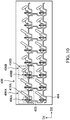
- the electronic modulating device 400 includes a plurality of data lines 402 and scan lines 404. At least one of the data lines 402 may extend along the first direction D1, and at least one of the scan lines 404 may extend along the second direction D2 different from the first direction D1.
- the electronic modulating device 400 also includes a modulating unit 406A and a modulating unit 406B.
- the modulating unit 406A includes a transistor 408A and a modulating electrode 410A.
- the modulating unit 406B includes a transistor 408B and a modulating electrode 410B.
- the area of the modulating electrode 410A may be different from that of the modulating electrode 410B.
- the radius of the curvature at the corner of the modulating electrode 410A may be different from the radius of the modulating electrode 410B.
- the longitudinal direction of the modulating electrode 410A may be different from longitudinal direction of the modulating electrode 410B.
- the included angle between the extending direction of the channel in the transistor 408A and the longitudinal direction of the modulating electrode 410A may be different from the included angle between the extending direction of the channel in the transistor 408B and the longitudinal direction of the modulating electrode 410B.
- the arrangement of the modulating unit 406A and the modulating unit 406B shown in FIG. 10 may be modified.
- the arrangement of the modulating unit 406A and the modulating unit 406B may be the same as that shown in FIG. 1 , and the scope of the disclosure is not intended to be limited.
- the size of the modulating electrode 410A of the modulating unit 406A may be different from the size of the modulating electrode 410B and the modulating unit 406B.
- different sizes of the modulating electrodes may correspond to different width-to-length ratios of the channels. But the present disclosure is not limited thereto.
- At least one of the data lines 402 and at least one of the scan lines 404 may have wave shapes. Therefore, the electronic modulating device 400 may be applied in bending electronic device. Moreover, the included angles between different channels of the transistors (such as the modulating unit 406A and the modulating unit 406B) and the data line 402 (or scan line 404) may be substantially the same.
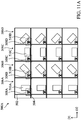
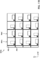
- FIGs. 11A-11D illustrate top views of the electronic modulating devices in accordance with some embodiments of the present disclosure.
- FIGs. 11A-11D illustrate the different arrangements of the transistors and the modulating electrodes.
- the scope of the disclosure is not intended to be limited.
- the electronic modulating device 500A includes modulating units 506A, 506B, 506C and 506D.
- the transistors modulating units 506A, 506B, 506C and 506D respectively include one transistor 508A, 508B, 508C and 508D and one modulating electrode 510A, 510B, 510C and 510D.
- the extending directions of the channels of the transistors 508A, 508B, 508C and 508D may be substantially parallel to each other.
- the longitudinal directions of the modulating electrodes 510A, 510B, 510C and 510D may be different from each other.
- the included angles between the extending direction of the channels of the transistors and the longitudinal directions of the modulating electrodes of the modulating units 506A, 506B, 506C and 506D may be different from each other.
- some of the modulating units 506A, 506B, 506C and 506D may be arranged along the first direction D1.
- Many variations and/or modifications can be made to embodiments of the disclosure.
- some of the modulating units 506A, 506B, 506C and 506D may be arranged along the second direction D2.
- the electronic modulating device 500B includes a plurality of modulating units 506A and modulating units 506C.
- the modulating units 506A and the modulating units 506C are alternately arranged along the second direction D2.
- the modulating unit 506A and the modulating unit 506C are alternately arranged along the first direction D1.
- the electronic modulating device 500C includes the plurality of modulating units 506A and the modulating units 506C.
- the four modulating units 506A can be classified to a group G1 which is a 2 ⁇ 2 array
- the four modulating units 506C can be classified to a group G2 which is a 2 ⁇ 2 array.
- the group G1 and the group G2 may be alternately arranged along the second direction D2.
- the group G1 and the group G2 may be alternately arranged along the first direction D1.
- the groups G1 and/or G2 may be an m ⁇ m array, wherein m is greater than 2.
- the groups G1 and/or G2 may be an m ⁇ n array, wherein m and n are greater than or equivalent to 2, m and n are positive integers, and m ⁇ n. Furthermore, the group G1 and/or the group G2 may be an oblique square m ⁇ m array.
- the electronic modulating device 500D includes the plurality of groups G3 and groups G4 that are 2 ⁇ 2 arrays.
- the group G3 and the group G4 may be alternately arranged along the second direction D2 and the first direction D1.
- the group G3 may consist of three modulating unit 506A and one modulating unit 506B.
- the group G4 may consist of three modulating unit 506C and one modulating unit 506D.
- the scope of the disclosure is not intended to be limited.
- the electronic modulating device may include a different arrangement for the electronic units.
- the area of the modulating electrodes may be altered.
- the width-to-length ratio of the channel of the transistor may be fine-tuned in accordance with the area of the modulating electrodes.
- the present disclosure provides an electronic modulating device.
- the electronic modulating device has electronic units that have different included angles.
- the included angle may be between the extending direction of the channel of the transistor and the longitudinal direction of the modulating electrode.
- the information emitted by the electronic device may not be affected when the receiver is located in an undesired location.
- the electronic modulating device of the embodiments can be applied in the structure of microelectromechanical system (MEMS), antenna system, or display device, and the scope of the disclosure is not intended to be limited.
- MEMS microelectromechanical system
Landscapes
- Physics & Mathematics (AREA)
- Nonlinear Science (AREA)
- General Physics & Mathematics (AREA)
- Chemical & Material Sciences (AREA)
- Crystallography & Structural Chemistry (AREA)
- Mathematical Physics (AREA)
- Optics & Photonics (AREA)
- Engineering & Computer Science (AREA)
- Geometry (AREA)
- Computer Hardware Design (AREA)
- Theoretical Computer Science (AREA)
- Thin Film Transistor (AREA)
- Liquid Crystal (AREA)
- Devices For Indicating Variable Information By Combining Individual Elements (AREA)
Abstract
Description
- The present disclosure relates to an electronic modulating device, and in particular to an electronic modulating device that includes different arrangements of modulating electrodes.
- Electronic products that include a display panel, such as smartphones, tablets, notebooks, monitors, and TVs, have become indispensable necessities in modern society. With the flourishing development of such portable electronic products, consumers have high expectations regarding the quality, functionality, and price of such products. These electronic products are often provided with communications capabilities. However, the communications capabilities still need to be improved.
- In accordance with some embodiments of the present disclosure, an electronic modulating device is provided. The electronic modulating device includes a first modulating unit. The first modulating unit includes a first transistor including a channel arranged in an extending direction. The first modulating unit also includes a first modulating electrode electrically connected to the first transistor and arranged in a first longitudinal direction. The electronic modulating device also includes a second modulating unit. The second modulating unit includes a second transistor including a channel arranged in the extending direction. The second modulating unit also includes a second modulating electrode electrically connected to the second transistor and arranged in a second longitudinal direction that is different from the first longitudinal direction. The first included angle between the extending direction and the first longitudinal direction is different from a second included angle between the extending direction and the second longitudinal direction.
- In accordance with some embodiments of the present disclosure, an electronic modulating device is provided. The electronic modulating device includes a first modulating unit. The first modulating unit includes a first transistor including a channel. The first modulating unit also includes a first modulating electrode electrically connected to the first transistor. The electronic modulating device also includes a second modulating unit. The second modulating unit includes a second transistor including a channel. The second modulating unit also includes a second modulating electrode electrically connected to the second transistor. A distance between the channel of the first transistor and the first modulating electrode is different from a distance between the channel of the second transistor and the second modulating electrode
- A detailed description is given in the following embodiments with reference to the accompanying drawings.
- The disclosure may be understood by reading the subsequent detailed description and examples with references made to the accompanying drawings, wherein:
-
FIG. 1 illustrates a top view of the electronic modulating device in accordance with some embodiments of the present disclosure. -
FIGs. 2A and2B illustrate enlarged top views of a modulating unit in the electronic modulating device in accordance with some embodiments of the present disclosure. -
FIGs. 3A and3B illustrate examples of the definition of the extending direction of a channel in the electronic modulating device in accordance with some embodiments of the present disclosure. -
FIGs. 4A and 4B illustrate examples of the definition of the extending direction of the channel in the electronic modulating device in accordance with some embodiments of the present disclosure. -
FIGs. 5A and 5B illustrate examples of the definition of the longitudinal direction of a modulating electrode in the electronic modulating device in accordance with some embodiments of the present disclosure. -
FIG. 6 illustrates enlarged top views of the modulating unit in the electronic modulating device in accordance with some embodiments of the present disclosure. -
FIGs. 7A and 7B illustrate examples of the modulating electrodes in the electronic modulating device in accordance with some embodiments of the present disclosure. -
FIG. 8 illustrates a cross-sectional view of the electronic modulating device in accordance with some embodiments of the present disclosure. -
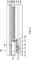
FIG. 9 illustrates a cross-sectional view of the electronic modulating device in accordance with some embodiments of the present disclosure. -
FIG. 10 illustrates a top view of the electronic modulating device in accordance with some embodiments of the present disclosure. -
FIGs. 11A-11D illustrates a top view of the electronic modulating device in accordance with some embodiments of the present disclosure. - The electronic modulating device of the present disclosure and the manufacturing method thereof are described in detail in the following description. In the following detailed description, for purposes of explanation, numerous specific details and embodiments are set forth in order to provide a thorough understanding of the present disclosure. It will be apparent, however, that the exemplary embodiments set forth herein are used merely for the purpose of illustration, and the inventive concept may be embodied in various forms without being limited to those exemplary embodiments. In addition, the drawings of different embodiments may use like and/or corresponding numerals to denote like and/or corresponding elements. However, the use of like and/or corresponding numerals in the drawings of different embodiments does not suggest any correlation between different embodiments. In addition, in this specification, expressions such as "first material layer disposed above/on/over a second material layer", may indicate the direct contact of the first material layer and the second material layer, or it may indicate a noncontact state with one or more intermediate layers between the first material layer and the second material layer. In the above situation, the first material layer may not be in direct contact with the second material layer.
- In addition, in this specification, relative expressions are used. For example, "upper" or "lower" is used to describe the position of one element relative to another. It should be appreciated that if a device is flipped upside down, an element that is on the "bottom" will become an element that is on the "top".
- It should be understood that, although the terms first, second, third etc. may be used herein to describe various elements, components, regions, layers, portions and/or sections, these elements, components, regions, layers, portions and/or sections should not be limited by these terms. These terms are only used to distinguish one element, component, region, layer, portion or section from another element, component, region, layer or section. Thus, a first element, component, region, layer, portion or section discussed below could be termed a second element, component, region, layer, portion or section without departing from the teachings of the present disclosure.
- It should be understood that this description of the exemplary embodiments is intended to be read in connection with the accompanying drawings, which are to be considered part of the entire written description. The drawings are not drawn to scale. In addition, structures and devices are shown schematically in order to simplify the drawing.
- The terms "about" and "substantially" typically mean +/- 20% of the stated value, more typically +/- 10% of the stated value, more typically +/- 5% of the stated value, more typically +/- 3% of the stated value, more typically +/- 2% of the stated value, more typically +/- 1% of the stated value and even more typically +/- 0.5% of the stated value. The stated value of the present disclosure is an approximate value. When there is no specific description, the stated value includes the meaning of "about" or "substantially". Moreover, when considering the deviation or the fluctuation of the manufacturing process, the term "same" may also include the meaning of "about" or "substantially"
- Unless defined otherwise, all technical and scientific terms used herein have the same meaning as commonly understood by one of ordinary skill in the art to which this disclosure belongs. It should be appreciated that, in each case, the term, which is defined in a commonly used dictionary, should be interpreted as having a meaning that conforms to the relative skills of the present disclosure and the background or the context of the present disclosure, and should not be interpreted in an idealized or overly formal manner unless so defined.
- In addition, in some embodiments of the present disclosure, terms concerning attachments, coupling and the like, such as "connected" and "interconnected," refer to a relationship wherein structures are secured or attached to one another either directly or indirectly through intervening structures, as well as both movable or rigid attachments or relationships, unless expressly described otherwise.
- In addition, the term "longitudinal direction" is defined as the direction along or parallel to the long axis of an object. The long axis is defined as a line extending through the center of an object lengthwise. For an elongated or oblong object, the long axis corresponds most nearly to its greatest dimension lengthwise. For an object that does not have a definite long axis, the long axis is the long axis of the smallest rectangle that can encompass the object.
- In addition, the phrase "in a range from a first value to a second value" indicates the range includes the first value, the second value, and other values in between.
- In accordance with some embodiments of the present disclosure, an electronic modulating device is provided. The electronic modulating device has electronic units that have different included angles between the extending direction of the channel of the transistor and the longitudinal direction of the modulating electrode. Thus, there are fewer variations of the information received at different directions from the electronic modulating device.
-
FIG. 1 illustrates a top view of anelectronic modulating device 100 in accordance with some embodiments of the present disclosure. It should be understood that some of the components of theelectronic modulating device 100 are omitted inFIG. 1 for clarity. It also should be understood that additional components may be added to theelectronic modulating device 100 in accordance with some embodiments of the present disclosure. Some of the components described below may be replaced or eliminated in accordance with some embodiments of the present disclosure. - As illustrated in
FIG. 1 , theelectronic modulating device 100 includes a plurality ofdata lines 102 andscan lines 104. At least one of thedata lines 102 may extend along a first direction D1 (e.g. the Y-direction), and at least one of thescan lines 104 may extend along a second direction D2 (e.g. the X-direction) different from the first direction D1. The data lines 102 and thescan lines 104 may define a plurality of modulating units or pixels. In some embodiments, theelectronic modulating device 100 includes a plurality of modulatingunits 106A and modulatingunits 106B that are electrically connected to thedata lines 102 and thescan lines 104, respectively. For example, the source electrodes of some of the modulatingunits 106A and the modulatingunits 106B may be electrically connected to the data lines 102. For another example, the gate electrodes of some of the modulatingunits 106A and the modulatingunits 106B may be electrically connected to the scan lines 104. In addition, the modulatingunits 106A and/or the modulatingunits 106B may be both arranged along the first direction D1. Many variations and/or modifications can be made to embodiments of the disclosure. In some embodiments, modulatingunits 106A and/or modulatingunits 106B may be both arranged along the second direction D2. - As shown in
FIG. 1 , at least one of the modulatingunits 106A includes atransistor 108A and a modulatingelectrode 110A, and at least one of the modulatingunits 106B includes atransistor 108B and a modulatingelectrode 110B. In some embodiments, the orientation of the modulating medium (such as liquid crystals) of theelectronic modulating device 100 can be controlled by adjusting the capacitance between the modulating electrode (110A and 110B) and a common electrode (shown inFIG.8 ) so that the electro-magnetic radiation (e.g. light) having a different wavelength can be emitted from and/or received by theelectronic modulating device 100. - Refer to
FIGs. 2A and2B , which illustrate enlarged top views of the modulatingunit 106A and the modulatingunit 106B in accordance with some embodiments of the present disclosure. As shown inFIG. 2A , thetransistor 108A includes asource electrode 112A, adrain electrode 114A, agate electrode 116A and achannel 118A. The source electrode 112A and thedrain electrode 114A may be disposed on two opposite sides of thegate electrode 116A. Thechannel 118A may be formed between thesource electrode 112A and thedrain electrode 114A. Moreover, thedrain electrode 114A may be electrically connected to the modulatingelectrode 110A. - As shown in
FIG. 2B , thetransistor 108B includes asource electrode 112B, adrain electrode 114B, agate electrode 116B and achannel 118B. The source electrode 112B and thedrain electrode 114B are disposed on two opposite sides of thegate electrode 116B. Thechannel 118B may be formed between thesource electrode 112B and thedrain electrode 114B. Moreover, thedrain electrode 114B may be electrically connected to the modulatingelectrode 110B. Thesource electrode 112B, thegate electrode 116B and thechannel 118B of the modulatingunit 106B may respectively be the same as or similar to thesource electrode 112A, thegate electrode 116A and thechannel 118A of the modulatingunit 106A. - In some embodiments, one of the differences between the modulating
unit 106A and the modulatingunit 106B is that the included angles between the extending direction of the channel and the longitudinal direction of the modulating electrode. In some embodiments, as shown inFIGs. 2A and2B , direction V1 and direction V2 can respectively be regarded as the extending directions ofchannel 118A andchannel 118B. Moreover, the direction V1 ofchannel 118A and the direction V2 ofchannel 118B may be substantially parallel. The extending direction of the channel may be a direction determined by two reference points respectively on the drain electrode and the source electrode. The two reference points may be overlapped with the channel. - For example, as shown in
FIG. 2A , the direction V1 ofchannel 118A may be determined by reference point E on thesource electrode 112A and reference point F on thedrain electrode 114A. Similarly, the direction V2 ofchannel 118B may be determined by a reference point G on thesource electrode 112B and a reference point H on thedrain electrode 114B. More specifically, the positions of the reference points E and F of the modulatingunit 106A may correspond to the reference points G and H of the modulatingunit 106B so that direction V1 may be substantially parallel to direction V2. - In some embodiments, the modulating
electrode 110A may have a rectangular shape. The longitudinal direction of the modulatingelectrode 110A may be substantially parallel to the long side of the modulatingelectrode 110A. Similarly, the longitudinal direction of the modulatingelectrode 110B may be substantially parallel to the long side of the modulatingelectrode 110B. In this embodiment, direction V3, which may be substantially parallel to the long side of the modulatingelectrode 110A, may be the longitudinal direction of modulatingelectrode 110A. Direction V4, which may be substantially parallel to the long side of the modulatingelectrode 110B, may be the longitudinal direction of modulatingelectrode 110B. As shown inFIGs. 2A and2B , the longitudinal direction of modulatingelectrode 110B (direction V4) may be different from the longitudinal direction of modulatingelectrode 110A (direction V3). - In some embodiments, as shown in
FIGs. 2A and2B , the first included angle θA between the direction V1 and the direction V3 is different from a second included angle θB between the direction V2 and the direction V4. That is, the included angle between the extending direction of thetransistor 108A and the longitudinal direction of the modulatingelectrode 110A of the modulatingunit 106A may be different from the included angle between the extending direction of thetransistor 108B and the longitudinal direction of the modulatingelectrode 110B of the modulatingunit 106B. Because the longitudinal direction of the modulating electrode influences on the orientation of the modulating medium, the orientation of the modulating medium of the modulatingunit 106A may be different from the orientation of the modulating medium of the modulatingunit 106B. That is, the orientation of the modulating medium may vary in accordance with the included angles of the modulating unit. Moreover, the direction V1 may be parallel to the direction V2 so that the variance of the lithography and/or etching process for forming the components of the modulatingunit 106A and the modulatingunit 106B may be reduced. Furthermore, the difference between the width-to-length ratios of thechannel 118A and thechannel 118B may also be reduced. - In some embodiments, the difference between the first included angle θA and the second included angle θB may be greater than 15 degrees. For example, the difference between the first included angle θA and the second included angle θB may be in a range from 15 degrees to 90 degrees, such as 30 degrees or 60 degrees. In some embodiments, the difference between the first included angle θA and the second included angle θB may be in a range from 45 degrees to 90 degrees. In some cases, the difference between the first included angle θA and the second included angle θB may not be less than 15 degrees. If the difference between the first included angle θA and the second included angle θB is less than 15 degrees, the information emitted by the electronic device may be affected when the receiver is located in an undesired location. It is noted that the included angles of the extending direction of the channel and the longitudinal direction of modulating electrode may include an acute angle and an obtuse angle. The first included angle θA and the second included angle θB may be referred to the acute angle. But the present disclosure is not limited thereto.
- In some embodiments, as shown in
FIGs. 2A and2B , the length L1 of thedrain electrode 114A may be different from the length L2 of thedrain electrode 114B due to different extending directions of the modulatingelectrode 110A and the modulatingelectrode 110B. The lengths L1 and L2 may be measured along the second direction D2 (e.g. the X-direction). In some embodiments, the distance S1 between thechannel 118A and the modulatingelectrode 110A may be different from the distance S2 between thechannel 118B and the modulatingelectrode 110B. The distances S1 and S2 may be measured along the second direction (e.g. the X-direction). It should be understood that the distances S1 and S2 can be defined as a minimum distance between the channel and the modulating electrode, and the distances S1 and S2 are not limited to be measured along the second direction D2 but measured along the same direction. -
FIGs. 2A and2B illustrate that each of the source electrode, the drain electrode, and the channel has a rectangular shape. Many variations and/or modifications can be made to embodiments of the disclosure. Refer toFIGs. 3A and3B , which illustrate examples of the extending direction of the channel in accordance with some embodiments of the present disclosure. In some embodiments, as shown inFIG. 3A , the modulatingunit 106C includes atransistor 108C and a modulatingelectrode 110C. Thetransistor 108C may have asource electrode 112C, adrain electrode 114C, agate electrode 116C, achannel 118C and ansemiconductor layer 120C. Thechannel 118C may be disposed between thesource electrode 112C and thedrain electrode 114C. The channels shown in the figures of the present disclosure are only for exemplary illustration and not intended to limit the scope of the present disclosure. The people having ordinary skill in the art should know the range of the channel region in practice. The details will not be described herein. The source electrode 112C and thedrain electrode 114C respectively have multiple protrudingportions channel 118C may have a bent shape. - In this embodiment, the extending direction of the
channel 118C may be defined by two reference points located on thesource electrode 112C and thedrain electrode 114C, respectively. These two reference points can be chosen arbitrarily from thesource electrode 112C and thedrain electrode 114C overlapping thechannel 118C. For example, the direction V5, which may be determined by a reference point K on thesource electrode 112C and a reference point L on thedrain electrode 114C, can be defined as an extending direction of thechannel 118C. In other embodiments, the direction V6, which may be determined by a reference point K on thesource electrode 112C and a reference point M on thedrain electrode 114C, can also be chosen to define an extending direction of thechannel 118C. The positions of the reference points used to define the extending direction of one transistor are the same as or corresponding to those of another transistor. In some examples, the extending directions of the channels in the transistors of at least two of the modulating units may be substantially parallel. More specifically, the included angles between the extending direction of the transistor and the longitudinal direction of the modulating electrode may vary in accordance with the longitudinal direction of the respective modulating electrodes. - Many variations and/or modifications can be made to embodiments of the disclosure. In some embodiments, the extending direction of the transistor may be defined in other ways. As shown in
FIG. 3B , there is the smallest imaginary rectangle Z1 that can encircle thechannel 118C. In this embodiment, the extending direction of thechannel 118C may be referred to the extending direction of the imaginary rectangle Z1, such as the direction of the long side of the imaginary rectangle Z1. - In addition, as shown in
FIG. 3B , the width-to-length ratio of thechannel 118C may be defined as the ratio of the width W of thechannel 118C to the length L3. The width W of thechannel 118C may be the total length of thechannel 118C. The length L3 may be the length of the long side of the imaginary rectangle Z1. - Many variations and/or modifications can be made to embodiments of the disclosure. In some embodiments, the source electrode and the drain electrode may have different shapes. Refer to
FIGs. 4A and 4B , which illustrate examples of the definition of the extending direction of the channel in accordance with some embodiments of the present disclosure. As shown inFIGs. 4A and 4B , amodulating unit 106D includes atransistor 108D and a modulatingelectrode 110D. Thetransistor 108D may include asource electrode 112D, adrain electrode 114D, agate electrode 116D, achannel 118D and asemiconductor layer 120D that is disposed between thesource electrode 112D and thegate electrode 116D. The shapes of thesource electrode 112D and thedrain electrode 114D are different from the shapes of thesource electrode 112C and thedrain electrode 114D ofFIG. 3A . Moreover, thechannel 118D has a width-to-length ratio different from thechannel 118C. - In this embodiment, the extending direction of the
channel 118D may be defined by two reference points located on thesource electrode 112D and thedrain electrode 114D, respectively. Thegate electrode 116D and thesemiconductor layer 120D forms an overlapping region. These two reference points can be chosen arbitrarily from thesource electrode 112D and thedrain electrode 114D in the overlapping region. For example, the direction V8, which may be determined by a reference point P on thesource electrode 112D and a reference point Q on thedrain electrode 114D, may be regarded as the extending direction of thechannel 118D. - Many variations and/or modifications can be made to embodiments of the disclosure. In some embodiments, the extending direction of the transistor may be defined in other ways. As shown in
FIG. 4B , there is the smallest imaginary rectangle Z2 that can encircle thechannel 118D. In this embodiment, the extending direction of thechannel 118D may be referred to the extending direction of the imaginary rectangle Z2, such as the direction of the long side of the imaginary rectangle Z2. The width-to-length ratio of thechannel 118D may be defined as the ratio of the width W of thechannel 118D to the length L4. The width W of thechannel 118D may be the total length of thechannel 118D. The length L3 may be the length of the long side of the imaginary rectangle Z2. - Refer to
FIGs. 5A and 5B , which illustrate examples of the definition of the longitudinal direction of modulating electrodes in accordance with some embodiments of the present disclosure. In some embodiments, as shown inFIG. 5A , the modulatingelectrode 110E has a rectangular shape. In this embodiment, the direction V10, which may be parallel to the long side of the modulatingelectrode 110E, may be defined as a longitudinal direction of the modulatingelectrode 110E. In some embodiments, the modulatingelectrode 110F may have an irregular shape.FIG. 5B illustrates the smallest imaginary rectangle Z3 that can encircle the modulatingelectrode 110F. In this embodiment, direction V11, which may be parallel to the long side of the imaginary rectangle Z3, can be regarded as the longitudinal direction of the modulatingelectrode 110F. The smallest imaginary rectangle mentioned above can be obtained by software such as OpenCV or other suitable software. - Refer to
FIG. 6 , which illustrates an enlarged top view of the modulating unit in the electronic modulating device in accordance with some embodiments of the present disclosure. As shown inFIG. 6 , a modulatingunit 106G includestransistor 108G and a modulatingelectrode 110G. Thetransistor 108G includes adrain electrode 114G electrically connected to the modulatingelectrode 110G. Thedrain electrode 114G and the modulatingelectrode 110G form an overlapping region Z5. In some embodiments, a ratio of the area of the overlapping region Z5 to the area of the modulatingelectrode 110G may be in a range from 5% to 50%, such as 15% or 35%. In some embodiments, the ratio of the area of the overlapping region Z5 to the area of the modulatingelectrode 110G may be in a range from 5% to 20%. If the ratio of the area of the overlapping region Z5 to the area of the modulatingelectrode 110G is in a range from 5% to 50%, the charging speed of the modulating electrode may be improved. - As shown in
FIG. 6 , there is a third included angle θ3 between the longitudinal direction of the overlapping region Z5 and the longitudinal direction of the modulatingelectrode 110G. As shown inFIG. 6 , the direction V12 can be regarded as the longitudinal direction of the overlapping region Z5, and the direction V13 can be regarded as the longitudinal direction of the modulatingelectrode 110G. In this embodiment, the third included angle θ3 between the longitudinal direction of the overlapping region Z5 and the longitudinal direction of the modulatingelectrode 110G may be 90 degrees. Many variations and/or modifications can be made to embodiments of the disclosure. In some embodiments, a third included angle θ3 between the longitudinal direction of the overlapping region Z5 and the longitudinal direction of the modulatingelectrode 110G may range from 70 degrees to 110 degrees, such as 80 degrees, 90 degrees, or 100 degrees. - Refer to
FIGs. 7A and 7B , which illustrate examples of the modulating electrodes in the electronic modulating device in accordance with some embodiments of the present disclosure. As shown inFIGs. 7A and 7B , a modulatingelectrode 110H and a modulating electrode 110I of the electronic modulating device may have different areas and shapes. In some embodiments, the profile of the modulatingelectrode 110H and modulatingelectrode 1101 may have rounded corners. The rounded corner may assist in decreasing the aggregation of electrons at a sharp point. As a result, electrostatic discharge (ESD) can be reduced. - As shown in
FIGs. 7A and 7B , since the area of the modulatingelectrode 110H may be different from the area of the modulatingelectrode 1101, the radius of curvature C1 of the corners of the modulatingelectrode 110H may be different from the radius of curvature C2 of the corners of the modulatingelectrode 110H. In some embodiments where the area of the modulatingelectrode 110H may be greater than that of the modulatingelectrode 1101, the radius of curvature C1 may be greater than the radius of curvature C2. - Refer to
FIG. 8 , which illustrates a cross-sectional view of anelectronic modulating device 200 in accordance with some embodiments of the present disclosure. It should be understood that some of the components of theelectronic modulating device 200 are omitted inFIG. 8 for clarity. It also should be understood that additional components may be added to theelectronic modulating device 200 in accordance with some embodiments of the present disclosure. Some of the components described below may be replaced or eliminated in accordance with some embodiments of the present disclosure. - As shown in
FIG. 8 , theelectronic modulating device 200 includes afirst substrate 202. Thefirst substrate 202 may be used as the support for the transistor, modulating electrode and other components. Thefirst substrate 202 may include a glass substrate, a ceramic substrate, a plastic substrate, and/or other applicable substrates. Agate insulator layer 204 and apassivation layer 206 are formed on thefirst substrate 202. Thegate insulator layer 204 may include, but is not limited to, silicon dioxide or high dielectric constant (high-k) material, phosphosilicate glass (PSG), borophosphosilicate glass (BPSG), low dielectric constant (low-k) dielectric material and other applicable dielectric materials. The low dielectric constant dielectric materials include, but are not limited to, fluorinated silica glass (FSG), carbon doped silicon oxide, amorphous fluorinated carbon, parylene, bis-benzocyclobutenes (BCB), polyimides, combinations of the above-mentioned materials, and other applicable materials. Thegate insulator layer 204 and thepassivation layer 206 may be formed by a deposition process such as chemical vapor deposition, physical vapor deposition or other suitable deposition process. - In addition, the
electronic modulating device 200 includes atransistor 208 that is formed on thefirst substrate 202. As shown inFIG. 8 , thetransistor 208 includes asource electrode 210, adrain electrode 212, agate electrode 214, and asemiconductor layer 216. Thegate electrode 214 may be disposed on thefirst substrate 202. Thegate electrode 214 may include metal materials. For example, thegate electrode 214 may include, but is not limited to, copper (Cu), aluminum (Al), molybdenum (Mo), tungsten (W), gold (Au), chromium (Cr), nickel (Ni), platinum (Pt), titanium (Ti). Thegate electrode 214 may be formed by, but is not limited to, a sputter process. Thesemiconductor layer 216 may be disposed on thegate insulator layer 204. The material of thesemiconductor layer 216 may include, but is not limited to, amorphous silicon, polysilicon such as low-temp polysilicon (LTPS), metal oxide or other suitable materials. The metal oxide may include indium gallium zinc oxide (IGZO), indium zinc oxide (IZO), indium gallium zinc tin oxide (IGZTO). Thesource electrode 210 and thedrain electrode 212 may be formed on thegate insulator layer 204. In addition, thesource electrode 210 and thedrain electrode 212 may be disposed on thegate electrode 214 and on two sides of thegate electrode 214. Moreover, portions of thesource electrode 210 and thedrain electrode 212 are formed on thesemiconductor layer 216. The materials and formation methods of thesource electrode 210 and thedrain electrode 212 may be the same as or similar to those of thegate electrode 214. As shown inFIG. 8 , thechannel 218 may be formed in thegate insulator layer 204 and between thesource electrode 210 and thedrain electrode 212. It is noted that the structure of the transistor described herein is only for illustration, and it may use other suitable structures of the transistors, such as a top-gate transistor. - The
gate insulator layer 204 illustrated inFIG.8 may be disposed on thegate electrode 214. Many variations and/or modifications can be made to embodiments of the disclosure. In some embodiments, thegate electrode 214 may be formed on thepassivation layer 206 and in the same horizontal layer as a modulatingelectrode 222. In some embodiments, theelectronic modulating device 200 includes two gate electrodes where these two gate electrodes are located on the same horizontal layer. For example, these two gate electrodes may be formed on thefirst substrate 202. In some embodiments, theelectronic modulating device 200 includes two gate electrodes where these two gate electrodes are disposed on different horizontal layers. For example, one of the gate electrodes is disposed on thefirst substrate 202, and one of the other is disposed on thepassivation layer 206. - As shown in
FIG. 8 , theelectronic modulating device 200 includes aconductive element 220 and a modulatingelectrode 222. The modulatingelectrode 222 may be electrically connected to thedrain electrode 212 through theconductive element 220. The materials of theconductive element 220 and the modulatingelectrode 222 may be the same as or similar to the material of thegate electrode 214. In some embodiments, a lithography process and an etching process are performed on thepassivation layer 206 to form an opening. Next, a metal material is filled into the opening and deposited on thepassivation layer 206 followed by performing a lithography process and an etching process to pattern the metal material disposed on thepassivation layer 206. As a result, theconductive element 220 and the modulatingelectrode 222 are formed. The photolithography process includes, but is not limited to, photoresist coating (e.g., spin-on coating), soft baking, mask alignment, exposure, post-exposure baking, developing the photoresist, rinsing and drying (e.g., hard baking). The photolithography process may also be implemented or replaced by other proper processes, such as a maskless photolithography process, an electron-beam process, an ion-beam process, or a combination thereof. The etching process may include, but is not limited to, a dry etching process, a wet etching process, and/or a combination thereof. - As shown in
FIG. 8 , theelectronic modulating device 200 includes asecond substrate 224. Thesecond substrate 224 may be configured to dispose a common electrode and/or other components. Thesecond substrate 224 may include a glass substrate, a ceramic substrate, a plastic substrate and/or other applicable substrates. A display element layer 226 may be formed on thesecond substrate 224. The display element layer 226 may include, but is not limited to, a color filter layer, a light shielding layer, a passivation layer, and other applicable components or layers. In addition, acommon electrode 228 may be formed on thesecond substrate 224. The material and formation method of thecommon electrode 228 may be the same as or similar to those of thegate electrode 214.FIG. 8 illustrates that thecommon electrode 228 may be non-patterned. Many variations and/or modifications can be made to embodiments of the disclosure. In some embodiments, thecommon electrode 228 may be patterned so that thecommon electrode 228 has discrete portions. - As shown in
FIG. 8 , theelectronic modulating device 200 may further include aspacer 230 and a modulatingmedium layer 232. The modulatingmedium layer 232 may be disposed between the modulatingelectrode 222 and thecommon electrode 228. For example, the modulatingmedium layer 232 may include a liquid crystal layer or other suitable layers. Thespacer 230 may be configured to determine the cell gap between thefirst substrate 202 and thesecond substrate 224. In some embodiments, thespacer 230 may include, but is not limited to, polyethylene terephthalate (PET), polyethylene (PE), polyethersulfone (PES), polycarbonate (PC), polymethylmethacrylate (PMMA), glass, any other suitable materials, or a combination thereof. The potential difference between the modulatingelectrode 222 and thecommon electrode 228 may determine the orientation of the modulatingmedium layer 232. The voltage of the modulatingelectrode 222 can be controlled by thetransistor 208 so that the orientation of the modulatingmedium layer 232 varied in accordance with the voltage of the modulatingelectrode 222. - Moreover, the modulating
medium layer 232 may be applied in different liquid-crystal mode in accordance with the structure of the electrode or orientation of the polyimide layer. In some embodiments, the material of the modulatingmedium layer 232 may be, but is not limited to, a nematic liquid crystal, a smectic liquid crystal, a cholesteric liquid crystal, a blue phase liquid crystal, or any other applicable liquid-crystal material. - As shown in
FIG. 8 , there is a length L5 of an overlapping portion between thedrain electrode 212 and the modulatingelectrode 222, and the modulatingelectrode 222 has a length L6. In some embodiments, a ratio of the length L5 to the length L6 of the modulatingelectrode 222 may be in a range from 30% to 90%, such as 50% or 70%. If the ratio of the length L5 to the length L6 of the modulatingelectrode 222 is in a range from 30% to 90%, the resistance of theelectronic modulating device 200 can be reduced. The length L5 and the length L6 may be measured along the longitudinal direction of the modulatingelectrode 222. However, the length L5 and the length L6 may be measured along other directions, and the scope of the disclosure is not intended to be limited. - Refer to
FIG. 9 , which illustrates a cross-sectional view of anelectronic modulating device 300 in accordance with some embodiments of the present disclosure. As shown inFIG. 9 , theelectronic modulating device 300 includes afirst electrode 234 disposed on thefirst substrate 202 and asecond electrode 236 disposed on thesecond substrate 224. The modulating electrode 222' may be disposed between thefirst electrode 234 and thesecond electrode 236, and electrically connected to thedrain electrode 212 through the conductive element 220'. The materials and the formation method of the conductive element 220', the modulating electrode 222', thefirst electrode 234 and thesecond electrode 236 are the same as or similar to those of the modulatingelectrode 222, and are not repeated herein. Thefirst electrode 234 may be separated from thesecond electrode 236 by thespacer 230 and acavity 238. Thecavity 238 may include, but is not limited to, air or oil. - In some embodiments, the voltages of the
first electrode 234 and thesecond electrode 236 may be fixed. The voltage of the modulating electrode 222' may be controlled by thetransistor 208. When the voltage of the modulating electrode 222' changes, the modulating electrode 222' may shift correspondingly. When the position of the modulating electrode 222' changes, the capacitance between thesecond electrode 236 and the modulating electrode 222', or the capacitance between thefirst electrode 234 and the modulating electrode 222' may vary correspondingly. Therefore, the electro-magnetic radiation (e.g. the light) having a different wavelength can be emitted from and/or received by theelectronic modulating device 300. - Refer to
FIG. 10 , which illustrates a top view of theelectronic modulating device 400 in accordance with some embodiments of the present disclosure. As shown inFIG. 10 , theelectronic modulating device 400 includes a plurality ofdata lines 402 andscan lines 404. At least one of thedata lines 402 may extend along the first direction D1, and at least one of thescan lines 404 may extend along the second direction D2 different from the first direction D1. Theelectronic modulating device 400 also includes amodulating unit 406A and amodulating unit 406B. The modulatingunit 406A includes atransistor 408A and a modulatingelectrode 410A. The modulatingunit 406B includes atransistor 408B and a modulatingelectrode 410B. In some embodiments, the area of the modulatingelectrode 410A may be different from that of the modulatingelectrode 410B. Moreover, the radius of the curvature at the corner of the modulatingelectrode 410A may be different from the radius of the modulatingelectrode 410B. Furthermore, the longitudinal direction of the modulatingelectrode 410A may be different from longitudinal direction of the modulatingelectrode 410B. As a result, the included angle between the extending direction of the channel in thetransistor 408A and the longitudinal direction of the modulatingelectrode 410A may be different from the included angle between the extending direction of the channel in thetransistor 408B and the longitudinal direction of the modulatingelectrode 410B. The arrangement of the modulatingunit 406A and the modulatingunit 406B shown inFIG. 10 may be modified. For example, the arrangement of the modulatingunit 406A and the modulatingunit 406B may be the same as that shown inFIG. 1 , and the scope of the disclosure is not intended to be limited. In some embodiments, the size of the modulatingelectrode 410A of the modulatingunit 406A may be different from the size of the modulatingelectrode 410B and the modulatingunit 406B. In some examples, different sizes of the modulating electrodes may correspond to different width-to-length ratios of the channels. But the present disclosure is not limited thereto. - In some embodiments, at least one of the
data lines 402 and at least one of thescan lines 404 may have wave shapes. Therefore, theelectronic modulating device 400 may be applied in bending electronic device. Moreover, the included angles between different channels of the transistors (such as the modulatingunit 406A and the modulatingunit 406B) and the data line 402 (or scan line 404) may be substantially the same. - Refer to
FIGs. 11A-11D , which illustrate top views of the electronic modulating devices in accordance with some embodiments of the present disclosure.FIGs. 11A-11D illustrate the different arrangements of the transistors and the modulating electrodes. However, the scope of the disclosure is not intended to be limited. - As shown in
FIG. 11A , theelectronic modulating device 500A includes modulatingunits transistors modulating units transistor electrode FIG. 11A , the extending directions of the channels of thetransistors electrodes units units units - As shown in
FIG. 11B , theelectronic modulating device 500B includes a plurality of modulatingunits 506A and modulatingunits 506C. In some embodiments, the modulatingunits 506A and the modulatingunits 506C are alternately arranged along the second direction D2. In addition, the modulatingunit 506A and the modulatingunit 506C are alternately arranged along the first direction D1. - As shown in
FIG. 11C , theelectronic modulating device 500C includes the plurality of modulatingunits 506A and the modulatingunits 506C. In some embodiments, the four modulatingunits 506A can be classified to a group G1 which is a 2×2 array, and the four modulatingunits 506C can be classified to a group G2 which is a 2×2 array. The group G1 and the group G2 may be alternately arranged along the second direction D2. In addition, the group G1 and the group G2 may be alternately arranged along the first direction D1. Many variations and/or modifications can be made to embodiments of the disclosure. In some embodiments, the groups G1 and/or G2 may be an m×m array, wherein m is greater than 2. In some embodiments, the groups G1 and/or G2 may be an m×n array, wherein m and n are greater than or equivalent to 2, m and n are positive integers, and m ≠ n. Furthermore, the group G1 and/or the group G2 may be an oblique square m×m array. - As shown in
FIG. 11D , theelectronic modulating device 500D includes the plurality of groups G3 and groups G4 that are 2×2 arrays. The group G3 and the group G4 may be alternately arranged along the second direction D2 and the first direction D1. Moreover, the group G3 may consist of three modulatingunit 506A and onemodulating unit 506B. The group G4 may consist of three modulatingunit 506C and onemodulating unit 506D. However, the scope of the disclosure is not intended to be limited. - Many variations and/or modifications can be made to embodiments of the disclosure. For example, the electronic modulating device may include a different arrangement for the electronic units. In addition, the area of the modulating electrodes may be altered. Furthermore, the width-to-length ratio of the channel of the transistor may be fine-tuned in accordance with the area of the modulating electrodes.
- To summarize the above, the present disclosure provides an electronic modulating device. The electronic modulating device has electronic units that have different included angles. The included angle may be between the extending direction of the channel of the transistor and the longitudinal direction of the modulating electrode. Thus, the information emitted by the electronic device may not be affected when the receiver is located in an undesired location. Furthermore, the electronic modulating device of the embodiments can be applied in the structure of microelectromechanical system (MEMS), antenna system, or display device, and the scope of the disclosure is not intended to be limited.
- Although some embodiments of the present disclosure and their advantages have been described in detail, it should be understood that various changes, substitutions and alterations can be made herein without departing from the spirit and scope of the disclosure as defined by the appended claims.
Claims (15)
- An electronic modulating device (100, 200, 300, 400, 500A, 500B, 500C, 500D), comprising:a first modulating unit (106A) comprising:a first transistor (108A) comprising a channel (118A) arranged in an extending direction (V1); anda first modulating electrode (110A) electrically connected to the first transistor and arranged in a first longitudinal direction (V3); anda second modulating unit (108A) comprising:a second transistor (108B) comprising a channel (118B) arranged in the extending direction (V1); anda second modulating electrode (110B) electrically connected to the second transistor and arranged in a second longitudinal direction (V4) different from the first longitudinal direction;wherein a first included angle (θA) between the extending direction and the first longitudinal direction is different from a second included angle (θB) between the extending direction and the second longitudinal direction.
- The electronic modulating device as claimed in claim 1, wherein a difference between the first included angle (θA) and the second included angle (θB) is ranged from 15 degrees to 90 degrees.
- The electronic modulating device as claimed in any of the preceding claims, wherein a distance (S1) between the channel of the first transistor and the first modulating electrode is different from a distance (S2) between the channel of the second transistor and the second modulating electrode.
- The electronic modulating device as claimed in any of the preceding claims, wherein the first transistor further comprises a first drain electrode (114G) electrically connected to the first modulating electrode (110G), and the first drain electrode and the first modulating electrode forms an overlapping region (Z5).
- The electronic modulating device as claimed in claim 4, wherein the overlapping region has a third longitudinal direction (V12), and a third included angle (θ3) between the third longitudinal direction and the first longitudinal direction is in a range from 70 degrees to 110 degrees.
- The electronic modulating device as claimed in claim 4 or 5, wherein a ratio of a length (L5) of the overlapping region to a length (L6) of the first modulating electrode along the third longitudinal direction of the overlapping region is from 30% to 90%.
- The electronic modulating device as claimed in any of claims 4 to 6, wherein the second transistor further comprises a second drain electrode (114B) electrically connected to the second modulating electrode, and a length (L1) of the first drain electrode (114A) is different from a length (L2) of the second drain electrode.
- The electronic modulating device as claimed in any of the preceding claims, wherein the first modulating electrode has a first rounded corner, and the second modulating electrode has a second rounded corner.
- The electronic modulating device as claimed in claim 8, wherein a radius of curvature (C1) of the first rounded corner is different from a radius of curvature (C2) of the second rounded corner.
- The electronic modulating device as claimed in any of the preceding claims, further comprising:a scan line (104) extending along a first direction (D2), and electrically connected to at least one of the first transistor and the second transistor; anda data line (102) extending along a second direction (D1) different from the first direction;wherein at least one of the scan line the data line has a wavy shape.
- The electronic modulating device as claimed in any of the preceding claims, further comprising a first common electrode (228) and a modulating medium layer (232), a portion of the modulating medium layer is disposed between the first common electrode and the first modulating electrode.
- The electronic modulating device as claimed in any of the preceding claims, wherein the first modulating unit further comprises a first electrode (234) and a second electrode (236), and wherein the first electrode is disposed between the first modulating electrode (222') and the first transistor (208), and the first modulating electrode is disposed between the first electrode and the second electrode.
- An electronic modulating device (100, 200, 300, 400, 500A, 500B, 500C, 500D), comprising:a first modulating unit (106A) comprising:a first transistor (108A) comprising a channel (118A); anda first modulating electrode (110A) electrically connected to the first transistor; anda second modulating unit comprising:a second transistor (108B) comprising a channel (118B); anda second modulating electrode (110B) electrically connected to the second transistor;wherein a distance between the channel of the first transistor and the first modulating electrode (S1) is different from a distance (S2) between the channel of the second transistor and the second modulating electrode.
- The electronic modulating device as claimed in claim 13, wherein the first transistor further comprises a first drain electrode (114A) electrically connected to the first modulating electrode, the second transistor further comprises a second drain electrode (114B) electrically connected to the second modulating electrode, and a length (L1) of the first drain electrode is different from a length (L2) of the second drain electrode.
- The electronic modulating device as claimed in any of the preceding claims, wherein the first drain electrode (114G) and the first modulating electrode (110G) forms an overlapping region (Z5), and a ratio of the area of the overlapping region to the area of the first modulating electrode is in a range from 5% to 50%.
Applications Claiming Priority (1)
| Application Number | Priority Date | Filing Date | Title |
|---|---|---|---|
| US16/161,375 US10847552B2 (en) | 2018-10-16 | 2018-10-16 | Electronic modulating device |
Publications (3)
| Publication Number | Publication Date |
|---|---|
| EP3640724A1 true EP3640724A1 (en) | 2020-04-22 |
| EP3640724B1 EP3640724B1 (en) | 2025-01-01 |
| EP3640724B8 EP3640724B8 (en) | 2025-02-26 |
Family
ID=68242489
Family Applications (1)
| Application Number | Title | Priority Date | Filing Date |
|---|---|---|---|
| EP19202270.5A Active EP3640724B8 (en) | 2018-10-16 | 2019-10-09 | Electronic modulating device |
Country Status (4)
| Country | Link |
|---|---|
| US (3) | US10847552B2 (en) |
| EP (1) | EP3640724B8 (en) |
| JP (1) | JP7486297B2 (en) |
| CN (2) | CN111061075B (en) |
Families Citing this family (2)
| Publication number | Priority date | Publication date | Assignee | Title |
|---|---|---|---|---|
| US10673481B1 (en) * | 2018-11-13 | 2020-06-02 | Innolux Corporation | Electronic modulating device |
| CN114355641B (en) * | 2021-12-31 | 2024-01-26 | 惠科股份有限公司 | Array substrate, display panel and display device |
Citations (4)
| Publication number | Priority date | Publication date | Assignee | Title |
|---|---|---|---|---|
| US5694188A (en) * | 1994-09-17 | 1997-12-02 | Kabushiki Kaisha Toshiba | Reflection type liquid crystal display device having comb-shaped wall electrode |
| US20130256669A1 (en) * | 2012-03-29 | 2013-10-03 | Lg Display Co., Ltd. | Array substrate for fringe field switching mode liquid crystal display device |
| US20170139285A1 (en) * | 2015-11-18 | 2017-05-18 | Samsung Display Co., Ltd. | Liquid crystal display device |
| US20180011371A1 (en) * | 2016-07-11 | 2018-01-11 | Samsung Display Co., Ltd. | Display device |
Family Cites Families (25)
| Publication number | Priority date | Publication date | Assignee | Title |
|---|---|---|---|---|
| JPH08313923A (en) * | 1994-09-17 | 1996-11-29 | Toshiba Corp | Liquid crystal display element |
| JPH08297301A (en) * | 1995-02-28 | 1996-11-12 | Nec Corp | Liquid crystal display |
| CN101082746B (en) * | 2006-05-31 | 2013-03-20 | 株式会社日立显示器 | Display device |
| JP5292850B2 (en) * | 2008-02-27 | 2013-09-18 | セイコーエプソン株式会社 | Manufacturing method of electro-optical device |
| US8531408B2 (en) * | 2009-02-13 | 2013-09-10 | Apple Inc. | Pseudo multi-domain design for improved viewing angle and color shift |
| CN103645590B (en) * | 2013-12-12 | 2016-10-05 | 京东方科技集团股份有限公司 | A kind of array base palte and preparation method thereof, liquid crystal indicator |
| KR20150069079A (en) * | 2013-12-12 | 2015-06-23 | 한국전자통신연구원 | stretchable device and manufacturing method of the same |
| US9553352B2 (en) * | 2014-09-26 | 2017-01-24 | Intel Corporation | Communication device and display incorporating antennas between display pixels |
| US9698170B2 (en) * | 2014-10-07 | 2017-07-04 | Semiconductor Energy Laboratory Co., Ltd. | Semiconductor device, display module, and electronic device |
| CN204302634U (en) * | 2015-01-04 | 2015-04-29 | 京东方科技集团股份有限公司 | A kind of array base palte and display device |
| US9905921B2 (en) | 2015-03-05 | 2018-02-27 | Kymeta Corporation | Antenna element placement for a cylindrical feed antenna |
| CN104834142A (en) * | 2015-06-03 | 2015-08-12 | 合肥鑫晟光电科技有限公司 | Pixel structure, array substrate and display device |
| CN105093723A (en) * | 2015-09-08 | 2015-11-25 | 深圳市华星光电技术有限公司 | Liquid crystal display panel capable of improving color error |
| WO2017061527A1 (en) * | 2015-10-09 | 2017-04-13 | シャープ株式会社 | Tft substrate, scanning antenna using same, and method for manufacturing tft substrate |
| CN107408759B (en) * | 2016-01-29 | 2018-11-09 | 夏普株式会社 | scanning antenna |
| CN105858530B (en) | 2016-05-30 | 2018-03-30 | 衢州市易凡设计有限公司 | Rescue method of a hydraulic three-fold tensile bridge rescue equipment |
| JP6688168B2 (en) * | 2016-06-16 | 2020-04-28 | 浜松ホトニクス株式会社 | Optical element |
| JP2018013584A (en) | 2016-07-20 | 2018-01-25 | 株式会社ジャパンディスプレイ | Display device |
| WO2018173941A1 (en) * | 2017-03-23 | 2018-09-27 | シャープ株式会社 | Liquid crystal cell and scanning antenna |
| CN107490915A (en) * | 2017-09-22 | 2017-12-19 | 惠科股份有限公司 | Array substrate and display panel |
| CN108267900B (en) * | 2018-02-08 | 2021-03-02 | 京东方科技集团股份有限公司 | Light valve structure and its manufacturing method, operating method, array substrate, electronic device |
| US10673481B1 (en) * | 2018-11-13 | 2020-06-02 | Innolux Corporation | Electronic modulating device |
| TWI700683B (en) * | 2018-12-06 | 2020-08-01 | 友達光電股份有限公司 | Pixel structure |
| US20200209928A1 (en) * | 2018-12-27 | 2020-07-02 | Innolux Corporation | Electronic device |
| CN112147823B (en) * | 2019-06-26 | 2024-04-12 | 群创光电股份有限公司 | Display apparatus |
-
2018
- 2018-10-16 US US16/161,375 patent/US10847552B2/en active Active
-
2019
- 2019-09-30 JP JP2019178392A patent/JP7486297B2/en active Active
- 2019-10-08 CN CN201910949752.5A patent/CN111061075B/en active Active
- 2019-10-08 CN CN202211272015.4A patent/CN115509042B/en active Active
- 2019-10-09 EP EP19202270.5A patent/EP3640724B8/en active Active
-
2020
- 2020-10-21 US US17/075,836 patent/US11342365B2/en active Active
-
2022
- 2022-04-25 US US17/728,430 patent/US11876104B2/en active Active
Patent Citations (4)
| Publication number | Priority date | Publication date | Assignee | Title |
|---|---|---|---|---|
| US5694188A (en) * | 1994-09-17 | 1997-12-02 | Kabushiki Kaisha Toshiba | Reflection type liquid crystal display device having comb-shaped wall electrode |
| US20130256669A1 (en) * | 2012-03-29 | 2013-10-03 | Lg Display Co., Ltd. | Array substrate for fringe field switching mode liquid crystal display device |
| US20170139285A1 (en) * | 2015-11-18 | 2017-05-18 | Samsung Display Co., Ltd. | Liquid crystal display device |
| US20180011371A1 (en) * | 2016-07-11 | 2018-01-11 | Samsung Display Co., Ltd. | Display device |
Also Published As
| Publication number | Publication date |
|---|---|
| EP3640724B1 (en) | 2025-01-01 |
| JP7486297B2 (en) | 2024-05-17 |
| CN115509042A (en) | 2022-12-23 |
| US20200119056A1 (en) | 2020-04-16 |
| US11342365B2 (en) | 2022-05-24 |
| US20210036033A1 (en) | 2021-02-04 |
| CN115509042B (en) | 2025-08-19 |
| JP2020064287A (en) | 2020-04-23 |
| US11876104B2 (en) | 2024-01-16 |
| CN111061075B (en) | 2022-11-04 |
| EP3640724B8 (en) | 2025-02-26 |
| US10847552B2 (en) | 2020-11-24 |
| CN111061075A (en) | 2020-04-24 |
| US20220246648A1 (en) | 2022-08-04 |
Similar Documents
| Publication | Publication Date | Title |
|---|---|---|
| US7632692B2 (en) | Liquid crystal display, thin film transistor array panel therefor, and manufacturing method thereof | |
| US12088011B2 (en) | Electronic device | |
| US7709304B2 (en) | Thin film transistor array panel, manufacturing method thereof, and mask therefor | |
| US8040479B2 (en) | Liquid crystal display and thin film transistor array panel therefor | |
| US7880851B2 (en) | Array substrate for a liquid crystal display device with thin film transistor having two drain electrode patterns and manufacturing method of the same | |
| US8253913B2 (en) | Liquid crystal display and thin film transistor array panel therefor | |
| US20090225248A1 (en) | Panel for Display Device, Manufacturing Method Thereof and Liquid Crystal Display | |
| US20040233343A1 (en) | Liquid crystal display and thin film transistor array panel therefor | |
| US20090073367A1 (en) | Array substrate and display panel having the same | |
| US11876104B2 (en) | Electronic modulating device | |
| US8004636B2 (en) | Manufacturing thin film transistor array panels for flat panel displays | |
| US20100127263A1 (en) | Liquid crystal display device and method of manufacturing the same | |
| US7705944B2 (en) | Liquid crystal display device with a protective film patterned by a lift-off process and fabricating method thereof | |
| WO2004036303A1 (en) | A thin film translator array panel and a method for manufacturing the panel | |
| US20230258970A1 (en) | Electronic modulating device | |
| US10965040B2 (en) | Antenna device |
Legal Events
| Date | Code | Title | Description |
|---|---|---|---|
| PUAI | Public reference made under article 153(3) epc to a published international application that has entered the european phase |
Free format text: ORIGINAL CODE: 0009012 |
|
| STAA | Information on the status of an ep patent application or granted ep patent |
Free format text: STATUS: THE APPLICATION HAS BEEN PUBLISHED |
|
| AK | Designated contracting states |
Kind code of ref document: A1 Designated state(s): AL AT BE BG CH CY CZ DE DK EE ES FI FR GB GR HR HU IE IS IT LI LT LU LV MC MK MT NL NO PL PT RO RS SE SI SK SM TR |
|
| AX | Request for extension of the european patent |
Extension state: BA ME |
|
| STAA | Information on the status of an ep patent application or granted ep patent |
Free format text: STATUS: REQUEST FOR EXAMINATION WAS MADE |
|
| 17P | Request for examination filed |
Effective date: 20201022 |
|
| RBV | Designated contracting states (corrected) |
Designated state(s): AL AT BE BG CH CY CZ DE DK EE ES FI FR GB GR HR HU IE IS IT LI LT LU LV MC MK MT NL NO PL PT RO RS SE SI SK SM TR |
|
| STAA | Information on the status of an ep patent application or granted ep patent |
Free format text: STATUS: EXAMINATION IS IN PROGRESS |
|
| 17Q | First examination report despatched |
Effective date: 20220120 |
|
| GRAP | Despatch of communication of intention to grant a patent |
Free format text: ORIGINAL CODE: EPIDOSNIGR1 |
|
| STAA | Information on the status of an ep patent application or granted ep patent |
Free format text: STATUS: GRANT OF PATENT IS INTENDED |
|
| INTG | Intention to grant announced |
Effective date: 20240722 |
|
| GRAS | Grant fee paid |
Free format text: ORIGINAL CODE: EPIDOSNIGR3 |
|
| GRAA | (expected) grant |
Free format text: ORIGINAL CODE: 0009210 |
|
| STAA | Information on the status of an ep patent application or granted ep patent |
Free format text: STATUS: THE PATENT HAS BEEN GRANTED |
|
| AK | Designated contracting states |
Kind code of ref document: B1 Designated state(s): AL AT BE BG CH CY CZ DE DK EE ES FI FR GB GR HR HU IE IS IT LI LT LU LV MC MK MT NL NO PL PT RO RS SE SI SK SM TR |
|
| REG | Reference to a national code |
Ref country code: GB Ref legal event code: FG4D |
|
| REG | Reference to a national code |
Ref country code: CH Ref legal event code: EP |
|
| REG | Reference to a national code |
Ref country code: DE Ref legal event code: R096 Ref document number: 602019064173 Country of ref document: DE |
|
| REG | Reference to a national code |
Ref country code: IE Ref legal event code: FG4D |
|
| REG | Reference to a national code |
Ref country code: CH Ref legal event code: PK Free format text: BERICHTIGUNG B8 |
|
| RAP4 | Party data changed (patent owner data changed or rights of a patent transferred) |
Owner name: INNOLUX CORPORATION |
|
| REG | Reference to a national code |
Ref country code: LT Ref legal event code: MG9D |
|
| REG | Reference to a national code |
Ref country code: NL Ref legal event code: MP Effective date: 20250101 |
|
| REG | Reference to a national code |
Ref country code: AT Ref legal event code: MK05 Ref document number: 1756850 Country of ref document: AT Kind code of ref document: T Effective date: 20250101 |
|
| PG25 | Lapsed in a contracting state [announced via postgrant information from national office to epo] |
Ref country code: NL Free format text: LAPSE BECAUSE OF FAILURE TO SUBMIT A TRANSLATION OF THE DESCRIPTION OR TO PAY THE FEE WITHIN THE PRESCRIBED TIME-LIMIT Effective date: 20250101 |
|
| PG25 | Lapsed in a contracting state [announced via postgrant information from national office to epo] |
Ref country code: FI Free format text: LAPSE BECAUSE OF FAILURE TO SUBMIT A TRANSLATION OF THE DESCRIPTION OR TO PAY THE FEE WITHIN THE PRESCRIBED TIME-LIMIT Effective date: 20250101 |
|
| PG25 | Lapsed in a contracting state [announced via postgrant information from national office to epo] |
Ref country code: PL Free format text: LAPSE BECAUSE OF FAILURE TO SUBMIT A TRANSLATION OF THE DESCRIPTION OR TO PAY THE FEE WITHIN THE PRESCRIBED TIME-LIMIT Effective date: 20250101 |
|
| PG25 | Lapsed in a contracting state [announced via postgrant information from national office to epo] |
Ref country code: ES Free format text: LAPSE BECAUSE OF FAILURE TO SUBMIT A TRANSLATION OF THE DESCRIPTION OR TO PAY THE FEE WITHIN THE PRESCRIBED TIME-LIMIT Effective date: 20250101 |
|
| PG25 | Lapsed in a contracting state [announced via postgrant information from national office to epo] |
Ref country code: NO Free format text: LAPSE BECAUSE OF FAILURE TO SUBMIT A TRANSLATION OF THE DESCRIPTION OR TO PAY THE FEE WITHIN THE PRESCRIBED TIME-LIMIT Effective date: 20250401 Ref country code: IS Free format text: LAPSE BECAUSE OF FAILURE TO SUBMIT A TRANSLATION OF THE DESCRIPTION OR TO PAY THE FEE WITHIN THE PRESCRIBED TIME-LIMIT Effective date: 20250501 |
|
| PG25 | Lapsed in a contracting state [announced via postgrant information from national office to epo] |
Ref country code: HR Free format text: LAPSE BECAUSE OF FAILURE TO SUBMIT A TRANSLATION OF THE DESCRIPTION OR TO PAY THE FEE WITHIN THE PRESCRIBED TIME-LIMIT Effective date: 20250101 |
|
| PG25 | Lapsed in a contracting state [announced via postgrant information from national office to epo] |
Ref country code: PT Free format text: LAPSE BECAUSE OF FAILURE TO SUBMIT A TRANSLATION OF THE DESCRIPTION OR TO PAY THE FEE WITHIN THE PRESCRIBED TIME-LIMIT Effective date: 20250502 Ref country code: LV Free format text: LAPSE BECAUSE OF FAILURE TO SUBMIT A TRANSLATION OF THE DESCRIPTION OR TO PAY THE FEE WITHIN THE PRESCRIBED TIME-LIMIT Effective date: 20250101 |
|
| PG25 | Lapsed in a contracting state [announced via postgrant information from national office to epo] |
Ref country code: GR Free format text: LAPSE BECAUSE OF FAILURE TO SUBMIT A TRANSLATION OF THE DESCRIPTION OR TO PAY THE FEE WITHIN THE PRESCRIBED TIME-LIMIT Effective date: 20250402 Ref country code: BG Free format text: LAPSE BECAUSE OF FAILURE TO SUBMIT A TRANSLATION OF THE DESCRIPTION OR TO PAY THE FEE WITHIN THE PRESCRIBED TIME-LIMIT Effective date: 20250101 |
|
| PG25 | Lapsed in a contracting state [announced via postgrant information from national office to epo] |
Ref country code: AT Free format text: LAPSE BECAUSE OF FAILURE TO SUBMIT A TRANSLATION OF THE DESCRIPTION OR TO PAY THE FEE WITHIN THE PRESCRIBED TIME-LIMIT Effective date: 20250101 |
|
| PG25 | Lapsed in a contracting state [announced via postgrant information from national office to epo] |
Ref country code: CZ Free format text: LAPSE BECAUSE OF FAILURE TO SUBMIT A TRANSLATION OF THE DESCRIPTION OR TO PAY THE FEE WITHIN THE PRESCRIBED TIME-LIMIT Effective date: 20250101 |
|
| PG25 | Lapsed in a contracting state [announced via postgrant information from national office to epo] |
Ref country code: SE Free format text: LAPSE BECAUSE OF FAILURE TO SUBMIT A TRANSLATION OF THE DESCRIPTION OR TO PAY THE FEE WITHIN THE PRESCRIBED TIME-LIMIT Effective date: 20250101 |
|
| REG | Reference to a national code |
Ref country code: DE Ref legal event code: R097 Ref document number: 602019064173 Country of ref document: DE |
|
| PG25 | Lapsed in a contracting state [announced via postgrant information from national office to epo] |
Ref country code: SM Free format text: LAPSE BECAUSE OF FAILURE TO SUBMIT A TRANSLATION OF THE DESCRIPTION OR TO PAY THE FEE WITHIN THE PRESCRIBED TIME-LIMIT Effective date: 20250101 |
|
| PG25 | Lapsed in a contracting state [announced via postgrant information from national office to epo] |
Ref country code: DK Free format text: LAPSE BECAUSE OF FAILURE TO SUBMIT A TRANSLATION OF THE DESCRIPTION OR TO PAY THE FEE WITHIN THE PRESCRIBED TIME-LIMIT Effective date: 20250101 |
|
| PG25 | Lapsed in a contracting state [announced via postgrant information from national office to epo] |
Ref country code: IT Free format text: LAPSE BECAUSE OF FAILURE TO SUBMIT A TRANSLATION OF THE DESCRIPTION OR TO PAY THE FEE WITHIN THE PRESCRIBED TIME-LIMIT Effective date: 20250101 |
|
| PGFP | Annual fee paid to national office [announced via postgrant information from national office to epo] |
Ref country code: GB Payment date: 20250925 Year of fee payment: 7 |
|
| PGFP | Annual fee paid to national office [announced via postgrant information from national office to epo] |
Ref country code: FR Payment date: 20250922 Year of fee payment: 7 |
|
| PG25 | Lapsed in a contracting state [announced via postgrant information from national office to epo] |
Ref country code: RO Free format text: LAPSE BECAUSE OF FAILURE TO SUBMIT A TRANSLATION OF THE DESCRIPTION OR TO PAY THE FEE WITHIN THE PRESCRIBED TIME-LIMIT Effective date: 20250101 |
|
| PG25 | Lapsed in a contracting state [announced via postgrant information from national office to epo] |
Ref country code: SK Free format text: LAPSE BECAUSE OF FAILURE TO SUBMIT A TRANSLATION OF THE DESCRIPTION OR TO PAY THE FEE WITHIN THE PRESCRIBED TIME-LIMIT Effective date: 20250101 |
|
| PLBE | No opposition filed within time limit |
Free format text: ORIGINAL CODE: 0009261 |
|
| STAA | Information on the status of an ep patent application or granted ep patent |
Free format text: STATUS: NO OPPOSITION FILED WITHIN TIME LIMIT |
|
| REG | Reference to a national code |
Ref country code: CH Ref legal event code: L10 Free format text: ST27 STATUS EVENT CODE: U-0-0-L10-L00 (AS PROVIDED BY THE NATIONAL OFFICE) Effective date: 20251112 |
|
| 26N | No opposition filed |
Effective date: 20251002 |
|
| PGFP | Annual fee paid to national office [announced via postgrant information from national office to epo] |
Ref country code: DE Payment date: 20250923 Year of fee payment: 7 |
|
| REG | Reference to a national code |
Ref country code: CH Ref legal event code: H13 Free format text: ST27 STATUS EVENT CODE: U-0-0-H10-H13 (AS PROVIDED BY THE NATIONAL OFFICE) Effective date: 20260527 |
|
| PG25 | Lapsed in a contracting state [announced via postgrant information from national office to epo] |
Ref country code: LU Free format text: LAPSE BECAUSE OF NON-PAYMENT OF DUE FEES Effective date: 20251009 |
|
| REG | Reference to a national code |
Ref country code: BE Ref legal event code: MM Effective date: 20251031 |
|
| PG25 | Lapsed in a contracting state [announced via postgrant information from national office to epo] |
Ref country code: LT Free format text: LAPSE BECAUSE OF FAILURE TO SUBMIT A TRANSLATION OF THE DESCRIPTION OR TO PAY THE FEE WITHIN THE PRESCRIBED TIME-LIMIT Effective date: 20250101 |
|
| PG25 | Lapsed in a contracting state [announced via postgrant information from national office to epo] |
Ref country code: MC Free format text: LAPSE BECAUSE OF FAILURE TO SUBMIT A TRANSLATION OF THE DESCRIPTION OR TO PAY THE FEE WITHIN THE PRESCRIBED TIME-LIMIT Effective date: 20250101 |
|
| PG25 | Lapsed in a contracting state [announced via postgrant information from national office to epo] |
Ref country code: RS Free format text: LAPSE BECAUSE OF FAILURE TO SUBMIT A TRANSLATION OF THE DESCRIPTION OR TO PAY THE FEE WITHIN THE PRESCRIBED TIME-LIMIT Effective date: 20250101 |
|
| PG25 | Lapsed in a contracting state [announced via postgrant information from national office to epo] |
Ref country code: CH Free format text: LAPSE BECAUSE OF NON-PAYMENT OF DUE FEES Effective date: 20251031 Ref country code: BE Free format text: LAPSE BECAUSE OF NON-PAYMENT OF DUE FEES Effective date: 20251031 |