EP3640723A1 - Liquid crystal display device - Google Patents
Liquid crystal display device Download PDFInfo
- Publication number
- EP3640723A1 EP3640723A1 EP19213188.6A EP19213188A EP3640723A1 EP 3640723 A1 EP3640723 A1 EP 3640723A1 EP 19213188 A EP19213188 A EP 19213188A EP 3640723 A1 EP3640723 A1 EP 3640723A1
- Authority
- EP
- European Patent Office
- Prior art keywords
- bump
- protrusion
- extending
- liquid crystal
- display device
- Prior art date
- Legal status (The legal status is an assumption and is not a legal conclusion. Google has not performed a legal analysis and makes no representation as to the accuracy of the status listed.)
- Granted
Links
Images




Classifications
-
- G—PHYSICS
- G02—OPTICS
- G02F—OPTICAL DEVICES OR ARRANGEMENTS FOR THE CONTROL OF LIGHT BY MODIFICATION OF THE OPTICAL PROPERTIES OF THE MEDIA OF THE ELEMENTS INVOLVED THEREIN; NON-LINEAR OPTICS; FREQUENCY-CHANGING OF LIGHT; OPTICAL LOGIC ELEMENTS; OPTICAL ANALOGUE/DIGITAL CONVERTERS
- G02F1/00—Devices or arrangements for the control of the intensity, colour, phase, polarisation or direction of light arriving from an independent light source, e.g. switching, gating or modulating; Non-linear optics
- G02F1/01—Devices or arrangements for the control of the intensity, colour, phase, polarisation or direction of light arriving from an independent light source, e.g. switching, gating or modulating; Non-linear optics for the control of the intensity, phase, polarisation or colour
- G02F1/13—Devices or arrangements for the control of the intensity, colour, phase, polarisation or direction of light arriving from an independent light source, e.g. switching, gating or modulating; Non-linear optics for the control of the intensity, phase, polarisation or colour based on liquid crystals, e.g. single liquid crystal display cells
- G02F1/133—Constructional arrangements; Operation of liquid crystal cells; Circuit arrangements
- G02F1/1333—Constructional arrangements; Manufacturing methods
- G02F1/1339—Gaskets; Spacers; Sealing of cells
- G02F1/13394—Gaskets; Spacers; Sealing of cells spacers regularly patterned on the cell subtrate, e.g. walls, pillars
-
- G—PHYSICS
- G02—OPTICS
- G02F—OPTICAL DEVICES OR ARRANGEMENTS FOR THE CONTROL OF LIGHT BY MODIFICATION OF THE OPTICAL PROPERTIES OF THE MEDIA OF THE ELEMENTS INVOLVED THEREIN; NON-LINEAR OPTICS; FREQUENCY-CHANGING OF LIGHT; OPTICAL LOGIC ELEMENTS; OPTICAL ANALOGUE/DIGITAL CONVERTERS
- G02F1/00—Devices or arrangements for the control of the intensity, colour, phase, polarisation or direction of light arriving from an independent light source, e.g. switching, gating or modulating; Non-linear optics
- G02F1/01—Devices or arrangements for the control of the intensity, colour, phase, polarisation or direction of light arriving from an independent light source, e.g. switching, gating or modulating; Non-linear optics for the control of the intensity, phase, polarisation or colour
- G02F1/13—Devices or arrangements for the control of the intensity, colour, phase, polarisation or direction of light arriving from an independent light source, e.g. switching, gating or modulating; Non-linear optics for the control of the intensity, phase, polarisation or colour based on liquid crystals, e.g. single liquid crystal display cells
- G02F1/133—Constructional arrangements; Operation of liquid crystal cells; Circuit arrangements
- G02F1/1333—Constructional arrangements; Manufacturing methods
- G02F1/1335—Structural association of cells with optical devices, e.g. polarisers or reflectors
- G02F1/133509—Filters, e.g. light shielding masks
- G02F1/133512—Light shielding layers, e.g. black matrix
-
- G—PHYSICS
- G02—OPTICS
- G02F—OPTICAL DEVICES OR ARRANGEMENTS FOR THE CONTROL OF LIGHT BY MODIFICATION OF THE OPTICAL PROPERTIES OF THE MEDIA OF THE ELEMENTS INVOLVED THEREIN; NON-LINEAR OPTICS; FREQUENCY-CHANGING OF LIGHT; OPTICAL LOGIC ELEMENTS; OPTICAL ANALOGUE/DIGITAL CONVERTERS
- G02F1/00—Devices or arrangements for the control of the intensity, colour, phase, polarisation or direction of light arriving from an independent light source, e.g. switching, gating or modulating; Non-linear optics
- G02F1/01—Devices or arrangements for the control of the intensity, colour, phase, polarisation or direction of light arriving from an independent light source, e.g. switching, gating or modulating; Non-linear optics for the control of the intensity, phase, polarisation or colour
- G02F1/13—Devices or arrangements for the control of the intensity, colour, phase, polarisation or direction of light arriving from an independent light source, e.g. switching, gating or modulating; Non-linear optics for the control of the intensity, phase, polarisation or colour based on liquid crystals, e.g. single liquid crystal display cells
- G02F1/133—Constructional arrangements; Operation of liquid crystal cells; Circuit arrangements
- G02F1/1333—Constructional arrangements; Manufacturing methods
- G02F1/1337—Surface-induced orientation of the liquid crystal molecules, e.g. by alignment layers
-
- G—PHYSICS
- G02—OPTICS
- G02F—OPTICAL DEVICES OR ARRANGEMENTS FOR THE CONTROL OF LIGHT BY MODIFICATION OF THE OPTICAL PROPERTIES OF THE MEDIA OF THE ELEMENTS INVOLVED THEREIN; NON-LINEAR OPTICS; FREQUENCY-CHANGING OF LIGHT; OPTICAL LOGIC ELEMENTS; OPTICAL ANALOGUE/DIGITAL CONVERTERS
- G02F1/00—Devices or arrangements for the control of the intensity, colour, phase, polarisation or direction of light arriving from an independent light source, e.g. switching, gating or modulating; Non-linear optics
- G02F1/01—Devices or arrangements for the control of the intensity, colour, phase, polarisation or direction of light arriving from an independent light source, e.g. switching, gating or modulating; Non-linear optics for the control of the intensity, phase, polarisation or colour
- G02F1/13—Devices or arrangements for the control of the intensity, colour, phase, polarisation or direction of light arriving from an independent light source, e.g. switching, gating or modulating; Non-linear optics for the control of the intensity, phase, polarisation or colour based on liquid crystals, e.g. single liquid crystal display cells
- G02F1/133—Constructional arrangements; Operation of liquid crystal cells; Circuit arrangements
- G02F1/1333—Constructional arrangements; Manufacturing methods
- G02F1/1337—Surface-induced orientation of the liquid crystal molecules, e.g. by alignment layers
- G02F1/133711—Surface-induced orientation of the liquid crystal molecules, e.g. by alignment layers by organic films, e.g. polymeric films
- G02F1/133723—Polyimide, polyamide-imide
-
- G—PHYSICS
- G02—OPTICS
- G02F—OPTICAL DEVICES OR ARRANGEMENTS FOR THE CONTROL OF LIGHT BY MODIFICATION OF THE OPTICAL PROPERTIES OF THE MEDIA OF THE ELEMENTS INVOLVED THEREIN; NON-LINEAR OPTICS; FREQUENCY-CHANGING OF LIGHT; OPTICAL LOGIC ELEMENTS; OPTICAL ANALOGUE/DIGITAL CONVERTERS
- G02F1/00—Devices or arrangements for the control of the intensity, colour, phase, polarisation or direction of light arriving from an independent light source, e.g. switching, gating or modulating; Non-linear optics
- G02F1/01—Devices or arrangements for the control of the intensity, colour, phase, polarisation or direction of light arriving from an independent light source, e.g. switching, gating or modulating; Non-linear optics for the control of the intensity, phase, polarisation or colour
- G02F1/13—Devices or arrangements for the control of the intensity, colour, phase, polarisation or direction of light arriving from an independent light source, e.g. switching, gating or modulating; Non-linear optics for the control of the intensity, phase, polarisation or colour based on liquid crystals, e.g. single liquid crystal display cells
- G02F1/133—Constructional arrangements; Operation of liquid crystal cells; Circuit arrangements
- G02F1/136—Liquid crystal cells structurally associated with a semi-conducting layer or substrate, e.g. cells forming part of an integrated circuit
- G02F1/1362—Active matrix addressed cells
- G02F1/136209—Light shielding layers, e.g. black matrix, incorporated in the active matrix substrate, e.g. structurally associated with the switching element
-
- G—PHYSICS
- G02—OPTICS
- G02F—OPTICAL DEVICES OR ARRANGEMENTS FOR THE CONTROL OF LIGHT BY MODIFICATION OF THE OPTICAL PROPERTIES OF THE MEDIA OF THE ELEMENTS INVOLVED THEREIN; NON-LINEAR OPTICS; FREQUENCY-CHANGING OF LIGHT; OPTICAL LOGIC ELEMENTS; OPTICAL ANALOGUE/DIGITAL CONVERTERS
- G02F1/00—Devices or arrangements for the control of the intensity, colour, phase, polarisation or direction of light arriving from an independent light source, e.g. switching, gating or modulating; Non-linear optics
- G02F1/01—Devices or arrangements for the control of the intensity, colour, phase, polarisation or direction of light arriving from an independent light source, e.g. switching, gating or modulating; Non-linear optics for the control of the intensity, phase, polarisation or colour
- G02F1/13—Devices or arrangements for the control of the intensity, colour, phase, polarisation or direction of light arriving from an independent light source, e.g. switching, gating or modulating; Non-linear optics for the control of the intensity, phase, polarisation or colour based on liquid crystals, e.g. single liquid crystal display cells
- G02F1/133—Constructional arrangements; Operation of liquid crystal cells; Circuit arrangements
- G02F1/1333—Constructional arrangements; Manufacturing methods
- G02F1/1339—Gaskets; Spacers; Sealing of cells
- G02F1/13396—Spacers having different sizes
-
- G—PHYSICS
- G02—OPTICS
- G02F—OPTICAL DEVICES OR ARRANGEMENTS FOR THE CONTROL OF LIGHT BY MODIFICATION OF THE OPTICAL PROPERTIES OF THE MEDIA OF THE ELEMENTS INVOLVED THEREIN; NON-LINEAR OPTICS; FREQUENCY-CHANGING OF LIGHT; OPTICAL LOGIC ELEMENTS; OPTICAL ANALOGUE/DIGITAL CONVERTERS
- G02F1/00—Devices or arrangements for the control of the intensity, colour, phase, polarisation or direction of light arriving from an independent light source, e.g. switching, gating or modulating; Non-linear optics
- G02F1/01—Devices or arrangements for the control of the intensity, colour, phase, polarisation or direction of light arriving from an independent light source, e.g. switching, gating or modulating; Non-linear optics for the control of the intensity, phase, polarisation or colour
- G02F1/13—Devices or arrangements for the control of the intensity, colour, phase, polarisation or direction of light arriving from an independent light source, e.g. switching, gating or modulating; Non-linear optics for the control of the intensity, phase, polarisation or colour based on liquid crystals, e.g. single liquid crystal display cells
- G02F1/133—Constructional arrangements; Operation of liquid crystal cells; Circuit arrangements
- G02F1/1333—Constructional arrangements; Manufacturing methods
- G02F1/1339—Gaskets; Spacers; Sealing of cells
- G02F1/13398—Spacer materials; Spacer properties
-
- G—PHYSICS
- G02—OPTICS
- G02F—OPTICAL DEVICES OR ARRANGEMENTS FOR THE CONTROL OF LIGHT BY MODIFICATION OF THE OPTICAL PROPERTIES OF THE MEDIA OF THE ELEMENTS INVOLVED THEREIN; NON-LINEAR OPTICS; FREQUENCY-CHANGING OF LIGHT; OPTICAL LOGIC ELEMENTS; OPTICAL ANALOGUE/DIGITAL CONVERTERS
- G02F1/00—Devices or arrangements for the control of the intensity, colour, phase, polarisation or direction of light arriving from an independent light source, e.g. switching, gating or modulating; Non-linear optics
- G02F1/01—Devices or arrangements for the control of the intensity, colour, phase, polarisation or direction of light arriving from an independent light source, e.g. switching, gating or modulating; Non-linear optics for the control of the intensity, phase, polarisation or colour
- G02F1/13—Devices or arrangements for the control of the intensity, colour, phase, polarisation or direction of light arriving from an independent light source, e.g. switching, gating or modulating; Non-linear optics for the control of the intensity, phase, polarisation or colour based on liquid crystals, e.g. single liquid crystal display cells
- G02F1/133—Constructional arrangements; Operation of liquid crystal cells; Circuit arrangements
- G02F1/136—Liquid crystal cells structurally associated with a semi-conducting layer or substrate, e.g. cells forming part of an integrated circuit
- G02F1/1362—Active matrix addressed cells
- G02F1/136286—Wiring, e.g. gate line, drain line
-
- G—PHYSICS
- G02—OPTICS
- G02F—OPTICAL DEVICES OR ARRANGEMENTS FOR THE CONTROL OF LIGHT BY MODIFICATION OF THE OPTICAL PROPERTIES OF THE MEDIA OF THE ELEMENTS INVOLVED THEREIN; NON-LINEAR OPTICS; FREQUENCY-CHANGING OF LIGHT; OPTICAL LOGIC ELEMENTS; OPTICAL ANALOGUE/DIGITAL CONVERTERS
- G02F2201/00—Constructional arrangements not provided for in groups G02F1/00 - G02F7/00
- G02F2201/50—Protective arrangements
Definitions
- Embodiments of the present invention relate to a liquid crystal display device, and more particularly, to the embodiments relate to a column spacer for maintaining a cell gap of a liquid crystal display device.
- LCD liquid crystal display
- the LCD device includes a lower substrate with a thin film transistor formed thereon, an upper substrate with a color filter formed thereon, and a liquid crystal layer formed between the lower and upper substrates. Also, a column spacer , which is used to maintain a cell gap between the lower and upper substrates is formed between the lower and upper substrates.
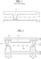
- FIG. 1 is a cross sectional view illustrating a related art LCD device.
- the related art LCD device may include a lower substrate 10, an upper substrate 20, and a liquid crystal layer 30 between the lower and upper substrates 10 and 20.
- a thin film transistor and a pixel electrode. Also, a lower alignment film 15 is formed on the uppermost surface of the lower substrate 10.
- the upper substrate 20 there is a color filter. Also, a column spacer 22 for maintaining a cell gap is formed on the upper substrate 20, and an upper alignment film 25 is formed on the uppermost surface of the upper substrate 20. An initial alignment of the liquid crystal layer 30 is controlled by the lower alignment film 15 and the upper alignment film 25.
- the related art LCD device may have the following disadvantages.
- the column spacer 22 is fixed to the upper substrate 20, however, the column spacer 22 is not fixed to the lower substrate 10. If an external force is applied to the related art LCD device, the column spacer 22 may be moved by the external force. Thus, the lower alignment film 15 formed on the lower substrate 10 may be damaged due to the column spacer 22 moved by the external force. If the lower alignment film 15 is damaged, the alignment of the liquid crystal layer 30 is not controlled so that problems such as brightness defects occur.
- US 2006/0290860 A1 , US 2010/0053536 A1 , US 2012/0138941 A1 and US 2013/0010238 A1 disclose examples of spacer configurations for maintaining a cell gap between substrates of an LCD device.
- Embodiments of the present invention are directed to a liquid crystal display device that substantially obviates one or more problems due to limitations and disadvantages of the related art.
- An aspect of the embodiments of the present invention is to provide a liquid crystal display device which helps to prevent a lower alignment film from being damaged by a column spacer.
- a liquid crystal display device that includes first and second substrates; a liquid crystal layer between the first and second substrates; first and second bumps on the first substrate; and at least one first protrusion facing the first bump, and at least one second protrusion facing the second bump, the first and second protrusions being on the second substrate, wherein the at least one first protrusion faces one side of the first bump, and the at least one second protrusion faces the other side of the second bump.
- the liquid crystal display device may further include gate and data lines on the first substrate, the gate line being in a first direction, and the data line being in a second direction, and wherein the first bump includes a first bar extending in a length direction of the gate line, the first bar being overlapped with the gate line, and the second bump includes a second bar extending in the length direction of the gate line, the second bar being overlapped with the gate line.
- the at least one first protrusion may be smaller in size than the first bump and may have a dot structure overlapped with the first bump
- the at least one second protrusion may be smaller in size than the second bump and may have a dot structure overlapped with the second bump.
- the first bump may further include a first extending portion extending from one side and from the other side of the first bar
- the second bump may further include a second extending portion extending from one side and from the other side of the second bar, wherein the at least one first protrusion is overlapped with the first extending portion extending from the one side of the first bar, and the at least one second protrusion is overlapped with the second extending portion extending from the other side of the second bar.
- the liquid crystal display device may further include a light-shielding layer being overlapped with the gate and data lines, a first extending light-shielding portion being overlapped with the first extending portion of the first bump, and a second extending light-shielding portion being overlapped with the second extending portion of the second bump, the light-shielding layer, the first extending light-shield portion and the second extending light-shield portion being on the second substrate.
- the first bump may further include a first extending portion extending from one side of the first bar, and a first groove is at the other side of the first bar
- the second bump may further include a second extending portion extending from the other side of the second bar, and a second groove is at one side of the second bar
- the at least one first protrusion may be overlapped with the first extending portion extending from the one side of the first bump
- the at least one second protrusion may be overlapped with the second extending portion extending from the other side of the second bump.
- the first and second protrusions may include a bar structure extending in a length direction of the data line, the first and second protrusions being overlapped with the data line, one portion of the at least one first protrusion may be overlapped with the first extending portion, and another portion of the at least one first protrusion may be not overlapped with the first extending portion, and one portion of the at least one second protrusion may be overlapped with the second extending portion, and another portion of the at least one second protrusion may be not overlapped with the second extending portion.
- the liquid crystal display device may further include a light-shielding layer being overlapped with the gate and data lines, a first extending light-shielding portion being overlapped with the first extending portion of the first bump, and a second extending light-shielding portion being overlapped with the second extending portion of the second bump, the light-shielding layer, the first extending light-shield portion and the second extending light-shield portion being on the second substrate.
- the first and second protrusions may include a bar structure extending in a length direction of the data line, the first and second protrusions being overlapped with the data line, and one portion of the at least one first protrusion may be overlapped with one side of the first bump, and one portion of the at least one second protrusion may be overlapped with the other side of the second bump.
- first bump and the second bump may be connected with each other by a connection portion.
- first bump and the at least one first protrusion may maintain a cell gap of the liquid crystal layer
- second bump and the at least one second protrusion may maintain the cell gap of the liquid crystal layer
- one side of the first bump and the other side of the second bump may be in combination with one among a combination of the left side with respect to the center of the first bump and the right side with respect to the center of the second bump, a combination of the right side with respect to the center of the first bump and the left side with respect to the center of the second bump, a combination of the upper side with respect to the center of the first bump and the lower side with respect to the center of the second bump, a combination of the lower side with respect to the center of the first bump and the upper side with respect to the center of the second bump, a combination of the lower left side with respect to the center of the first bump and the upper right side with respect to the center of the second bump, a combination of the upper left side with respect to the center of the first bump and the lower right side with respect to the center of the second bump, a combination of the lower right side with respect to the center of the first bump and the upper left side with respect to the center of the second bump, or a combination of the upper right side with respect to the center of the
- the liquid crystal display device may further include an alignment film on at least one among the first and second substrates, wherein the first and second bumps and the at least one first protrusion and the at least one second protrusion maintain a cell gap between the first and second substrates and reduce a damage of the alignment film even when the first and second bumps and/or the at least one first protrusion and the at least one second protrusion are affected by an external force.
- the first and second bumps and the at least one first protrusion and the at least one second protrusion may be configured such that the at least one second protrusion is maintained on the second bump if the at least one first protrusion is dislodged from the first bump by the external force.
- a liquid crystal display device may include a liquid crystal layer between first and second substrates; a structure fixed to each of the first and second substrates, the structure being between the first and second substrates; and an alignment film on at least one among the first and second substrates, wherein the structure maintains a cell gap between the first and second substrates and reduces a damage of the alignment film even when the structure is affected by an external force.
- the structure may include a first structure and a second structure, the first structure and the second structure being different from each other.
- the first structure may include a first bump fixed to the first substrate, and a first protrusion fixed to the second substrate
- the second structure may include a second bump fixed to the first substrate, and a second protrusion fixed to the second substrate.
- the first and second structures may be configured such that the second protrusion may be maintained on the second bump if the first protrusion is dislodged from the first bump by the external force.
- a liquid crystal display device may include a liquid crystal layer between first and second substrates; a first structure on the first substrate; a second structure on the second substrate, wherein the second structure faces the first structure; and an alignment film on at least one among the first and second substrates, wherein the first structure is configured to maintain a cell gap between the first and second substrates and reduces a damage of the alignment film if the second structure is affected by an external force.
- the first structure may have a bump shape
- the second structure may have a protrusion shape
- a width of the second structure may be smaller than a width of the first structure.
- the first structure and the second structure may be configured to maintain the cell gap of the liquid crystal layer.
- the first substrate may further include gate and data lines, the gate line being in a first direction, and the data line being in a second direction, and wherein the first structure includes at least one bar extending in a length direction of the gate line, the first structure being overlapped with the gate line.
- the second structure may be smaller in size than the first structure and has a dot structure overlapped with the first structure.
- the second structure may further include an extending portion extending from one side and from the other side of at least one bar, and a groove is at the other side of at least one bar.
- the second structure may include a bar structure extending in a length direction of the data line, the second structure being overlapped with the data line.
- a structure for example, an electrode, a line, a wiring, a layer, or a contact
- this description should be construed as including a case where the structures contact each other and moreover, a case where a third structure is disposed therebetween.
- first, second, etc. may be used herein to describe various elements, these elements should not be limited by these terms. These terms are only used to distinguish one element from another. For example, a first element could be termed a second element, and, similarly, a second element could be termed a first element, without departing from the scope of the present invention.
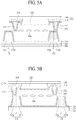
- FIG. 2 is a cross sectional view illustrating a liquid crystal display device according to one example embodiment of the present invention.
- the liquid crystal display device may include a first substrate 100, a second substrate 200, and a liquid crystal layer 300 between the first and second substrates 100 and 200.
- first substrate 100 On the first substrate 100, there is an element layer 110, bumps 131 and 132, and a first alignment film 150.
- the element layer 110 is formed on the first substrate 100.
- the element layer 110 may include gate and data lines crossing each other to define a pixel region, a thin film transistor connected with the gate and data lines, a pixel electrode connected with the thin film transistor, and a common electrode for controlling an alignment direction of the liquid crystal layer 300 by forming an electric field together with the pixel electrode. And the pixel region and another pixel region being adjacent to the pixel region may share one gate line or one date line.
- the element layer 110 may vary in structure.
- the liquid crystal display device according to the present invention may have various modes generally known to those in the art, for example, TN (Twisted Nematic), VA (Vertical Alignment), IPS (Inplane switching) or FFS (Fringe Field Switching) mode.
- TN and VA modes the common electrode is provided on the second substrate 200, whereby a vertical electric field is formed between the pixel electrode and the common electrode.
- the pixel electrode and the common electrode are provided on the first substrate 100, whereby a horizontal electric field is formed between the pixel electrode and the common electrode.
- each of the pixel and common electrodes may be changed to various shapes generally known to those in the art.
- the bumps 131 and 132 are formed on the element layer 110.
- the bumps 131 and 132 together with protrusions 231 and 232 to be explained later may maintain a cell gap of the liquid crystal display device. That is, a column spacer is formed by combination of the bumps 131 and 132 and the protrusions 231 and 232. This will be described later in detail.
- a height of each of the bumps 131 and 132, and the protrusions 231 and 232 should be determined in consideration of the cell gap of the liquid crystal display device.
- the height of the bumps 131 and 132 may be the same as the height of the protrusions 231 and 232, or may be different from the height of the protrusions 231 and 232.
- the height of each of the bumps 131 and 132 may be within a range of 0.5 ⁇ m to 2.0 ⁇ m, and the height of each of the protrusions 231 and 232 may be within a range of 0.5 ⁇ m to 2.0 ⁇ m.
- the first alignment film 150 is formed on the uppermost surface of the first substrate 100. Accordingly, the first alignment film 150 is formed on an upper surface of the bumps 131 and 132.
- the first alignment film 150 may be formed by aligning a polymer material such as polyimide in a predetermined direction using roller or ultraviolet rays (UV).
- a light-shielding layer 210, a color filter layer 220, the protrusions 231 and 232, and a second alignment film 250 are formed on the second substrate 200.
- the light-shielding layer 210 is provided in a matrix configuration on the second substrate 200.
- the light-shielding layer 210 prevents a light leakage in other regions except the pixel region.
- the color filter layer 220 is formed in a region between each pattern of the light-shielding layer 210 provided in the matrix configuration, that is, the pixel region.
- the color filter layer 220 may include red (R), green (G), and blue (B) color filters formed in the respective pixels.
- the protrusions 231 and 232 are formed on the light-shielding layer 210.
- the protrusions 231 and 232 are disposed to correspond with the bumps 131 and 132.
- the protrusions 231 and 232 and the bumps 131 and 132 are overlapped with the light-shielding layer 210 so that it is possible to prevent a light leakage in the regions of forming the respective protrusions 231 and 232 and the bumps 131 and 132.
- the second alignment film 250 is formed on the lowermost surface of the second substrate 200. Accordingly, the second alignment film 250 is formed on a lower surface of the protrusions 231 and 232.
- the second alignment film 250 may be formed by aligning a polymer material such as polyimide in a predetermined direction using roller or ultraviolet rays (UV).
- the alignment direction of the second alignment film 250 may be perpendicular to the alignment direction of the first alignment film 150, but is not necessarily.
- the bumps 131 and 132 are formed on the first substrate 100
- the protrusions 231 and 232 are formed on the second substrate 200
- the bumps 131 and 132 and the protrusions 231 and 232 face each other with the first and second alignment films 150 and 250 positioned in-between so that it is possible to maintain the cell gap of the liquid crystal display device by combination of the bumps 131 and 132 and the protrusions 231 and 232.
- the bumps 131 and 132 and the protrusions 231 and 232 may be formed of an organic polymer material such as acryl-based polymer, but is not limited to this material.
- the bumps 131 and 132 may be formed of the same material as that of a planarization film or passivation film for protecting the thin film transistor (T).
- the bumps 131 and 132 may be formed of an organic material such as acryl-based polymer, but is not limited to this material.
- the protrusions 231 and 232 on the second substrate 200 may be affected by the external force.
- a height of each of the protrusions 231 and 232 is lower than the cell gap, there is a low possibility that the first alignment film 150 on the first substrate 100 is damaged by the protrusions 231 and 232.
- a height of each of the protrusions 231 and 232 may be within a range of 0.5 ⁇ m to 2.0 ⁇ m.
- the bumps 131 and 132 and the protrusions 231 and 232 may be overlapped with the gate and data lines.
- the bumps 131 and 132 and the protrusions 231 and 232 may be overlapped with the gate and data lines.
- the bumps 131 and 132 include the first and second bumps 131 and 132, and the protrusions 231 and 232 include the first and second protrusions 231 and 232.
- the first bump 131 and the first protrusion 231 facing each other are provided to correspond with each other, and the second bump 132 and the second protrusion 232 facing each other are provided to correspond with each other.
- a width of the first protrusion 231 is smaller than a width of the first bump 131, whereby the overlapping area between the first bump 131 and the first protrusion 231 is decreased in size.
- a width of the second protrusion 232 is smaller than a width of the second bump 132, whereby the overlapping area between the second bump 132 and the second protrusion 232 is decreased in size.
- a facing position between the first bump 131 and the first protrusion 231 is different from a facing position between the second bump 132 and the second protrusion 232.
- the first bump 131 may include one side 131a and the other side 131b with respect to the center (c)
- the second bump 132 may include one side 132a and the other side 132b with respect to the center (c).
- one side 131a of the first bump 131 and one side 132a of the second bump 132 are disposed at the same side with respect to the center (c) of each bump
- the other side 131b of the first bump 131 and the other side 132b of the second bump 132 are disposed at the same side with respect to the center (c) of each bump
- each of one side of the first and second bumps 131 and 132 is opposite to each of the other side of the first and second bumps 131 and 132.
- the first protrusion 231 is disposed to face one side 131a of the first bump 131
- the second protrusion 232 is disposed to face the other side 132b of the second bump 132. That is, the first protrusion 231 and the second protrusion 232 are disposed at the different sides with respect to each of the first bump 131 and the second bump 132.
- the other among the protrusions 231 and 232 may be maintained on the other among the bumps 131 and 132.
- there is a low possibility that the first alignment film 150 is damaged by the protrusion 231 and 232 dislodged from the bump 131 and 132.
- FIGS. 3A and 3B are cross sectional views showing the protrusions 231 and 232 provided on the second substrate 200, which move by the external force, in the liquid crystal display device according to one example embodiment of the present invention.
- the first protrusion 231 and the second protrusion 232 moves toward the right direction.
- the first protrusion 231 disposed at one side 131a of the first bump 131 is maintained on the first bump 131 without being dislodged from the first bump 131.
- the first protrusion 231 and the second protrusion 232 moves toward the left direction.
- the first protrusion 231 disposed at one side 131a of the first bump 131 is dislodged from the first bump 131
- the second protrusion 232 disposed at the other side 132b of the second bump 132 is maintained on the second bump 132 without being dislodged from the second bump 132.
- FIG. 4 is a cross sectional view illustrating a liquid crystal display device according to another example embodiment of the present invention. Except a change in position of the first protrusion 231 and second protrusion 232, the liquid crystal display device of FIG. 4 is identical in structure to the liquid crystal display device of FIG. 2 , whereby the same reference numbers will be used throughout the drawings to refer to the same or like parts, and only different parts will be described in detail.
- the first protrusion 231 is disposed at the other side 131b of the first bump 131
- the second protrusion 232 is disposed at one side 132a of the second bump 132. Accordingly, even though any one among the protrusions 231 and 232 is dislodged from any one among the bumps 131 and 132, the other among the protrusions 231 and 232 may be maintained on the other among the bumps 131 and 132, to thereby prevent the first alignment film 150 from being damaged by the protrusions 231 and 232.
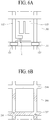
- FIGS. 5A and 5B are cross sectional views showing the protrusions 231 and 232 on the second substrate 200, which move by the external force, in the liquid crystal display device according to another example embodiment of the present invention.
- the first protrusion 231 disposed at the other side 131b of the first bump 131 is dislodged from the first bump 131, however, the second bump 232 disposed at one side 132a of the second bump 132 is not dislodged from the second bump 132, to thereby prevent the first alignment film 150 from being damaged by the first protrusion 231 dislodged from the first bump 131.
- the second protrusion 232 disposed at one side 132a of the second bump 132 is dislodged from the second bump 132, however, the first protrusion 231 disposed at the other side 131b of the first bum 131 is not dislodged from the first bump 131, to thereby prevent the first alignment film 150 from being damaged by the second protrusion 232 dislodged from the second bump 132.
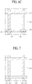
- FIG. 6A is a plane view illustrating the first substrate 100 of the liquid crystal display device according to one example embodiment of the present invention
- FIG. 6B is a plane view illustrating the second substrate 200 of the liquid crystal display device according to one example embodiment of the present invention
- FIG. 6C is a plane view illustrating a figure of overlap between the protrusions 231 and 232 and the bumps 131 and 132 in the liquid crystal display device according to one example embodiment of the present invention.
- the gate line 111 is disposed in a first direction on the first substrate 100
- the data line 112 is disposed in a second direction on the first substrate 100, to thereby define the pixel region by the gate and data lines 111 and 112 crossing each other, but is not limited thereto.
- the pixel region and another pixel region being adjacent to the pixel region may share one gate line or one date line.
- the thin film transistor (T) is formed at the crossing region of the gate and data lines 111 and 112, and the pixel electrode 113 being connected with the thin film transistor (T) is formed in the pixel region.
- the common electrode may be additionally formed on the first substrate 100, wherein the common electrode together with the pixel electrode 113 may form the electric field.
- first bump 131 and the second bump 132 are formed on the first substrate 100.
- the first bump 131 and the second bump 132 overlap with the gate line 111.
- each of the first bump 131 and the second bump 132 may include a bar structure extending in a length direction of the gate line 111.
- the light-shielding layer 210 of the matrix configuration is formed on the second substrate 200.
- the light-shielding layer 210 of the matrix configuration on the second substrate 200 is provided in correspondence with the gate and data lines 111 and 112 formed on the first substrate 100.
- first protrusion 231 and the second protrusion 232 are formed on the second substrate 200.
- the first protrusion 231 and the second protrusion 232 are overlapped with the light-shielding layer 210.
- the first protrusion 231 and the second protrusion 232 may include a dot structure overlapped with the light-shielding layer 210.
- the first protrusion 231 is positioned at an upper side as compared with the second protrusion 232
- the second protrusion 232 is positioned at a lower side as compared with the first protrusion 231.
- the first protrusion 231 may correspond to the first bump 131
- the second protrusion 232 may correspond to the second bump 132.
- FIG. 6B shows one among the first protrusion 231 and one among the second protrusion 232, but is not necessarily.
- Two or more first protrusions 231 may correspond to the first bump 131
- two or more second protrusions 232 may correspond to the second bump 132.
- the first bump 131, the second bump 132, the first protrusion 231, and the second protrusion 232 may be overlapped with the light-shielding layer 210, to thereby prevent a light leakage in the respective regions.
- the first protrusion 231 is overlapped with the first bump 131, and the second protrusion 232 is overlapped with the second bump 132.
- a size of the first protrusion 231 is smaller than a size of the first bump 131, and the entire first protrusion 231 is overlapped with the first bump 131.
- a size of the second protrusion 232 is smaller than a size of the second bump 132, and the entire second protrusion 232 is overlapped with the second bump 132.
- the first protrusion 231 may correspond to one side of the first bump 131, for example, the upper side of the first bump 131
- the second protrusion 232 may correspond to the other side of the second bump 132, for example, the lower side of the second bump 132.
- the first protrusion 231 is positioned at the upper side with respect to the center of the first bump 131, and the second protrusion 232 is positioned at the lower side with respect to the center of the second bump 232, but is not necessarily.
- the first protrusion 231 may be positioned at the lower side with respect to the center of the first bump 131, and the second protrusion 232 may be positioned at the upper side with respect to the center of the second bump 132.
- first protrusion 231 may be positioned at the left side with respect to the center of the first bump 131, and the second protrusion 232 may be positioned at the right side with respect to the center of the second bump 132.
- the first protrusion 231 may be positioned at the right side with respect to the center of the first bump 131, and the second protrusion 232 may be positioned at the left side with respect to the center of the second bump 132.
- first protrusion 231 and the second protrusion 232 may be positioned diagonal to the second protrusion 232. That is, the first protrusion 231 may be positioned at the lower left side with respect to the center of the first bump 131 and the second protrusion 232 may be positioned at the upper right side with respect to the center of the second bump 132; the first protrusion 231 may be positioned at the upper left side with respect to the center of the first bump 131 and the second protrusion 232 may be positioned at the lower right side with respect to the center of the second bump 132; the first protrusion 231 may be positioned at the lower right side with respect to the center of the first bump 131 and the second protrusion 232 may be positioned at the upper left side with respect to the center of the second bump 132; or the first protrusion 231 may be positioned at the upper right side with respect to the center of the first bump 131 and the second protrusion 232 may be positioned at the lower left side with respect to the center of the second bump
- first and second protrusions 231 and 232 may be applied to the various embodiments of the present invention to be explained as follows.
- FIG. 7 is a plane view illustrating the liquid crystal display device according to another example embodiment of the present invention, which shows that the protrusions 231 and 232 and the bumps 131 and 132 are overlapped as shown in FIG. 6C .
- the liquid crystal display device shown in FIG. 7 is identical in structure to the liquid crystal display device shown in FIGS. 6A to 6C .
- the first bump 131, the connection portion 133 and the second bump 132 may be connected as one body, and the one body structure of the first bump 131, the connection portion 133 and the second bump 132 may extend along the gate line 111.
- the gate line 111 may be connected as one body, and the one body structure of the first bump 131, the connection portion 133 and the second bump 132 may extend along the gate line 111.
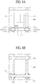
- FIG. 8A is a plane view illustrating a first substrate 100 of a liquid crystal display device according to another example embodiment of the present invention
- FIG. 8B is a plane view illustrating a second substrate 200 of the liquid crystal display device according to another example embodiment of the present invention
- FIG. 8C is a plane view illustrating a figure of overlap between protrusions 231 and 232 and bumps 131 and 132 in the liquid crystal display device according to another example embodiment of the present invention.
- a first bump 131 and a second bump 132 are formed on a first substrate 100.
- the first bump 131 may include a first bar 1311 extending in a length direction of the gate line 111, and a first extending portion 1312 extending from one side and the other side of the first bar 1311.
- the first bar 1311 is overlapped with the gate line 111, and the first extending portion 1312 may extend out of the gate line 111.
- the second bump 132 may include a second bar 1321 extending in a length direction of the gate line 111, and a second extending portion 1322 extending from one side and the other side of the second bar 1321.
- the second bar 1321 is overlapped with the gate line 111, and the second extending portion 1322 may extend out of the gate line 111.
- a light-shielding layer 210 having a matrix configuration is formed on a second substrate 200.
- a first extending light-shielding portion 211 and a second extending light-shielding portion 212 are connected with the light-shielding layer 210.
- the first extending light-shielding portion 211 is provided in correspondence with the first extending portion 1312 of the first bump 131, to thereby prevent a light leakage in the first extending portion 1312 of the first bump 131.
- the second extending light-shielding portion 212 is provided in correspondence with the second extending portion 1322 of the second bump 132, to thereby prevent a light leakage in the second extending portion 1322 of the second bump 132.
- the first bump 131, the second bump 132, the first protrusion 231 and the second protrusion 232 are overlapped with the light-shielding layer 210, the first extending light-shielding portion 211 and the second extending light-shielding portion 212, to thereby prevent a light leakage in the respective regions.
- the first protrusion 231 is overlapped with one side of the first bump 131, and more particularly, the first extending portion 1312 extending from one side of the first bar 1311.
- the second protrusion 232 is overlapped with the other side of the second bump 132, and more particularly, the second extending portion 1322 extending from the other side of the second bar 1321.
- the first bump 131 includes the first extending portion 1312
- the second bump 132 includes the second extending portion 1322, whereby the area of each of the first bump 131 and the second bump 132 is relatively increased as compared with the example embodiment shown in FIG. 6 . Accordingly, when the first protrusion 231 and the second protrusion 232 are moved by the external force, there is a high possibility that the first protrusion 231 and the second protrusion 232 are maintained on the first bump 131 and the second bump 132 without being dislodged from the first bump 131 and the second bump 132.
- FIG. 9 is a plane view illustrating the liquid crystal display device according to another example embodiment of the present invention, which shows that that the protrusions 231 and 232 and the bumps 131 and 132 are overlapped as shown in FIG. 8C .
- the liquid crystal display device shown in FIG. 9 is identical in structure to the liquid crystal display device shown in FIGS. 8A to 8C .
- the first bump 131, the connection portion 133 and the second bump 132 are formed as one body, the one body structure of the first bump 131, the connection portion 133 and the second bump 132 may extend along the gate line 111.
- FIG. 10A is a plane view illustrating a first substrate 100 of a liquid crystal display device according to another example embodiment of the present invention
- FIG. 10B is a plane view illustrating a second substrate 200 of the liquid crystal display device according to another example embodiment of the present invention
- FIG. 10C is a plane view illustrating a figure of overlap between protrusions 231 and 232 and bumps 131 and 132 in the liquid crystal display device according to another example embodiment of the present invention.
- the liquid crystal display device shown in FIGS. 10A to 10C is identical in structure to the liquid crystal display device shown in FIGS. 8A to 8C .
- the first extending portion 1312 and the second extending portion 1322 are formed in a polygonal shape, whereby the first extending light-shielding portion 211 and the second extending light-shielding portion 212 are formed in a polygonal shape in accordance with the first extending portion 1312 and the second extending portion 1322.
- the first extending portion 1312 and the second extending portion 1322 are formed in a curved-line shape such as semi-circle or semi-elliptical shape, whereby the first extending light-shielding portion 211 and the second extending light-shielding portion 212 are formed in a curved-line shape such as semi-circle or semi-elliptical shape.
- FIG. 11 is a plane view illustrating a liquid crystal display device according to another example embodiment of the present invention. Except that first and second bumps 131 and 132 are connected with each other by a connection portion 133, the liquid crystal display device shown in FIG. 11 is identical in structure to the liquid crystal display device shown in FIGS. 10A to 10C . Thus, in case of FIG. 11 , the first bump 131, the connection portion 133 and the second bump 132 may be connected as one body, and the one body structure of the first bump 131, the connection portion 133 and the second bump 132 may extend along the gate line 111.
- FIG. 12A is a plane view illustrating a first substrate 100 of a liquid crystal display device according to another example embodiment of the present invention
- FIG. 12B is a plane view illustrating a second substrate 200 of the liquid crystal display device according to another example embodiment of the present invention
- FIG. 12C is a plane view illustrating a figure of overlap between protrusions 231 and 232 and bumps 131 and 132 in the liquid crystal display device according to another example embodiment of the present invention.
- a first bump 131 and a second bump 132 are formed on a first substrate 100.
- the first bump 131 may include a first bar 1311 extending in a length direction of the gate line 111, and a first extending portion 1312 extending from one side of the first bar 1311.
- the first extending portion 1312 is formed in a curved-line shape such as semi-circle or semi-elliptical shape.
- a first groove 1311a is formed at the other side of the first bar 1311, wherein the first groove 1311a has a shape corresponding to the shape of the first extending portion 1312. However, the shape of the first groove 1311a may be different from the shape of the first extending portion 1312.
- the second bump 132 may include a second bar 1321 extending in the length direction of the gate line 111, and a second extending portion 1322 extending from the other side of the second bar 1321.
- the second extending portion 1322 is formed in a curved-line shape such as semi-circle or semi-elliptical shape.
- a second groove 1321a is formed at one side of the second bar 1321, wherein the second groove 1321a has a shape corresponding to the shape of the second extending portion 1322.
- the shape of the second groove 1321a may be different from the shape of the second extending portion 1322.
- a light-shielding layer 210 of a matrix configuration is formed on a second substrate 200.
- a first extending light-shielding portion 211 and a second extending light-shielding portion 212 are connected with the light-shielding layer 210.
- the first extending light-shielding portion 211 is provided in correspondence with the first extending portion 1312 of the first bump 131
- the second extending light-shielding portion 212 is provided in correspondence with the second extending portion 1322 of the second bump 132.
- a first protrusion 231 and a second protrusion 232 are formed on the second substrate 200, wherein each of the first protrusion 231 and the second protrusion 232 is formed in a bar shape overlapped with the light-shielding layer 210.
- the bar-shaped first protrusion 231 and second protrusion 232 extends in a length direction of the data line 112 while being overlapped with the data line 112 of the first substrate 110.
- the first bump 131, the second bump 132, the first protrusion 231 and the second protrusion 232 are overlapped with the light-shielding layer 210, the first extending light-shielding portion 211 and the second extending light-shielding portion 212.
- One portion of the first protrusion 231 is overlapped with one side of the first bump 131, and more particularly, the first extending portion 1312 extending from one side of the first bar 1311, and another portion of the first protrusion 231 is not overlapped with the first bump 131.
- another portion of the first protrusion 231 extends via the first groove 1311a provided in the first bar 1311 of the first bump 131.
- One portion of the second protrusion 232 is overlapped with the other side of the second bump 132, and more particularly, the second extending portion 1322 extending from the other side of the second bar 1321, and another portion of the second protrusion 232 is not overlapped with the second bump 132.
- another portion of the second protrusion 232 extends via the second groove 1321a provided in the second bar 1321 of the second bump 132.
- FIG. 13A is a plane view illustrating a first substrate 100 of a liquid crystal display device according to another example embodiment of the present invention
- FIG. 13B is a plane view illustrating a second substrate 200 of the liquid crystal display device according to another example embodiment of the present invention
- FIG. 13C is a plane view illustrating a figure of overlap figure between protrusions 231 and 232 and bumps 131 and 132 in the liquid crystal display device according to another example embodiment of the present invention.
- the liquid crystal display device shown in FIGS. 13A to 13C is identical in structure to the liquid crystal display device shown in FIGS. 12A to 12C .
- the first extending portion 1312 and the second extending portion 1322 are formed in a curved-line shape such as semi-circle or semi-elliptical shape, and the first extending light-shielding portion 211 and the second extending light-shielding portion 212 are formed in a curved-line shape.
- the first extending portion 1312 and the second extending portion 1322 are formed in a polygonal shape, and the and the first extending light-shielding portion 211 and the second extending light-shielding portion 212 are formed in a polygonal shape.
- FIG. 14A is a plane view illustrating a first substrate 100 of a liquid crystal display device according to another example embodiment of the present invention
- FIG. 14B is a plane view illustrating a second substrate 200 of the liquid crystal display device according to another example embodiment of the present invention
- FIG. 14C is a plane view illustrating a figure of overlap between protrusions 231 and 232 and bumps 131 and 132 in the liquid crystal display device according to another example embodiment of the present invention.
- a first bump 131 having a bar structure and a second bump 132 having a bar structure are formed on a first substrate 100.
- a first protrusion 231 having a bar structure and a second protrusion 232 having a bar structure are formed on a second substrate 200.
- the first and second bumps 131 and 132 are overlapped with a gate line 111 on the first substrate 100, and the first and second protrusions 231 and 232 are overlapped with a data line 112 on the first substrate 100.
- one side of the first protrusion 231 is overlapped with the other side of the first bump 131, and the other side of the first protrusion is not overlapped with the first bump 131.
- one side of the second protrusion 232 is overlapped with one side of the second bump 132, and the other side of the second protrusion 232 is not overlapped with the second bump 132.
- the first bump 131 and the second bump 132 are connected with each other by the connection portion (See '133' of FIGS. 7 , 9 and 11 ), whereby the first bump 131, the connection portion 133 and the second bump 132 are connected as one body.
- the protrusion formed on the second substrate when the protrusion formed on the second substrate is moved by the external force, it is possible to prevent the alignment film formed on the first substrate from being damaged by the protrusion.
- the overlapping area between the bump and the protrusion is decreased in size so that the liquid crystal layer surrounding the protrusion is easily restored after disappearance of the external force.
Landscapes
- Physics & Mathematics (AREA)
- Nonlinear Science (AREA)
- Mathematical Physics (AREA)
- Chemical & Material Sciences (AREA)
- Crystallography & Structural Chemistry (AREA)
- General Physics & Mathematics (AREA)
- Optics & Photonics (AREA)
- Spectroscopy & Molecular Physics (AREA)
- Engineering & Computer Science (AREA)
- Microelectronics & Electronic Packaging (AREA)
- Devices For Indicating Variable Information By Combining Individual Elements (AREA)
- Liquid Crystal (AREA)
Abstract
Description
- This application is a divisional application of European patent application No.
15 178 762.9 10-2014-0124590 filed on September 18, 2014 - Embodiments of the present invention relate to a liquid crystal display device, and more particularly, to the embodiments relate to a column spacer for maintaining a cell gap of a liquid crystal display device.
- Owing to advantages such as good portability and low power consumption by low operating voltage, a liquid crystal display (LCD) device is widely used in various fields of notebook computer, monitor, spacecraft, aircraft, and etc.
- The LCD device includes a lower substrate with a thin film transistor formed thereon, an upper substrate with a color filter formed thereon, and a liquid crystal layer formed between the lower and upper substrates. Also, a column spacer , which is used to maintain a cell gap between the lower and upper substrates is formed between the lower and upper substrates.
- Hereinafter, a related art LCD device will be described with reference to the accompanying drawings.
-
FIG. 1 is a cross sectional view illustrating a related art LCD device. - As shown in
FIG. 1 , the related art LCD device may include alower substrate 10, an upper substrate 20, and aliquid crystal layer 30 between the lower andupper substrates 10 and 20. - Although not shown, on the
lower substrate 10, there is a thin film transistor and a pixel electrode. Also, alower alignment film 15 is formed on the uppermost surface of thelower substrate 10. - Although not shown, on the upper substrate 20, there is a color filter. Also, a column spacer 22 for maintaining a cell gap is formed on the upper substrate 20, and an
upper alignment film 25 is formed on the uppermost surface of the upper substrate 20. An initial alignment of theliquid crystal layer 30 is controlled by thelower alignment film 15 and theupper alignment film 25. - However, the related art LCD device may have the following disadvantages.
- The column spacer 22 is fixed to the upper substrate 20, however, the column spacer 22 is not fixed to the
lower substrate 10. If an external force is applied to the related art LCD device, the column spacer 22 may be moved by the external force. Thus, thelower alignment film 15 formed on thelower substrate 10 may be damaged due to the column spacer 22 moved by the external force. If thelower alignment film 15 is damaged, the alignment of theliquid crystal layer 30 is not controlled so that problems such as brightness defects occur. -
US 2006/0290860 A1 ,US 2010/0053536 A1 ,US 2012/0138941 A1 andUS 2013/0010238 A1 disclose examples of spacer configurations for maintaining a cell gap between substrates of an LCD device. - Embodiments of the present invention are directed to a liquid crystal display device that substantially obviates one or more problems due to limitations and disadvantages of the related art.
- An aspect of the embodiments of the present invention is to provide a liquid crystal display device which helps to prevent a lower alignment film from being damaged by a column spacer.
- Additional advantages and features of the invention will be set forth in part in the description which follows and in part will become apparent to those having ordinary skill in the art upon examination of the following or may be learned from practice of the invention. These and other advantages of the invention may be realized and attained by the structure particularly pointed out in the written description and claims hereof as well as the appended drawings.
- To achieve these and other advantages and in accordance with the purpose of the invention, as embodied and broadly described herein, there is provided a liquid crystal display device according to
claim 1. Further embodiments are described in the dependent claims. In an aspect of the present invention, there is provided a liquid crystal display device that includes first and second substrates; a liquid crystal layer between the first and second substrates; first and second bumps on the first substrate; and at least one first protrusion facing the first bump, and at least one second protrusion facing the second bump, the first and second protrusions being on the second substrate, wherein the at least one first protrusion faces one side of the first bump, and the at least one second protrusion faces the other side of the second bump. - In addition, the liquid crystal display device may further include gate and data lines on the first substrate, the gate line being in a first direction, and the data line being in a second direction, and wherein the first bump includes a first bar extending in a length direction of the gate line, the first bar being overlapped with the gate line, and the second bump includes a second bar extending in the length direction of the gate line, the second bar being overlapped with the gate line.
- The at least one first protrusion may be smaller in size than the first bump and may have a dot structure overlapped with the first bump, and the at least one second protrusion may be smaller in size than the second bump and may have a dot structure overlapped with the second bump.
- Also, the first bump may further include a first extending portion extending from one side and from the other side of the first bar, and the second bump may further include a second extending portion extending from one side and from the other side of the second bar, wherein the at least one first protrusion is overlapped with the first extending portion extending from the one side of the first bar, and the at least one second protrusion is overlapped with the second extending portion extending from the other side of the second bar.
- Furthermore, the liquid crystal display device may further include a light-shielding layer being overlapped with the gate and data lines, a first extending light-shielding portion being overlapped with the first extending portion of the first bump, and a second extending light-shielding portion being overlapped with the second extending portion of the second bump, the light-shielding layer, the first extending light-shield portion and the second extending light-shield portion being on the second substrate.
- The first bump may further include a first extending portion extending from one side of the first bar, and a first groove is at the other side of the first bar, the second bump may further include a second extending portion extending from the other side of the second bar, and a second groove is at one side of the second bar, and the at least one first protrusion may be overlapped with the first extending portion extending from the one side of the first bump, and the at least one second protrusion may be overlapped with the second extending portion extending from the other side of the second bump.
- Also, the first and second protrusions may include a bar structure extending in a length direction of the data line, the first and second protrusions being overlapped with the data line, one portion of the at least one first protrusion may be overlapped with the first extending portion, and another portion of the at least one first protrusion may be not overlapped with the first extending portion, and one portion of the at least one second protrusion may be overlapped with the second extending portion, and another portion of the at least one second protrusion may be not overlapped with the second extending portion.
- Furthermore, the liquid crystal display device may further include a light-shielding layer being overlapped with the gate and data lines, a first extending light-shielding portion being overlapped with the first extending portion of the first bump, and a second extending light-shielding portion being overlapped with the second extending portion of the second bump, the light-shielding layer, the first extending light-shield portion and the second extending light-shield portion being on the second substrate.
- The first and second protrusions may include a bar structure extending in a length direction of the data line, the first and second protrusions being overlapped with the data line, and one portion of the at least one first protrusion may be overlapped with one side of the first bump, and one portion of the at least one second protrusion may be overlapped with the other side of the second bump.
- Also, the first bump and the second bump may be connected with each other by a connection portion.
- Also, the first bump and the at least one first protrusion may maintain a cell gap of the liquid crystal layer, and the second bump and the at least one second protrusion may maintain the cell gap of the liquid crystal layer.
- Also, one side of the first bump and the other side of the second bump may be in combination with one among a combination of the left side with respect to the center of the first bump and the right side with respect to the center of the second bump, a combination of the right side with respect to the center of the first bump and the left side with respect to the center of the second bump, a combination of the upper side with respect to the center of the first bump and the lower side with respect to the center of the second bump, a combination of the lower side with respect to the center of the first bump and the upper side with respect to the center of the second bump, a combination of the lower left side with respect to the center of the first bump and the upper right side with respect to the center of the second bump, a combination of the upper left side with respect to the center of the first bump and the lower right side with respect to the center of the second bump, a combination of the lower right side with respect to the center of the first bump and the upper left side with respect to the center of the second bump, or a combination of the upper right side with respect to the center of the first bump and the lower left side with respect to the center of the second bump.
- The liquid crystal display device may further include an alignment film on at least one among the first and second substrates, wherein the first and second bumps and the at least one first protrusion and the at least one second protrusion maintain a cell gap between the first and second substrates and reduce a damage of the alignment film even when the first and second bumps and/or the at least one first protrusion and the at least one second protrusion are affected by an external force. Also, the first and second bumps and the at least one first protrusion and the at least one second protrusion may be configured such that the at least one second protrusion is maintained on the second bump if the at least one first protrusion is dislodged from the first bump by the external force.
- In another aspect of the present invention, there is provided a liquid crystal display device that may include a liquid crystal layer between first and second substrates; a structure fixed to each of the first and second substrates, the structure being between the first and second substrates; and an alignment film on at least one among the first and second substrates, wherein the structure maintains a cell gap between the first and second substrates and reduces a damage of the alignment film even when the structure is affected by an external force.
- The structure may include a first structure and a second structure, the first structure and the second structure being different from each other.
- The first structure may include a first bump fixed to the first substrate, and a first protrusion fixed to the second substrate, and the second structure may include a second bump fixed to the first substrate, and a second protrusion fixed to the second substrate.
- The first and second structures may be configured such that the second protrusion may be maintained on the second bump if the first protrusion is dislodged from the first bump by the external force.
- In another aspect of the present invention, there is provided a liquid crystal display device that may include a liquid crystal layer between first and second substrates; a first structure on the first substrate; a second structure on the second substrate, wherein the second structure faces the first structure; and an alignment film on at least one among the first and second substrates, wherein the first structure is configured to maintain a cell gap between the first and second substrates and reduces a damage of the alignment film if the second structure is affected by an external force.
- The first structure may have a bump shape, and the second structure may have a protrusion shape.
- Also, a width of the second structure may be smaller than a width of the first structure.
- The first structure and the second structure may be configured to maintain the cell gap of the liquid crystal layer.
- The first substrate may further include gate and data lines, the gate line being in a first direction, and the data line being in a second direction, and wherein the first structure includes at least one bar extending in a length direction of the gate line, the first structure being overlapped with the gate line.
- The second structure may be smaller in size than the first structure and has a dot structure overlapped with the first structure.
- The second structure may further include an extending portion extending from one side and from the other side of at least one bar, and a groove is at the other side of at least one bar.
- The second structure may include a bar structure extending in a length direction of the data line, the second structure being overlapped with the data line.
- It is to be understood that both the foregoing general description and the following detailed description of the present invention are exemplary and explanatory and are intended to provide further explanation of the invention as claimed.
- The accompanying drawings, which are included to provide a further understanding of the invention and are incorporated in and constitute a part of this application, illustrate embodiments of the invention and together with the description serve to explain the principle of the invention. In the drawings:
-
FIG. 1 is a cross sectional view illustrating a related art LCD device; -
FIG. 2 is a cross sectional view illustrating a liquid crystal display device according to one example embodiment of the present invention; -
FIGS. 3A and 3B are cross sectional views showing that protrusion provided on the second substrate is affected by an external force in case of the liquid crystal display device according to one example embodiment of the present invention; -
FIG. 4 is a cross sectional view illustrating a liquid crystal display device according to another example embodiment of the present invention. -
FIGS. 5A and 5B are cross sectional views showing that protrusion provided on the second substrate is affected by an external force in case of the liquid crystal display device according to another example embodiment of the present invention; -
FIG. 6A is a plane view illustrating a first substrate of the liquid crystal display device according to one embodiment of the present invention,FIG. 6B is a plane view illustrating a second substrate of the liquid crystal display device according to one example embodiment of the present invention, andFIG. 6C is a plane view illustrating a figure of overlap between a protrusion and a bump in the liquid crystal display device according to one example embodiment of the present invention; -
FIG. 7 is a plane view illustrating a liquid crystal display device according to another example embodiment of the present invention; -
FIG. 8A is a plane view illustrating a first substrate of the liquid crystal display device according to another example embodiment of the present invention,FIG. 8B is a plane view illustrating a second substrate of the liquid crystal display device according to another example embodiment of the present invention, andFIG. 8C is a plane view illustrating a figure of overlap between a protrusion and a bump in the liquid crystal display device according to another example embodiment of the present invention; -
FIG. 9 is a plane view illustrating a liquid crystal display device according to another example embodiment of the present invention; -
FIG. 10A is a plane view illustrating a first substrate of the liquid crystal display device according to another example embodiment of the present invention,FIG. 10B is a plane view illustrating a second substrate of the liquid crystal display device according to another example embodiment of the present invention, andFIG. 10C is a plane view illustrating a figure of overlap between a protrusion and a bump in the liquid crystal display device according to another example embodiment of the present invention; -
FIG. 11 is a plane view illustrating a liquid crystal display device according to another example embodiment of the present invention; -
FIG. 12A is a plane view illustrating a first substrate of the liquid crystal display device according to another example embodiment of the present invention,FIG. 12B is a plane view illustrating a second substrate of the liquid crystal display device according to another example embodiment of the present invention, andFIG. 12C is a plane view illustrating a figure of overlap between a protrusion and a bump in the liquid crystal display device according to another example embodiment of the present invention; -
FIG. 13A is a plane view illustrating a first substrate of the liquid crystal display device according to another example embodiment of the present invention,FIG. 13B is a plane view illustrating a second substrate of the liquid crystal display device according to another example embodiment of the present invention, andFIG. 13C is a plane view illustrating a figure of overlap between a protrusion and a bump in the liquid crystal display device according to another example embodiment of the present invention; and -
FIG. 14A is a plane view illustrating a first substrate of the liquid crystal display device according to another example embodiment of the present invention,FIG. 14B is a plane view illustrating a second substrate of the liquid crystal display device according to another example embodiment of the present invention, andFIG. 14C is a plane view illustrating a figure of overlap between a protrusion and a bump in the liquid crystal display device according to another example embodiment of the present invention. - Reference will now be made in detail to the exemplary embodiments of the present invention, examples of which are illustrated in the accompanying drawings. Wherever possible, the same reference numbers will be used throughout the drawings to refer to the same or like parts.
- Advantages and features of the present invention, and implementation methods thereof will be clarified through following embodiments described with reference to the accompanying drawings. The present invention may, however, be embodied in different forms and should not be construed as limited to the embodiments set forth herein. Rather, these embodiments are provided so that this disclosure will be thorough and complete, and will fully convey the scope of the present invention to those skilled in the art. Further, the present invention is only defined by scopes of claims.
- A shape, a size, a ratio, an angle, and a number disclosed in the drawings for describing embodiments of the present invention are merely an example, and thus, the present invention is not limited to the illustrated details. Like reference numerals refer to like elements throughout. In the following description, when the detailed description of the relevant known function or configuration is determined to unnecessarily obscure the important point of the present invention, the detailed description will be omitted. In a case where 'comprise', 'have', and 'include' described in the present specification are used, another part may be added unless 'only∼' is used. The terms of a singular form may include plural forms unless referred to the contrary. In construing an element, the element is construed as including an error region although there is no explicit description.
- In description of embodiments of the present invention, when a structure (for example, an electrode, a line, a wiring, a layer, or a contact) is described as being formed at an upper portion/lower portion of another structure or on/under the other structure, this description should be construed as including a case where the structures contact each other and moreover, a case where a third structure is disposed therebetween.
- In describing a time relationship, for example, when the temporal order is described as 'after∼', 'subsequent∼', 'next∼', and 'before∼', a case which is not continuous may be included unless 'just' or 'direct' is used.
- It will be understood that, although the terms "first", "second", etc. may be used herein to describe various elements, these elements should not be limited by these terms. These terms are only used to distinguish one element from another. For example, a first element could be termed a second element, and, similarly, a second element could be termed a first element, without departing from the scope of the present invention.
- Features of various embodiments of the present invention may be partially or overall coupled to or combined with each other, and may be variously inter-operated with each other and driven technically as those skilled in the art can sufficiently understand. The embodiments of the present invention may be carried out independently from each other, or may be carried out together in co-dependent relationship.
- Hereinafter, embodiments of the present invention will be described with reference to the accompanying drawings.
-
FIG. 2 is a cross sectional view illustrating a liquid crystal display device according to one example embodiment of the present invention. - As shown in
FIG. 2 , the liquid crystal display device according to one example embodiment of the present invention may include afirst substrate 100, asecond substrate 200, and aliquid crystal layer 300 between the first andsecond substrates - On the
first substrate 100, there is anelement layer 110,bumps first alignment film 150. - The
element layer 110 is formed on thefirst substrate 100. Theelement layer 110 may include gate and data lines crossing each other to define a pixel region, a thin film transistor connected with the gate and data lines, a pixel electrode connected with the thin film transistor, and a common electrode for controlling an alignment direction of theliquid crystal layer 300 by forming an electric field together with the pixel electrode. And the pixel region and another pixel region being adjacent to the pixel region may share one gate line or one date line. - The
element layer 110 may vary in structure. For example, the liquid crystal display device according to the present invention may have various modes generally known to those in the art, for example, TN (Twisted Nematic), VA (Vertical Alignment), IPS (Inplane switching) or FFS (Fringe Field Switching) mode. In case of the TN and VA modes, the common electrode is provided on thesecond substrate 200, whereby a vertical electric field is formed between the pixel electrode and the common electrode. In case of the IPS and FFS modes, the pixel electrode and the common electrode are provided on thefirst substrate 100, whereby a horizontal electric field is formed between the pixel electrode and the common electrode. In each of the aforementioned modes, each of the pixel and common electrodes may be changed to various shapes generally known to those in the art. - The
bumps element layer 110. Thebumps protrusions bumps protrusions bumps protrusions bumps protrusions bumps protrusions protrusions bumps protrusions - The
first alignment film 150 is formed on the uppermost surface of thefirst substrate 100. Accordingly, thefirst alignment film 150 is formed on an upper surface of thebumps first alignment film 150 may be formed by aligning a polymer material such as polyimide in a predetermined direction using roller or ultraviolet rays (UV). - A light-
shielding layer 210, acolor filter layer 220, theprotrusions second alignment film 250 are formed on thesecond substrate 200. - The light-
shielding layer 210 is provided in a matrix configuration on thesecond substrate 200. The light-shielding layer 210 prevents a light leakage in other regions except the pixel region. - The
color filter layer 220 is formed in a region between each pattern of the light-shielding layer 210 provided in the matrix configuration, that is, the pixel region. Thecolor filter layer 220 may include red (R), green (G), and blue (B) color filters formed in the respective pixels. - The
protrusions shielding layer 210. Theprotrusions bumps protrusions bumps shielding layer 210 so that it is possible to prevent a light leakage in the regions of forming therespective protrusions bumps - The
second alignment film 250 is formed on the lowermost surface of thesecond substrate 200. Accordingly, thesecond alignment film 250 is formed on a lower surface of theprotrusions second alignment film 250 may be formed by aligning a polymer material such as polyimide in a predetermined direction using roller or ultraviolet rays (UV). The alignment direction of thesecond alignment film 250 may be perpendicular to the alignment direction of thefirst alignment film 150, but is not necessarily. - According to one example embodiment of the present invention, the
bumps first substrate 100, theprotrusions second substrate 200, and thebumps protrusions second alignment films bumps protrusions bumps protrusions bumps bumps - If an external force is applied to the liquid crystal display device according to one example embodiment of the present invention, the
protrusions second substrate 200 may be affected by the external force. However, since a height of each of theprotrusions first alignment film 150 on thefirst substrate 100 is damaged by theprotrusions protrusions - According to one example embodiment of the present invention, the
bumps protrusions bumps protrusions - If an overlapping area between the
bumps protrusions second alignment films second alignment films protrusions protrusions liquid crystal layer 300 around theprotrusions protrusions liquid crystal layer 300 around theprotrusions bumps protrusions bumps protrusions protrusions bumps first alignment film 150 may be damaged by theprotrusion - Accordingly, there has been a need to decrease the overlapping area between the
bumps protrusions protrusions bumps bumps protrusions - The
bumps second bumps protrusions second protrusions - The
first bump 131 and thefirst protrusion 231 facing each other are provided to correspond with each other, and thesecond bump 132 and thesecond protrusion 232 facing each other are provided to correspond with each other. - In this case, a width of the
first protrusion 231 is smaller than a width of thefirst bump 131, whereby the overlapping area between thefirst bump 131 and thefirst protrusion 231 is decreased in size. Also, a width of thesecond protrusion 232 is smaller than a width of thesecond bump 132, whereby the overlapping area between thesecond bump 132 and thesecond protrusion 232 is decreased in size. - Also, a facing position between the
first bump 131 and thefirst protrusion 231 is different from a facing position between thesecond bump 132 and thesecond protrusion 232. Thus, it is possible to reduce the problem caused by a case that theprotrusions bumps - In detail, the
first bump 131 may include oneside 131a and theother side 131b with respect to the center (c), and thesecond bump 132 may include oneside 132a and theother side 132b with respect to the center (c). In this specification of the present invention, oneside 131a of thefirst bump 131 and oneside 132a of thesecond bump 132 are disposed at the same side with respect to the center (c) of each bump, theother side 131b of thefirst bump 131 and theother side 132b of thesecond bump 132 are disposed at the same side with respect to the center (c) of each bump, and each of one side of the first andsecond bumps second bumps - According to one example embodiment of the present invention, the
first protrusion 231 is disposed to face oneside 131a of thefirst bump 131, and thesecond protrusion 232 is disposed to face theother side 132b of thesecond bump 132. That is, thefirst protrusion 231 and thesecond protrusion 232 are disposed at the different sides with respect to each of thefirst bump 131 and thesecond bump 132. Thus, if any one among theprotrusions bumps protrusions bumps first alignment film 150 is damaged by theprotrusion bump -
FIGS. 3A and 3B are cross sectional views showing theprotrusions second substrate 200, which move by the external force, in the liquid crystal display device according to one example embodiment of the present invention. - As shown in
FIG. 3A , if the external force is applied in the direction from the left side to the right side, thefirst protrusion 231 and thesecond protrusion 232 moves toward the right direction. In this case, while thesecond protrusion 232 disposed at theother side 132b of thesecond bump 132 is dislodged from thesecond bump 132, thefirst protrusion 231 disposed at oneside 131a of thefirst bump 131 is maintained on thefirst bump 131 without being dislodged from thefirst bump 131. Accordingly, it is possible to maintain the cell gap of the liquid crystal display device by the combination of thefirst bump 131 and thefirst protrusion 231, that is, it is possible to prevent thefirst alignment film 150 from being damaged by thesecond protrusion 232 dislodged from thesecond bump 132. - As shown in
FIG. 3B , if the external force is applied in the direction from the right side to the left side, thefirst protrusion 231 and thesecond protrusion 232 moves toward the left direction. In this case, while thefirst protrusion 231 disposed at oneside 131a of thefirst bump 131 is dislodged from thefirst bump 131, thesecond protrusion 232 disposed at theother side 132b of thesecond bump 132 is maintained on thesecond bump 132 without being dislodged from thesecond bump 132. Accordingly, it is possible to maintain the cell gap of the liquid crystal display device by the combination of thesecond bump 132 and thesecond protrusion 232, that is, it is possible to prevent thefirst alignment film 150 from being damaged by thefirst protrusion 231 dislodged from thefirst bump 131. -
FIG. 4 is a cross sectional view illustrating a liquid crystal display device according to another example embodiment of the present invention. Except a change in position of thefirst protrusion 231 andsecond protrusion 232, the liquid crystal display device ofFIG. 4 is identical in structure to the liquid crystal display device ofFIG. 2 , whereby the same reference numbers will be used throughout the drawings to refer to the same or like parts, and only different parts will be described in detail. - As shown in
FIG. 4 , according to another example embodiment of the present invention, thefirst protrusion 231 is disposed at theother side 131b of thefirst bump 131, and thesecond protrusion 232 is disposed at oneside 132a of thesecond bump 132. Accordingly, even though any one among theprotrusions bumps protrusions bumps first alignment film 150 from being damaged by theprotrusions -
FIGS. 5A and 5B are cross sectional views showing theprotrusions second substrate 200, which move by the external force, in the liquid crystal display device according to another example embodiment of the present invention. - As shown in
FIG. 5A , if the external force is applied in the direction from the left side to the right side, thefirst protrusion 231 disposed at theother side 131b of thefirst bump 131 is dislodged from thefirst bump 131, however, thesecond bump 232 disposed at oneside 132a of thesecond bump 132 is not dislodged from thesecond bump 132, to thereby prevent thefirst alignment film 150 from being damaged by thefirst protrusion 231 dislodged from thefirst bump 131. - As shown in
FIG. 5B , if the external force is applied in the direction from the right side to the left side, thesecond protrusion 232 disposed at oneside 132a of thesecond bump 132 is dislodged from thesecond bump 132, however, thefirst protrusion 231 disposed at theother side 131b of thefirst bum 131 is not dislodged from thefirst bump 131, to thereby prevent thefirst alignment film 150 from being damaged by thesecond protrusion 232 dislodged from thesecond bump 132. -
FIG. 6A is a plane view illustrating thefirst substrate 100 of the liquid crystal display device according to one example embodiment of the present invention,FIG. 6B is a plane view illustrating thesecond substrate 200 of the liquid crystal display device according to one example embodiment of the present invention, andFIG. 6C is a plane view illustrating a figure of overlap between theprotrusions bumps - As shown in
FIG. 6A , thegate line 111 is disposed in a first direction on thefirst substrate 100, and thedata line 112 is disposed in a second direction on thefirst substrate 100, to thereby define the pixel region by the gate anddata lines data lines pixel electrode 113 being connected with the thin film transistor (T) is formed in the pixel region. The common electrode may be additionally formed on thefirst substrate 100, wherein the common electrode together with thepixel electrode 113 may form the electric field. - Also, the
first bump 131 and thesecond bump 132 are formed on thefirst substrate 100. Thefirst bump 131 and thesecond bump 132 overlap with thegate line 111. In more detail, each of thefirst bump 131 and thesecond bump 132 may include a bar structure extending in a length direction of thegate line 111. - As shown in
FIG. 6B , the light-shielding layer 210 of the matrix configuration is formed on thesecond substrate 200. The light-shielding layer 210 of the matrix configuration on thesecond substrate 200 is provided in correspondence with the gate anddata lines first substrate 100. - Also, the
first protrusion 231 and thesecond protrusion 232 are formed on thesecond substrate 200. Thefirst protrusion 231 and thesecond protrusion 232 are overlapped with the light-shielding layer 210. In more detail, thefirst protrusion 231 and thesecond protrusion 232 may include a dot structure overlapped with the light-shielding layer 210. Especially, thefirst protrusion 231 is positioned at an upper side as compared with thesecond protrusion 232, and thesecond protrusion 232 is positioned at a lower side as compared with thefirst protrusion 231. - The
first protrusion 231 may correspond to thefirst bump 131, and thesecond protrusion 232 may correspond to thesecond bump 132.FIG. 6B shows one among thefirst protrusion 231 and one among thesecond protrusion 232, but is not necessarily. Two or morefirst protrusions 231 may correspond to thefirst bump 131, and two or moresecond protrusions 232 may correspond to thesecond bump 132. Also, it is possible to reverse the shape of the first andsecond protrusions second bumps - As shown in
FIG. 6C , thefirst bump 131, thesecond bump 132, thefirst protrusion 231, and thesecond protrusion 232 may be overlapped with the light-shielding layer 210, to thereby prevent a light leakage in the respective regions. - The
first protrusion 231 is overlapped with thefirst bump 131, and thesecond protrusion 232 is overlapped with thesecond bump 132. Especially, a size of thefirst protrusion 231 is smaller than a size of thefirst bump 131, and the entirefirst protrusion 231 is overlapped with thefirst bump 131. Also, a size of thesecond protrusion 232 is smaller than a size of thesecond bump 132, and the entiresecond protrusion 232 is overlapped with thesecond bump 132. - In this case, the
first protrusion 231 may correspond to one side of thefirst bump 131, for example, the upper side of thefirst bump 131, and thesecond protrusion 232 may correspond to the other side of thesecond bump 132, for example, the lower side of thesecond bump 132. Thus, as described above, even though any one among theprotrusions bumps protrusions bumps bumps - In
FIG. 6C , thefirst protrusion 231 is positioned at the upper side with respect to the center of thefirst bump 131, and thesecond protrusion 232 is positioned at the lower side with respect to the center of thesecond bump 232, but is not necessarily. Thefirst protrusion 231 may be positioned at the lower side with respect to the center of thefirst bump 131, and thesecond protrusion 232 may be positioned at the upper side with respect to the center of thesecond bump 132. - Also, the
first protrusion 231 may be positioned at the left side with respect to the center of thefirst bump 131, and thesecond protrusion 232 may be positioned at the right side with respect to the center of thesecond bump 132. Thefirst protrusion 231 may be positioned at the right side with respect to the center of thefirst bump 131, and thesecond protrusion 232 may be positioned at the left side with respect to the center of thesecond bump 132. - Also, the
first protrusion 231 and thesecond protrusion 232 may be positioned diagonal to thesecond protrusion 232. That is, thefirst protrusion 231 may be positioned at the lower left side with respect to the center of thefirst bump 131 and thesecond protrusion 232 may be positioned at the upper right side with respect to the center of thesecond bump 132; thefirst protrusion 231 may be positioned at the upper left side with respect to the center of thefirst bump 131 and thesecond protrusion 232 may be positioned at the lower right side with respect to the center of thesecond bump 132; thefirst protrusion 231 may be positioned at the lower right side with respect to the center of thefirst bump 131 and thesecond protrusion 232 may be positioned at the upper left side with respect to the center of thesecond bump 132; or thefirst protrusion 231 may be positioned at the upper right side with respect to the center of thefirst bump 131 and thesecond protrusion 232 may be positioned at the lower left side with respect to the center of thesecond bump 132 - The various positions of the first and
second protrusions -
FIG. 7 is a plane view illustrating the liquid crystal display device according to another example embodiment of the present invention, which shows that theprotrusions bumps FIG. 6C . - Except that the
first bump 131 and thesecond bump 132 are connected with each other by aconnection portion 133, the liquid crystal display device shown inFIG. 7 is identical in structure to the liquid crystal display device shown inFIGS. 6A to 6C . - As shown in
FIG. 7 , according to another example embodiment of the present invention, thefirst bump 131, theconnection portion 133 and thesecond bump 132 may be connected as one body, and the one body structure of thefirst bump 131, theconnection portion 133 and thesecond bump 132 may extend along thegate line 111. Hereinafter, only different structures, which are different from those ofFIGS. 6A to 6C , will be described in detail as follows. -
FIG. 8A is a plane view illustrating afirst substrate 100 of a liquid crystal display device according to another example embodiment of the present invention,FIG. 8B is a plane view illustrating asecond substrate 200 of the liquid crystal display device according to another example embodiment of the present invention, andFIG. 8C is a plane view illustrating a figure of overlap betweenprotrusions bumps - As shown in
FIG. 8A , afirst bump 131 and asecond bump 132 are formed on afirst substrate 100. - The
first bump 131 may include afirst bar 1311 extending in a length direction of thegate line 111, and a first extendingportion 1312 extending from one side and the other side of thefirst bar 1311. Thefirst bar 1311 is overlapped with thegate line 111, and the first extendingportion 1312 may extend out of thegate line 111. - The
second bump 132 may include asecond bar 1321 extending in a length direction of thegate line 111, and a second extendingportion 1322 extending from one side and the other side of thesecond bar 1321. Thesecond bar 1321 is overlapped with thegate line 111, and the second extendingportion 1322 may extend out of thegate line 111. - As shown in
FIG. 8B , a light-shielding layer 210 having a matrix configuration is formed on asecond substrate 200. A first extending light-shieldingportion 211 and a second extending light-shieldingportion 212 are connected with the light-shielding layer 210. The first extending light-shieldingportion 211 is provided in correspondence with the first extendingportion 1312 of thefirst bump 131, to thereby prevent a light leakage in the first extendingportion 1312 of thefirst bump 131. The second extending light-shieldingportion 212 is provided in correspondence with the second extendingportion 1322 of thesecond bump 132, to thereby prevent a light leakage in the second extendingportion 1322 of thesecond bump 132. - As shown in
FIG. 8C , thefirst bump 131, thesecond bump 132, thefirst protrusion 231 and thesecond protrusion 232 are overlapped with the light-shielding layer 210, the first extending light-shieldingportion 211 and the second extending light-shieldingportion 212, to thereby prevent a light leakage in the respective regions. - The
first protrusion 231 is overlapped with one side of thefirst bump 131, and more particularly, the first extendingportion 1312 extending from one side of thefirst bar 1311. Thesecond protrusion 232 is overlapped with the other side of thesecond bump 132, and more particularly, the second extendingportion 1322 extending from the other side of thesecond bar 1321. - In case of the example embodiment shown in
FIGS. 8A to 8C , thefirst bump 131 includes the first extendingportion 1312, and thesecond bump 132 includes the second extendingportion 1322, whereby the area of each of thefirst bump 131 and thesecond bump 132 is relatively increased as compared with the example embodiment shown inFIG. 6 . Accordingly, when thefirst protrusion 231 and thesecond protrusion 232 are moved by the external force, there is a high possibility that thefirst protrusion 231 and thesecond protrusion 232 are maintained on thefirst bump 131 and thesecond bump 132 without being dislodged from thefirst bump 131 and thesecond bump 132. -
FIG. 9 is a plane view illustrating the liquid crystal display device according to another example embodiment of the present invention, which shows that that theprotrusions bumps FIG. 8C . - Except that the
first bump 131 and thesecond bump 132 are connected with each other by aconnection portion 133, the liquid crystal display device shown inFIG. 9 is identical in structure to the liquid crystal display device shown inFIGS. 8A to 8C . In case ofFIG. 9 , thefirst bump 131, theconnection portion 133 and thesecond bump 132 are formed as one body, the one body structure of thefirst bump 131, theconnection portion 133 and thesecond bump 132 may extend along thegate line 111. -
FIG. 10A is a plane view illustrating afirst substrate 100 of a liquid crystal display device according to another example embodiment of the present invention,FIG. 10B is a plane view illustrating asecond substrate 200 of the liquid crystal display device according to another example embodiment of the present invention, andFIG. 10C is a plane view illustrating a figure of overlap betweenprotrusions bumps - Except that the first extending
portion 1312 of thefirst bump 131, the second extendingportion 1322 of thesecond bump 132, the first extending light-shieldingportion 211 and the second extending light-shieldingportion 212 are changed in shape, the liquid crystal display device shown inFIGS. 10A to 10C is identical in structure to the liquid crystal display device shown inFIGS. 8A to 8C . - In case of the liquid crystal display device shown in
FIGS. 8A to 8C , the first extendingportion 1312 and the second extendingportion 1322 are formed in a polygonal shape, whereby the first extending light-shieldingportion 211 and the second extending light-shieldingportion 212 are formed in a polygonal shape in accordance with the first extendingportion 1312 and the second extendingportion 1322. - Meanwhile, in case of the liquid crystal display device shown in
FIGS. 10A to 10C , the first extendingportion 1312 and the second extendingportion 1322 are formed in a curved-line shape such as semi-circle or semi-elliptical shape, whereby the first extending light-shieldingportion 211 and the second extending light-shieldingportion 212 are formed in a curved-line shape such as semi-circle or semi-elliptical shape. -
FIG. 11 is a plane view illustrating a liquid crystal display device according to another example embodiment of the present invention. Except that first andsecond bumps connection portion 133, the liquid crystal display device shown inFIG. 11 is identical in structure to the liquid crystal display device shown inFIGS. 10A to 10C . Thus, in case ofFIG. 11 , thefirst bump 131, theconnection portion 133 and thesecond bump 132 may be connected as one body, and the one body structure of thefirst bump 131, theconnection portion 133 and thesecond bump 132 may extend along thegate line 111. -
FIG. 12A is a plane view illustrating afirst substrate 100 of a liquid crystal display device according to another example embodiment of the present invention,FIG. 12B is a plane view illustrating asecond substrate 200 of the liquid crystal display device according to another example embodiment of the present invention, andFIG. 12C is a plane view illustrating a figure of overlap betweenprotrusions bumps - As shown in
FIG. 12A , afirst bump 131 and asecond bump 132 are formed on afirst substrate 100. - The
first bump 131 may include afirst bar 1311 extending in a length direction of thegate line 111, and a first extendingportion 1312 extending from one side of thefirst bar 1311. The first extendingportion 1312 is formed in a curved-line shape such as semi-circle or semi-elliptical shape. Afirst groove 1311a is formed at the other side of thefirst bar 1311, wherein thefirst groove 1311a has a shape corresponding to the shape of the first extendingportion 1312. However, the shape of thefirst groove 1311a may be different from the shape of the first extendingportion 1312. - The
second bump 132 may include asecond bar 1321 extending in the length direction of thegate line 111, and a second extendingportion 1322 extending from the other side of thesecond bar 1321. The second extendingportion 1322 is formed in a curved-line shape such as semi-circle or semi-elliptical shape. Asecond groove 1321a is formed at one side of thesecond bar 1321, wherein thesecond groove 1321a has a shape corresponding to the shape of the second extendingportion 1322. However, the shape of thesecond groove 1321a may be different from the shape of the second extendingportion 1322. - As shown in
FIG. 12B , a light-shielding layer 210 of a matrix configuration is formed on asecond substrate 200. A first extending light-shieldingportion 211 and a second extending light-shieldingportion 212 are connected with the light-shielding layer 210. The first extending light-shieldingportion 211 is provided in correspondence with the first extendingportion 1312 of thefirst bump 131, and the second extending light-shieldingportion 212 is provided in correspondence with the second extendingportion 1322 of thesecond bump 132. - A
first protrusion 231 and asecond protrusion 232 are formed on thesecond substrate 200, wherein each of thefirst protrusion 231 and thesecond protrusion 232 is formed in a bar shape overlapped with the light-shielding layer 210. The bar-shapedfirst protrusion 231 andsecond protrusion 232 extends in a length direction of thedata line 112 while being overlapped with thedata line 112 of thefirst substrate 110. - As shown in
FIG. 12C , thefirst bump 131, thesecond bump 132, thefirst protrusion 231 and thesecond protrusion 232 are overlapped with the light-shielding layer 210, the first extending light-shieldingportion 211 and the second extending light-shieldingportion 212. - One portion of the
first protrusion 231 is overlapped with one side of thefirst bump 131, and more particularly, the first extendingportion 1312 extending from one side of thefirst bar 1311, and another portion of thefirst protrusion 231 is not overlapped with thefirst bump 131. In more detail, another portion of thefirst protrusion 231 extends via thefirst groove 1311a provided in thefirst bar 1311 of thefirst bump 131. - One portion of the
second protrusion 232 is overlapped with the other side of thesecond bump 132, and more particularly, the second extendingportion 1322 extending from the other side of thesecond bar 1321, and another portion of thesecond protrusion 232 is not overlapped with thesecond bump 132. In more detail, another portion of thesecond protrusion 232 extends via thesecond groove 1321a provided in thesecond bar 1321 of thesecond bump 132. -
FIG. 13A is a plane view illustrating afirst substrate 100 of a liquid crystal display device according to another example embodiment of the present invention,FIG. 13B is a plane view illustrating asecond substrate 200 of the liquid crystal display device according to another example embodiment of the present invention, andFIG. 13C is a plane view illustrating a figure of overlap figure betweenprotrusions bumps - Except that the first extending
portion 1312 of thefirst bump 131, the second extendingportion 1322 of thesecond bump 132, the first extending light-shieldingportion 211 and the second extending light-shieldingportion 212 are changed in shape, the liquid crystal display device shown inFIGS. 13A to 13C is identical in structure to the liquid crystal display device shown inFIGS. 12A to 12C . - In case of the liquid crystal display device shown in
FIGS. 12A to 12C , the first extendingportion 1312 and the second extendingportion 1322 are formed in a curved-line shape such as semi-circle or semi-elliptical shape, and the first extending light-shieldingportion 211 and the second extending light-shieldingportion 212 are formed in a curved-line shape. - Meanwhile, in case of the liquid crystal display device shown in
FIGS. 13A to 13C , the first extendingportion 1312 and the second extendingportion 1322 are formed in a polygonal shape, and the and the first extending light-shieldingportion 211 and the second extending light-shieldingportion 212 are formed in a polygonal shape. -
FIG. 14A is a plane view illustrating afirst substrate 100 of a liquid crystal display device according to another example embodiment of the present invention,FIG. 14B is a plane view illustrating asecond substrate 200 of the liquid crystal display device according to another example embodiment of the present invention, andFIG. 14C is a plane view illustrating a figure of overlap betweenprotrusions bumps - As shown in
FIG. 14A , afirst bump 131 having a bar structure and asecond bump 132 having a bar structure are formed on afirst substrate 100. As shown inFIG. 14B , afirst protrusion 231 having a bar structure and asecond protrusion 232 having a bar structure are formed on asecond substrate 200. - The first and
second bumps gate line 111 on thefirst substrate 100, and the first andsecond protrusions data line 112 on thefirst substrate 100. - As shown in
FIG. 14C , one side of thefirst protrusion 231 is overlapped with the other side of thefirst bump 131, and the other side of the first protrusion is not overlapped with thefirst bump 131. Also, one side of thesecond protrusion 232 is overlapped with one side of thesecond bump 132, and the other side of thesecond protrusion 232 is not overlapped with thesecond bump 132. - Meanwhile, although not shown, in case of the liquid crystal display device shown in
FIGS. 12A to 12C ,FIGS. 13A to 13C andFIGS. 14A to 14C , thefirst bump 131 and thesecond bump 132 are connected with each other by the connection portion (See '133' ofFIGS. 7 ,9 and11 ), whereby thefirst bump 131, theconnection portion 133 and thesecond bump 132 are connected as one body. - According to the present invention, when the protrusion formed on the second substrate is moved by the external force, it is possible to prevent the alignment film formed on the first substrate from being damaged by the protrusion.
- Also, the overlapping area between the bump and the protrusion is decreased in size so that the liquid crystal layer surrounding the protrusion is easily restored after disappearance of the external force.
- It will be apparent to those skilled in the art that various modifications and variations can be made in the present invention within the scope of the claims.
Claims (12)
- A liquid crystal display device comprising:first and second substrates (100, 200);a liquid crystal layer (300) between the first and second substrates (100, 200);gate and data lines (111, 112) on the first substrate (100), the gate line (111) being in a first direction, and the data line (112) being in a second direction;first and second bumps (131, 132) on the first substrate (100); andat least one first protrusion (231) facing the first bump (131), and at least one second protrusion (232) facing the second bump (132), the first and second protrusions (231, 232) being on the second substrate (200),wherein the at least one first protrusion (231) faces one side of the first bump (131) with respect to the center (c) of the first bump (131), and the at least one second protrusion (232) faces an opposite side of the second bump (132) with respect to the center (c) of the second bump (132),wherein the first bump (131) includes- a first bar (1311) extending in a length direction of the gate line (111) and overlapping the gate line (111),- a first extending portion (1312) extending from one side of the first bar (1311) and extending out of the gate line (111), and- a first groove (1311a) provided at an opposite side of the first bar (1311),wherein the second bump (132) includes- a second bar (1321) extending in the length direction of the gate line (111) and overlapping the gate line (111),- a second extending portion (1322) extending from an opposite side of the second bar (1321) and extending out of the gate line (111), and- a second groove (1321a) provided at one side of the second bar (1321).
- The liquid crystal display device according to claim 1,
wherein the first and second protrusions (231, 232) include a bar structure extending in a length direction of the data line (112). - The liquid crystal display device according to claim 2,
wherein the bar structure overlaps the data line (112). - The liquid crystal display device according to claim 1,
wherein one portion of the at least one first protrusion (231) is overlapped with the first extending portion (1312), and another portion of the at least one first protrusion (231) is not overlapped with the first extending portion (1312), and
one portion of the at least one second protrusion (232) is overlapped with the second extending portion (1322), and another portion of the at least one second protrusion (232) is not overlapped with the second extending portion (1322). - The liquid crystal display device according to claim 4,
wherein the another portion of the at least one first protrusion (231) is overlapped with the first groove (1311a), and
the another portion of the at least one second protrusion (232) is overlapped with the second groove (1321a). - The liquid crystal display device according to any one of claims 1 to 5,
wherein the first extending portion and the second extending portion are formed in a curved-line shape. - The liquid crystal display device according to any one of claims 1 to 5,
wherein the first extending portion and the second extending portion are formed in a polygonal shape. - The liquid crystal display device according to any one of claims 1 to 7, further comprising a light-shielding layer (210) overlapping the gate and data lines (111, 112), a first extending light-shielding portion (211) overlapping the first extending portion (1312) of the first bump (131), and a second extending light-shielding portion (212) overlapping the second extending portion (1322) of the second bump (132), the light-shielding layer (210), the first extending light-shielding portion (211) and the second extending light-shielding portion (212) being on the second substrate (200).
- The liquid crystal display device according to any one of claims 1 to 7, further comprising a light-shielding layer (210) overlapping the gate and data lines (111, 112), the light-shielding layer (210) including a first extending light-shielding portion (211) and a second extending light-shielding portion (212),
wherein the first bump (131), the second bump (132), the at least one first protrusion (231) and the at least one second protrusion (232) are overlapped with the light-shielding layer (210), the first extending light-shielding portion (211), and the second extending light-shielding portion (212). - The liquid crystal display device according to any one of claims 1 to 9, further comprising:a first alignment film (150) on the first substrate (100) and a second alignment film (250) on the second substrate (200),wherein the first alignment film (150) is on the first and second bumps (131, 132), the second alignment film (250) is on the first and second protrusions (231, 232), andwherein the first bump (131) and the at least one first protrusion (231) maintain a cell gap of the liquid crystal layer (300), and the second bump (132) and the at least one second protrusion (232) maintain the cell gap of the liquid crystal layer (300).
- The liquid crystal display device according to any one of claims 1 to 10, wherein a first pair having the first bump (131) and the first protrusion (231) and a second pair having the second bump (132) and the second protrusion (232) are configured such that at least one among the first protrusion (231) and the second protrusion (232) is maintained on the first bump (131) or the second bump (132), respectively, even if the first protrusion (231) or the second protrusion (232) is dislodged from the first bump (131) or the second bump (132), respectively.
- The liquid crystal display device according to any one of claims 1 to 11, further comprising a pixel electrode (113) and a common electrode on the first substrate (100), wherein the pixel electrode (113) and the common electrode form an electric field.
Applications Claiming Priority (2)
| Application Number | Priority Date | Filing Date | Title |
|---|---|---|---|
| KR1020140124590A KR102167008B1 (en) | 2014-09-18 | 2014-09-18 | Liquid Crystal Display Device |
| EP15178762.9A EP2998784B1 (en) | 2014-09-18 | 2015-07-29 | Liquid crystal display device |
Related Parent Applications (2)
| Application Number | Title | Priority Date | Filing Date |
|---|---|---|---|
| EP15178762.9A Division EP2998784B1 (en) | 2014-09-18 | 2015-07-29 | Liquid crystal display device |
| EP15178762.9A Division-Into EP2998784B1 (en) | 2014-09-18 | 2015-07-29 | Liquid crystal display device |
Publications (2)
| Publication Number | Publication Date |
|---|---|
| EP3640723A1 true EP3640723A1 (en) | 2020-04-22 |
| EP3640723B1 EP3640723B1 (en) | 2022-09-14 |
Family
ID=53761241
Family Applications (2)
| Application Number | Title | Priority Date | Filing Date |
|---|---|---|---|
| EP19213188.6A Active EP3640723B1 (en) | 2014-09-18 | 2015-07-29 | Liquid crystal display device |
| EP15178762.9A Active EP2998784B1 (en) | 2014-09-18 | 2015-07-29 | Liquid crystal display device |
Family Applications After (1)
| Application Number | Title | Priority Date | Filing Date |
|---|---|---|---|
| EP15178762.9A Active EP2998784B1 (en) | 2014-09-18 | 2015-07-29 | Liquid crystal display device |
Country Status (4)
| Country | Link |
|---|---|
| US (1) | US9933665B2 (en) |
| EP (2) | EP3640723B1 (en) |
| KR (1) | KR102167008B1 (en) |
| CN (2) | CN110262137A (en) |
Families Citing this family (9)
| Publication number | Priority date | Publication date | Assignee | Title |
|---|---|---|---|---|
| US10698267B2 (en) * | 2017-05-04 | 2020-06-30 | Microsoft Technology Licensing, Llc | Protective layers in display device |
| US10444572B2 (en) * | 2017-09-07 | 2019-10-15 | Shenzhen China Star Optoelectronics Semiconductor Display Technology Co., Ltd. | Liquid crystal display panel having upper and lower spacers with tappered edges |
| TWI635342B (en) * | 2017-10-27 | 2018-09-11 | 友達光電股份有限公司 | Display panel |
| CN109932843B (en) * | 2017-12-15 | 2023-09-29 | 京东方科技集团股份有限公司 | Display panels and display devices |
| CN109932844B (en) | 2017-12-15 | 2022-04-05 | 京东方科技集团股份有限公司 | Display panels and display devices |
| CN113156715A (en) | 2020-01-23 | 2021-07-23 | 京东方科技集团股份有限公司 | Display substrate and display panel |
| JP7408456B2 (en) * | 2020-03-26 | 2024-01-05 | 株式会社ジャパンディスプレイ | display device |
| US11435634B2 (en) * | 2020-03-31 | 2022-09-06 | Beijing Boe Technology Development Co., Ltd. | Display panel and display device |
| WO2023024093A1 (en) * | 2021-08-27 | 2023-03-02 | 京东方科技集团股份有限公司 | Display panel and display device |
Citations (4)
| Publication number | Priority date | Publication date | Assignee | Title |
|---|---|---|---|---|
| US20060290860A1 (en) | 2005-06-28 | 2006-12-28 | Lg Philips Lcd Co., Ltd. | Liquid crystal display device |
| US20100053536A1 (en) | 2008-08-26 | 2010-03-04 | Hitachi Displays, Ltd. | Liquid crystal display device |
| US20120138941A1 (en) | 2010-12-07 | 2012-06-07 | Beijing Boe Optoelectronics Technology Co., Ltd. | Liquid crystal panel and methods for fabricating liquid crystal panel, array substrate, and color filter substrate |
| US20130010238A1 (en) | 2011-07-05 | 2013-01-10 | Shenzhen China Star Optoelectronics Technology Co., Ltd. | Liquid crystal panel and spacer structure thereof |
Family Cites Families (16)
| Publication number | Priority date | Publication date | Assignee | Title |
|---|---|---|---|---|
| JP2907137B2 (en) * | 1996-08-05 | 1999-06-21 | 日本電気株式会社 | Liquid crystal display |
| JP4190089B2 (en) * | 1998-06-30 | 2008-12-03 | シャープ株式会社 | Liquid crystal display device and manufacturing method thereof |
| TW535025B (en) | 1998-12-03 | 2003-06-01 | Hitachi Ltd | Liquid crystal display device |
| KR100720093B1 (en) * | 2000-10-04 | 2007-05-18 | 삼성전자주식회사 | Liquid crystal display |
| JP3907647B2 (en) * | 2003-09-08 | 2007-04-18 | シャープ株式会社 | Liquid crystal display |
| KR20060000254A (en) * | 2004-06-28 | 2006-01-06 | 엘지.필립스 엘시디 주식회사 | Liquid crystal display |
| KR100968339B1 (en) | 2004-06-30 | 2010-07-08 | 엘지디스플레이 주식회사 | Liquid Crystal Display and Manufacturing Method Thereof |
| KR20060112279A (en) * | 2005-04-25 | 2006-10-31 | 엘지.필립스 엘시디 주식회사 | Transverse electric field type liquid crystal display device and manufacturing method thereof |
| CN100545707C (en) * | 2006-03-27 | 2009-09-30 | 中华映管股份有限公司 | LCD panel |
| KR20080032852A (en) * | 2006-10-11 | 2008-04-16 | 삼성전자주식회사 | Display substrate and manufacturing method thereof |
| WO2011148557A1 (en) * | 2010-05-26 | 2011-12-01 | シャープ株式会社 | Method of manufacture for liquid crystal display device |
| KR101768477B1 (en) * | 2010-11-19 | 2017-08-17 | 엘지디스플레이 주식회사 | Liquid Crystal Display Device |
| JP6014308B2 (en) | 2011-06-08 | 2016-10-25 | 株式会社ジャパンディスプレイ | Display device |
| JP2013186148A (en) | 2012-03-06 | 2013-09-19 | Japan Display West Co Ltd | Liquid crystal display device, method of manufacturing liquid crystal display device, and electronic equipment |
| JP2014154643A (en) * | 2013-02-06 | 2014-08-25 | Olympus Corp | Laminated solid-state imaging device and imaging apparatus |
| TWI556045B (en) | 2014-04-22 | 2016-11-01 | 友達光電股份有限公司 | Display panel |
-
2014
- 2014-09-18 KR KR1020140124590A patent/KR102167008B1/en active Active
-
2015
- 2015-07-29 EP EP19213188.6A patent/EP3640723B1/en active Active
- 2015-07-29 EP EP15178762.9A patent/EP2998784B1/en active Active
- 2015-08-14 US US14/826,955 patent/US9933665B2/en active Active
- 2015-08-24 CN CN201910521154.8A patent/CN110262137A/en active Pending
- 2015-08-24 CN CN201510523416.6A patent/CN105446021A/en active Pending
Patent Citations (4)
| Publication number | Priority date | Publication date | Assignee | Title |
|---|---|---|---|---|
| US20060290860A1 (en) | 2005-06-28 | 2006-12-28 | Lg Philips Lcd Co., Ltd. | Liquid crystal display device |
| US20100053536A1 (en) | 2008-08-26 | 2010-03-04 | Hitachi Displays, Ltd. | Liquid crystal display device |
| US20120138941A1 (en) | 2010-12-07 | 2012-06-07 | Beijing Boe Optoelectronics Technology Co., Ltd. | Liquid crystal panel and methods for fabricating liquid crystal panel, array substrate, and color filter substrate |
| US20130010238A1 (en) | 2011-07-05 | 2013-01-10 | Shenzhen China Star Optoelectronics Technology Co., Ltd. | Liquid crystal panel and spacer structure thereof |
Also Published As
| Publication number | Publication date |
|---|---|
| KR102167008B1 (en) | 2020-10-19 |
| CN110262137A (en) | 2019-09-20 |
| EP3640723B1 (en) | 2022-09-14 |
| EP2998784B1 (en) | 2020-03-04 |
| EP2998784A1 (en) | 2016-03-23 |
| KR20160033883A (en) | 2016-03-29 |
| US20160085105A1 (en) | 2016-03-24 |
| CN105446021A (en) | 2016-03-30 |
| US9933665B2 (en) | 2018-04-03 |
Similar Documents
| Publication | Publication Date | Title |
|---|---|---|
| EP3640723B1 (en) | Liquid crystal display device | |
| US10018877B2 (en) | Liquid crystal display device | |
| US9625757B2 (en) | Liquid crystal display device | |
| KR101439605B1 (en) | Liquid crystal display device | |
| US9291865B2 (en) | Liquid crystal display device | |
| US10401673B2 (en) | Liquid crystal display device | |
| US9823521B2 (en) | Apparatus and liquid crystal display device with column spacers | |
| KR102185319B1 (en) | Liquid Crystal Display Device | |
| US10613395B2 (en) | Liquid crystal display device | |
| US10983406B2 (en) | Curved display panel | |
| US9201263B2 (en) | Liquid crystal display and liquid crystal display panel | |
| CN110058460A (en) | Liquid crystal display panel | |
| KR102460642B1 (en) | Liquid crystal display device | |
| US9927663B2 (en) | Liquid crystal display device | |
| CN111610675A (en) | display device | |
| US9400409B2 (en) | Liquid crystal display | |
| KR102333888B1 (en) | Liquid Crystal Display Device | |
| JP5960224B2 (en) | Liquid crystal display | |
| KR102127236B1 (en) | Color Filter Substrate and Method of manufacturing the same | |
| US10197839B2 (en) | Liquid crystal display device and method of manufacturing the same | |
| KR102273501B1 (en) | Liquid crystal display device and manufacturing method thereof |
Legal Events
| Date | Code | Title | Description |
|---|---|---|---|
| PUAI | Public reference made under article 153(3) epc to a published international application that has entered the european phase |
Free format text: ORIGINAL CODE: 0009012 |
|
| STAA | Information on the status of an ep patent application or granted ep patent |
Free format text: STATUS: REQUEST FOR EXAMINATION WAS MADE |
|
| 17P | Request for examination filed |
Effective date: 20191203 |
|
| AC | Divisional application: reference to earlier application |
Ref document number: 2998784 Country of ref document: EP Kind code of ref document: P |
|
| AK | Designated contracting states |
Kind code of ref document: A1 Designated state(s): AL AT BE BG CH CY CZ DE DK EE ES FI FR GB GR HR HU IE IS IT LI LT LU LV MC MK MT NL NO PL PT RO RS SE SI SK SM TR |
|
| RBV | Designated contracting states (corrected) |
Designated state(s): AL AT BE BG CH CY CZ DE DK EE ES FI FR GB GR HR HU IE IS IT LI LT LU LV MC MK MT NL NO PL PT RO RS SE SI SK SM TR |
|
| GRAP | Despatch of communication of intention to grant a patent |
Free format text: ORIGINAL CODE: EPIDOSNIGR1 |
|
| STAA | Information on the status of an ep patent application or granted ep patent |
Free format text: STATUS: GRANT OF PATENT IS INTENDED |
|
| INTG | Intention to grant announced |
Effective date: 20220408 |
|
| GRAS | Grant fee paid |
Free format text: ORIGINAL CODE: EPIDOSNIGR3 |
|
| GRAA | (expected) grant |
Free format text: ORIGINAL CODE: 0009210 |
|
| STAA | Information on the status of an ep patent application or granted ep patent |
Free format text: STATUS: THE PATENT HAS BEEN GRANTED |
|
| AC | Divisional application: reference to earlier application |
Ref document number: 2998784 Country of ref document: EP Kind code of ref document: P |
|
| AK | Designated contracting states |
Kind code of ref document: B1 Designated state(s): AL AT BE BG CH CY CZ DE DK EE ES FI FR GB GR HR HU IE IS IT LI LT LU LV MC MK MT NL NO PL PT RO RS SE SI SK SM TR |
|
| REG | Reference to a national code |
Ref country code: GB Ref legal event code: FG4D |
|
| REG | Reference to a national code |
Ref country code: CH Ref legal event code: EP |
|
| REG | Reference to a national code |
Ref country code: DE Ref legal event code: R096 Ref document number: 602015080859 Country of ref document: DE |
|
| REG | Reference to a national code |
Ref country code: IE Ref legal event code: FG4D |
|
| REG | Reference to a national code |
Ref country code: AT Ref legal event code: REF Ref document number: 1519062 Country of ref document: AT Kind code of ref document: T Effective date: 20221015 |
|
| REG | Reference to a national code |
Ref country code: LT Ref legal event code: MG9D |
|
| REG | Reference to a national code |
Ref country code: NL Ref legal event code: MP Effective date: 20220914 |
|
| PG25 | Lapsed in a contracting state [announced via postgrant information from national office to epo] |
Ref country code: SE Free format text: LAPSE BECAUSE OF FAILURE TO SUBMIT A TRANSLATION OF THE DESCRIPTION OR TO PAY THE FEE WITHIN THE PRESCRIBED TIME-LIMIT Effective date: 20220914 Ref country code: RS Free format text: LAPSE BECAUSE OF FAILURE TO SUBMIT A TRANSLATION OF THE DESCRIPTION OR TO PAY THE FEE WITHIN THE PRESCRIBED TIME-LIMIT Effective date: 20220914 Ref country code: NO Free format text: LAPSE BECAUSE OF FAILURE TO SUBMIT A TRANSLATION OF THE DESCRIPTION OR TO PAY THE FEE WITHIN THE PRESCRIBED TIME-LIMIT Effective date: 20221214 Ref country code: LV Free format text: LAPSE BECAUSE OF FAILURE TO SUBMIT A TRANSLATION OF THE DESCRIPTION OR TO PAY THE FEE WITHIN THE PRESCRIBED TIME-LIMIT Effective date: 20220914 Ref country code: LT Free format text: LAPSE BECAUSE OF FAILURE TO SUBMIT A TRANSLATION OF THE DESCRIPTION OR TO PAY THE FEE WITHIN THE PRESCRIBED TIME-LIMIT Effective date: 20220914 Ref country code: FI Free format text: LAPSE BECAUSE OF FAILURE TO SUBMIT A TRANSLATION OF THE DESCRIPTION OR TO PAY THE FEE WITHIN THE PRESCRIBED TIME-LIMIT Effective date: 20220914 |
|
| REG | Reference to a national code |
Ref country code: AT Ref legal event code: MK05 Ref document number: 1519062 Country of ref document: AT Kind code of ref document: T Effective date: 20220914 |
|
| PG25 | Lapsed in a contracting state [announced via postgrant information from national office to epo] |
Ref country code: HR Free format text: LAPSE BECAUSE OF FAILURE TO SUBMIT A TRANSLATION OF THE DESCRIPTION OR TO PAY THE FEE WITHIN THE PRESCRIBED TIME-LIMIT Effective date: 20220914 Ref country code: GR Free format text: LAPSE BECAUSE OF FAILURE TO SUBMIT A TRANSLATION OF THE DESCRIPTION OR TO PAY THE FEE WITHIN THE PRESCRIBED TIME-LIMIT Effective date: 20221215 |
|
| PG25 | Lapsed in a contracting state [announced via postgrant information from national office to epo] |
Ref country code: SM Free format text: LAPSE BECAUSE OF FAILURE TO SUBMIT A TRANSLATION OF THE DESCRIPTION OR TO PAY THE FEE WITHIN THE PRESCRIBED TIME-LIMIT Effective date: 20220914 Ref country code: RO Free format text: LAPSE BECAUSE OF FAILURE TO SUBMIT A TRANSLATION OF THE DESCRIPTION OR TO PAY THE FEE WITHIN THE PRESCRIBED TIME-LIMIT Effective date: 20220914 Ref country code: PT Free format text: LAPSE BECAUSE OF FAILURE TO SUBMIT A TRANSLATION OF THE DESCRIPTION OR TO PAY THE FEE WITHIN THE PRESCRIBED TIME-LIMIT Effective date: 20230116 Ref country code: ES Free format text: LAPSE BECAUSE OF FAILURE TO SUBMIT A TRANSLATION OF THE DESCRIPTION OR TO PAY THE FEE WITHIN THE PRESCRIBED TIME-LIMIT Effective date: 20220914 Ref country code: CZ Free format text: LAPSE BECAUSE OF FAILURE TO SUBMIT A TRANSLATION OF THE DESCRIPTION OR TO PAY THE FEE WITHIN THE PRESCRIBED TIME-LIMIT Effective date: 20220914 Ref country code: AT Free format text: LAPSE BECAUSE OF FAILURE TO SUBMIT A TRANSLATION OF THE DESCRIPTION OR TO PAY THE FEE WITHIN THE PRESCRIBED TIME-LIMIT Effective date: 20220914 |
|
| PG25 | Lapsed in a contracting state [announced via postgrant information from national office to epo] |
Ref country code: SK Free format text: LAPSE BECAUSE OF FAILURE TO SUBMIT A TRANSLATION OF THE DESCRIPTION OR TO PAY THE FEE WITHIN THE PRESCRIBED TIME-LIMIT Effective date: 20220914 Ref country code: PL Free format text: LAPSE BECAUSE OF FAILURE TO SUBMIT A TRANSLATION OF THE DESCRIPTION OR TO PAY THE FEE WITHIN THE PRESCRIBED TIME-LIMIT Effective date: 20220914 Ref country code: IS Free format text: LAPSE BECAUSE OF FAILURE TO SUBMIT A TRANSLATION OF THE DESCRIPTION OR TO PAY THE FEE WITHIN THE PRESCRIBED TIME-LIMIT Effective date: 20230114 Ref country code: EE Free format text: LAPSE BECAUSE OF FAILURE TO SUBMIT A TRANSLATION OF THE DESCRIPTION OR TO PAY THE FEE WITHIN THE PRESCRIBED TIME-LIMIT Effective date: 20220914 |
|
| REG | Reference to a national code |
Ref country code: DE Ref legal event code: R097 Ref document number: 602015080859 Country of ref document: DE |
|
| PG25 | Lapsed in a contracting state [announced via postgrant information from national office to epo] |
Ref country code: NL Free format text: LAPSE BECAUSE OF FAILURE TO SUBMIT A TRANSLATION OF THE DESCRIPTION OR TO PAY THE FEE WITHIN THE PRESCRIBED TIME-LIMIT Effective date: 20220914 Ref country code: AL Free format text: LAPSE BECAUSE OF FAILURE TO SUBMIT A TRANSLATION OF THE DESCRIPTION OR TO PAY THE FEE WITHIN THE PRESCRIBED TIME-LIMIT Effective date: 20220914 |
|
| PLBE | No opposition filed within time limit |
Free format text: ORIGINAL CODE: 0009261 |
|
| STAA | Information on the status of an ep patent application or granted ep patent |
Free format text: STATUS: NO OPPOSITION FILED WITHIN TIME LIMIT |
|
| PG25 | Lapsed in a contracting state [announced via postgrant information from national office to epo] |
Ref country code: DK Free format text: LAPSE BECAUSE OF FAILURE TO SUBMIT A TRANSLATION OF THE DESCRIPTION OR TO PAY THE FEE WITHIN THE PRESCRIBED TIME-LIMIT Effective date: 20220914 |
|
| 26N | No opposition filed |
Effective date: 20230615 |
|
| PG25 | Lapsed in a contracting state [announced via postgrant information from national office to epo] |
Ref country code: SI Free format text: LAPSE BECAUSE OF FAILURE TO SUBMIT A TRANSLATION OF THE DESCRIPTION OR TO PAY THE FEE WITHIN THE PRESCRIBED TIME-LIMIT Effective date: 20220914 |
|
| PG25 | Lapsed in a contracting state [announced via postgrant information from national office to epo] |
Ref country code: MC Free format text: LAPSE BECAUSE OF FAILURE TO SUBMIT A TRANSLATION OF THE DESCRIPTION OR TO PAY THE FEE WITHIN THE PRESCRIBED TIME-LIMIT Effective date: 20220914 |
|
| PG25 | Lapsed in a contracting state [announced via postgrant information from national office to epo] |
Ref country code: MC Free format text: LAPSE BECAUSE OF FAILURE TO SUBMIT A TRANSLATION OF THE DESCRIPTION OR TO PAY THE FEE WITHIN THE PRESCRIBED TIME-LIMIT Effective date: 20220914 |
|
| REG | Reference to a national code |
Ref country code: CH Ref legal event code: PL |
|
| REG | Reference to a national code |
Ref country code: BE Ref legal event code: MM Effective date: 20230731 |
|
| PG25 | Lapsed in a contracting state [announced via postgrant information from national office to epo] |
Ref country code: LU Free format text: LAPSE BECAUSE OF NON-PAYMENT OF DUE FEES Effective date: 20230729 |
|
| PG25 | Lapsed in a contracting state [announced via postgrant information from national office to epo] |
Ref country code: LU Free format text: LAPSE BECAUSE OF NON-PAYMENT OF DUE FEES Effective date: 20230729 |
|
| REG | Reference to a national code |
Ref country code: IE Ref legal event code: MM4A |
|
| PG25 | Lapsed in a contracting state [announced via postgrant information from national office to epo] |
Ref country code: CH Free format text: LAPSE BECAUSE OF NON-PAYMENT OF DUE FEES Effective date: 20230731 |
|
| PG25 | Lapsed in a contracting state [announced via postgrant information from national office to epo] |
Ref country code: IT Free format text: LAPSE BECAUSE OF FAILURE TO SUBMIT A TRANSLATION OF THE DESCRIPTION OR TO PAY THE FEE WITHIN THE PRESCRIBED TIME-LIMIT Effective date: 20220914 Ref country code: BE Free format text: LAPSE BECAUSE OF NON-PAYMENT OF DUE FEES Effective date: 20230731 |
|
| PG25 | Lapsed in a contracting state [announced via postgrant information from national office to epo] |
Ref country code: IE Free format text: LAPSE BECAUSE OF NON-PAYMENT OF DUE FEES Effective date: 20230729 |
|
| PG25 | Lapsed in a contracting state [announced via postgrant information from national office to epo] |
Ref country code: IE Free format text: LAPSE BECAUSE OF NON-PAYMENT OF DUE FEES Effective date: 20230729 |
|
| PG25 | Lapsed in a contracting state [announced via postgrant information from national office to epo] |
Ref country code: BG Free format text: LAPSE BECAUSE OF FAILURE TO SUBMIT A TRANSLATION OF THE DESCRIPTION OR TO PAY THE FEE WITHIN THE PRESCRIBED TIME-LIMIT Effective date: 20220914 |
|
| PG25 | Lapsed in a contracting state [announced via postgrant information from national office to epo] |
Ref country code: BG Free format text: LAPSE BECAUSE OF FAILURE TO SUBMIT A TRANSLATION OF THE DESCRIPTION OR TO PAY THE FEE WITHIN THE PRESCRIBED TIME-LIMIT Effective date: 20220914 |
|
| PGFP | Annual fee paid to national office [announced via postgrant information from national office to epo] |
Ref country code: GB Payment date: 20250520 Year of fee payment: 11 |
|
| PGFP | Annual fee paid to national office [announced via postgrant information from national office to epo] |
Ref country code: FR Payment date: 20250521 Year of fee payment: 11 |
|
| PG25 | Lapsed in a contracting state [announced via postgrant information from national office to epo] |
Ref country code: CY Free format text: LAPSE BECAUSE OF FAILURE TO SUBMIT A TRANSLATION OF THE DESCRIPTION OR TO PAY THE FEE WITHIN THE PRESCRIBED TIME-LIMIT; INVALID AB INITIO Effective date: 20150729 |
|
| PG25 | Lapsed in a contracting state [announced via postgrant information from national office to epo] |
Ref country code: HU Free format text: LAPSE BECAUSE OF FAILURE TO SUBMIT A TRANSLATION OF THE DESCRIPTION OR TO PAY THE FEE WITHIN THE PRESCRIBED TIME-LIMIT; INVALID AB INITIO Effective date: 20150729 |
|
| PGFP | Annual fee paid to national office [announced via postgrant information from national office to epo] |
Ref country code: DE Payment date: 20250520 Year of fee payment: 11 |
|
| PG25 | Lapsed in a contracting state [announced via postgrant information from national office to epo] |
Ref country code: TR Free format text: LAPSE BECAUSE OF FAILURE TO SUBMIT A TRANSLATION OF THE DESCRIPTION OR TO PAY THE FEE WITHIN THE PRESCRIBED TIME-LIMIT Effective date: 20220914 |