EP3640689A1 - Toric lens, optical element, and image forming apparatus - Google Patents
Toric lens, optical element, and image forming apparatus Download PDFInfo
- Publication number
- EP3640689A1 EP3640689A1 EP19202654.0A EP19202654A EP3640689A1 EP 3640689 A1 EP3640689 A1 EP 3640689A1 EP 19202654 A EP19202654 A EP 19202654A EP 3640689 A1 EP3640689 A1 EP 3640689A1
- Authority
- EP
- European Patent Office
- Prior art keywords
- uneven structure
- fine uneven
- holes
- toric
- optical element
- Prior art date
- Legal status (The legal status is an assumption and is not a legal conclusion. Google has not performed a legal analysis and makes no representation as to the accuracy of the status listed.)
- Granted
Links
Images




Classifications
-
- B—PERFORMING OPERATIONS; TRANSPORTING
- B29—WORKING OF PLASTICS; WORKING OF SUBSTANCES IN A PLASTIC STATE IN GENERAL
- B29D—PRODUCING PARTICULAR ARTICLES FROM PLASTICS OR FROM SUBSTANCES IN A PLASTIC STATE
- B29D11/00—Producing optical elements, e.g. lenses or prisms
- B29D11/00009—Production of simple or compound lenses
- B29D11/00019—Production of simple or compound lenses with non-spherical faces, e.g. toric faces
-
- B—PERFORMING OPERATIONS; TRANSPORTING
- B29—WORKING OF PLASTICS; WORKING OF SUBSTANCES IN A PLASTIC STATE IN GENERAL
- B29D—PRODUCING PARTICULAR ARTICLES FROM PLASTICS OR FROM SUBSTANCES IN A PLASTIC STATE
- B29D11/00—Producing optical elements, e.g. lenses or prisms
- B29D11/00009—Production of simple or compound lenses
- B29D11/0048—Moulds for lenses
- B29D11/005—Moulds for lenses having means for aligning the front and back moulds
- B29D11/00509—Moulds for lenses having means for aligning the front and back moulds to make toric lenses
-
- G—PHYSICS
- G02—OPTICS
- G02B—OPTICAL ELEMENTS, SYSTEMS OR APPARATUS
- G02B1/00—Optical elements characterised by the material of which they are made; Optical coatings for optical elements
- G02B1/10—Optical coatings produced by application to, or surface treatment of, optical elements
- G02B1/11—Anti-reflection coatings
- G02B1/118—Anti-reflection coatings having sub-optical wavelength surface structures designed to provide an enhanced transmittance, e.g. moth-eye structures
-
- G—PHYSICS
- G02—OPTICS
- G02B—OPTICAL ELEMENTS, SYSTEMS OR APPARATUS
- G02B13/00—Optical objectives specially designed for the purposes specified below
- G02B13/0005—Optical objectives specially designed for the purposes specified below having F-Theta characteristic
-
- G—PHYSICS
- G02—OPTICS
- G02B—OPTICAL ELEMENTS, SYSTEMS OR APPARATUS
- G02B3/00—Simple or compound lenses
- G02B3/02—Simple or compound lenses with non-spherical faces
- G02B3/06—Simple or compound lenses with non-spherical faces with cylindrical or toric faces
-
- G—PHYSICS
- G02—OPTICS
- G02B—OPTICAL ELEMENTS, SYSTEMS OR APPARATUS
- G02B3/00—Simple or compound lenses
- G02B3/02—Simple or compound lenses with non-spherical faces
- G02B3/08—Simple or compound lenses with non-spherical faces with discontinuous faces, e.g. Fresnel lens
-
- G—PHYSICS
- G03—PHOTOGRAPHY; CINEMATOGRAPHY; ANALOGOUS TECHNIQUES USING WAVES OTHER THAN OPTICAL WAVES; ELECTROGRAPHY; HOLOGRAPHY
- G03G—ELECTROGRAPHY; ELECTROPHOTOGRAPHY; MAGNETOGRAPHY
- G03G15/00—Apparatus for electrographic processes using a charge pattern
- G03G15/04—Apparatus for electrographic processes using a charge pattern for exposing, i.e. imagewise exposure by optically projecting the original image on a photoconductive recording material
- G03G15/043—Apparatus for electrographic processes using a charge pattern for exposing, i.e. imagewise exposure by optically projecting the original image on a photoconductive recording material with means for controlling illumination or exposure
-
- H—ELECTRICITY
- H04—ELECTRIC COMMUNICATION TECHNIQUE
- H04N—PICTORIAL COMMUNICATION, e.g. TELEVISION
- H04N1/00—Scanning, transmission or reproduction of documents or the like, e.g. facsimile transmission; Details thereof
- H04N1/04—Scanning arrangements, i.e. arrangements for the displacement of active reading or reproducing elements relative to the original or reproducing medium, or vice versa
-
- A—HUMAN NECESSITIES
- A61—MEDICAL OR VETERINARY SCIENCE; HYGIENE
- A61F—FILTERS IMPLANTABLE INTO BLOOD VESSELS; PROSTHESES; DEVICES PROVIDING PATENCY TO, OR PREVENTING COLLAPSING OF, TUBULAR STRUCTURES OF THE BODY, e.g. STENTS; ORTHOPAEDIC, NURSING OR CONTRACEPTIVE DEVICES; FOMENTATION; TREATMENT OR PROTECTION OF EYES OR EARS; BANDAGES, DRESSINGS OR ABSORBENT PADS; FIRST-AID KITS
- A61F2/00—Filters implantable into blood vessels; Prostheses, i.e. artificial substitutes or replacements for parts of the body; Appliances for connecting them with the body; Devices providing patency to, or preventing collapsing of, tubular structures of the body, e.g. stents
- A61F2/02—Prostheses implantable into the body
- A61F2/14—Eye parts, e.g. lenses or corneal implants; Artificial eyes
- A61F2/16—Intraocular lenses
- A61F2/1613—Intraocular lenses having special lens configurations, e.g. multipart lenses; having particular optical properties, e.g. pseudo-accommodative lenses, lenses having aberration corrections, diffractive lenses, lenses for variably absorbing electromagnetic radiation, lenses having variable focus
- A61F2/1637—Correcting aberrations caused by inhomogeneities; correcting intrinsic aberrations, e.g. of the cornea, of the surface of the natural lens, aspheric, cylindrical, toric lenses
- A61F2/1645—Toric lenses
-
- B—PERFORMING OPERATIONS; TRANSPORTING
- B29—WORKING OF PLASTICS; WORKING OF SUBSTANCES IN A PLASTIC STATE IN GENERAL
- B29D—PRODUCING PARTICULAR ARTICLES FROM PLASTICS OR FROM SUBSTANCES IN A PLASTIC STATE
- B29D11/00—Producing optical elements, e.g. lenses or prisms
- B29D11/00009—Production of simple or compound lenses
- B29D11/00317—Production of lenses with markings or patterns
- B29D11/00326—Production of lenses with markings or patterns having particular surface properties, e.g. a micropattern
-
- G—PHYSICS
- G02—OPTICS
- G02C—SPECTACLES; SUNGLASSES OR GOGGLES INSOFAR AS THEY HAVE THE SAME FEATURES AS SPECTACLES; CONTACT LENSES
- G02C7/00—Optical parts
- G02C7/02—Lenses; Lens systems ; Methods of designing lenses
- G02C7/06—Lenses; Lens systems ; Methods of designing lenses bifocal; multifocal ; progressive
Definitions
- the present disclosure relates to an optical element such as a toric lens having a fine uneven structure (microstructure) on a surface thereof, and an image forming apparatus including a laser scanning optical system using the optical element.
- an optical element such as a toric lens having a fine uneven structure (microstructure) on a surface thereof
- an image forming apparatus including a laser scanning optical system using the optical element.
- An optical component having a fine uneven structure with a period smaller than a wavelength of light expresses an antireflection structure, and hence there has hitherto been proposed such optical component having a fine uneven structure.
- Japanese Patent Application Laid-Open No. 2007-171857 there is disclosed an optical element having a fine uneven structure having a circular truncated cone shape on a surface.
- the fine uneven structure is formed by injection molding.
- a toric lens comprising a toric surface having a fine uneven structure, wherein: the fine uneven structure includes a plurality of holes; the plurality of holes has a hole depth H and a surface opening diameter ⁇ t which satisfy an expression of 0.3 ⁇ H/ ⁇ t ⁇ 0.6; and (a) the plurality of holes has a cylindrical shape proximal to a bottom surface and a circular truncated cone shape distal to the bottom surface, the circularly truncated cone shape having a diameter gradually increasing toward a top surface of the toric surface, or (b) an angle ⁇ formed between the top surface of the toric surface and a side surface of the plurality of holes satisfies 78° ⁇ ⁇ ⁇ 85°.
- an optical element comprising an optical surface having a fine uneven structure, wherein: the fine uneven structure includes a plurality of holes; the plurality of holes has a hole depth H and a surface opening diameter ⁇ t which satisfy an expression of 0.3 ⁇ H/ ⁇ t ⁇ 0.6; and (a) the plurality of holes has a cylindrical shape proximal to a bottom surface thereof and a circular truncated cone shape distal to the bottom surface, the circulated truncated cone shape having a diameter gradually increasing toward a surface of the toric surface, or (b) an angle ⁇ between the top surface of the toric surface and a side surface of the plurality of holes satisfies 78° ⁇ ⁇ ⁇ 85°.
- an image forming apparatus comprising: an image bearing member; a charging unit configured to charge a surface of the image bearing member; an exposing unit configured to expose the image bearing member to light using a laser optical system; and a developing unit configured to, using a developer, develop an electrostatic latent image formed on the surface of the image bearing member, wherein the laser optical system including a toric lens comprising a toric surface having a fine uneven structure, wherein: the fine uneven structure includes a plurality of holes; the plurality of holes has a hole depth H and a surface opening diameter ⁇ t which satisfy an expression of 0.3 ⁇ H/ ⁇ t ⁇ 0.6; and (a) the plurality of holes has a cylindrical shape proximal to a bottom surface and a circular truncated cone shape distal to the bottom surface, the circularly truncated cone shape having a diameter gradually increasing toward a top surface of the toric surface, or (b) an angle ⁇ formed between the top surface of the to
- An optical element according to at least one embodiment of the present invention has a feature in that the optical element has antireflection performance due to a fine uneven structure formed on a curved surface.
- a mirror, a lens, a prism, or the like can be used.
- a toric lens as illustrated in FIG. 1 can be used. At least one embodiment is described below through use of the toric lens.
- a toric lens 1 refers to a lens in which one surface of the lens is formed of a toric surface 2.
- Such toric lens is used as a component of an f- ⁇ lens in order to correct an optical face tangle error in a laser scanning optical system.
- a fine uneven structure (not shown) for antireflection is formed in an effective region of the toric surface 2. It is preferred that the fine uneven structure be an injection molding formed by injection molding.
- the toric lens 1 may be formed of a single member or a plurality of members including a member having a fine uneven structure on a curved surface and another member.
- a polycarbonate resin, a polymethyl methacrylate resin, or a cycloolefin polymer resin can be used as the member having a fine uneven structure and the member other than the member having a fine uneven structure.
- a polycarbonate resin, a polymethyl methacrylate resin, or a cycloolefin polymer resin can be used as the member having a fine uneven structure.
- the cycloolefin polymer resin having less water-absorbing property be used.
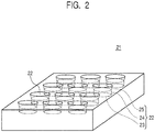
- FIG. 2 is an enlarged view of the toric surface 2 having the fine uneven structure of FIG. 1 .
- the toric surface 2 is simplified and illustrated as a flat surface though the toric surface 2 is a curved surface.
- the fine uneven structure is formed in an optically effective region of the toric surface 2 of the toric lens 21.
- the fine uneven structure is a fine uneven structure including a plurality of holes 22.
- each of the holes 22 has a bottom surface 23 and a side surface extending between the bottom surface 23 and the surface 2 of the toric surface 21.
- a hole structure 24 proximal to the bottom surface 23 of each of the holes 22 has a cylindrical shape and a hole structure 25 distal to the bottom surface 23, that is, between the hole structure 24 and the toric surface 21 has a circular truncated cone shape with a gradually increasing diameter toward the surface 2.
- FIG. 3 is a sectional view of the holes 22. It is preferred that a hole depth H of the hole 22 be 80 nm or more and 185 nm or less, more preferably 100 nm or more and 165 nm or less. In addition, it is preferred that a height "nb" of the hole structure 24 having a cylindrical shape on the bottom surface 23 side be 30 nm or more and 90 nm or less, more preferably 40 nm or more and 79 nm or less. It is preferred that a height "ht" of the hole structure 25 having a circular truncated cone shape on the surface side of the hole 22 be 25 nm or more and 105 nm or less, more preferably 34 nm or more and 95 nm or less.
- an opening diameter " ⁇ t" of the hole 22 be 150 nm or more and 450 nm or less, more preferably 198 nm or more and 407 nm or less. It is preferred that a diameter " ⁇ b" of the bottom surface 23 be 30 nm or more and 90 nm or less, more preferably 40 nm or more and 79 nm or less.
- the hole depth H and the surface opening diameter " ⁇ t" satisfy an expression of 0.3 ⁇ H/ ⁇ t ⁇ 0.6.
- H/ ⁇ t an aspect ratio
- antireflection performance is decreased.
- H/ ⁇ t > 0.6 a high pressure is required in injection molding, with the result that the shape accuracy of a lens surface is deteriorated.
- an angle ⁇ formed between an opening portion and the surface of the hole 22 satisfy an expression of 78° ⁇ ⁇ ⁇ 85°.
- 85° ⁇ ⁇ is satisfied, the reproducibility of a fine uneven structure dimension in injection molding is decreased.
- 78° > ⁇ is satisfied, the antireflection effect is decreased.
- the hole 22 satisfy an expression of 0.109 ⁇ ( ⁇ t- ⁇ b)/H ⁇ 0.163.
- 0.109 > ( ⁇ t- ⁇ b)/H is satisfied, the surface accuracy of the optical element is decreased.
- ( ⁇ t- ⁇ b)/H > 0.163 is satisfied, the antireflection performance is decreased.
- an average pitch interval P of the holes 22 be 100 nm or more and 1 ⁇ m or less, more preferably 250 nm or more and 500 nm or less.
- the average pitch interval P is less than 100 nm, the strength is decreased.
- the average pitch interval P is more than 1 ⁇ m, the antireflection performance is decreased.
- the average pitch interval of the holes 22 refers to a distance between a hole and a hole located at a closest distance from the hole on the surface of the optical element.
- the average pitch interval P is determined by averaging pitch distances of 100 holes in a SEM image.
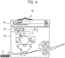
- FIG. 4 is a view for illustrating a copying machine serving as the image forming apparatus.
- a copying machine 41 includes an image reading unit 42 and an image forming unit 43.
- the image forming unit 43 includes an image bearing member, a charging unit, an exposing unit, and a developing unit.
- the charging unit is configured to charge a surface of the image bearing member.
- the exposing unit is configured to expose the image bearing member to light through use of a laser optical system 44.
- the developing unit is configured to develop an electrostatic latent image formed on the surface of the image bearing member with a developer.
- the image forming unit 43 further includes a transfer unit and a fixing unit.
- the transfer unit is configured to transfer a developed image of the developer to a sheet.
- the fixing unit is configured to fix the developer transferred onto the sheet.
- the above-mentioned toric lens can be used in an f- ⁇ lens of the laser optical system 44.
- the optical element according to at least one embodiment has the fine uneven structure on an optical surface, and can be manufactured by injection molding.
- An injection molding piece having an uneven structure on at least one surface is prepared.
- the injection molding piece can be manufactured by the following method. First, a fine uneven structure is formed on a surface of a mirror surface piece for injection molding.
- a plating film 52 made of NiP is grown on a base material 51 made of STAVAX, and after that, the surface of the plating film 52 is smoothened.
- a SiO 2 film 53 is formed on the surface of the plating film 52 to a uniform thickness of 100 nm or more and 300 nm or less by sputtering.
- the SiO 2 film 53 is formed by finely adjusting a ratio of an Ar gas and an O 2 gas through use of a Si target.
- a film rich in Si is formed in the SiO 2 film 53 on a side close to the plating film 52.
- the SiO 2 film having a thickness equal to or more than the depth of the hole 22 of the fine uneven structure is formed on a side away from the plating film 52.
- a photoresist 54 is applied to the surface of the SiO 2 film 53 to a uniform film thickness by spin coating.
- the resultant is subjected to drying treatment such as prebaking. Then, as illustrated in FIG. 5D , patterns each having a substantially cylindrical shape are drawn in a direction perpendicular to a curved surface of the mirror surface piece by electron beam drawing.
- Fine uneven structure patterns each having, in the substantially cylindrical shape, a cylindrical shape in a lower stage and a circular truncated cone shape having a hole diameter decreasing toward the surface in an upper stage, are formed at an average pitch interval of 100 nm or more and 1 ⁇ m or less, preferably 250 nm or more and 500 nm or less.
- a molten resin is filled between the fine uneven structure patterns at a high pressure of 40 MPa or more, and hence the resin is swollen through stress relaxation after molding release. It is required that the size of each of the fine uneven structure patterns be corrected for shape in consideration of stress relaxation as compared to a hole diameter in size to be finally obtained in a molded product.
- the cylindrical shape in the lower stage of each of the fine uneven structure patterns formed on the piece surface is drawn so that the diameter thereof becomes thicker by a little more than 20 nm because gaps between the respective adjacent patterns become narrower and swelling is strengthened in molding release
- the circular truncated cone shape in the upper stage of each of the fine uneven structure patterns is drawn so that the diameter thereof becomes thicker by a little less than 10 nm because gaps between the respective adjacent patterns are enlarged and the swelling is weakened in molding release.
- the thickness of the photoresist 54 used in a drawing step is related to the fine uneven structure formed on the surface of the mirror surface piece. Specifically, when the height of the fine uneven structure is set to 120 nm, the thickness of the photoresist 54 of 90 nm or more is required based on the selection ratio in dry etching.
- interface reflection is appropriately reduced by treatment of bark and talc in accordance with the specifications of a drawing device or the like.
- Drawing patterns are formed by immersing the mirror surface piece after drawing in a developing solution. After that, the resultant is subjected to postbaking treatment. With this, similar patterns in which the fine uneven structure to be formed by dry etching is reduced in a height direction are formed on the SiO 2 film.
- the SiO 2 film is etched by a thickness of 120 nm by dry etching using a CHF3 gas with the photoresist 54 being a mask, to thereby uniformly form the fine uneven structure with a period equal to or less than a wavelength of preventing reflection on the surface of the mirror surface piece.
- Ashing treatment is performed with an oxygen gas after dry etching to remove a residue of the photoresist 54, and thus a mirror surface piece for injection molding including a SiO 2 film 53a having a fine uneven structure formed thereon is manufactured.
- a fine uneven structure is uniformly formed also on the surface of the injection molding piece on an opposite side in a similar manner.
- a method of forming a fine uneven structure with a period equal to or less than a wavelength of preventing reflection on the surface of the mirror surface piece for injection molding is not limited to the method described above.
- pieces 61a and 61b each having fine uneven structure patterns formed on the surface of the mirror surface piece are incorporated into a fixed-side mold 62a and a movable-side mold 62b of an injection molding device, respectively, and an optical element having a fine uneven structure configured to exhibit an antireflection function is formed by injection molding.
- an uncured resin 63 is molded through a resin injection step of injecting the uncured resin 63 into between a set of pieces.
- a thermoplastic resin such as a cycloolefin polymer resin having less water-absorbing property, a polycarbonate resin, or a polymethyl methacrylate resin can be used. Of those, it is preferred that the cycloolefin polymer resin having less water-absorbing property be used.
- the molten resin temperature be 250°C or more and 290°C or less
- the mold temperature be 125°C or more and 140°C or less
- the holding pressure be 20 MPa or more and 90 MPa or less.
- the fine uneven structure on the piece surface has a two-stage structure in which the circular truncated cone shape having an upper hole diameter decreasing is laminated on the cylindrical shape.
- such fine shape is not directly transferred onto the molded optical element obtained by injection molding.
- a hole structure having a cylindrical shape is formed on a substrate side, and a hole structure having a circular truncated cone shape with an opening diameter increasing toward a surface side is formed.
- the molten resin is filled into between the set of pieces, followed by transfer at a high pressure. Therefore, stress relaxation occurs after molding, and a cylindrical hole having a substantially perpendicular shape is formed in a part having the circular truncated cone shape of the piece.
- a circular truncated cone shape having an opening diameter increasing toward the surface is formed in a part having the cylindrical shape of the piece due to stress relaxation.
- the cylindrical hole diameter is narrowed by about a little less than 10 nm on the substrate side of the molded product, and the opening diameter of the circular truncated cone hole on the surface side is narrowed by about a little less than 20 nm.
- an antireflection optical member in which a shape correction amount of the fine uneven structure formed on the piece is reflected, is obtained.
- a two-stage structure is formed in the molded optical member obtained by injection molding under a condition of a piece structure having a stress relaxation amount controlled.
- a hole structure having a cylindrical shape configured to decrease reflectance is formed on the substrate side, and a side wall inclined portion contributing to reflection is decreased accordingly.
- the optical element having the fine uneven structure on the surface of the present invention is excellent in antireflection performance, and a manufacturing cost can be reduced.
- Reflectance was measured through use of a microscopic spectroscopic device (USPM-RUII manufactured by Olympus Corporation).
- the measurement conditions were an objective lens magnification of 10 times, and a measurement wavelength of from 380 nm to 780 nm.
- a local minimum value of reflectance was represented by Rmin.
- an injection molding piece was manufactured by the following method.
- a set of mirror surface pieces, on each of which a fine uneven structure was to be formed, were manufactured.
- the set of mirror surface pieces had a concave shape and a convex shape, respectively, and each had a dimension of 20 nm in a longitudinal direction and a dimension of 5 nm in a short direction.
- the plating film 52 made of NiP was grown on the base material 51 made of STAVAX, and after that, the surface of the plating film 52 was subjected to mirror finishing so that the thickness of the plating film 52 of about 30 ⁇ m was left in accordance with a lens surface.
- the SiO 2 film 53 was formed on the NiP surface to a uniform thickness of 200 nm by sputtering.
- the SiO 2 film 53 first, a film rich in Si was formed on the NiP surface, and then the SiO 2 film was formed in the thickness corresponding to the depth of the fine uneven structure.
- the photoresist 54 was applied to the surface of the SiO 2 film 53 to a uniform film thickness by spin coating.
- patterns each having a substantially cylindrical shape were drawn in a direction perpendicular to a curved surface of the mirror surface piece by electron beam drawing.
- Fine uneven structure patterns each having, in the substantially cylindrical shape, a cylindrical shape in a lower stage and a circular truncated cone shape having a hole diameter decreasing toward a surface in an upper stage, were formed at an average pitch interval of 250 nm.
- the lower stage was formed into a cylindrical shape having a diameter of about 228 nm and a height of about 54 nm.
- the upper stage was formed into a circular truncated cone shape having a height of about 56 nm with a taper angle of about 79 degrees.
- an uncured cycloolefin resin was injected into between the set of molding pieces and molded. It is preferred that the cycloolefin resin be molded at a molten resin temperature of 270°C, a mold temperature of 140°C or less, and a holding pressure of from 20 MPa or more and 90 MPa or less. In addition, the molding was performed at an injection molding speed of 30 mm/sec.
- the resultant was cooled and released from the molds to obtain an optical element.
- the fine uneven structure on the surface of the optical element had a shape as shown in Table 1.
- the depth of the hole structure having a substantially circular truncated cone shape with an inclined side surface can be set to be as small as 54 nm though the aspect ratio is as low as 0.53. Therefore, there is an effect of suppressing an increase in reflectance with respect to a set wavelength in ordinary injection molding.
- Comparative Example 1 an optical element, in which a side wall of a fine hole structure was formed substantially perpendicularly, was manufactured in the same manner as in Example 1 except that the cylindrical shape formed on the molding piece was changed, and that the injection molding speed was set to be extremely low to about 2 mm/sec to perform molding.
- the molded resin did not sufficiently reach a side opposite to an injection gate due to the low injection molding speed, and the fine uneven structure on the side opposite to the injection gate was formed to be smaller than a desired height, with the result that reflectance was significantly increased.
- the height of the fine uneven structure on the side opposite to the injection gate was about 40 nm, and reflectance was about 1%.
- Example 2 an optical element, in which a side wall of a fine hole structure was formed substantially perpendicularly, was manufactured in the same manner as in Example 1 except that the cylindrical shape formed on the molding piece was changed.
- the cylindrical shape was formed in portions on the molding piece at pitch intervals of 250 nm.
- the substantially cylindrical shape the lower stage was formed into a cylindrical shape having a diameter of about 218 nm and a height of about 41 nm.
- the upper stage was formed into a circular truncated cone shape having a height of about 79 nm with a taper angle of about 81 degrees.
- Example 3 an optical element, in which a side wall of a fine hole structure was formed substantially perpendicularly, was manufactured in the same manner as in Example 1 except that the cylindrical shape formed on the molding piece was changed.
- the cylindrical shape was formed in portions on the molding piece at pitch intervals of about 250 nm.
- the substantially cylindrical shape the lower stage was formed into a cylindrical shape having a diameter of about 218 nm and a height of about 34 nm.
- the upper stage was formed into a circular truncated cone shape having a height of about 66 nm with a taper angle of about 79 degrees.
- Example 4 an optical element, in which a side wall of a fine hole structure was formed substantially perpendicularly, was manufactured in the same manner as in Example 1 except that the cylindrical shape formed on the molding piece was changed.
- the cylindrical shape was formed in portions on the molding piece at pitch intervals of about 250 nm.
- the lower stage was formed into a cylindrical shape having a diameter of about 228 nm and a height of about 70 nm.
- the upper stage was formed into a circular truncated cone shape having a height of about 40 nm with a taper angle of about 75 degrees.
- Example 5 an optical element, in which a side wall of a fine hole structure was formed substantially perpendicularly, was manufactured in the same manner as in Example 1 except that the cylindrical shape formed on the molding piece was changed.
- the cylindrical shape was formed in portions on the molding piece at pitch intervals of about 500 nm.
- the lower stage was formed into a cylindrical shape having a diameter of about 427 nm and a height of about 95 nm.
- the upper stage was formed into a circular truncated cone shape having a height of about 70 nm with a taper angle of about 75 degrees.
- Comparative Example 2 an optical element, in which a side wall of a fine hole structure was formed substantially perpendicularly, was manufactured in the same manner as in Example 1 except that the cylindrical shape formed on the molding piece was changed, and that the injection molding speed was set to 30 mm/sec to perform molding.
- the molded resin was not sufficiently filled into the fine uneven structure of the piece. Therefore, the reflection characteristics of molded products were varied due to slight variation in injection molding conditions, and reproducibility was decreased. Specifically, the value of 3 ⁇ was about 0.05, and molded products having a reflectance of about 0.1% were also included.
- the depth of the hole structure having a substantially circular truncated cone shape with an inclined side surface can be set to be as small as 54 nm although the aspect ratio is as low as 0.53. Therefore, there is an effect of suppressing an increase in reflectance with respect to a set wavelength in ordinary injection molding.
- Embodiment(s) of the present invention can also be realized by a computer of a system or apparatus that reads out and executes computer executable instructions (e.g., one or more programs) recorded on a storage medium (which may also be referred to more fully as a 'non-transitory computer-readable storage medium') to perform the functions of one or more of the above-described embodiment(s) and/or that includes one or more circuits (e.g., application specific integrated circuit (ASIC)) for performing the functions of one or more of the above-described embodiment(s), and by a method performed by the computer of the system or apparatus by, for example, reading out and executing the computer executable instructions from the storage medium to perform the functions of one or more of the above-described embodiment(s) and/or controlling the one or more circuits to perform the functions of one or more of the above-described embodiment(s).
- computer executable instructions e.g., one or more programs
- a storage medium which may also be referred to more fully as
- the computer may comprise one or more processors (e.g., central processing unit (CPU), micro processing unit (MPU)) and may include a network of separate computers or separate processors to read out and execute the computer executable instructions.
- the computer executable instructions may be provided to the computer, for example, from a network or the storage medium.
- the storage medium may include, for example, one or more of a hard disk, a random-access memory (RAM), a read only memory (ROM), a storage of distributed computing systems, an optical disk (such as a compact disc (CD), digital versatile disc (DVD), or Blu-ray Disc (BD)TM), a flash memory device, a memory card, and the like.
Landscapes
- Physics & Mathematics (AREA)
- Engineering & Computer Science (AREA)
- General Physics & Mathematics (AREA)
- Optics & Photonics (AREA)
- Health & Medical Sciences (AREA)
- Manufacturing & Machinery (AREA)
- Ophthalmology & Optometry (AREA)
- Mechanical Engineering (AREA)
- Multimedia (AREA)
- Signal Processing (AREA)
- Moulds For Moulding Plastics Or The Like (AREA)
- Surface Treatment Of Optical Elements (AREA)
Abstract
Description
- The present disclosure relates to an optical element such as a toric lens having a fine uneven structure (microstructure) on a surface thereof, and an image forming apparatus including a laser scanning optical system using the optical element.
- An optical component having a fine uneven structure with a period smaller than a wavelength of light expresses an antireflection structure, and hence there has hitherto been proposed such optical component having a fine uneven structure.
- In Japanese Patent Application Laid-Open No.
2007-171857 2007-171857 - However, in the optical component disclosed in Japanese Patent Application Laid-Open No.
2007-171857 - According to one aspect of the present invention, there is provided a toric lens comprising a toric surface having a fine uneven structure, wherein: the fine uneven structure includes a plurality of holes; the plurality of holes has a hole depth H and a surface opening diameter ϕt which satisfy an expression of 0.3 ≤ H/ϕt ≤ 0.6; and (a) the plurality of holes has a cylindrical shape proximal to a bottom surface and a circular truncated cone shape distal to the bottom surface, the circularly truncated cone shape having a diameter gradually increasing toward a top surface of the toric surface, or (b) an angle θ formed between the top surface of the toric surface and a side surface of the plurality of holes satisfies 78° ≤ θ ≤ 85°.
- According to another aspect of the present invention, there is provided an optical element comprising an optical surface having a fine uneven structure, wherein: the fine uneven structure includes a plurality of holes; the plurality of holes has a hole depth H and a surface opening diameter ϕt which satisfy an expression of 0.3 ≤ H/ϕt ≤ 0.6; and (a) the plurality of holes has a cylindrical shape proximal to a bottom surface thereof and a circular truncated cone shape distal to the bottom surface, the circulated truncated cone shape having a diameter gradually increasing toward a surface of the toric surface, or (b) an angle θ between the top surface of the toric surface and a side surface of the plurality of holes satisfies 78° ≤ θ ≤ 85°.
- According to still another aspect of the present invention, there is provided an image forming apparatus comprising: an image bearing member; a charging unit configured to charge a surface of the image bearing member; an exposing unit configured to expose the image bearing member to light using a laser optical system; and a developing unit configured to, using a developer, develop an electrostatic latent image formed on the surface of the image bearing member, wherein the laser optical system including a toric lens comprising a toric surface having a fine uneven structure, wherein: the fine uneven structure includes a plurality of holes; the plurality of holes has a hole depth H and a surface opening diameter ϕt which satisfy an expression of 0.3 ≤ H/ϕt ≤ 0.6; and (a) the plurality of holes has a cylindrical shape proximal to a bottom surface and a circular truncated cone shape distal to the bottom surface, the circularly truncated cone shape having a diameter gradually increasing toward a top surface of the toric surface, or (b) an angle θ formed between the top surface of the toric surface and a side surface of the plurality of holes satisfies 78° ≤ θ ≤ 85°.
- Further features of the present invention will become apparent from the following description of exemplary embodiments with reference to the attached drawings.
-
-
FIG. 1 is a schematic view of a toric lens according to at least one embodiment of the present invention. -
FIG. 2 is a schematic view for illustrating a fine uneven structure of an optical element according to at least one embodiment of the present invention. -
FIG. 3 is a schematic view for illustrating holes of the fine uneven structure of the optical element according to at least one embodiment of the present invention. -
FIG. 4 is a schematic view for illustrating an image forming apparatus according to at least one embodiment of the present invention. -
FIG. 5A, FIG. 5B, FIG. 5C, and FIG. 5D are each a view for illustrating a method of manufacturing an injection molding piece in at least one embodiment of the present invention. -
FIG. 6A, FIG. 6B, and FIG. 6C are each a view for illustrating a method of manufacturing an optical element according to at least one embodiment of the present invention. - A detailed description is now given of at least one embodiment of the present invention referring to drawings.
- An optical element according to at least one embodiment of the present invention has a feature in that the optical element has antireflection performance due to a fine uneven structure formed on a curved surface.
- As the optical element according to at least one embodiment, a mirror, a lens, a prism, or the like can be used. As the lens, a toric lens as illustrated in
FIG. 1 can be used. At least one embodiment is described below through use of the toric lens. - As illustrated in
FIG. 1 , atoric lens 1 refers to a lens in which one surface of the lens is formed of atoric surface 2. Such toric lens is used as a component of an f-θ lens in order to correct an optical face tangle error in a laser scanning optical system. A fine uneven structure (not shown) for antireflection is formed in an effective region of thetoric surface 2. It is preferred that the fine uneven structure be an injection molding formed by injection molding. - The
toric lens 1 according to at least one embodiment may be formed of a single member or a plurality of members including a member having a fine uneven structure on a curved surface and another member. - As the member having a fine uneven structure and the member other than the member having a fine uneven structure, a polycarbonate resin, a polymethyl methacrylate resin, or a cycloolefin polymer resin can be used. Of those, it is preferred that the cycloolefin polymer resin having less water-absorbing property be used.
-
FIG. 2 is an enlarged view of thetoric surface 2 having the fine uneven structure ofFIG. 1 . InFIG. 2 , thetoric surface 2 is simplified and illustrated as a flat surface though thetoric surface 2 is a curved surface. As illustrated inFIG. 2 , the fine uneven structure is formed in an optically effective region of thetoric surface 2 of thetoric lens 21. The fine uneven structure is a fine uneven structure including a plurality ofholes 22. Preferably but optionally, each of theholes 22 has abottom surface 23 and a side surface extending between thebottom surface 23 and thesurface 2 of thetoric surface 21. Ahole structure 24 proximal to thebottom surface 23 of each of theholes 22 has a cylindrical shape and ahole structure 25 distal to thebottom surface 23, that is, between thehole structure 24 and thetoric surface 21 has a circular truncated cone shape with a gradually increasing diameter toward thesurface 2. -
FIG. 3 is a sectional view of theholes 22. It is preferred that a hole depth H of thehole 22 be 80 nm or more and 185 nm or less, more preferably 100 nm or more and 165 nm or less. In addition, it is preferred that a height "nb" of thehole structure 24 having a cylindrical shape on thebottom surface 23 side be 30 nm or more and 90 nm or less, more preferably 40 nm or more and 79 nm or less. It is preferred that a height "ht" of thehole structure 25 having a circular truncated cone shape on the surface side of thehole 22 be 25 nm or more and 105 nm or less, more preferably 34 nm or more and 95 nm or less. - It is preferred that an opening diameter "φt" of the
hole 22 be 150 nm or more and 450 nm or less, more preferably 198 nm or more and 407 nm or less. It is preferred that a diameter "φb" of thebottom surface 23 be 30 nm or more and 90 nm or less, more preferably 40 nm or more and 79 nm or less. - It is preferred that, in an aspect ratio (H/φt) of the
hole 22, the hole depth H and the surface opening diameter "φt" satisfy an expression of 0.3 ≤ H/φt ≤ 0.6. When 0.3 > H/φt is satisfied, antireflection performance is decreased. When H/φt > 0.6 is satisfied, a high pressure is required in injection molding, with the result that the shape accuracy of a lens surface is deteriorated. - It is preferred that an angle θ formed between an opening portion and the surface of the
hole 22 satisfy an expression of 78° ≤ θ ≤ 85°. When 85° < θ is satisfied, the reproducibility of a fine uneven structure dimension in injection molding is decreased. When 78° > θ is satisfied, the antireflection effect is decreased. - It is preferred that the
hole 22 satisfy an expression of 0.109 ≤ (φt-φb)/H ≤ 0.163. When 0.109 > (φt-φb)/H is satisfied, the surface accuracy of the optical element is decreased. When (φt-φb)/H > 0.163 is satisfied, the antireflection performance is decreased. - It is preferred that an average pitch interval P of the
holes 22 be 100 nm or more and 1 µm or less, more preferably 250 nm or more and 500 nm or less. When the average pitch interval P is less than 100 nm, the strength is decreased. When the average pitch interval P is more than 1 µm, the antireflection performance is decreased. In this case, the average pitch interval of theholes 22 refers to a distance between a hole and a hole located at a closest distance from the hole on the surface of the optical element. The average pitch interval P is determined by averaging pitch distances of 100 holes in a SEM image. - An image forming apparatus (electrophotographic apparatus) according to at least one embodiment of the present invention can be used in a copying machine and a multifunctional peripheral, which have a laser optical system using an optical element such as the above-mentioned toric lens.
FIG. 4 is a view for illustrating a copying machine serving as the image forming apparatus. A copyingmachine 41 includes animage reading unit 42 and animage forming unit 43. Theimage forming unit 43 includes an image bearing member, a charging unit, an exposing unit, and a developing unit. The charging unit is configured to charge a surface of the image bearing member. The exposing unit is configured to expose the image bearing member to light through use of a laseroptical system 44. The developing unit is configured to develop an electrostatic latent image formed on the surface of the image bearing member with a developer. Theimage forming unit 43 further includes a transfer unit and a fixing unit. The transfer unit is configured to transfer a developed image of the developer to a sheet. The fixing unit is configured to fix the developer transferred onto the sheet. The above-mentioned toric lens can be used in an f-θ lens of the laseroptical system 44. - Next, a method of manufacturing an optical element according to at least one embodiment of the present invention is described.
- The optical element according to at least one embodiment has the fine uneven structure on an optical surface, and can be manufactured by injection molding. An injection molding piece having an uneven structure on at least one surface is prepared.
- The injection molding piece can be manufactured by the following method. First, a fine uneven structure is formed on a surface of a mirror surface piece for injection molding.
- As illustrated in
FIG. 5A , as a mirror surface piece on which a fine uneven structure is to be formed, aplating film 52 made of NiP is grown on abase material 51 made of STAVAX, and after that, the surface of theplating film 52 is smoothened. - After the surface of the
plating film 52 is washed, as illustrated inFIG. 5B , a SiO2 film 53 is formed on the surface of theplating film 52 to a uniform thickness of 100 nm or more and 300 nm or less by sputtering. In the sputtering, the SiO2 film 53 is formed by finely adjusting a ratio of an Ar gas and an O2 gas through use of a Si target. - In order to control the etching depth of the SiO2 film 53 with an etching selection ratio of a film composition by dry etching in a back-end process, a film rich in Si is formed in the SiO2 film 53 on a side close to the
plating film 52. In addition, the SiO2 film having a thickness equal to or more than the depth of thehole 22 of the fine uneven structure is formed on a side away from theplating film 52. - As illustrated in
FIG. 5C , aphotoresist 54 is applied to the surface of the SiO2 film 53 to a uniform film thickness by spin coating. - The resultant is subjected to drying treatment such as prebaking. Then, as illustrated in
FIG. 5D , patterns each having a substantially cylindrical shape are drawn in a direction perpendicular to a curved surface of the mirror surface piece by electron beam drawing. - Fine uneven structure patterns, each having, in the substantially cylindrical shape, a cylindrical shape in a lower stage and a circular truncated cone shape having a hole diameter decreasing toward the surface in an upper stage, are formed at an average pitch interval of 100 nm or more and 1 µm or less, preferably 250 nm or more and 500 nm or less.
- In injection molding, a molten resin is filled between the fine uneven structure patterns at a high pressure of 40 MPa or more, and hence the resin is swollen through stress relaxation after molding release. It is required that the size of each of the fine uneven structure patterns be corrected for shape in consideration of stress relaxation as compared to a hole diameter in size to be finally obtained in a molded product.
- Although it also relates to injection molding conditions and the like, the cylindrical shape in the lower stage of each of the fine uneven structure patterns formed on the piece surface is drawn so that the diameter thereof becomes thicker by a little more than 20 nm because gaps between the respective adjacent patterns become narrower and swelling is strengthened in molding release, and the circular truncated cone shape in the upper stage of each of the fine uneven structure patterns is drawn so that the diameter thereof becomes thicker by a little less than 10 nm because gaps between the respective adjacent patterns are enlarged and the swelling is weakened in molding release.
- The thickness of the
photoresist 54 used in a drawing step is related to the fine uneven structure formed on the surface of the mirror surface piece. Specifically, when the height of the fine uneven structure is set to 120 nm, the thickness of thephotoresist 54 of 90 nm or more is required based on the selection ratio in dry etching. - Regarding the
photoresist 54, interface reflection is appropriately reduced by treatment of bark and talc in accordance with the specifications of a drawing device or the like. - Drawing patterns are formed by immersing the mirror surface piece after drawing in a developing solution. After that, the resultant is subjected to postbaking treatment. With this, similar patterns in which the fine uneven structure to be formed by dry etching is reduced in a height direction are formed on the SiO2 film. The SiO2 film is etched by a thickness of 120 nm by dry etching using a CHF3 gas with the
photoresist 54 being a mask, to thereby uniformly form the fine uneven structure with a period equal to or less than a wavelength of preventing reflection on the surface of the mirror surface piece. Ashing treatment is performed with an oxygen gas after dry etching to remove a residue of thephotoresist 54, and thus a mirror surface piece for injection molding including a SiO2 film 53a having a fine uneven structure formed thereon is manufactured. - A fine uneven structure is uniformly formed also on the surface of the injection molding piece on an opposite side in a similar manner.
- A method of forming a fine uneven structure with a period equal to or less than a wavelength of preventing reflection on the surface of the mirror surface piece for injection molding is not limited to the method described above.
- Next, as illustrated in
FIG. 6A ,pieces side mold 62a and a movable-side mold 62b of an injection molding device, respectively, and an optical element having a fine uneven structure configured to exhibit an antireflection function is formed by injection molding. - As illustrated in
FIG. 6B , anuncured resin 63 is molded through a resin injection step of injecting theuncured resin 63 into between a set of pieces. As the resin for injection molding, a thermoplastic resin such as a cycloolefin polymer resin having less water-absorbing property, a polycarbonate resin, or a polymethyl methacrylate resin can be used. Of those, it is preferred that the cycloolefin polymer resin having less water-absorbing property be used. When the cycloolefin polymer resin is used, it is preferred that the molten resin temperature be 250°C or more and 290°C or less, the mold temperature be 125°C or more and 140°C or less, and the holding pressure be 20 MPa or more and 90 MPa or less. - As illustrated in
FIG. 6C , after the molded resin temperature is cooled to a temperature equal to or less than a glass transition temperature, a molded product is released so as not to be inclined through use of an ejector pin, to thereby obtain anoptical element 63a. - The fine uneven structure on the piece surface has a two-stage structure in which the circular truncated cone shape having an upper hole diameter decreasing is laminated on the cylindrical shape. However, such fine shape is not directly transferred onto the molded optical element obtained by injection molding. A hole structure having a cylindrical shape is formed on a substrate side, and a hole structure having a circular truncated cone shape with an opening diameter increasing toward a surface side is formed.
- The molten resin is filled into between the set of pieces, followed by transfer at a high pressure. Therefore, stress relaxation occurs after molding, and a cylindrical hole having a substantially perpendicular shape is formed in a part having the circular truncated cone shape of the piece. In addition, a circular truncated cone shape having an opening diameter increasing toward the surface is formed in a part having the cylindrical shape of the piece due to stress relaxation. In stress relaxation, the cylindrical hole diameter is narrowed by about a little less than 10 nm on the substrate side of the molded product, and the opening diameter of the circular truncated cone hole on the surface side is narrowed by about a little less than 20 nm. Therefore, an antireflection optical member, in which a shape correction amount of the fine uneven structure formed on the piece is reflected, is obtained. In the molded optical member obtained by injection molding under a condition of a piece structure having a stress relaxation amount controlled, a two-stage structure is formed. In the two-stage structure, a hole structure having a cylindrical shape configured to decrease reflectance is formed on the substrate side, and a side wall inclined portion contributing to reflection is decreased accordingly.
- The optical element having the fine uneven structure on the surface of the present invention is excellent in antireflection performance, and a manufacturing cost can be reduced.
- In the method of manufacturing an optical element such as the toric lens of the present invention, a fine uneven structure is formed by injection molding. Therefore, the manufacturing time can be shortened, and the manufacturing cost can be reduced.
- In the following Examples and Comparative Examples, manufactured optical elements were evaluated by the following methods.
- Reflectance was measured through use of a microscopic spectroscopic device (USPM-RUII manufactured by Olympus Corporation). The measurement conditions were an objective lens magnification of 10 times, and a measurement wavelength of from 380 nm to 780 nm. In addition, in the obtained reflection spectral characteristics, a local minimum value of reflectance was represented by Rmin.
- First, an injection molding piece was manufactured by the following method.
- As illustrated in
FIG. 5A , a set of mirror surface pieces, on each of which a fine uneven structure was to be formed, were manufactured. The set of mirror surface pieces had a concave shape and a convex shape, respectively, and each had a dimension of 20 nm in a longitudinal direction and a dimension of 5 nm in a short direction. Theplating film 52 made of NiP was grown on thebase material 51 made of STAVAX, and after that, the surface of theplating film 52 was subjected to mirror finishing so that the thickness of theplating film 52 of about 30 µm was left in accordance with a lens surface. - Next, as illustrated in
FIG. 5B , after the mirror surface of NiP was washed, the SiO2 film 53 was formed on the NiP surface to a uniform thickness of 200 nm by sputtering. In the SiO2 film 53, first, a film rich in Si was formed on the NiP surface, and then the SiO2 film was formed in the thickness corresponding to the depth of the fine uneven structure. - As illustrated in
FIG. 5C , thephotoresist 54 was applied to the surface of the SiO2 film 53 to a uniform film thickness by spin coating. - After drying treatment, as illustrated in
FIG. 5D , patterns each having a substantially cylindrical shape were drawn in a direction perpendicular to a curved surface of the mirror surface piece by electron beam drawing. Fine uneven structure patterns, each having, in the substantially cylindrical shape, a cylindrical shape in a lower stage and a circular truncated cone shape having a hole diameter decreasing toward a surface in an upper stage, were formed at an average pitch interval of 250 nm. In Example 1, in the substantially cylindrical shape, the lower stage was formed into a cylindrical shape having a diameter of about 228 nm and a height of about 54 nm. In addition, the upper stage was formed into a circular truncated cone shape having a height of about 56 nm with a taper angle of about 79 degrees. - As illustrated in
FIG. 6A , a set of molding pieces thus manufactured, each having the fine uneven structure patterns formed on the surface of the mirror surface piece, were incorporated into a fixed side and a movable side of the injection molding device, respectively, and an optical element having a fine uneven structure with a period equal to or less than a wavelength of exhibiting an antireflection function was formed by injection molding. - As illustrated in
FIG. 6B , an uncured cycloolefin resin was injected into between the set of molding pieces and molded. It is preferred that the cycloolefin resin be molded at a molten resin temperature of 270°C, a mold temperature of 140°C or less, and a holding pressure of from 20 MPa or more and 90 MPa or less. In addition, the molding was performed at an injection molding speed of 30 mm/sec. - As illustrated in
FIG. 6C , the resultant was cooled and released from the molds to obtain an optical element. The fine uneven structure on the surface of the optical element had a shape as shown in Table 1. - In the hole structure having a two-stage structure in Example 1, the depth of the hole structure having a substantially circular truncated cone shape with an inclined side surface can be set to be as small as 54 nm though the aspect ratio is as low as 0.53. Therefore, there is an effect of suppressing an increase in reflectance with respect to a set wavelength in ordinary injection molding.
- In Comparative Example 1, an optical element, in which a side wall of a fine hole structure was formed substantially perpendicularly, was manufactured in the same manner as in Example 1 except that the cylindrical shape formed on the molding piece was changed, and that the injection molding speed was set to be extremely low to about 2 mm/sec to perform molding.
- Each dimension and characteristics of the fine uneven structure of the optical element are shown in Table 1.
- In the optical element of Comparative Example 1, the molded resin did not sufficiently reach a side opposite to an injection gate due to the low injection molding speed, and the fine uneven structure on the side opposite to the injection gate was formed to be smaller than a desired height, with the result that reflectance was significantly increased. Specifically, the height of the fine uneven structure on the side opposite to the injection gate was about 40 nm, and reflectance was about 1%.
- In Example 2, an optical element, in which a side wall of a fine hole structure was formed substantially perpendicularly, was manufactured in the same manner as in Example 1 except that the cylindrical shape formed on the molding piece was changed. In Example 2, the cylindrical shape was formed in portions on the molding piece at pitch intervals of 250 nm. In the substantially cylindrical shape, the lower stage was formed into a cylindrical shape having a diameter of about 218 nm and a height of about 41 nm. In addition, the upper stage was formed into a circular truncated cone shape having a height of about 79 nm with a taper angle of about 81 degrees.
- Each dimension and characteristics of the fine uneven structure of the optical element are shown in Table 1.
- In Example 3, an optical element, in which a side wall of a fine hole structure was formed substantially perpendicularly, was manufactured in the same manner as in Example 1 except that the cylindrical shape formed on the molding piece was changed. In Example 3, the cylindrical shape was formed in portions on the molding piece at pitch intervals of about 250 nm. In the substantially cylindrical shape, the lower stage was formed into a cylindrical shape having a diameter of about 218 nm and a height of about 34 nm. In addition, the upper stage was formed into a circular truncated cone shape having a height of about 66 nm with a taper angle of about 79 degrees.
- Each dimension and characteristics of the fine uneven structure of the optical element are shown in Table 1.
- In Example 4, an optical element, in which a side wall of a fine hole structure was formed substantially perpendicularly, was manufactured in the same manner as in Example 1 except that the cylindrical shape formed on the molding piece was changed. In Example 4, the cylindrical shape was formed in portions on the molding piece at pitch intervals of about 250 nm. In the cylindrical shape, the lower stage was formed into a cylindrical shape having a diameter of about 228 nm and a height of about 70 nm. In addition, the upper stage was formed into a circular truncated cone shape having a height of about 40 nm with a taper angle of about 75 degrees.
- Each dimension and characteristics of the fine uneven structure of the optical element are shown in Table 1.
- In Example 5, an optical element, in which a side wall of a fine hole structure was formed substantially perpendicularly, was manufactured in the same manner as in Example 1 except that the cylindrical shape formed on the molding piece was changed. In Example 5, the cylindrical shape was formed in portions on the molding piece at pitch intervals of about 500 nm. In the cylindrical shape, the lower stage was formed into a cylindrical shape having a diameter of about 427 nm and a height of about 95 nm. In addition, the upper stage was formed into a circular truncated cone shape having a height of about 70 nm with a taper angle of about 75 degrees.
- Each dimension and characteristics of the fine uneven structure of the optical element are shown in Table 1.
- In Comparative Example 2, an optical element, in which a side wall of a fine hole structure was formed substantially perpendicularly, was manufactured in the same manner as in Example 1 except that the cylindrical shape formed on the molding piece was changed, and that the injection molding speed was set to 30 mm/sec to perform molding. In the optical element of Comparative Example 2, the molded resin was not sufficiently filled into the fine uneven structure of the piece. Therefore, the reflection characteristics of molded products were varied due to slight variation in injection molding conditions, and reproducibility was decreased. Specifically, the value of 3σ was about 0.05, and molded products having a reflectance of about 0.1% were also included.
- Each dimension and characteristics of the fine uneven structure of the optical element are shown in Table 1.
[Table 1] Dimension of fine uneven structure Example 1 Example 2 Example 3 Example 4 Example 5 Comparative Example 1 Comparative Example 2 P (nm) 250 250 250 250 500 250 250 Φt (nm) 208 198 198 208 407 196 211 Φb (nm) 196 183 183 196 380 196 196 H (nm) 110 120 100 110 165 110 110 ht (nm) 54 41 34 70 95 0 110 hb (nm) 56 79 66 40 70 0 0 θ (degree) 82 80 78 85 82 90 86 Aspect ratio 0.5 0.6 0.5 0.5 0.4 0.6 0.5 Rmin (%) 0.01 0.05 0.08 0.01 0.03 0.03 0.05 - In the hole structure having the two-stage structure in Example 1, the depth of the hole structure having a substantially circular truncated cone shape with an inclined side surface can be set to be as small as 54 nm although the aspect ratio is as low as 0.53. Therefore, there is an effect of suppressing an increase in reflectance with respect to a set wavelength in ordinary injection molding.
- Embodiment(s) of the present invention can also be realized by a computer of a system or apparatus that reads out and executes computer executable instructions (e.g., one or more programs) recorded on a storage medium (which may also be referred to more fully as a 'non-transitory computer-readable storage medium') to perform the functions of one or more of the above-described embodiment(s) and/or that includes one or more circuits (e.g., application specific integrated circuit (ASIC)) for performing the functions of one or more of the above-described embodiment(s), and by a method performed by the computer of the system or apparatus by, for example, reading out and executing the computer executable instructions from the storage medium to perform the functions of one or more of the above-described embodiment(s) and/or controlling the one or more circuits to perform the functions of one or more of the above-described embodiment(s). The computer may comprise one or more processors (e.g., central processing unit (CPU), micro processing unit (MPU)) and may include a network of separate computers or separate processors to read out and execute the computer executable instructions. The computer executable instructions may be provided to the computer, for example, from a network or the storage medium. The storage medium may include, for example, one or more of a hard disk, a random-access memory (RAM), a read only memory (ROM), a storage of distributed computing systems, an optical disk (such as a compact disc (CD), digital versatile disc (DVD), or Blu-ray Disc (BD)™), a flash memory device, a memory card, and the like.
- While the present invention has been described with reference to exemplary embodiments, it is to be understood that the invention is not limited to the disclosed exemplary embodiments. The scope of the following claims is to be accorded the broadest interpretation so as to encompass all such modifications and equivalent structures and functions.
Claims (11)
- A toric lens comprising a toric surface having a fine uneven structure, wherein
the fine uneven structure includes a plurality of holes,
the plurality of holes has a hole depth H and a surface opening diameter ϕt which satisfy an expression of 0.3 ≤ H/ϕt ≤ 0.6, and
(a) the plurality of holes has a cylindrical shape proximal to a bottom surface and a circular truncated cone shape distal to the bottom surface, the circularly truncated cone shape having a diameter gradually increasing toward a top surface of the toric surface, or (b) an angle θ between the top surface of the toric surface and a side surface of the plurality of holes satisfies 78° ≤ θ ≤ 85°. - The toric lens according to Claim 1, wherein the fine uneven structure is formed by injection molding.
- The toric lens according to Claim 1 or 2, wherein the fine uneven structure is made of a cycloolefin polymer resin.
- The toric lens according to any one of Claims 1 to 3, wherein the toric lens is formed of a single member.
- An optical element comprising an optical surface having a fine uneven structure, wherein
the fine uneven structure includes a plurality of holes,
the plurality of holes has a hole depth H and a surface opening diameter ϕt which satisfy an expression of 0.3 ≤ H/ϕt ≤ 0.6, and
(a) the plurality of holes has a cylindrical shape proximal to a bottom surface thereof and a circular truncated cone shape distal to the bottom surface, the circulated truncated cone shape having a diameter gradually increasing toward a surface of the toric surface, or (b) an angle θ between the top surface of the toric surface and a side surface of the plurality of holes satisfies 78° ≤ θ ≤ 85°. - The optical element according to Claim 5, wherein the fine uneven structure is formed by injection molding.
- The optical element according to Claim 5 or 6, wherein the fine uneven structure is made of a cycloolefin polymer resin.
- The optical element according to any one of Claims 5 to 7, wherein the optical element is formed of a single member.
- An image forming apparatus comprising:an image bearing member;a charging unit configured to charge a surface of the image bearing member;an exposing unit configured to expose the image bearing member to light using a laser optical system; anda developing unit configured to, using a developer, develop an electrostatic latent image formed on the surface of the image bearing member, whereinthe laser optical system including the toric lens of any one of Claims 1 to 4.
- A toric lens manufacturing method that a toric lens comprising a toric surface having a fine uneven structure including a plurality of holes is manufactured by injection molding, the toric lens manufacturing method comprising:a step of preparing molding pieces each having at least on one of its surfaces a surface for transferring the fine uneven structure;a resin injection step of injecting a resin between the molding pieces; anda releasing step of cooling and then releasing the injected resin, whereinthe plurality of holes has a hole depth H and a surface opening diameter ϕt which satisfy an expression of 0.3 ≤ H/ϕt ≤ 0.6, and(a) the plurality of holes has a cylindrical shape proximal to a bottom surface and a circular truncated cone shape distal to the bottom surface, the circularly truncated cone shape having a diameter gradually increasing toward a top surface of the toric surface, or (b) an angle θ between the top surface of the toric surface and a side surface of the plurality of holes satisfies 78° ≤ θ ≤ 85°.
- An optical element manufacturing method of manufacturing an optical element comprising an optical surface having a fine uneven structure, the optical element manufacturing method comprising:a step of preparing molding pieces each having at least on one of its surfaces a surface for transferring the fine uneven structure;a resin injection step of injecting a resin between the molding pieces; anda releasing step of cooling and then releasing the injected resin, whereinthe fine uneven structure includes a plurality of holes,the plurality of holes has a hole depth H and a surface opening diameter ϕt which satisfy an expression of 0.3 ≤ H/ϕt ≤ 0.6, and(a) the plurality of holes has a cylindrical shape proximal to a bottom surface thereof and a circular truncated cone shape distal to the bottom surface, the circulated truncated cone shape having a diameter gradually increasing toward a surface of the toric surface, or (b) an angle θ between the top surface of the toric surface and a side surface of the plurality of holes satisfies 78° ≤ θ ≤ 85°.
Applications Claiming Priority (1)
| Application Number | Priority Date | Filing Date | Title |
|---|---|---|---|
| JP2018195286A JP2020064157A (en) | 2018-10-16 | 2018-10-16 | Toric lens, optical element, electrophotographic apparatus, and method of manufacturing toric lens |
Publications (2)
| Publication Number | Publication Date |
|---|---|
| EP3640689A1 true EP3640689A1 (en) | 2020-04-22 |
| EP3640689B1 EP3640689B1 (en) | 2024-05-08 |
Family
ID=68387129
Family Applications (1)
| Application Number | Title | Priority Date | Filing Date |
|---|---|---|---|
| EP19202654.0A Active EP3640689B1 (en) | 2018-10-16 | 2019-10-11 | Toric lens, optical element, and image forming apparatus |
Country Status (4)
| Country | Link |
|---|---|
| US (1) | US11345102B2 (en) |
| EP (1) | EP3640689B1 (en) |
| JP (1) | JP2020064157A (en) |
| CN (2) | CN114660688B (en) |
Cited By (1)
| Publication number | Priority date | Publication date | Assignee | Title |
|---|---|---|---|---|
| EP4075171A1 (en) * | 2020-12-23 | 2022-10-19 | Largan Precision Co. Ltd. | Optical lens assembly, imaging apparatus and electronic device |
Citations (4)
| Publication number | Priority date | Publication date | Assignee | Title |
|---|---|---|---|---|
| JP2007171857A (en) | 2005-12-26 | 2007-07-05 | Ricoh Co Ltd | Optical element and optical scanning device |
| EP2653453A1 (en) * | 2012-04-16 | 2013-10-23 | Canon Kabushiki Kaisha | Optical member, method for manufacturing optical member, and optical film of optical member |
| US20140247496A1 (en) * | 2013-03-01 | 2014-09-04 | Sony Corporation | Optical unit, imaging device, electronic apparatus, and master |
| WO2015082948A1 (en) * | 2013-12-06 | 2015-06-11 | Essilor International (Compagnie Generale D'optique) | Manufactured article with a nanostructured surface |
Family Cites Families (15)
| Publication number | Priority date | Publication date | Assignee | Title |
|---|---|---|---|---|
| TW200619835A (en) * | 2004-12-07 | 2006-06-16 | Nat Applied Res Laboratories | Method of manufacturing anti-reflection structure by optical lithography technique |
| JP2006171219A (en) * | 2004-12-14 | 2006-06-29 | Canon Inc | OPTICAL ELEMENT, ITS MANUFACTURING METHOD, AND OPTICAL DEVICE USING THE SAME |
| JP2006284993A (en) * | 2005-04-01 | 2006-10-19 | Canon Inc | Plastic optical component and plastic optical component molding method |
| JP5082097B2 (en) * | 2006-02-28 | 2012-11-28 | 国立大学法人 筑波大学 | Antireflection structure and light emitting element having the antireflection structure |
| JP5283846B2 (en) * | 2007-02-09 | 2013-09-04 | 三菱レイヨン株式会社 | Molded body and manufacturing method thereof |
| WO2008156009A1 (en) * | 2007-06-19 | 2008-12-24 | Alps Electric Co., Ltd. | Optical element and method for manufacturing the same |
| JP5511313B2 (en) * | 2008-11-07 | 2014-06-04 | キヤノン株式会社 | Optical element molding die, optical element molding mold manufacturing method, optical element, and optical element manufacturing method |
| CN102259832A (en) * | 2010-05-27 | 2011-11-30 | 清华大学 | Preparation method of three-dimensional nano structure array |
| JP2013254130A (en) * | 2012-06-08 | 2013-12-19 | Dexerials Corp | Optical element and manufacturing method of the same, display element, and projection type image display device |
| JP2013037369A (en) * | 2012-08-10 | 2013-02-21 | Dexerials Corp | Transparent conductive element, input device, and display device |
| JP2014145868A (en) * | 2013-01-29 | 2014-08-14 | Ricoh Co Ltd | Optical element, mold and optical device |
| JP2016111228A (en) * | 2014-12-08 | 2016-06-20 | キヤノン株式会社 | Printed circuit board and exposure device equipped with the same and image formation device |
| US20180074229A1 (en) * | 2015-03-30 | 2018-03-15 | Scivax Corporation | Anti-reflective structure |
| CN107285272A (en) * | 2016-03-30 | 2017-10-24 | 李森墉 | Have the multi-functional micro-structural of lotus flower and light filling effect concurrently |
| CN109196048B (en) * | 2016-05-27 | 2021-09-21 | 高新特殊工程塑料全球技术有限公司 | Copolycarbonate compositions with enhanced optical properties, articles formed therefrom, and methods of manufacture |
-
2018
- 2018-10-16 JP JP2018195286A patent/JP2020064157A/en active Pending
-
2019
- 2019-10-11 EP EP19202654.0A patent/EP3640689B1/en active Active
- 2019-10-12 CN CN202210301592.5A patent/CN114660688B/en active Active
- 2019-10-12 CN CN201910968836.3A patent/CN111060998B/en active Active
- 2019-10-15 US US16/653,677 patent/US11345102B2/en active Active
Patent Citations (4)
| Publication number | Priority date | Publication date | Assignee | Title |
|---|---|---|---|---|
| JP2007171857A (en) | 2005-12-26 | 2007-07-05 | Ricoh Co Ltd | Optical element and optical scanning device |
| EP2653453A1 (en) * | 2012-04-16 | 2013-10-23 | Canon Kabushiki Kaisha | Optical member, method for manufacturing optical member, and optical film of optical member |
| US20140247496A1 (en) * | 2013-03-01 | 2014-09-04 | Sony Corporation | Optical unit, imaging device, electronic apparatus, and master |
| WO2015082948A1 (en) * | 2013-12-06 | 2015-06-11 | Essilor International (Compagnie Generale D'optique) | Manufactured article with a nanostructured surface |
Cited By (1)
| Publication number | Priority date | Publication date | Assignee | Title |
|---|---|---|---|---|
| EP4075171A1 (en) * | 2020-12-23 | 2022-10-19 | Largan Precision Co. Ltd. | Optical lens assembly, imaging apparatus and electronic device |
Also Published As
| Publication number | Publication date |
|---|---|
| US11345102B2 (en) | 2022-05-31 |
| CN111060998A (en) | 2020-04-24 |
| CN114660688A (en) | 2022-06-24 |
| CN114660688B (en) | 2024-05-24 |
| US20200114601A1 (en) | 2020-04-16 |
| EP3640689B1 (en) | 2024-05-08 |
| CN111060998B (en) | 2022-03-25 |
| JP2020064157A (en) | 2020-04-23 |
Similar Documents
| Publication | Publication Date | Title |
|---|---|---|
| US5299062A (en) | Optical lens | |
| US20070231575A1 (en) | Apparatus and method for molding object with enhanced transferability of transfer face and object made by the same | |
| US8964313B2 (en) | Plastic optical element and method of making the same | |
| US20130316144A1 (en) | Plastics optical component and method for manufacturing the same | |
| US12332481B2 (en) | Biased total thickness variations in waveguide display substrates | |
| WO2013150742A1 (en) | Optical element, imaging device provided therewith, and optical element manufacturing method | |
| EP3640689A1 (en) | Toric lens, optical element, and image forming apparatus | |
| JPH1195006A (en) | Optical lens | |
| TW201228811A (en) | Mold for diffractive ophthalmic lens | |
| EP1474851B1 (en) | Method of manufacturing an optical device by means of a replication method | |
| US12379613B2 (en) | Electro-optical component | |
| US20140240840A1 (en) | Optical member | |
| US4884856A (en) | Polygonal mirror and method of making same | |
| US20250135736A1 (en) | Method for manufacturing optical element, and optical element | |
| US20160363697A1 (en) | Method for Manufacturing a Scanning Lens | |
| JP4483145B2 (en) | Etching method, optical element manufacturing method, and optical element | |
| CN102844163A (en) | Molding die and method for manufacturing optical element | |
| JPH11249007A (en) | Lens device with aberration adjusted by step | |
| JP4108722B2 (en) | Optical element and optical element manufacturing method | |
| US20230296866A1 (en) | Cemented optical element, optical apparatus, and image pickup apparatus | |
| JP2021018275A (en) | Optical element, and manufacturing method of optical element | |
| JP2004077981A (en) | Manufacturing method of micro optical element, micro optical element, display element having the micro optical element, display device, imaging device, imaging device | |
| JP2005329685A (en) | Mold and manufacturing method thereof | |
| KR101199568B1 (en) | Molding apparatus for manufacturing lens | |
| JP2020100082A (en) | Toric lens manufacturing method, toric lens and electrophotographic apparatus |
Legal Events
| Date | Code | Title | Description |
|---|---|---|---|
| PUAI | Public reference made under article 153(3) epc to a published international application that has entered the european phase |
Free format text: ORIGINAL CODE: 0009012 |
|
| STAA | Information on the status of an ep patent application or granted ep patent |
Free format text: STATUS: THE APPLICATION HAS BEEN PUBLISHED |
|
| AK | Designated contracting states |
Kind code of ref document: A1 Designated state(s): AL AT BE BG CH CY CZ DE DK EE ES FI FR GB GR HR HU IE IS IT LI LT LU LV MC MK MT NL NO PL PT RO RS SE SI SK SM TR |
|
| AX | Request for extension of the european patent |
Extension state: BA ME |
|
| STAA | Information on the status of an ep patent application or granted ep patent |
Free format text: STATUS: REQUEST FOR EXAMINATION WAS MADE |
|
| 17P | Request for examination filed |
Effective date: 20201022 |
|
| RBV | Designated contracting states (corrected) |
Designated state(s): AL AT BE BG CH CY CZ DE DK EE ES FI FR GB GR HR HU IE IS IT LI LT LU LV MC MK MT NL NO PL PT RO RS SE SI SK SM TR |
|
| GRAP | Despatch of communication of intention to grant a patent |
Free format text: ORIGINAL CODE: EPIDOSNIGR1 |
|
| STAA | Information on the status of an ep patent application or granted ep patent |
Free format text: STATUS: GRANT OF PATENT IS INTENDED |
|
| RIC1 | Information provided on ipc code assigned before grant |
Ipc: G02B 1/118 20150101AFI20210429BHEP Ipc: G02B 3/06 20060101ALI20210429BHEP Ipc: G02B 13/00 20060101ALI20210429BHEP Ipc: B29D 11/00 20060101ALI20210429BHEP |
|
| INTG | Intention to grant announced |
Effective date: 20210531 |
|
| GRAJ | Information related to disapproval of communication of intention to grant by the applicant or resumption of examination proceedings by the epo deleted |
Free format text: ORIGINAL CODE: EPIDOSDIGR1 |
|
| STAA | Information on the status of an ep patent application or granted ep patent |
Free format text: STATUS: REQUEST FOR EXAMINATION WAS MADE |
|
| STAA | Information on the status of an ep patent application or granted ep patent |
Free format text: STATUS: EXAMINATION IS IN PROGRESS |
|
| INTC | Intention to grant announced (deleted) | ||
| 17Q | First examination report despatched |
Effective date: 20211013 |
|
| GRAP | Despatch of communication of intention to grant a patent |
Free format text: ORIGINAL CODE: EPIDOSNIGR1 |
|
| STAA | Information on the status of an ep patent application or granted ep patent |
Free format text: STATUS: GRANT OF PATENT IS INTENDED |
|
| INTG | Intention to grant announced |
Effective date: 20231205 |
|
| GRAS | Grant fee paid |
Free format text: ORIGINAL CODE: EPIDOSNIGR3 |
|
| GRAA | (expected) grant |
Free format text: ORIGINAL CODE: 0009210 |
|
| STAA | Information on the status of an ep patent application or granted ep patent |
Free format text: STATUS: THE PATENT HAS BEEN GRANTED |
|
| AK | Designated contracting states |
Kind code of ref document: B1 Designated state(s): AL AT BE BG CH CY CZ DE DK EE ES FI FR GB GR HR HU IE IS IT LI LT LU LV MC MK MT NL NO PL PT RO RS SE SI SK SM TR |
|
| REG | Reference to a national code |
Ref country code: GB Ref legal event code: FG4D |
|
| REG | Reference to a national code |
Ref country code: CH Ref legal event code: EP |
|
| REG | Reference to a national code |
Ref country code: DE Ref legal event code: R096 Ref document number: 602019051838 Country of ref document: DE |
|
| REG | Reference to a national code |
Ref country code: IE Ref legal event code: FG4D |
|
| REG | Reference to a national code |
Ref country code: LT Ref legal event code: MG9D |
|
| REG | Reference to a national code |
Ref country code: NL Ref legal event code: MP Effective date: 20240508 |
|
| PG25 | Lapsed in a contracting state [announced via postgrant information from national office to epo] |
Ref country code: IS Free format text: LAPSE BECAUSE OF FAILURE TO SUBMIT A TRANSLATION OF THE DESCRIPTION OR TO PAY THE FEE WITHIN THE PRESCRIBED TIME-LIMIT Effective date: 20240908 |
|
| PG25 | Lapsed in a contracting state [announced via postgrant information from national office to epo] |
Ref country code: BG Free format text: LAPSE BECAUSE OF FAILURE TO SUBMIT A TRANSLATION OF THE DESCRIPTION OR TO PAY THE FEE WITHIN THE PRESCRIBED TIME-LIMIT Effective date: 20240508 |
|
| PG25 | Lapsed in a contracting state [announced via postgrant information from national office to epo] |
Ref country code: HR Free format text: LAPSE BECAUSE OF FAILURE TO SUBMIT A TRANSLATION OF THE DESCRIPTION OR TO PAY THE FEE WITHIN THE PRESCRIBED TIME-LIMIT Effective date: 20240508 Ref country code: FI Free format text: LAPSE BECAUSE OF FAILURE TO SUBMIT A TRANSLATION OF THE DESCRIPTION OR TO PAY THE FEE WITHIN THE PRESCRIBED TIME-LIMIT Effective date: 20240508 |
|
| PG25 | Lapsed in a contracting state [announced via postgrant information from national office to epo] |
Ref country code: GR Free format text: LAPSE BECAUSE OF FAILURE TO SUBMIT A TRANSLATION OF THE DESCRIPTION OR TO PAY THE FEE WITHIN THE PRESCRIBED TIME-LIMIT Effective date: 20240809 |
|
| PG25 | Lapsed in a contracting state [announced via postgrant information from national office to epo] |
Ref country code: PT Free format text: LAPSE BECAUSE OF FAILURE TO SUBMIT A TRANSLATION OF THE DESCRIPTION OR TO PAY THE FEE WITHIN THE PRESCRIBED TIME-LIMIT Effective date: 20240909 |
|
| REG | Reference to a national code |
Ref country code: AT Ref legal event code: MK05 Ref document number: 1685452 Country of ref document: AT Kind code of ref document: T Effective date: 20240508 |
|
| PG25 | Lapsed in a contracting state [announced via postgrant information from national office to epo] |
Ref country code: NL Free format text: LAPSE BECAUSE OF FAILURE TO SUBMIT A TRANSLATION OF THE DESCRIPTION OR TO PAY THE FEE WITHIN THE PRESCRIBED TIME-LIMIT Effective date: 20240508 |
|
| PG25 | Lapsed in a contracting state [announced via postgrant information from national office to epo] |
Ref country code: ES Free format text: LAPSE BECAUSE OF FAILURE TO SUBMIT A TRANSLATION OF THE DESCRIPTION OR TO PAY THE FEE WITHIN THE PRESCRIBED TIME-LIMIT Effective date: 20240508 |
|
| PG25 | Lapsed in a contracting state [announced via postgrant information from national office to epo] |
Ref country code: AT Free format text: LAPSE BECAUSE OF FAILURE TO SUBMIT A TRANSLATION OF THE DESCRIPTION OR TO PAY THE FEE WITHIN THE PRESCRIBED TIME-LIMIT Effective date: 20240508 |
|
| PG25 | Lapsed in a contracting state [announced via postgrant information from national office to epo] |
Ref country code: PL Free format text: LAPSE BECAUSE OF FAILURE TO SUBMIT A TRANSLATION OF THE DESCRIPTION OR TO PAY THE FEE WITHIN THE PRESCRIBED TIME-LIMIT Effective date: 20240508 |
|
| PG25 | Lapsed in a contracting state [announced via postgrant information from national office to epo] |
Ref country code: LV Free format text: LAPSE BECAUSE OF FAILURE TO SUBMIT A TRANSLATION OF THE DESCRIPTION OR TO PAY THE FEE WITHIN THE PRESCRIBED TIME-LIMIT Effective date: 20240508 |
|
| PG25 | Lapsed in a contracting state [announced via postgrant information from national office to epo] |
Ref country code: PT Free format text: LAPSE BECAUSE OF FAILURE TO SUBMIT A TRANSLATION OF THE DESCRIPTION OR TO PAY THE FEE WITHIN THE PRESCRIBED TIME-LIMIT Effective date: 20240909 Ref country code: PL Free format text: LAPSE BECAUSE OF FAILURE TO SUBMIT A TRANSLATION OF THE DESCRIPTION OR TO PAY THE FEE WITHIN THE PRESCRIBED TIME-LIMIT Effective date: 20240508 Ref country code: NO Free format text: LAPSE BECAUSE OF FAILURE TO SUBMIT A TRANSLATION OF THE DESCRIPTION OR TO PAY THE FEE WITHIN THE PRESCRIBED TIME-LIMIT Effective date: 20240808 Ref country code: NL Free format text: LAPSE BECAUSE OF FAILURE TO SUBMIT A TRANSLATION OF THE DESCRIPTION OR TO PAY THE FEE WITHIN THE PRESCRIBED TIME-LIMIT Effective date: 20240508 Ref country code: LV Free format text: LAPSE BECAUSE OF FAILURE TO SUBMIT A TRANSLATION OF THE DESCRIPTION OR TO PAY THE FEE WITHIN THE PRESCRIBED TIME-LIMIT Effective date: 20240508 Ref country code: IS Free format text: LAPSE BECAUSE OF FAILURE TO SUBMIT A TRANSLATION OF THE DESCRIPTION OR TO PAY THE FEE WITHIN THE PRESCRIBED TIME-LIMIT Effective date: 20240908 Ref country code: HR Free format text: LAPSE BECAUSE OF FAILURE TO SUBMIT A TRANSLATION OF THE DESCRIPTION OR TO PAY THE FEE WITHIN THE PRESCRIBED TIME-LIMIT Effective date: 20240508 Ref country code: GR Free format text: LAPSE BECAUSE OF FAILURE TO SUBMIT A TRANSLATION OF THE DESCRIPTION OR TO PAY THE FEE WITHIN THE PRESCRIBED TIME-LIMIT Effective date: 20240809 Ref country code: FI Free format text: LAPSE BECAUSE OF FAILURE TO SUBMIT A TRANSLATION OF THE DESCRIPTION OR TO PAY THE FEE WITHIN THE PRESCRIBED TIME-LIMIT Effective date: 20240508 Ref country code: ES Free format text: LAPSE BECAUSE OF FAILURE TO SUBMIT A TRANSLATION OF THE DESCRIPTION OR TO PAY THE FEE WITHIN THE PRESCRIBED TIME-LIMIT Effective date: 20240508 Ref country code: BG Free format text: LAPSE BECAUSE OF FAILURE TO SUBMIT A TRANSLATION OF THE DESCRIPTION OR TO PAY THE FEE WITHIN THE PRESCRIBED TIME-LIMIT Effective date: 20240508 Ref country code: AT Free format text: LAPSE BECAUSE OF FAILURE TO SUBMIT A TRANSLATION OF THE DESCRIPTION OR TO PAY THE FEE WITHIN THE PRESCRIBED TIME-LIMIT Effective date: 20240508 Ref country code: RS Free format text: LAPSE BECAUSE OF FAILURE TO SUBMIT A TRANSLATION OF THE DESCRIPTION OR TO PAY THE FEE WITHIN THE PRESCRIBED TIME-LIMIT Effective date: 20240808 |
|
| PG25 | Lapsed in a contracting state [announced via postgrant information from national office to epo] |
Ref country code: DK Free format text: LAPSE BECAUSE OF FAILURE TO SUBMIT A TRANSLATION OF THE DESCRIPTION OR TO PAY THE FEE WITHIN THE PRESCRIBED TIME-LIMIT Effective date: 20240508 |
|
| PG25 | Lapsed in a contracting state [announced via postgrant information from national office to epo] |
Ref country code: EE Free format text: LAPSE BECAUSE OF FAILURE TO SUBMIT A TRANSLATION OF THE DESCRIPTION OR TO PAY THE FEE WITHIN THE PRESCRIBED TIME-LIMIT Effective date: 20240508 |
|
| PG25 | Lapsed in a contracting state [announced via postgrant information from national office to epo] |
Ref country code: CZ Free format text: LAPSE BECAUSE OF FAILURE TO SUBMIT A TRANSLATION OF THE DESCRIPTION OR TO PAY THE FEE WITHIN THE PRESCRIBED TIME-LIMIT Effective date: 20240508 |
|
| PG25 | Lapsed in a contracting state [announced via postgrant information from national office to epo] |
Ref country code: SK Free format text: LAPSE BECAUSE OF FAILURE TO SUBMIT A TRANSLATION OF THE DESCRIPTION OR TO PAY THE FEE WITHIN THE PRESCRIBED TIME-LIMIT Effective date: 20240508 Ref country code: RO Free format text: LAPSE BECAUSE OF FAILURE TO SUBMIT A TRANSLATION OF THE DESCRIPTION OR TO PAY THE FEE WITHIN THE PRESCRIBED TIME-LIMIT Effective date: 20240508 |
|
| PG25 | Lapsed in a contracting state [announced via postgrant information from national office to epo] |
Ref country code: SM Free format text: LAPSE BECAUSE OF FAILURE TO SUBMIT A TRANSLATION OF THE DESCRIPTION OR TO PAY THE FEE WITHIN THE PRESCRIBED TIME-LIMIT Effective date: 20240508 |
|
| PG25 | Lapsed in a contracting state [announced via postgrant information from national office to epo] |
Ref country code: SM Free format text: LAPSE BECAUSE OF FAILURE TO SUBMIT A TRANSLATION OF THE DESCRIPTION OR TO PAY THE FEE WITHIN THE PRESCRIBED TIME-LIMIT Effective date: 20240508 Ref country code: SK Free format text: LAPSE BECAUSE OF FAILURE TO SUBMIT A TRANSLATION OF THE DESCRIPTION OR TO PAY THE FEE WITHIN THE PRESCRIBED TIME-LIMIT Effective date: 20240508 Ref country code: RO Free format text: LAPSE BECAUSE OF FAILURE TO SUBMIT A TRANSLATION OF THE DESCRIPTION OR TO PAY THE FEE WITHIN THE PRESCRIBED TIME-LIMIT Effective date: 20240508 Ref country code: EE Free format text: LAPSE BECAUSE OF FAILURE TO SUBMIT A TRANSLATION OF THE DESCRIPTION OR TO PAY THE FEE WITHIN THE PRESCRIBED TIME-LIMIT Effective date: 20240508 Ref country code: DK Free format text: LAPSE BECAUSE OF FAILURE TO SUBMIT A TRANSLATION OF THE DESCRIPTION OR TO PAY THE FEE WITHIN THE PRESCRIBED TIME-LIMIT Effective date: 20240508 Ref country code: CZ Free format text: LAPSE BECAUSE OF FAILURE TO SUBMIT A TRANSLATION OF THE DESCRIPTION OR TO PAY THE FEE WITHIN THE PRESCRIBED TIME-LIMIT Effective date: 20240508 |
|
| PG25 | Lapsed in a contracting state [announced via postgrant information from national office to epo] |
Ref country code: IT Free format text: LAPSE BECAUSE OF FAILURE TO SUBMIT A TRANSLATION OF THE DESCRIPTION OR TO PAY THE FEE WITHIN THE PRESCRIBED TIME-LIMIT Effective date: 20240508 |
|
| REG | Reference to a national code |
Ref country code: DE Ref legal event code: R097 Ref document number: 602019051838 Country of ref document: DE |
|
| PLBE | No opposition filed within time limit |
Free format text: ORIGINAL CODE: 0009261 |
|
| STAA | Information on the status of an ep patent application or granted ep patent |
Free format text: STATUS: NO OPPOSITION FILED WITHIN TIME LIMIT |
|
| 26N | No opposition filed |
Effective date: 20250211 |
|
| PG25 | Lapsed in a contracting state [announced via postgrant information from national office to epo] |
Ref country code: SI Free format text: LAPSE BECAUSE OF FAILURE TO SUBMIT A TRANSLATION OF THE DESCRIPTION OR TO PAY THE FEE WITHIN THE PRESCRIBED TIME-LIMIT Effective date: 20240508 |
|
| REG | Reference to a national code |
Ref country code: CH Ref legal event code: PL |
|
| GBPC | Gb: european patent ceased through non-payment of renewal fee |
Effective date: 20241011 |
|
| PG25 | Lapsed in a contracting state [announced via postgrant information from national office to epo] |
Ref country code: MC Free format text: LAPSE BECAUSE OF FAILURE TO SUBMIT A TRANSLATION OF THE DESCRIPTION OR TO PAY THE FEE WITHIN THE PRESCRIBED TIME-LIMIT Effective date: 20240508 |
|
| PG25 | Lapsed in a contracting state [announced via postgrant information from national office to epo] |
Ref country code: GB Free format text: LAPSE BECAUSE OF NON-PAYMENT OF DUE FEES Effective date: 20241011 |
|
| PG25 | Lapsed in a contracting state [announced via postgrant information from national office to epo] |
Ref country code: BE Free format text: LAPSE BECAUSE OF NON-PAYMENT OF DUE FEES Effective date: 20241031 Ref country code: LU Free format text: LAPSE BECAUSE OF NON-PAYMENT OF DUE FEES Effective date: 20241011 |
|
| PG25 | Lapsed in a contracting state [announced via postgrant information from national office to epo] |
Ref country code: FR Free format text: LAPSE BECAUSE OF NON-PAYMENT OF DUE FEES Effective date: 20241031 |
|
| PG25 | Lapsed in a contracting state [announced via postgrant information from national office to epo] |
Ref country code: CH Free format text: LAPSE BECAUSE OF NON-PAYMENT OF DUE FEES Effective date: 20241031 |
|
| REG | Reference to a national code |
Ref country code: BE Ref legal event code: MM Effective date: 20241031 |
|
| PG25 | Lapsed in a contracting state [announced via postgrant information from national office to epo] |
Ref country code: SE Free format text: LAPSE BECAUSE OF FAILURE TO SUBMIT A TRANSLATION OF THE DESCRIPTION OR TO PAY THE FEE WITHIN THE PRESCRIBED TIME-LIMIT Effective date: 20240508 |
|
| PG25 | Lapsed in a contracting state [announced via postgrant information from national office to epo] |
Ref country code: IE Free format text: LAPSE BECAUSE OF NON-PAYMENT OF DUE FEES Effective date: 20241011 |
|
| PGFP | Annual fee paid to national office [announced via postgrant information from national office to epo] |
Ref country code: DE Payment date: 20250923 Year of fee payment: 7 |
|
| PG25 | Lapsed in a contracting state [announced via postgrant information from national office to epo] |
Ref country code: CY Free format text: LAPSE BECAUSE OF FAILURE TO SUBMIT A TRANSLATION OF THE DESCRIPTION OR TO PAY THE FEE WITHIN THE PRESCRIBED TIME-LIMIT; INVALID AB INITIO Effective date: 20191011 |
|
| PG25 | Lapsed in a contracting state [announced via postgrant information from national office to epo] |
Ref country code: HU Free format text: LAPSE BECAUSE OF FAILURE TO SUBMIT A TRANSLATION OF THE DESCRIPTION OR TO PAY THE FEE WITHIN THE PRESCRIBED TIME-LIMIT; INVALID AB INITIO Effective date: 20191011 |