EP3640630A1 - Embedded wafer inspection - Google Patents
Embedded wafer inspection Download PDFInfo
- Publication number
- EP3640630A1 EP3640630A1 EP18201303.7A EP18201303A EP3640630A1 EP 3640630 A1 EP3640630 A1 EP 3640630A1 EP 18201303 A EP18201303 A EP 18201303A EP 3640630 A1 EP3640630 A1 EP 3640630A1
- Authority
- EP
- European Patent Office
- Prior art keywords
- wafer
- light
- camera device
- image data
- receipt
- Prior art date
- Legal status (The legal status is an assumption and is not a legal conclusion. Google has not performed a legal analysis and makes no representation as to the accuracy of the status listed.)
- Granted
Links
Images



Classifications
-
- G—PHYSICS
- G01—MEASURING; TESTING
- G01N—INVESTIGATING OR ANALYSING MATERIALS BY DETERMINING THEIR CHEMICAL OR PHYSICAL PROPERTIES
- G01N21/00—Investigating or analysing materials by the use of optical means, i.e. using sub-millimetre waves, infrared, visible or ultraviolet light
- G01N21/84—Systems specially adapted for particular applications
- G01N21/88—Investigating the presence of flaws or contamination
- G01N21/95—Investigating the presence of flaws or contamination characterised by the material or shape of the object to be examined
- G01N21/9501—Semiconductor wafers
- G01N21/9505—Wafer internal defects, e.g. microcracks
-
- G—PHYSICS
- G01—MEASURING; TESTING
- G01N—INVESTIGATING OR ANALYSING MATERIALS BY DETERMINING THEIR CHEMICAL OR PHYSICAL PROPERTIES
- G01N21/00—Investigating or analysing materials by the use of optical means, i.e. using sub-millimetre waves, infrared, visible or ultraviolet light
- G01N21/84—Systems specially adapted for particular applications
- G01N21/88—Investigating the presence of flaws or contamination
- G01N21/95—Investigating the presence of flaws or contamination characterised by the material or shape of the object to be examined
- G01N21/958—Inspecting transparent materials or objects, e.g. windscreens
-
- G—PHYSICS
- G06—COMPUTING OR CALCULATING; COUNTING
- G06T—IMAGE DATA PROCESSING OR GENERATION, IN GENERAL
- G06T7/00—Image analysis
- G06T7/0002—Inspection of images, e.g. flaw detection
- G06T7/0004—Industrial image inspection
- G06T7/001—Industrial image inspection using an image reference approach
-
- H—ELECTRICITY
- H10—SEMICONDUCTOR DEVICES; ELECTRIC SOLID-STATE DEVICES NOT OTHERWISE PROVIDED FOR
- H10P—GENERIC PROCESSES OR APPARATUS FOR THE MANUFACTURE OR TREATMENT OF DEVICES COVERED BY CLASS H10
- H10P74/00—Testing or measuring during manufacture or treatment of wafers, substrates or devices
- H10P74/20—Testing or measuring during manufacture or treatment of wafers, substrates or devices characterised by the properties tested or measured, e.g. structural or electrical properties
- H10P74/203—Structural properties, e.g. testing or measuring thicknesses, line widths, warpage, bond strengths or physical defects
-
- G—PHYSICS
- G01—MEASURING; TESTING
- G01N—INVESTIGATING OR ANALYSING MATERIALS BY DETERMINING THEIR CHEMICAL OR PHYSICAL PROPERTIES
- G01N21/00—Investigating or analysing materials by the use of optical means, i.e. using sub-millimetre waves, infrared, visible or ultraviolet light
- G01N21/84—Systems specially adapted for particular applications
- G01N21/88—Investigating the presence of flaws or contamination
- G01N21/8806—Specially adapted optical and illumination features
- G01N2021/8829—Shadow projection or structured background, e.g. for deflectometry
- G01N2021/8832—Structured background, e.g. for transparent objects
-
- G—PHYSICS
- G06—COMPUTING OR CALCULATING; COUNTING
- G06T—IMAGE DATA PROCESSING OR GENERATION, IN GENERAL
- G06T2207/00—Indexing scheme for image analysis or image enhancement
- G06T2207/30—Subject of image; Context of image processing
- G06T2207/30108—Industrial image inspection
- G06T2207/30148—Semiconductor; IC; Wafer
Definitions
- This specification refers to embodiments of a method of processing a wafer, wherein the method includes automatically analyzing the wafer.
- This specification further refers to embodiments of a system of processing a wafer, wherein the system includes an apparatus for automatically analyzing the wafer.
- This specification also refers to embodiments of an apparatus for automatically analyzing a wafer.
- CMOS Complementary metal-oxide-semiconductor
- Bipolar Bipolar
- BiCMOS Bipolar complementary metal-oxide-semiconductor
- Power semiconductor devices are typically processed on/within a wafer. After having been processed, the wafer is typically diced into a plurality of separate power semiconductor dies. Damages of a power semiconductor die can lead to a functional deficiency of the power semiconductor die itself and, eventually, to a malfunction or a failure of the of the power semiconductor device (including one or more of such dies) or even of the application in which the respective power semiconductor device is used.
- wafers not only serve as a basis for manufacturing power semiconductor dies, but for example also for manufacturing Integrated Circuits (ICs), microelectromechanical systems (MEMS), photoelectric components etc. Also in this context, the wafer should certainly be free of damages.
- ICs Integrated Circuits
- MEMS microelectromechanical systems
- photoelectric components etc.
- the wafer should certainly be free of damages.
- aspects described herein relate to embedding a fully automatic wafer damage inspection, herein also referred to as wafer damage analysis, into the process chain of a wafer processing plant or a wafer production plant.
- Embedding the wafer damage analysis within the process chain may for example occur by providing a separate analysis step somewhere between the first and the last processing step the wafer passes through.
- Another variant is implementing the wafer damage analysis during one of the plurality of processing steps, e.g., simultaneously with at least one of a deposition processing step, a lithographic processing step, a wet processing step, an implantation processing step, an etch processing step, or simultaneously with any processing step related to deposition, removal, patterning, or modification of electrical properties of the wafer.
- the throughput rate of the processing chain can be maintained; i.e., the wafer damage analysis may occur automatically without loss of time, e.g., in real-time with respect to the processing speed of the processing chain.
- the automatic analysis it is for example proposed to emit light with a reference light pattern that traverses the moving wafer.
- the light that has traversed the moving wafer, and, optionally, additional light that has been reflected by the wafer, is received and compared with a reference.
- An eventual difference can be indicative of a damage within the wafer.
- a method of processing a wafer includes automatically analyzing the wafer, wherein automatically analyzing the wafer comprises: effecting a relative movement between the wafer and a camera device; during the relative movement between the wafer and the camera device: subjecting the wafer to a light emitted by a light source, wherein the light source emits the light with a reference light pattern; and the emitted light penetrates the moving wafer; generating, by the camera device and based on the light that was emitted by the light source and penetrated the moving wafer, receipt image data indicative for a receipt light pattern; determining, by a processing unit, a difference between the reference light pattern and the receipt light pattern based on the receipt image data and reference image data; determining, by the processing unit and based on the difference, a quality parameter indicative for a material character of the wafer.
- a system for processing a wafer includes an apparatus for automatically analyzing the wafer, wherein the apparatus comprises: a camera device, a light source, a processing unit, and means for effecting a relative movement between the wafer and the camera device and so as to subject, during the relative movement between the wafer and the camera device, the wafer to a light emitted by the light source, wherein the light source emits the light with a reference light pattern, and wherein the emitted light penetrates the moving wafer; wherein: the camera device is configured to generate, based on the light that was emitted by the light source and penetrated the moving wafer, receipt image data indicative for a receipt light pattern; the processing unit is configured to determine a difference between the reference light pattern and the receipt light pattern based on the receipt image data and reference image data; the processing unit is configured to determine, based on the difference, a quality parameter indicative for a material character of the wafer.
- an apparatus for automatically analyzing a wafer comprises: a camera device, a light source, a processing unit, and means for effecting a relative movement between the wafer and the camera device and so as to subject, during the relative movement between the wafer and the camera device, the wafer to a light emitted by the light source, wherein the light source emits the light with a reference light pattern, and wherein the emitted light penetrates the moving wafer; wherein: the camera device is configured to generate, based on the light that was emitted by the light source and penetrated the moving wafer, receipt image data indicative for a receipt light pattern; the processing unit is configured to determine a difference between the reference light pattern and the receipt light pattern based on the receipt image data and reference image data; and the processing unit is configured to determine, based on the difference, a quality parameter indicative for a material character of the wafer.
- the wafer can be a product wafer, e.g., a wafer serving as a basis for manufacturing microelectronic components, such as power semiconductor dies, Integrated Circuits (ICs), micromechanical systems (MEMS), photoelectric components etc.
- ICs Integrated Circuits
- MEMS micromechanical systems
- photoelectric components etc.
- Such wafer may also be referred to as "substrate”.
- the wafer is a semiconductor wafer (also referred to as semiconductor substrate).
- the wafer is a carrier wafer.
- a carrier wafer may be used as an auxiliary wafer for processing thin semiconductor wafers.
- Such type of wafer may also be referred to as "substrate”.
- Carrier wafers are for example used to permit the safe handling of sensitive semiconductor wafers (e.g. those made of silicon and gallium arsenide).
- the carrier wafer can be a glass wafer, a plastic wafer, or a semiconductor wafer.
- the wafer is or forms a part of a wafer stack of two or more wafers that are, e.g., bonded to each other, e.g., for forming three-dimensional integrated circuits thereon (e.g. applying a technology referred to as TSV (through silicon via)).
- the wafer can be a glass on silicon wafer, or a silicon on glass wafer. Also such wafer type may be referred to as substrate or, respectively, substrate stack.
- the herein described embodiments are suited for analyzing arbitrary wafer types. It is pointed out the above mentioned wafer types may also be referred to as substrates.
- the material of the wafer being processed/analyzed may be a semiconductor material (e.g., Si, GaN, SiC, to name a few), a glass, or a plastic material.
- processing the wafer may refer to processing steps concerning the production of the wafer itself, or to processing steps regarding subsequent further processing of the wafer in terms of, e.g., forming microelectronic components thereon, such as power semiconductor dies, Integrated Circuits (ICs), micromechanical systems (MEMS), photoelectric components, etc..
- ICs Integrated Circuits
- MEMS micromechanical systems
- photoelectric components etc.
- first lateral direction X and the second lateral direction Y mentioned below can be horizontal directions, wherein the first lateral direction X and the second lateral direction Y may be perpendicular to each other.
- the term "vertical” as used in this specification intends to describe an orientation which is substantially arranged perpendicular to the horizontal surface, i.e., parallel to the normal direction of the surface of the substrate/wafer.
- the extension direction Z mentioned below may be an extension direction that is perpendicular to both the first lateral direction X and the second lateral direction Y.
- the extension direction Z is also referred to as “vertical direction Z" herein.
- Some exemplary embodiments described in this specification are related to, without being limited thereto, power semiconductor devices, e.g., power semiconductor devices that may be used within a power converter or a power supply.
- power semiconductor devices e.g., power semiconductor devices that may be used within a power converter or a power supply.
- such devices can be configured to carry a load current that is to be fed to a load and/or, respectively, that is provided by a power source.
- the power semiconductor devices may comprise one or more active power semiconductor dies each having one or more active power semiconductor cells, such as a monolithically integrated diode cell, e.g., monolithically integrated cell of two anti-serially connected diodes, a monolithically integrated transistor cell, e.g., a monolithically integrated IGBT cell, a monolithically integrated MOSFET cell and/or derivatives thereof.
- active power semiconductor cells such as a monolithically integrated diode cell, e.g., monolithically integrated cell of two anti-serially connected diodes, a monolithically integrated transistor cell, e.g., a monolithically integrated IGBT cell, a monolithically integrated MOSFET cell and/or derivatives thereof.
- Such diode/transistor cells may be integrated in an active region (cell field) of a power semiconductor die, which may then be integrated in a power semiconductor device.
- power semiconductor die intends to describe a single power semiconductor chip with high voltage blocking and/or high current-carrying capabilities.
- such power semiconductor die is intended for high current, typically in the Ampere range, e.g., up to several ten or hundred Ampere, and/or high voltages, typically above 15 V, more typically 100 V and above, e.g., up to at least 400 V or even more, e.g., up to at least 3 kV.
- a plurality of power semiconductor dies may be processed simultaneously on a wafer. After the plurality of power semiconductor dies have been processed on the wafer, the wafer may be subjected to a dicing step, during which the wafer is diced into the plurality of separate power semiconductor dies. A singular one of these dies or a plurality of these dies may then be integrated within a package, e.g., so as to form the power semiconductor device.
- wafers not only serve as a basis for manufacturing power semiconductor dies, but also for manufacturing other microelectronic components, such as Integrated Circuits (ICs), micromechanical systems (MEMS), photoelectric components etc.
- ICs Integrated Circuits
- MEMS micromechanical systems
- photoelectric components etc.
- the present specification is generally directed to manufacturing or processing a wafer of an arbitrary type, wherein manufacturing or processing the wafer includes an embedded analysis of the wafer.
- the wafer manufactured may for example be further processed by forming microelectronic components, such as power semiconductor dies, ICs, MEMS, photovoltaic devices and the like thereon.
- the wafer can be of any type, e.g., a glass wafer, a semiconductor wafer, a plastic wafer and so on.
- the wafer may even be based on several substrates, such as silicon-on-glass arrangements and so on.
- Fig. 1 schematically and exemplarily illustrates a section of a vertical cross-section of the wafer 100.
- a first type of a damage of the wafer 100 can be a contamination 111 on a front surface 1101 and/or on a back surface 1102 of the wafer 100. Such contamination can also be within the wafer 100.
- Another type of damage that may additionally or alternatively occur is an inclusion 112 within the wafer 100.
- Another type of damage that may additionally or alternatively occur is a crack 113 extending (e.g., from one of the front surface 1101 and the back surface 1102) into the wafer 100.
- Yet another type of damage that may additionally or alternatively occur is an eruption or groove 114 of the wafer 100.
- the aforementioned exemplary types of damages of the wafer 100 may lead to performance degradation or even malfunction of the components to be formed on/within the wafer 100.
- the damages may lead to performance degradation or even malfunction of a processing tool of the production plant currently processing the wafer.
- further processing of the damaged wafer may cause significant reduction of the throughput rate of the production plant.
- a plurality of microelectronic components 120 such as power semiconductor dies or other components (ICs, MEMs, ...) may be formed on/within the wafer 100, namely by applying typical device fabrication processing steps.
- processing steps can be related to deposition, removal, patterning, or modification of electrical properties of the wafer 100.
- the processing steps may not yield the desired effects if the wafer 100 exhibits damages, e.g., those as exemplarily described with respect to Fig. 1 .
- applying the processing steps may cause wafer damages, e.g., those as exemplarily described with respect to Fig. 1 .
- the presence of the contamination 111 may be determined based on detecting a corresponding image portion 111' in the image 50, and presence of the crack 113 may be determined by detecting a corresponding image portion 113' in the image 50.
- Another option is to direct the light L through the wafer 100, i.e., such that it penetrates the back surface 1102 and the front surface 1101 and to analyze this light. E.g., thereby, presence of the eruption/groove 114 may be determined.
- the efficiency of the damage analysis refers not necessarily exclusively to the total time needed for determining presence of the damage, but rather refers to the total time that is needed for processing the wafer, e.g., the throughput rate of the system currently processing the wafers. That is, the efficiency improvement is for example directed to the total time consumed by the processing chain of the process steps applied to the wafer 100, wherein the damage analysis is embedded in said processing chain.
- the embedded damage analysis not only allows efficient detection of a damaged wafer, but also the prevention of further processing of a damaged wafer (that, e.g., could damage a processing tool employed during the wafer processing).
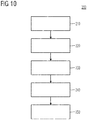
- Fig. 10 schematically and exemplarily illustrates a flow diagram of a method 200 of processing a wafer 100 (cf. Fig. 4 ), the method 200 including automatically the wafer 100, in accordance with one or more embodiments.
- processing the wafer 100 may refer to processing steps concerning the production of the wafer itself, or to processing steps regarding subsequent further processing of the wafer in terms of, e.g., forming microelectronic components, such as power semiconductor dies, Integrated Circuits (ICs), micromechanical systems (MEMS), photoelectric components thereon.
- processing the wafer 100 can designate a processing method applied for forming the plurality of microelectronic components 120 on/within the wafer 100, e.g., as shown in Fig. 4 .
- Such processing steps can be related to deposition, removal, patterning, or modification of electrical properties of the wafer 100.
- processing the wafer 100 may designate one, more or all processing steps of a processing chain that is executed for completely forming the microelectronic components (e.g., the power semiconductor dies, ICs, MEMS, photovoltaic devices etc.) 120 on/within the wafer 100.
- microelectronic components e.g., the power semiconductor dies, ICs, MEMS, photovoltaic devices etc.
- processing the wafer 100 can designate a processing method directed only to manufacturing the wafer 100 itself, independently from the later use of the wafer 100.
- processing the wafer may refer to a method of producing a carrier wafer or a product wafer or a wafer stack.
- the wafer 100 can for example be one of a semiconductor wafer, or a glass wafer or a plastic wafer.
- the wafer 100 can have a diameter e.g. of "6 inch”, “8 inch”, “12 inch” or “16 inch", to give a few examples.
- Automatically analyzing the wafer 100 comprises several steps, which will now be described with additional reference to Figs. 5, 6 and 7 .
- step 210 includes effecting 210 a relative movement between the wafer 100 and a camera device 310.
- Such relative movement may be effected by moving only the wafer 100 and maintaining the camera device 310 stationary.
- the relative movement between the wafer 100 and the camera device 310 is effected by a wafer aligner device 330 (cf. Fig. 7 ) used for the purpose of processing the wafer 100.
- the relative movement may be a linear movement of the wafer 100 or a rotational movement of the wafer 100.
- a velocity of the wafer movement may be within the range of 0,001 m/s to 100 m/s (in case of a linear movement), or within the range of 0,01 rpm to 1000 rpm (in case of a rotational movement).
- the camera device 310 may be digital camera device, e.g., a commercially available off-the-shelve camera device.
- the camera device 310 may operate by repeatly capturing images of the moving wafer 100, e.g., at a sampling rate of 1 - 1000 images per second, and at an image capture time t within the range of 0,001 ms to 100 ms for each image, and outputting corresponding receipt image data. Recording the images may require the image capture time t for each image. At least one of the sampling rate and the image capture time t may be adjustable.
- the camera device 310 may be positioned at a distance to the wafer 100 so as to be capable of obtaining image data in sufficient quality, e.g., a distance within 0,01 cm to 5 cm, or within 0,1 cm to 100 cm. A distance that may be appropriate for some embodiments amounts to about 3 cm.
- Step 220 which may be carried out simultaneously with step 210 (i.e., during relative movement between the wafer 100 and the camera device 310), includes subjecting the wafer 100 to a light emitted by a light source 320, in accordance with an embodiment.
- the light source 320 emits the light with a reference light pattern.
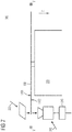
- Two exemplary light patterns A, B are illustrated in Fig. 6 .
- the reference light pattern can be for example one of a stripe pattern 81 and a checkerboard pattern 82.
- a maximum pitch P of the reference light pattern 81; 82 is adapted to the image capture time t of the camera device 310. E.g., a smaller pitch P may require a shorter image capture time t.
- the light source 320 For emitting light with the reference light pattern, in one embodiment, the light source 320 produces homogenous light that passes through a mask (not illustrated) before reaching the wafer 100, wherein the mask effects the reference light pattern.
- the light source 320 may comprise a controllable light panel, such as a controllable LED panel, and the light source 320 may be configured to output the light with the reference light pattern based on correspondingly controlling the light panel.
- the light source 320 emits light within the visual spectrum or within the infrared spectrum.
- light sources with higher frequencies can be used e.g. UV light sources.
- the light emitted by the light source 320 penetrates the moving wafer 100.
- the light emitted by the light source 320 may enter the wafer 100 at the wafer back surface 1102 and leave the wafer 100 at the wafer front surface 1101, or vice versa.
- the wafer surfaces 1101 and 1102 may be orientated substantially perpendicular to the light emission direction (as indicated by the vertical arrows in Fig. 5 ).
- a non-illustrated additional light source that directs additional light onto the wafer front surface 1101 such that the additional light is reflected by the wafer front surface 1101 and thereafter captured by the camera device 310.
- the wafer movement v may occur in a direction substantially perpendicular to the light emission direction of the light emitted by the light source 320 (as indicated by the vertical arrows in Fig. 5 ).
- the wafer 100 is moved between the camera device 310 and the light source 320.
- Both the camera device 310 and the light source 320 may be installed stationary, e.g., in a manner that the light source 320 emits the light towards the camera device 310, wherein the emitted light passes though the moving wafer 100 before reaching the camera device 310.
- the camera device 310 uses transmitted light (instead or in addition to light reflected by the wafer 100 (as in Fig. 2 )) for generating the image data.
- emission of the light with the reference light pattern is indicated by means of the bold and dotted arrows.
- the emitted light may exhibit the reference light pattern, such as the stripe pattern 81, as schematically and exemplarily illustrated in Fig. 6 , e.g., a patterned change between minimum (dotted arrows) and maximum light emission (solid arrow).
- Such light then traverses the moving wafer 100. If the wafer 100 does not exhibit any damage, the reference light pattern is not disturbed, as schematically and exemplarily illustrated in the left and right portions of Fig. 5 . However, regarding for example the central portion of the wafer 100 where the wafer 100 exhibits the contamination 111, the reference light pattern is disturbed, yielding reception of a receipt light pattern at the camera device 310 different from the reference light pattern.
- the maximum length l of the wafer section captured by the camera device 310 may for example be adjusted according to the current camera device control (e.g., its optical focus/range) and/or the distance between the camera device 310 and the wafer 100.
- the image capture time t of the camera device 310 can be predetermined or adjustable, depending of the type of the camera device 310.
- the velocity v can for example be controlled by correspondingly setting the means effecting the velocity.
- Such means may for example include the aligner device 330 as schematically shown in Fig. 7 , where the movement is a rotational movement indicated by the arrow head and the arrow foot.
- condition (1) it is for example possible to ensure that the section of the wafer 100 having length l and currently being recorded by the camera device 310 is sufficiently illuminated (in terms of total illumination time) by the light source 320. Further, it can be ensured that only one image is recorded for wafer section of length l . The next image is recorded for the subsequent wafer section of length l , wherein it can be ensured that there is neither an overlap between adjacent wafer sections nor a gap, in accordance with an embodiment.
- Step 230 includes generating, by the camera device 310 and based on the light that was emitted by the light source 320 and penetrated the moving wafer 100, receipt image data indicative for the receipt light pattern.
- step 230 may include continuously recording images, at the image sampling rate and with the image capture time t for each image, of the illuminated moving wafer 100 and providing the corresponding receipt image data.
- a processing unit 340 can be connected to the camera unit 310 and configured to receive the receipt image data from the camera unit 310.
- the processing unit 340 and the camera unit 310 may be integral parts of a camera apparatus.
- step 240 a difference between the reference light pattern and the receipt light pattern is determined, based on the receipt image data and reference image data.
- this difference is determined for each recorded image.
- the receipt image data may be subjected to a noise cancellation algorithm. Further, before the difference is determined, the receipt image data may be subjected to an edge cancellation algorithm for filtering out deviations caused by an edge of the wafer. The difference which is thereafter (after applying the noise and edge cancellation algorithms) determined may then be indicative for eventual wafer damages.
- the noise cancellation algorithm can for example be based on a Gaussian filter or on a non-linear filter, such as a median filter.
- Applying the edge cancellation algorithm may be appropriate if the recorded wafer section includes an image of an edge of the wafer 100.
- the edge of the wafer 100 i.e., the substantially vertically extending termination between the two wafer surfaces 1101 and 1102, may break the light irregularly and could thereby falsely indicate a wafer damage.
- the edge cancellation algorithm is based on thresholding, which is a known image processing technique regarding segmentation.
- the reference image data can be indicative of the reference light pattern.
- the reference image data can be produced based on averaged receipt image data obtained during previous measurements. For example, within the scope of these measurements, a damage-free wafer is used as a reference.
- Determining the difference between the reference light pattern and the receipt light pattern based on the receipt image data and reference image data may for example include, e.g., after pre-processing the receipt image data by subjecting the receipt image data to the noise and/or edge cancellation algorithm, forming a difference between the reference image data and the (pre-processed) receipt image data and, e.g., by applying one or more standard algorithms, like segmentation algorithms, e.g., a watershed image processing algorithm, a livewire image processing algorithm, or a region growing image processing algorithm.
- segmentation algorithms e.g., a watershed image processing algorithm, a livewire image processing algorithm, or a region growing image processing algorithm.
- Automatically analyzing the wafer 100 within the scope of processing the wafer 100 includes determining, in step 250, by the processing unit 340 and based on the difference between the reference light pattern and the receipt light pattern, a quality parameter that is indicative for a material character of the wafer 100.
- the quality parameter can be a binary parameter, a first value of which indicating presence of a wafer damage, a second value of which indicating absence of a wafer damage.
- the quality parameter may be more distinguished.
- the determining step 250 is primarily carried out so as to determine whether the wafer 100 is free of damages, i.e., fulfills a quality criterion and may hence be further processed, or whether the wafer 100 has a damage that disqualifies wafer 100 from being eventually shipped out to the customer.
- the determining step 240 and the determining step 250 may be carried out so as to classify the type of damage and/or so as to localize the damage.
- a corresponding quality parameter would then be output by the processing unit 340, indicating type and/or position of the damage.
- it may be appropriate to change the reference light pattern periodically during the image capturing.
- determining, in step 250, the quality parameter indicative for the material character of the wafer 100 may include carrying out at least one of an edge oriented segmentation algorithm or region orientated segmentation algorithm for gathering pixels of the receipt image data to components and/or a classification algorithm.
- an edge oriented segmentation algorithm or region orientated segmentation algorithm for gathering pixels of the receipt image data to components and/or a classification algorithm.
- standard image processing algorithms may be employed.
- the method 200 of processing the wafer 100 not only includes automatically analyzing the wafer 100, e.g., in a manner as exemplarily described above, but also controlling the processing of the wafer 100 based on the quality parameter. For example, if the quality parameter indicates that the wafer 100 is damaged, the process may be organized such that the damaged wafer is sorted out and not further processed.
- automatically analyzing the wafer 100 may occur during processing of the wafer 100.
- automatically analyzing the wafer 100 occurs during a deposition processing step, a removal processing step, a patterning processing step, or during a processing step related to the modification of electrical properties of the wafer 100.
- automatically analyzing the wafer 100 may occur between two processing steps, i.e., as a separate immediate processing step after the first processing step has been finished and before a subsequent processing step is started.
- Figs. 7 , 8 and 9 are schematically illustrated in Figs. 7 , 8 and 9 .
- the system 300 may be configured to carry out the process, entirely or at least partially, used for forming the microelectronic components 120 on/within the wafer 100.
- the system 300 may comprise the non-illustrated means for carrying out the deposition processing step(s), the removal processing step(s), the patterning processing step(s), and/or the processing step(s) related to the modification of electrical properties of the wafer 100.
- the system 300 is a system for wafer manufacturing, only, independent of the later use of the wafer, e.g., as a carrier wafer, a product wafer, a wafer stack, e.g., independent of what type of components (ICs, power semiconductor dies, MEMS, photovoltaic, etc.) are later implemented on/within the wafer 100.
- a carrier wafer e.g., as a carrier wafer, a product wafer, a wafer stack, e.g., independent of what type of components (ICs, power semiconductor dies, MEMS, photovoltaic, etc.) are later implemented on/within the wafer 100.
- a wafer stack e.g., independent of what type of components (ICs, power semiconductor dies, MEMS, photovoltaic, etc.) are later implemented on/within the wafer 100.
- processing steps 300-1, 300-2, 300-3 are illustrated, each of which is carried out by the system 300.
- Each of the processing steps 300-1, 300-2 and 300-3 can implement one of a deposition processing step, a removal processing step, a patterning processing step, and/or a processing step(s) related to the modification of electrical properties of the wafer 100.
- Subsequent steps, such as testing, preparation, packaging and the like may be carried out by one or more other systems receiving the wafer 100 processed by the system 300.
- the system 300 includes an apparatus for automatically analyzing the wafer 100, wherein the apparatus comprises: a camera device, a light source, a processing unit, and means for effecting a relative movement between the wafer and the camera device and so as to subject, during the relative movement between the wafer and the camera device, the wafer to a light emitted by the light source, wherein the light source emits the light with a reference light pattern, and wherein the emitted light penetrates the moving wafer.
- the camera device is configured to generate, based on the light that was emitted by the light source and penetrated the moving wafer, receipt image data indicative for a receipt light pattern.
- the processing unit is configured to determine a difference between the reference light pattern and the receipt light pattern based on the receipt image data and reference image data.
- the processing unit is configured to determine, based on the difference, a quality parameter indicative for a material character of the wafer.
- exemplary embodiments of the system 300 and its apparatus for automatically analyzing the wafer 100 it is fully referred to above described embodiments of the method 200 and the components that may be employed for carrying out the method 200.
- exemplary embodiments of the system 300 and its apparatus correspond to the exemplary embodiments of the method 200.
- system 300 is configured to carry out one or more of the above described embodiments of the method 200.
- FIGs. 8 and 9 two variants of including the apparatus within the system 300 shall be explained.
- the apparatus is included in the system 300 such that both the processing step 300-2 applied to the wafer 100 and automatically analyzing the wafer 100, e.g., in accordance with method 200, may occur simultaneously.
- performing the automatic analysis of the wafer 100 does not increase the total processing time needed for processing the wafer 100 by the system 300.
- the wafer 100 may be subjected to the subsequent processing step 300-3.
- the wafer 100 may be sorted out and, for example, be subjected to a separate processing step 300-10, where, for example, further measurements and/or inspections may be made.
- the apparatus is included in the system 300 such that automatically analyzing the wafer 100, e.g., in accordance with method 200, occurs within a separate processing step, e.g., after processing step 300-2 is completed and before the wafer 100 is subjected to processing steps 300-3 starts.
- a separate processing step e.g., after processing step 300-2 is completed and before the wafer 100 is subjected to processing steps 300-3 starts.
- the wafer 100 may be subjected to the subsequent processing step 300-3.
- the wafer 100 may be sorted out and, for example, be subjected to the separate processing step 300-10, where, for example, further measurements and/or inspections may be made.
- integration of the apparatus within an existing processing chain of a wafer production/processing plant can be possible without changing the process flow of the processing chain.
- multiple integration of wafer damage analysis apparatuses is possible; e.g., the wafer damage analysis may occur serval times at different processing steps of the process chain.
- these wafers are semiconductor substrates, i.e., the wafer 100 can be based on silicon (Si). Accordingly, a monocrystalline semiconductor region or layer can be a monocrystalline Si-region or Si-layer. In other embodiments, polycrystalline or amorphous silicon may be employed.
- the wafer 100 can be made of any semiconductor material.
- semiconductor materials include, without being limited thereto, elementary semiconductor materials such as silicon (Si) or germanium (Ge), group IV compound semiconductor materials such as silicon carbide (SiC) or silicon germanium (SiGe), binary, ternary or quaternary III-V semiconductor materials such as gallium nitride (GaN), gallium arsenide (GaAs), gallium phosphide (GaP), indium phosphide (InP), indium gallium phosphide (InGaPa), aluminum gallium nitride (AIGaN), aluminum indium nitride (AlInN), indium gallium nitride (InGaN), aluminum gallium indium nitride (AIGalnN) or indium gallium arsenide phosphide (InGaAsP), and binary or ternary II-VI semiconductor materials such as cadmium telluri
- heterojunction semiconductor materials include, without being limited thereto, aluminum gallium nitride (AIGaN)-aluminum gallium indium nitride (AIGalnN), indium gallium nitride (InGaN)-aluminum gallium indium nitride (AIGalnN), indium gallium nitride (InGaN)-gallium nitride (GaN), aluminum gallium nitride (AIGaN)-gallium nitride (GaN), indium gallium nitride (InGaN)-aluminum gallium nitride (AIGaN), silicon-silicon carbide (SixC1-x) and silicon-SiGe heterojunction semiconductor materials.
- InGaN aluminum gallium nitride
Landscapes
- Physics & Mathematics (AREA)
- Engineering & Computer Science (AREA)
- General Physics & Mathematics (AREA)
- Chemical & Material Sciences (AREA)
- Health & Medical Sciences (AREA)
- Life Sciences & Earth Sciences (AREA)
- Analytical Chemistry (AREA)
- Biochemistry (AREA)
- General Health & Medical Sciences (AREA)
- Immunology (AREA)
- Pathology (AREA)
- Computer Vision & Pattern Recognition (AREA)
- Theoretical Computer Science (AREA)
- Quality & Reliability (AREA)
- Testing Or Measuring Of Semiconductors Or The Like (AREA)
- Investigating Materials By The Use Of Optical Means Adapted For Particular Applications (AREA)
Abstract
Description
- This specification refers to embodiments of a method of processing a wafer, wherein the method includes automatically analyzing the wafer. This specification further refers to embodiments of a system of processing a wafer, wherein the system includes an apparatus for automatically analyzing the wafer. This specification also refers to embodiments of an apparatus for automatically analyzing a wafer.
- Many functions of modern devices in automotive, consumer and industrial applications, such as converting electrical energy and driving an electric motor or an electric machine, rely on power semiconductor devices. For example, power semiconductor devices, such as Insulated Gate Bipolar Transistors (IGBTs) and Metal Oxide Semiconductor Field Effect Transistors (MOSFETs) and diodes, have been used for various applications including, but not limited to switches in power supplies and power converters. Different kind of semiconductor technologies, such as CMOS (Complementary metal-oxide-semiconductor) technology, Bipolar technology, or a combination thereof, known as BiCMOS technology, may be applied for forming power semiconductor devices.
- Power semiconductor devices are typically processed on/within a wafer. After having been processed, the wafer is typically diced into a plurality of separate power semiconductor dies. Damages of a power semiconductor die can lead to a functional deficiency of the power semiconductor die itself and, eventually, to a malfunction or a failure of the of the power semiconductor device (including one or more of such dies) or even of the application in which the respective power semiconductor device is used.
- However, wafers not only serve as a basis for manufacturing power semiconductor dies, but for example also for manufacturing Integrated Circuits (ICs), microelectromechanical systems (MEMS), photoelectric components etc. Also in this context, the wafer should certainly be free of damages.
- Also, further processing of damaged wafers may harm tools that are employed for the further processing.
- Therefore, it may be desirable to reliably detect a damaged wafer and to control further processing accordingly.
- The subject-matter of the independent claims is presented. The dependent claims define features of exemplary embodiments.
- Aspects described herein relate to embedding a fully automatic wafer damage inspection, herein also referred to as wafer damage analysis, into the process chain of a wafer processing plant or a wafer production plant.
- Embedding the wafer damage analysis within the process chain may for example occur by providing a separate analysis step somewhere between the first and the last processing step the wafer passes through.
- Another variant is implementing the wafer damage analysis during one of the plurality of processing steps, e.g., simultaneously with at least one of a deposition processing step, a lithographic processing step, a wet processing step, an implantation processing step, an etch processing step, or simultaneously with any processing step related to deposition, removal, patterning, or modification of electrical properties of the wafer. For example, thereby, the throughput rate of the processing chain can be maintained; i.e., the wafer damage analysis may occur automatically without loss of time, e.g., in real-time with respect to the processing speed of the processing chain.
- Regarding implementation of the automatic analysis, it is for example proposed to emit light with a reference light pattern that traverses the moving wafer. The light that has traversed the moving wafer, and, optionally, additional light that has been reflected by the wafer, is received and compared with a reference. An eventual difference can be indicative of a damage within the wafer.
- According to an embodiment, a method of processing a wafer is presented. The method includes automatically analyzing the wafer, wherein automatically analyzing the wafer comprises: effecting a relative movement between the wafer and a camera device; during the relative movement between the wafer and the camera device: subjecting the wafer to a light emitted by a light source, wherein the light source emits the light with a reference light pattern; and the emitted light penetrates the moving wafer; generating, by the camera device and based on the light that was emitted by the light source and penetrated the moving wafer, receipt image data indicative for a receipt light pattern; determining, by a processing unit, a difference between the reference light pattern and the receipt light pattern based on the receipt image data and reference image data; determining, by the processing unit and based on the difference, a quality parameter indicative for a material character of the wafer.
- According to another embodiment, a system for processing a wafer is presented. The system includes an apparatus for automatically analyzing the wafer, wherein the apparatus comprises: a camera device, a light source, a processing unit, and means for effecting a relative movement between the wafer and the camera device and so as to subject, during the relative movement between the wafer and the camera device, the wafer to a light emitted by the light source, wherein the light source emits the light with a reference light pattern, and wherein the emitted light penetrates the moving wafer; wherein: the camera device is configured to generate, based on the light that was emitted by the light source and penetrated the moving wafer, receipt image data indicative for a receipt light pattern; the processing unit is configured to determine a difference between the reference light pattern and the receipt light pattern based on the receipt image data and reference image data; the processing unit is configured to determine, based on the difference, a quality parameter indicative for a material character of the wafer.
- According to a yet further embodiment, an apparatus for automatically analyzing a wafer is presented. The apparatus comprises: a camera device, a light source, a processing unit, and means for effecting a relative movement between the wafer and the camera device and so as to subject, during the relative movement between the wafer and the camera device, the wafer to a light emitted by the light source, wherein the light source emits the light with a reference light pattern, and wherein the emitted light penetrates the moving wafer; wherein: the camera device is configured to generate, based on the light that was emitted by the light source and penetrated the moving wafer, receipt image data indicative for a receipt light pattern; the processing unit is configured to determine a difference between the reference light pattern and the receipt light pattern based on the receipt image data and reference image data; and the processing unit is configured to determine, based on the difference, a quality parameter indicative for a material character of the wafer.
- Within the scope of the present specification, the term "wafer" has the meaning the skilled person typically associates therewith.
- For example, the wafer can be a product wafer, e.g., a wafer serving as a basis for manufacturing microelectronic components, such as power semiconductor dies, Integrated Circuits (ICs), micromechanical systems (MEMS), photoelectric components etc. Such wafer may also be referred to as "substrate". For example, the wafer is a semiconductor wafer (also referred to as semiconductor substrate).
- In another example, the wafer is a carrier wafer. E.g., a carrier wafer may be used as an auxiliary wafer for processing thin semiconductor wafers. Also such type of wafer may also be referred to as "substrate". Carrier wafers are for example used to permit the safe handling of sensitive semiconductor wafers (e.g. those made of silicon and gallium arsenide). For example, the carrier wafer can be a glass wafer, a plastic wafer, or a semiconductor wafer.
- In yet another example, the wafer is or forms a part of a wafer stack of two or more wafers that are, e.g., bonded to each other, e.g., for forming three-dimensional integrated circuits thereon (e.g. applying a technology referred to as TSV (through silicon via)). For example, the wafer can be a glass on silicon wafer, or a silicon on glass wafer. Also such wafer type may be referred to as substrate or, respectively, substrate stack.
- Generally, the herein described embodiments are suited for analyzing arbitrary wafer types. It is pointed out the above mentioned wafer types may also be referred to as substrates. The material of the wafer being processed/analyzed (e.g., the substrate being processed/analyzed) may be a semiconductor material (e.g., Si, GaN, SiC, to name a few), a glass, or a plastic material.
- As used herein, the term "processing the wafer" may refer to processing steps concerning the production of the wafer itself, or to processing steps regarding subsequent further processing of the wafer in terms of, e.g., forming microelectronic components thereon, such as power semiconductor dies, Integrated Circuits (ICs), micromechanical systems (MEMS), photoelectric components, etc..
- Those skilled in the art will recognize additional features and advantages upon reading the following detailed description, and upon viewing the accompanying drawings.
- The parts in the figures are not necessarily to scale, instead emphasis being placed upon illustrating principles of the invention. Moreover, in the figures, like reference numerals may designate corresponding parts. In the drawings:
- Fig. 1
- schematically and exemplarily illustrates a section of a vertical cross-section of a wafer;
- Fig. 2
- schematically and exemplarily illustrates a method of analyzing a wafer;
- Fig. 3
- schematically and exemplarily illustrates another method of analyzing a wafer;
- Fig. 4
- schematically and exemplarily illustrates a horizontal projection of a wafer having a plurality of components implemented thereon, in accordance with one or more embodiments;
- Fig. 5
- schematically and exemplarily illustrates a method of processing a wafer, the method including automatically analyzing the wafer, in accordance with one or more embodiments;
- Fig. 6
- schematically and exemplarily illustrates two variants of a reference light pattern that may be employed for automatically analyzing a wafer, in accordance with one or more embodiments;
- Fig. 7
- schematically and exemplarily illustrates a section of a system for processing a wafer, the system including an apparatus for automatically analyzing the wafer, in accordance with one or more embodiments;
- Fig. 8
- schematically and exemplarily illustrates a section of a system for processing a wafer, the system including an apparatus for automatically analyzing the wafer, in accordance with one or more embodiments;
- Fig. 9
- schematically and exemplarily illustrates a section of a system for processing a wafer, the system including an apparatus for automatically analyzing the wafer, in accordance with one or more embodiments; and
- Fig. 10
- schematically and exemplarily illustrates a flow diagram of a method of processing a wafer, the method including automatically analyzing the wafer, in accordance with one or more embodiments.
- In the following detailed description, reference is made to the accompanying drawings which form a part hereof and in which are shown by way of illustration specific embodiments in which the invention may be practiced.
- In this regard, directional terminology, such as "top", "bottom", "below", "front", "behind", "back", "leading", "trailing", "above" etc., may be used with reference to the orientation of the figures being described. Because parts of embodiments can be positioned in a number of different orientations, the directional terminology is used for purposes of illustration and is in no way limiting. It is to be understood that other embodiments may be utilized and structural or logical changes may be made without departing from the scope of the present invention. The following detailed description, therefore, is not to be taken in a limiting sense, and the scope of the present invention is defined by the appended claims.
- Reference will now be made in detail to various embodiments, one or more examples of which are illustrated in the figures. Each example is provided by way of explanation, and is not meant as a limitation of the invention. For example, features illustrated or described as part of one embodiment can be used on or in conjunction with other embodiments to yield yet a further embodiment. It is intended that the present invention includes such modifications and variations. The examples are described using specific language which should not be construed as limiting the scope of the appended claims. The drawings are not scaled and are for illustrative purposes only. For clarity, the same elements or manufacturing steps have been designated by the same references in the different drawings if not stated otherwise.
- The term "horizontal" as used in this specification intends to describe an orientation substantially parallel to a horizontal surface. This can be for instance the surface of a wafer. For example, both the first lateral direction X and the second lateral direction Y mentioned below can be horizontal directions, wherein the first lateral direction X and the second lateral direction Y may be perpendicular to each other.
- The term "vertical" as used in this specification intends to describe an orientation which is substantially arranged perpendicular to the horizontal surface, i.e., parallel to the normal direction of the surface of the substrate/wafer. For example, the extension direction Z mentioned below may be an extension direction that is perpendicular to both the first lateral direction X and the second lateral direction Y. The extension direction Z is also referred to as "vertical direction Z" herein.
- Some exemplary embodiments described in this specification are related to, without being limited thereto, power semiconductor devices, e.g., power semiconductor devices that may be used within a power converter or a power supply. Thus, in an embodiment, such devices can be configured to carry a load current that is to be fed to a load and/or, respectively, that is provided by a power source. For example, the power semiconductor devices may comprise one or more active power semiconductor dies each having one or more active power semiconductor cells, such as a monolithically integrated diode cell, e.g., monolithically integrated cell of two anti-serially connected diodes, a monolithically integrated transistor cell, e.g., a monolithically integrated IGBT cell, a monolithically integrated MOSFET cell and/or derivatives thereof. Such diode/transistor cells may be integrated in an active region (cell field) of a power semiconductor die, which may then be integrated in a power semiconductor device.
- The term "power semiconductor die" as used in this specification intends to describe a single power semiconductor chip with high voltage blocking and/or high current-carrying capabilities. In other words, such power semiconductor die is intended for high current, typically in the Ampere range, e.g., up to several ten or hundred Ampere, and/or high voltages, typically above 15 V, more typically 100 V and above, e.g., up to at least 400 V or even more, e.g., up to at least 3 kV.
- A plurality of power semiconductor dies may be processed simultaneously on a wafer. After the plurality of power semiconductor dies have been processed on the wafer, the wafer may be subjected to a dicing step, during which the wafer is diced into the plurality of separate power semiconductor dies. A singular one of these dies or a plurality of these dies may then be integrated within a package, e.g., so as to form the power semiconductor device.
- However, as also mentioned introductorily, wafers not only serve as a basis for manufacturing power semiconductor dies, but also for manufacturing other microelectronic components, such as Integrated Circuits (ICs), micromechanical systems (MEMS), photoelectric components etc.
- It is usually desirable to guarantee correct functionality of the microelectronic components that are shipped out to the customer. To this end, checks/analyses/inspections may be carried out before, during and/or after the processing so as to ensure that functionally working and non-damaged components are shipped out.
- The present specification is generally directed to manufacturing or processing a wafer of an arbitrary type, wherein manufacturing or processing the wafer includes an embedded analysis of the wafer. The wafer manufactured may for example be further processed by forming microelectronic components, such as power semiconductor dies, ICs, MEMS, photovoltaic devices and the like thereon. As mentioned introductorily, the wafer can be of any type, e.g., a glass wafer, a semiconductor wafer, a plastic wafer and so on. The wafer may even be based on several substrates, such as silicon-on-glass arrangements and so on.
- Regarding possible damages of the wafer, it is referred to
Fig. 1 , which schematically and exemplarily illustrates a section of a vertical cross-section of thewafer 100. - For example, a first type of a damage of the
wafer 100 can be acontamination 111 on afront surface 1101 and/or on aback surface 1102 of thewafer 100. Such contamination can also be within thewafer 100. - Another type of damage that may additionally or alternatively occur is an
inclusion 112 within thewafer 100. - Another type of damage that may additionally or alternatively occur is a
crack 113 extending (e.g., from one of thefront surface 1101 and the back surface 1102) into thewafer 100. - Yet another type of damage that may additionally or alternatively occur is an eruption or groove 114 of the
wafer 100. - The aforementioned exemplary types of damages of the
wafer 100 may lead to performance degradation or even malfunction of the components to be formed on/within thewafer 100. - Moreover, the damages may lead to performance degradation or even malfunction of a processing tool of the production plant currently processing the wafer. Hence, if a wafer having a damage is not detected (and, e.g., not accordingly sorted out) further processing of the damaged wafer may cause significant reduction of the throughput rate of the production plant.
- For example, referring to
Fig. 4 , which schematically and exemplarily illustrates a horizontal projection of thewafer 100, a plurality ofmicroelectronic components 120, such as power semiconductor dies or other components (ICs, MEMs, ...) may be formed on/within thewafer 100, namely by applying typical device fabrication processing steps. Such processing steps can be related to deposition, removal, patterning, or modification of electrical properties of thewafer 100. - According to the aforesaid, the processing steps may not yield the desired effects if the
wafer 100 exhibits damages, e.g., those as exemplarily described with respect toFig. 1 . Or, applying the processing steps may cause wafer damages, e.g., those as exemplarily described with respect toFig. 1 . - Hence, it is desirable to determine presence or non-presence of
such damages wafer 100 based on the determination. - For example, with reference to
Fig. 2 , to make this determination, it is possible to direct light L in a tilted (with respect to the vertical direction Z) manner onto thesurface 1101 of thewafer 100 and to analyze, by means of a camera, theimage 50 that was obtained based on the reflected light L'. E.g., by applying image processing algorithms, the presence of thecontamination 111 may be determined based on detecting a corresponding image portion 111' in theimage 50, and presence of thecrack 113 may be determined by detecting a corresponding image portion 113' in theimage 50. - Another option, as schematically and exemplarily illustrated in
Fig. 3 , is to direct the light L through thewafer 100, i.e., such that it penetrates theback surface 1102 and thefront surface 1101 and to analyze this light. E.g., thereby, presence of the eruption/groove 114 may be determined. - Aspects described herein relate to improving the determination of the presence of one or more wafer damages (such as the
damages wafer 100, wherein the damage analysis is embedded in said processing chain. For example, the embedded damage analysis not only allows efficient detection of a damaged wafer, but also the prevention of further processing of a damaged wafer (that, e.g., could damage a processing tool employed during the wafer processing). -
Fig. 10 schematically and exemplarily illustrates a flow diagram of amethod 200 of processing a wafer 100 (cf.Fig. 4 ), themethod 200 including automatically thewafer 100, in accordance with one or more embodiments. - As indicated above, the term "processing the
wafer 100" may refer to processing steps concerning the production of the wafer itself, or to processing steps regarding subsequent further processing of the wafer in terms of, e.g., forming microelectronic components, such as power semiconductor dies, Integrated Circuits (ICs), micromechanical systems (MEMS), photoelectric components thereon. E.g., "processing thewafer 100" can designate a processing method applied for forming the plurality ofmicroelectronic components 120 on/within thewafer 100, e.g., as shown inFig. 4 . Such processing steps can be related to deposition, removal, patterning, or modification of electrical properties of thewafer 100. Hence, as used herein "processing thewafer 100" may designate one, more or all processing steps of a processing chain that is executed for completely forming the microelectronic components (e.g., the power semiconductor dies, ICs, MEMS, photovoltaic devices etc.) 120 on/within thewafer 100. - In other embodiments, "processing the
wafer 100" can designate a processing method directed only to manufacturing thewafer 100 itself, independently from the later use of thewafer 100. E.g., "processing the wafer" may refer to a method of producing a carrier wafer or a product wafer or a wafer stack. - As explained above, the
wafer 100 can for example be one of a semiconductor wafer, or a glass wafer or a plastic wafer. Thewafer 100 can have a diameter e.g. of "6 inch", "8 inch", "12 inch" or "16 inch", to give a few examples. - Automatically analyzing the
wafer 100 comprises several steps, which will now be described with additional reference toFigs. 5, 6 and7 . - For example,
step 210 includes effecting 210 a relative movement between thewafer 100 and acamera device 310. Such relative movement may be effected by moving only thewafer 100 and maintaining thecamera device 310 stationary. For example, the relative movement between thewafer 100 and thecamera device 310 is effected by a wafer aligner device 330 (cf.Fig. 7 ) used for the purpose of processing thewafer 100. - The relative movement may be a linear movement of the
wafer 100 or a rotational movement of thewafer 100. For example, a velocity of the wafer movement may be within the range of 0,001 m/s to 100 m/s (in case of a linear movement), or within the range of 0,01 rpm to 1000 rpm (in case of a rotational movement). - The
camera device 310 may be digital camera device, e.g., a commercially available off-the-shelve camera device. Thecamera device 310 may operate by repeatly capturing images of the movingwafer 100, e.g., at a sampling rate of 1 - 1000 images per second, and at an image capture time t within the range of 0,001 ms to 100 ms for each image, and outputting corresponding receipt image data. Recording the images may require the image capture time t for each image. At least one of the sampling rate and the image capture time t may be adjustable. - The
camera device 310 may be positioned at a distance to thewafer 100 so as to be capable of obtaining image data in sufficient quality, e.g., a distance within 0,01 cm to 5 cm, or within 0,1 cm to 100 cm. A distance that may be appropriate for some embodiments amounts to about 3 cm. -
Step 220, which may be carried out simultaneously with step 210 (i.e., during relative movement between thewafer 100 and the camera device 310), includes subjecting thewafer 100 to a light emitted by alight source 320, in accordance with an embodiment. - For example, the
light source 320 emits the light with a reference light pattern. Two exemplary light patterns A, B are illustrated inFig. 6 . Hence, the reference light pattern can be for example one of astripe pattern 81 and acheckerboard pattern 82. For example, a maximum pitch P of thereference light pattern 81; 82 is adapted to the image capture time t of thecamera device 310. E.g., a smaller pitch P may require a shorter image capture time t. - For emitting light with the reference light pattern, in one embodiment, the
light source 320 produces homogenous light that passes through a mask (not illustrated) before reaching thewafer 100, wherein the mask effects the reference light pattern. In another embodiment, thelight source 320 may comprise a controllable light panel, such as a controllable LED panel, and thelight source 320 may be configured to output the light with the reference light pattern based on correspondingly controlling the light panel. - For example, the
light source 320 emits light within the visual spectrum or within the infrared spectrum. For special purposes, even light sources with higher frequencies can be used e.g. UV light sources. - Still referring to step 220, and as more clearly illustrated in
Fig. 5 , the light emitted by thelight source 320 penetrates the movingwafer 100. For example, the light emitted by thelight source 320 may enter thewafer 100 at the wafer backsurface 1102 and leave thewafer 100 at thewafer front surface 1101, or vice versa. For example, thewafer surfaces Fig. 5 ). - In an embodiment, there may be provided a non-illustrated additional light source that directs additional light onto the
wafer front surface 1101 such that the additional light is reflected by thewafer front surface 1101 and thereafter captured by thecamera device 310. - In accordance with an embodiment, the wafer movement v may occur in a direction substantially perpendicular to the light emission direction of the light emitted by the light source 320 (as indicated by the vertical arrows in
Fig. 5 ). - For example, with respect to the light emission direction (as indicated by the vertical arrows in
Fig. 5 ), thewafer 100 is moved between thecamera device 310 and thelight source 320. Both thecamera device 310 and thelight source 320 may be installed stationary, e.g., in a manner that thelight source 320 emits the light towards thecamera device 310, wherein the emitted light passes though the movingwafer 100 before reaching thecamera device 310. - Hence, in an embodiment, the
camera device 310 uses transmitted light (instead or in addition to light reflected by the wafer 100 (as inFig. 2 )) for generating the image data. - In
Fig. 5 , emission of the light with the reference light pattern is indicated by means of the bold and dotted arrows. Hence, between the movingwafer 100 and thelight source 320, the emitted light may exhibit the reference light pattern, such as thestripe pattern 81, as schematically and exemplarily illustrated inFig. 6 , e.g., a patterned change between minimum (dotted arrows) and maximum light emission (solid arrow). Such light then traverses the movingwafer 100. If thewafer 100 does not exhibit any damage, the reference light pattern is not disturbed, as schematically and exemplarily illustrated in the left and right portions ofFig. 5 . However, regarding for example the central portion of thewafer 100 where thewafer 100 exhibits thecontamination 111, the reference light pattern is disturbed, yielding reception of a receipt light pattern at thecamera device 310 different from the reference light pattern. - Further, in an embodiment, the image capture time t of the
camera device 310, a maximum length l of a wafer section captured by thecamera device 310, and the velocity v of the relative movement are set to each other so as to fulfill the condition
- The maximum length l of the wafer section captured by the
camera device 310 may for example be adjusted according to the current camera device control (e.g., its optical focus/range) and/or the distance between thecamera device 310 and thewafer 100. - The image capture time t of the
camera device 310 can be predetermined or adjustable, depending of the type of thecamera device 310. - The velocity v can for example be controlled by correspondingly setting the means effecting the velocity. Such means may for example include the
aligner device 330 as schematically shown inFig. 7 , where the movement is a rotational movement indicated by the arrow head and the arrow foot. - By setting the parameters t, l and v so as to fulfill, at least substantially, condition (1), it is for example possible to ensure that the section of the
wafer 100 having length l and currently being recorded by thecamera device 310 is sufficiently illuminated (in terms of total illumination time) by thelight source 320. Further, it can be ensured that only one image is recorded for wafer section of length l. The next image is recorded for the subsequent wafer section of length l, wherein it can be ensured that there is neither an overlap between adjacent wafer sections nor a gap, in accordance with an embodiment. - Step 230 includes generating, by the
camera device 310 and based on the light that was emitted by thelight source 320 and penetrated the movingwafer 100, receipt image data indicative for the receipt light pattern. - For example, step 230 may include continuously recording images, at the image sampling rate and with the image capture time t for each image, of the illuminated moving
wafer 100 and providing the corresponding receipt image data. - A
processing unit 340 can be connected to thecamera unit 310 and configured to receive the receipt image data from thecamera unit 310. Of course, theprocessing unit 340 and thecamera unit 310 may be integral parts of a camera apparatus. - In
step 240, a difference between the reference light pattern and the receipt light pattern is determined, based on the receipt image data and reference image data. - For example, this difference is determined for each recorded image.
- Before the difference is determined, the receipt image data may be subjected to a noise cancellation algorithm. Further, before the difference is determined, the receipt image data may be subjected to an edge cancellation algorithm for filtering out deviations caused by an edge of the wafer. The difference which is thereafter (after applying the noise and edge cancellation algorithms) determined may then be indicative for eventual wafer damages.
- The noise cancellation algorithm can for example be based on a Gaussian filter or on a non-linear filter, such as a median filter.
- Applying the edge cancellation algorithm may be appropriate if the recorded wafer section includes an image of an edge of the
wafer 100. The edge of thewafer 100, i.e., the substantially vertically extending termination between the twowafer surfaces - The reference image data can be indicative of the reference light pattern. In an embodiment, the reference image data can be produced based on averaged receipt image data obtained during previous measurements. For example, within the scope of these measurements, a damage-free wafer is used as a reference.
- Determining the difference between the reference light pattern and the receipt light pattern based on the receipt image data and reference image data may for example include, e.g., after pre-processing the receipt image data by subjecting the receipt image data to the noise and/or edge cancellation algorithm, forming a difference between the reference image data and the (pre-processed) receipt image data and, e.g., by applying one or more standard algorithms, like segmentation algorithms, e.g., a watershed image processing algorithm, a livewire image processing algorithm, or a region growing image processing algorithm.
- Automatically analyzing the
wafer 100 within the scope of processing thewafer 100 includes determining, instep 250, by theprocessing unit 340 and based on the difference between the reference light pattern and the receipt light pattern, a quality parameter that is indicative for a material character of thewafer 100. - In a simple form, the quality parameter can be a binary parameter, a first value of which indicating presence of a wafer damage, a second value of which indicating absence of a wafer damage.
- In other embodiments, the quality parameter may be more distinguished. However, the determining
step 250 is primarily carried out so as to determine whether thewafer 100 is free of damages, i.e., fulfills a quality criterion and may hence be further processed, or whether thewafer 100 has a damage that disqualifieswafer 100 from being eventually shipped out to the customer. - Nevertheless, further embodiments in this regard are conceivable. For example, the determining
step 240 and the determiningstep 250 may be carried out so as to classify the type of damage and/or so as to localize the damage. A corresponding quality parameter would then be output by theprocessing unit 340, indicating type and/or position of the damage. For example, in order to classify the type of damage and/or in order to localize the damage, it may be appropriate to change the reference light pattern periodically during the image capturing. - In an embodiment, determining, in
step 250, the quality parameter indicative for the material character of thewafer 100, may include carrying out at least one of an edge oriented segmentation algorithm or region orientated segmentation algorithm for gathering pixels of the receipt image data to components and/or a classification algorithm. Basically, for determining the quality parameter, standard image processing algorithms may be employed. - In accordance with an embodiment, the
method 200 of processing thewafer 100 not only includes automatically analyzing thewafer 100, e.g., in a manner as exemplarily described above, but also controlling the processing of thewafer 100 based on the quality parameter. For example, if the quality parameter indicates that thewafer 100 is damaged, the process may be organized such that the damaged wafer is sorted out and not further processed. - As has already been introductorily described, automatically analyzing the
wafer 100 may occur during processing of thewafer 100. For example, automatically analyzing thewafer 100 occurs during a deposition processing step, a removal processing step, a patterning processing step, or during a processing step related to the modification of electrical properties of thewafer 100. - In another embodiment, automatically analyzing the
wafer 100 may occur between two processing steps, i.e., as a separate immediate processing step after the first processing step has been finished and before a subsequent processing step is started. - Presented herein is also a system for processing a wafer. Exemplary embodiments are schematically illustrated in
Figs. 7 ,8 and 9 . - The
system 300 may be configured to carry out the process, entirely or at least partially, used for forming themicroelectronic components 120 on/within thewafer 100. Hence, thesystem 300 may comprise the non-illustrated means for carrying out the deposition processing step(s), the removal processing step(s), the patterning processing step(s), and/or the processing step(s) related to the modification of electrical properties of thewafer 100. In other embodiments, thesystem 300 is a system for wafer manufacturing, only, independent of the later use of the wafer, e.g., as a carrier wafer, a product wafer, a wafer stack, e.g., independent of what type of components (ICs, power semiconductor dies, MEMS, photovoltaic, etc.) are later implemented on/within thewafer 100. - For example, referring to
Figs. 8 and 9 , processing steps 300-1, 300-2, 300-3 are illustrated, each of which is carried out by thesystem 300. Each of the processing steps 300-1, 300-2 and 300-3 can implement one of a deposition processing step, a removal processing step, a patterning processing step, and/or a processing step(s) related to the modification of electrical properties of thewafer 100. - Subsequent steps, such as testing, preparation, packaging and the like may be carried out by one or more other systems receiving the
wafer 100 processed by thesystem 300. - The
system 300 includes an apparatus for automatically analyzing thewafer 100, wherein the apparatus comprises: a camera device, a light source, a processing unit, and means for effecting a relative movement between the wafer and the camera device and so as to subject, during the relative movement between the wafer and the camera device, the wafer to a light emitted by the light source, wherein the light source emits the light with a reference light pattern, and wherein the emitted light penetrates the moving wafer. The camera device is configured to generate, based on the light that was emitted by the light source and penetrated the moving wafer, receipt image data indicative for a receipt light pattern. The processing unit is configured to determine a difference between the reference light pattern and the receipt light pattern based on the receipt image data and reference image data. The processing unit is configured to determine, based on the difference, a quality parameter indicative for a material character of the wafer. - It is emphasized that, herein, the above described apparatus is not only presented as part of the
system 300, but also as an apparatus separate and independent of thesystem 300. - Regarding exemplary embodiments of the
system 300 and its apparatus for automatically analyzing thewafer 100, it is fully referred to above described embodiments of themethod 200 and the components that may be employed for carrying out themethod 200. Hence, exemplary embodiments of thesystem 300 and its apparatus correspond to the exemplary embodiments of themethod 200. - For example, the
system 300 is configured to carry out one or more of the above described embodiments of themethod 200. - Now referring to
Figs. 8 and 9 , two variants of including the apparatus within thesystem 300 shall be explained. - According to the embodiment illustrated in
Fig. 8 , the apparatus is included in thesystem 300 such that both the processing step 300-2 applied to thewafer 100 and automatically analyzing thewafer 100, e.g., in accordance withmethod 200, may occur simultaneously. Hence, performing the automatic analysis of thewafer 100 does not increase the total processing time needed for processing thewafer 100 by thesystem 300. For example, if the obtained quality parameter indicates that thewafer 100 is not damaged, thewafer 100 may be subjected to the subsequent processing step 300-3. If the obtained quality parameter indicates that thewafer 100 is damaged, thewafer 100 may be sorted out and, for example, be subjected to a separate processing step 300-10, where, for example, further measurements and/or inspections may be made. - According to the embodiment illustrated in
Fig. 9 , the apparatus is included in thesystem 300 such that automatically analyzing thewafer 100, e.g., in accordance withmethod 200, occurs within a separate processing step, e.g., after processing step 300-2 is completed and before thewafer 100 is subjected to processing steps 300-3 starts. Again, if for example the obtained quality parameter indicates that thewafer 100 is not damaged, thewafer 100 may be subjected to the subsequent processing step 300-3. If the obtained quality parameter indicates that thewafer 100 is damaged, thewafer 100 may be sorted out and, for example, be subjected to the separate processing step 300-10, where, for example, further measurements and/or inspections may be made. - Irrespective of whether the automatic analysis of the
wafer 100 is carried out during a processing step or in between two processing steps, manual inspection of thewafer 100 can be avoided, in accordance with an embodiment. Hence, the degree of automatization of thesystem 300 can be increased. Taking into account that further processing of a damaged wafer may even harm thesystem 300, the above described embodiments may even render the operation of thewafer processing system 300 more reliable and more efficient. - Further, integration of the apparatus within an existing processing chain of a wafer production/processing plant can be possible without changing the process flow of the processing chain. Also, multiple integration of wafer damage analysis apparatuses is possible; e.g., the wafer damage analysis may occur serval times at different processing steps of the process chain.
- In the above, embodiments pertaining to wafers, e.g., suited for forming power semiconductor devices, and corresponding processing methods were explained. For example, these wafers are semiconductor substrates, i.e., the
wafer 100 can be based on silicon (Si). Accordingly, a monocrystalline semiconductor region or layer can be a monocrystalline Si-region or Si-layer. In other embodiments, polycrystalline or amorphous silicon may be employed. - It should, however, be understood that the
wafer 100 can be made of any semiconductor material. Examples of such materials include, without being limited thereto, elementary semiconductor materials such as silicon (Si) or germanium (Ge), group IV compound semiconductor materials such as silicon carbide (SiC) or silicon germanium (SiGe), binary, ternary or quaternary III-V semiconductor materials such as gallium nitride (GaN), gallium arsenide (GaAs), gallium phosphide (GaP), indium phosphide (InP), indium gallium phosphide (InGaPa), aluminum gallium nitride (AIGaN), aluminum indium nitride (AlInN), indium gallium nitride (InGaN), aluminum gallium indium nitride (AIGalnN) or indium gallium arsenide phosphide (InGaAsP), and binary or ternary II-VI semiconductor materials such as cadmium telluride (CdTe) and mercury cadmium telluride (HgCdTe) to name few. The aforementioned semiconductor materials are also referred to as "homojunction semiconductor materials". When combining two different semiconductor materials a heterojunction semiconductor material is formed. Examples of heterojunction semiconductor materials include, without being limited thereto, aluminum gallium nitride (AIGaN)-aluminum gallium indium nitride (AIGalnN), indium gallium nitride (InGaN)-aluminum gallium indium nitride (AIGalnN), indium gallium nitride (InGaN)-gallium nitride (GaN), aluminum gallium nitride (AIGaN)-gallium nitride (GaN), indium gallium nitride (InGaN)-aluminum gallium nitride (AIGaN), silicon-silicon carbide (SixC1-x) and silicon-SiGe heterojunction semiconductor materials. For power semiconductor switch applications currently mainly Si, SiC, GaAs and GaN materials are used. - Spatially relative terms such as "under", "below", "lower", "over", "upper" and the like, are used for ease of description to explain the positioning of one element relative to a second element. These terms are intended to encompass different orientations of the respective device in addition to different orientations than those depicted in the figures. Further, terms such as "first", "second", and the like, are also used to describe various elements, regions, sections, etc. and are also not intended to be limiting. Like terms refer to like elements throughout the description.
- As used herein, the terms "having", "containing", "including", "comprising", "exhibiting" and the like are open ended terms that indicate the presence of stated elements or features, but do not preclude additional elements or features.
- With the above range of variations and applications in mind, it should be understood that the present invention is not limited by the foregoing description, nor is it limited by the accompanying drawings. Instead, the present invention is limited only by the following claims and their legal equivalents.
Claims (15)
- A method (200) of processing a wafer (100), the method (200) including automatically analyzing the wafer, wherein automatically analyzing the wafer (100) comprises:- effecting (210) a relative movement between the wafer (100) and a camera device (310);- during the relative movement between the wafer (100) and the camera device (310): subjecting (220) the wafer (100) to a light emitted by a light source (320), wherein- the light source (320) emits the light with a reference light pattern; and- the emitted light penetrates the moving wafer (100);- generating (230), by the camera device (310) and based on the light that was emitted by the light source (320) and penetrated the moving wafer (100), receipt image data indicative for a receipt light pattern;- determining (240), by a processing unit (340), a difference between the reference light pattern and the receipt light pattern based on the receipt image data and reference image data;- determining (250), by the processing unit (340) and based on the difference, a quality parameter indicative for a material character of the wafer (100).
- The method (200) of claim 1, further comprising controlling further processing of the wafer (100) based on the quality parameter.
- The method (200) of claim 1 or 2, wherein automatically analyzing the wafer (100) occurs during processing of the wafer (100).
- The method (200) of one of the preceding claims, wherein the quality parameter indicates presence or non-presence of at least one of the following:- a contamination (111) on a surface (1101, 1102) of the wafer (100) or within the wafer (100);- an inclusion (112) within the wafer (100);- a crack (113) extending into the wafer (100);- an eruption or groove (114) of the wafer (100).
- The method (200) of one of the preceding claims, wherein the reference light pattern is one of a stripe pattern (81) and a checkerboard pattern (82).
- The method (200) of one of the preceding claims, wherein a maximum pitch (P) of the reference light pattern is adapted to an image capture time of the camera device (310).
- The method (200) of one of the preceding claims, wherein the emitted light is within the visual spectrum or within the infrared spectrum or within the ultraviolet, UV, spectrum.
- The method (200) of one of the preceding claims, wherein the wafer (100) is one of the following: a semiconductor wafer, a glass wafer, a plastic wafer, or a wafer of a wafer stack.
- The method (200) of one of the preceding claims, wherein an image capture time t of the camera device (310), a maximum length l of a wafer section captured by the camera device (310), and a velocity v of the relative movement are set to each other so as to fulfill the condition t = l/v.
- The method (200) of one of the preceding claims, wherein, before determining (240) the difference between the reference light pattern and the receipt light pattern based on the receipt image data and the reference image data, at least one of the following is carried out:- subjecting the receipt image date to a noise cancellation algorithm; and- producing the reference image data based on averaged receipt image data obtained during previous measurements.
- The method (200) of one of the preceding claims, wherein determining (250) the quality parameter indicative for the material character of the wafer (100) includes carrying out at least one of:- a segmentation algorithm; and- a classification algorithm.
- The method (200) of one of the preceding claims, wherein the relative movement between the wafer (100) and the camera device (310) is effected by a wafer aligner device (330).
- The method (200) of one of the preceding claims, wherein the receipt image data is generated further based on light that was reflected by the wafer (100).
- A system (300) for processing a wafer (100), the system (300) including an apparatus for automatically analyzing the wafer (100), wherein the apparatus comprises:- a camera device (310), a light source (320), a processing unit (340), and means (330) for effecting a relative movement between the wafer (100) and the camera device (310) and so as to subject, during the relative movement between the wafer (100) and the camera device (310), the wafer (100) to a light emitted by the light source (320), wherein the light source (320) emits the light with a reference light pattern, and wherein the emitted light penetrates the moving wafer (100);wherein:- the camera device (310) is configured to generate, based on the light that was emitted by the light source (320) and penetrated the moving wafer (100), receipt image data indicative for a receipt light pattern;- the processing unit (340) is configured to determine a difference between the reference light pattern and the receipt light pattern based on the receipt image data and reference image data;- the processing unit (340) is configured to determine, based on the difference, a quality parameter indicative for a material character of the wafer (100).
- An apparatus for automatically analyzing a wafer (100), wherein the apparatus comprises:- a camera device (310), a light source (320), a processing unit (340), and means (330) for effecting a relative movement between the wafer (100) and the camera device (310) and so as to subject, during the relative movement between the wafer (100) and the camera device (310), the wafer (100) to a light emitted by the light source (320), wherein the light source (320) emits the light with a reference light pattern, and wherein the emitted light penetrates the moving wafer (100);wherein:- the camera device (310) is configured to generate, based on the light that was emitted by the light source (320) and penetrated the moving wafer (100), receipt image data indicative for a receipt light pattern;- the processing unit (340) is configured to determine a difference between the reference light pattern and the receipt light pattern based on the receipt image data and reference image data;- the processing unit (340) is configured to determine, based on the difference, a quality parameter indicative for a material character of the wafer (100).
Priority Applications (1)
| Application Number | Priority Date | Filing Date | Title |
|---|---|---|---|
| EP18201303.7A EP3640630B1 (en) | 2018-10-18 | 2018-10-18 | Embedded wafer inspection |
Applications Claiming Priority (1)
| Application Number | Priority Date | Filing Date | Title |
|---|---|---|---|
| EP18201303.7A EP3640630B1 (en) | 2018-10-18 | 2018-10-18 | Embedded wafer inspection |
Publications (2)
| Publication Number | Publication Date |
|---|---|
| EP3640630A1 true EP3640630A1 (en) | 2020-04-22 |
| EP3640630B1 EP3640630B1 (en) | 2026-03-11 |
Family
ID=63914916
Family Applications (1)
| Application Number | Title | Priority Date | Filing Date |
|---|---|---|---|
| EP18201303.7A Active EP3640630B1 (en) | 2018-10-18 | 2018-10-18 | Embedded wafer inspection |
Country Status (1)
| Country | Link |
|---|---|
| EP (1) | EP3640630B1 (en) |
Cited By (2)
| Publication number | Priority date | Publication date | Assignee | Title |
|---|---|---|---|---|
| TWI812381B (en) * | 2021-10-29 | 2023-08-11 | 大陸商西安奕斯偉材料科技股份有限公司 | A silicon wafer detection method |
| JP2024111922A (en) * | 2023-02-07 | 2024-08-20 | 株式会社シュヴァルベル | Image processing system and image processing method |
Citations (3)
| Publication number | Priority date | Publication date | Assignee | Title |
|---|---|---|---|---|
| US20100165095A1 (en) * | 2008-06-27 | 2010-07-01 | Nippon Electro-Sensory Devices Corporation | Defect inspection device and defect inspection method for silicon wafer |
| WO2011121219A1 (en) * | 2010-04-01 | 2011-10-06 | Saint-Gobain Glass France | Method and device for analyzing the optical quality of a transparent substrate |
| US20150160138A1 (en) * | 2012-02-10 | 2015-06-11 | Shimadzu Corporation | Solar cell inspection apparatus and solar cell processing apparatus |
-
2018
- 2018-10-18 EP EP18201303.7A patent/EP3640630B1/en active Active
Patent Citations (3)
| Publication number | Priority date | Publication date | Assignee | Title |
|---|---|---|---|---|
| US20100165095A1 (en) * | 2008-06-27 | 2010-07-01 | Nippon Electro-Sensory Devices Corporation | Defect inspection device and defect inspection method for silicon wafer |
| WO2011121219A1 (en) * | 2010-04-01 | 2011-10-06 | Saint-Gobain Glass France | Method and device for analyzing the optical quality of a transparent substrate |
| US20150160138A1 (en) * | 2012-02-10 | 2015-06-11 | Shimadzu Corporation | Solar cell inspection apparatus and solar cell processing apparatus |
Cited By (3)
| Publication number | Priority date | Publication date | Assignee | Title |
|---|---|---|---|---|
| TWI812381B (en) * | 2021-10-29 | 2023-08-11 | 大陸商西安奕斯偉材料科技股份有限公司 | A silicon wafer detection method |
| JP2024111922A (en) * | 2023-02-07 | 2024-08-20 | 株式会社シュヴァルベル | Image processing system and image processing method |
| JP2024112264A (en) * | 2023-02-07 | 2024-08-20 | 株式会社シュヴァルベル | Learning model generation method |
Also Published As
| Publication number | Publication date |
|---|---|
| EP3640630B1 (en) | 2026-03-11 |
Similar Documents
| Publication | Publication Date | Title |
|---|---|---|
| Marcon et al. | Manufacturing challenges of GaN-on-Si HEMTs in a 200 mm CMOS fab | |
| CN104124208B (en) | The processing method of chip | |
| CN108449972B (en) | Low-level photoluminescence imaging by optical filtering | |
| US20170294300A1 (en) | Method of processing bonded wafer | |
| JP5888455B1 (en) | Semiconductor manufacturing apparatus and semiconductor chip manufacturing method | |
| CN106688110B (en) | Detection method and inspection system of bonding defect | |
| EP3640630B1 (en) | Embedded wafer inspection | |
| JP6798769B2 (en) | Manufacture of sensor chip assemblies with micro-optics | |
| KR20150030182A (en) | Method for manufacturing a semiconductor device, and semiconductor device | |
| JP2017122608A (en) | Defect inspection device | |
| CN102861988B (en) | Processing unit (plant) | |
| CN108701650A (en) | Wafer dicing process controls | |
| CN115223879B (en) | Method for processing substrate and system for processing substrate | |
| US10748801B2 (en) | Carrier arrangement and method for processing a carrier by generating a crack structure | |
| US11942327B2 (en) | Singulation of silicon carbide semiconductor wafers | |
| KR20240115846A (en) | Neural network-based semiconductor device response prediction | |
| Syshchyk et al. | Deep-level transient spectroscopy of Ga As nanoridge diodes grown on Si substrates | |
| JP5924446B1 (en) | Semiconductor manufacturing apparatus and semiconductor chip manufacturing method | |
| US9658279B2 (en) | Contactless damage inspection of perimeter region of semiconductor device | |
| US11257705B2 (en) | Method of selecting semiconductor chips | |
| EP3635772A1 (en) | Repeater defect detection | |
| TW201727215A (en) | Micro photoluminescence imaging with optical filtering | |
| CN106298651A (en) | The processing method of wafer | |
| CN110890288B (en) | Semiconductor manufacturing system, edge detection device, and method for detecting removal region | |
| TWI851864B (en) | Systems and methods for semiconductor wafer inspection, and related non-transitory computer-readable storage media |
Legal Events
| Date | Code | Title | Description |
|---|---|---|---|
| PUAI | Public reference made under article 153(3) epc to a published international application that has entered the european phase |
Free format text: ORIGINAL CODE: 0009012 |
|
| STAA | Information on the status of an ep patent application or granted ep patent |
Free format text: STATUS: REQUEST FOR EXAMINATION WAS MADE |
|
| 17P | Request for examination filed |
Effective date: 20200304 |
|
| AK | Designated contracting states |
Kind code of ref document: A1 Designated state(s): AL AT BE BG CH CY CZ DE DK EE ES FI FR GB GR HR HU IE IS IT LI LT LU LV MC MK MT NL NO PL PT RO RS SE SI SK SM TR |
|
| AX | Request for extension of the european patent |
Extension state: BA ME |
|
| STAA | Information on the status of an ep patent application or granted ep patent |
Free format text: STATUS: EXAMINATION IS IN PROGRESS |
|
| 17Q | First examination report despatched |
Effective date: 20211125 |
|
| GRAP | Despatch of communication of intention to grant a patent |
Free format text: ORIGINAL CODE: EPIDOSNIGR1 |
|
| STAA | Information on the status of an ep patent application or granted ep patent |
Free format text: STATUS: GRANT OF PATENT IS INTENDED |
|
| INTG | Intention to grant announced |
Effective date: 20251021 |
|
| RIC1 | Information provided on ipc code assigned before grant |
Ipc: G01N 21/95 20060101AFI20251010BHEP Ipc: G01N 21/958 20060101ALI20251010BHEP Ipc: H01L 21/66 20060101ALI20251010BHEP Ipc: H01L 21/67 20060101ALI20251010BHEP Ipc: G06T 7/00 20170101ALI20251010BHEP Ipc: G01N 21/88 20060101ALN20251010BHEP |
|
| GRAS | Grant fee paid |
Free format text: ORIGINAL CODE: EPIDOSNIGR3 |
|
| GRAA | (expected) grant |
Free format text: ORIGINAL CODE: 0009210 |
|
| STAA | Information on the status of an ep patent application or granted ep patent |
Free format text: STATUS: THE PATENT HAS BEEN GRANTED |
|
| P01 | Opt-out of the competence of the unified patent court (upc) registered |
Free format text: CASE NUMBER: UPC_APP_0001859_3640630/2026 Effective date: 20260120 |
|
| AK | Designated contracting states |
Kind code of ref document: B1 Designated state(s): AL AT BE BG CH CY CZ DE DK EE ES FI FR GB GR HR HU IE IS IT LI LT LU LV MC MK MT NL NO PL PT RO RS SE SI SK SM TR |
|
| REG | Reference to a national code |
Ref country code: CH Ref legal event code: F10 Free format text: ST27 STATUS EVENT CODE: U-0-0-F10-F00 (AS PROVIDED BY THE NATIONAL OFFICE) Effective date: 20260311 Ref country code: GB Ref legal event code: FG4D |
|
| REG | Reference to a national code |
Ref country code: DE Ref legal event code: R096 Ref document number: 602018089686 Country of ref document: DE |
|
| REG | Reference to a national code |
Ref country code: IE Ref legal event code: FG4D |