EP3637604A1 - Power conversion device - Google Patents
Power conversion device Download PDFInfo
- Publication number
- EP3637604A1 EP3637604A1 EP18813865.5A EP18813865A EP3637604A1 EP 3637604 A1 EP3637604 A1 EP 3637604A1 EP 18813865 A EP18813865 A EP 18813865A EP 3637604 A1 EP3637604 A1 EP 3637604A1
- Authority
- EP
- European Patent Office
- Prior art keywords
- path
- terminal
- converter
- power
- inductance
- Prior art date
- Legal status (The legal status is an assumption and is not a legal conclusion. Google has not performed a legal analysis and makes no representation as to the accuracy of the status listed.)
- Withdrawn
Links
Images



Classifications
-
- H—ELECTRICITY
- H02—GENERATION; CONVERSION OR DISTRIBUTION OF ELECTRIC POWER
- H02M—APPARATUS FOR CONVERSION BETWEEN AC AND AC, BETWEEN AC AND DC, OR BETWEEN DC AND DC, AND FOR USE WITH MAINS OR SIMILAR POWER SUPPLY SYSTEMS; CONVERSION OF DC OR AC INPUT POWER INTO SURGE OUTPUT POWER; CONTROL OR REGULATION THEREOF
- H02M7/00—Conversion of AC power input into DC power output; Conversion of DC power input into AC power output
- H02M7/42—Conversion of DC power input into AC power output without possibility of reversal
- H02M7/44—Conversion of DC power input into AC power output without possibility of reversal by static converters
- H02M7/48—Conversion of DC power input into AC power output without possibility of reversal by static converters using discharge tubes with control electrode or semiconductor devices with control electrode
- H02M7/505—Conversion of DC power input into AC power output without possibility of reversal by static converters using discharge tubes with control electrode or semiconductor devices with control electrode using devices of a thyratron or thyristor type requiring extinguishing means
- H02M7/515—Conversion of DC power input into AC power output without possibility of reversal by static converters using discharge tubes with control electrode or semiconductor devices with control electrode using devices of a thyratron or thyristor type requiring extinguishing means using semiconductor devices only
- H02M7/523—Conversion of DC power input into AC power output without possibility of reversal by static converters using discharge tubes with control electrode or semiconductor devices with control electrode using devices of a thyratron or thyristor type requiring extinguishing means using semiconductor devices only with LC-resonance circuit in the main circuit
-
- H—ELECTRICITY
- H02—GENERATION; CONVERSION OR DISTRIBUTION OF ELECTRIC POWER
- H02M—APPARATUS FOR CONVERSION BETWEEN AC AND AC, BETWEEN AC AND DC, OR BETWEEN DC AND DC, AND FOR USE WITH MAINS OR SIMILAR POWER SUPPLY SYSTEMS; CONVERSION OF DC OR AC INPUT POWER INTO SURGE OUTPUT POWER; CONTROL OR REGULATION THEREOF
- H02M3/00—Conversion of DC power input into DC power output
- H02M3/02—Conversion of DC power input into DC power output without intermediate conversion into AC
- H02M3/04—Conversion of DC power input into DC power output without intermediate conversion into AC by static converters
- H02M3/10—Conversion of DC power input into DC power output without intermediate conversion into AC by static converters using discharge tubes with control electrode or semiconductor devices with control electrode
- H02M3/145—Conversion of DC power input into DC power output without intermediate conversion into AC by static converters using discharge tubes with control electrode or semiconductor devices with control electrode using devices of a triode or transistor type requiring continuous application of a control signal
- H02M3/155—Conversion of DC power input into DC power output without intermediate conversion into AC by static converters using discharge tubes with control electrode or semiconductor devices with control electrode using devices of a triode or transistor type requiring continuous application of a control signal using semiconductor devices only
- H02M3/156—Conversion of DC power input into DC power output without intermediate conversion into AC by static converters using discharge tubes with control electrode or semiconductor devices with control electrode using devices of a triode or transistor type requiring continuous application of a control signal using semiconductor devices only with automatic control of output voltage or current, e.g. switching regulators
- H02M3/158—Conversion of DC power input into DC power output without intermediate conversion into AC by static converters using discharge tubes with control electrode or semiconductor devices with control electrode using devices of a triode or transistor type requiring continuous application of a control signal using semiconductor devices only with automatic control of output voltage or current, e.g. switching regulators including plural semiconductor devices as final control devices for a single load
-
- H—ELECTRICITY
- H02—GENERATION; CONVERSION OR DISTRIBUTION OF ELECTRIC POWER
- H02M—APPARATUS FOR CONVERSION BETWEEN AC AND AC, BETWEEN AC AND DC, OR BETWEEN DC AND DC, AND FOR USE WITH MAINS OR SIMILAR POWER SUPPLY SYSTEMS; CONVERSION OF DC OR AC INPUT POWER INTO SURGE OUTPUT POWER; CONTROL OR REGULATION THEREOF
- H02M1/00—Details of apparatus for conversion
- H02M1/0067—Converter structures employing plural converter units, other than for parallel operation of the units on a single load
- H02M1/007—Plural converter units in cascade
-
- H—ELECTRICITY
- H02—GENERATION; CONVERSION OR DISTRIBUTION OF ELECTRIC POWER
- H02M—APPARATUS FOR CONVERSION BETWEEN AC AND AC, BETWEEN AC AND DC, OR BETWEEN DC AND DC, AND FOR USE WITH MAINS OR SIMILAR POWER SUPPLY SYSTEMS; CONVERSION OF DC OR AC INPUT POWER INTO SURGE OUTPUT POWER; CONTROL OR REGULATION THEREOF
- H02M1/00—Details of apparatus for conversion
- H02M1/12—Arrangements for reducing harmonics from AC input or output
- H02M1/123—Suppression of common mode voltage or current
-
- H—ELECTRICITY
- H02—GENERATION; CONVERSION OR DISTRIBUTION OF ELECTRIC POWER
- H02M—APPARATUS FOR CONVERSION BETWEEN AC AND AC, BETWEEN AC AND DC, OR BETWEEN DC AND DC, AND FOR USE WITH MAINS OR SIMILAR POWER SUPPLY SYSTEMS; CONVERSION OF DC OR AC INPUT POWER INTO SURGE OUTPUT POWER; CONTROL OR REGULATION THEREOF
- H02M7/00—Conversion of AC power input into DC power output; Conversion of DC power input into AC power output
- H02M7/42—Conversion of DC power input into AC power output without possibility of reversal
- H02M7/44—Conversion of DC power input into AC power output without possibility of reversal by static converters
- H02M7/48—Conversion of DC power input into AC power output without possibility of reversal by static converters using discharge tubes with control electrode or semiconductor devices with control electrode
- H02M7/53—Conversion of DC power input into AC power output without possibility of reversal by static converters using discharge tubes with control electrode or semiconductor devices with control electrode using devices of a triode or transistor type requiring continuous application of a control signal
- H02M7/537—Conversion of DC power input into AC power output without possibility of reversal by static converters using discharge tubes with control electrode or semiconductor devices with control electrode using devices of a triode or transistor type requiring continuous application of a control signal using semiconductor devices only, e.g. single switched pulse inverters
- H02M7/5387—Conversion of DC power input into AC power output without possibility of reversal by static converters using discharge tubes with control electrode or semiconductor devices with control electrode using devices of a triode or transistor type requiring continuous application of a control signal using semiconductor devices only, e.g. single switched pulse inverters in a bridge configuration
Definitions
- the present invention relates to a power converter that performs power conversion between a DC power supply and an AC load, and more particularly, to a power converter that includes a converter including a reactor and performs power conversion between the DC power supply and the AC load.
- a power converter performs power conversion between a DC power supply and an AC load by switching control.
- switching control of high frequency e.g., a frequency of 20 kHz or more
- high-frequency noise switching noise
- a mechanism for generating such switching noise is described as follows.
- a neutral potential of an AC load e.g., AC motor
- mode conversion may occur between common mode noise and normal mode noise.
- common mode noise may be converted to normal mode noise, or normal mode noise may be converted to common mode noise.
- a technique is thus proposed for preventing mode conversion to reduce switching noise.
- the power converter disclosed in Japanese Patent Laying-Open No. 2009-296756 includes first and second loop circuits.
- the first loop circuit includes a center tap of a secondary coil, a capacitor, a high-potential-side Y-capacitor, a high-potential-side wire, and a high-potential-side switching element.
- the second loop circuit includes a center tap, a capacitor, a low-potential-side Y-capacitor, a low-potential-side wire, and a low-potential-side switching element.
- the center tap is connected to a connection point between the high-potential-side Y-capacitor and the low-potential-side Y-capacitor. This causes the impedance of the first loop circuit and the impedance of the second loop circuit to be equal to each other. This cancels the imbalance between the power converters, so that mode conversion can be prevented (e.g., see paragraph [0038] of PTL 1).
- the power converter disclosed in PTL 1 steps down the voltage (e.g., several hundreds of volts) of a high-voltage battery and outputs a resultant voltage to a low-voltage battery (e.g., 12-V battery), and has a configuration including an insulating converter including a transformer (e.g., see paragraphs [0028] to [0032] and FIG. 1 of PTL 1).
- a power converter having a configuration including a converter including a reactor has been widely used.
- PTL 1 does not particularly describe such a configuration including a converter, and also does not describe a study on a reduction in the switching noise in such a configuration. It is desirable that switching noise be preferably reduced also in the power converter including a converter with a reactor.
- the present invention has been made to solve the above problem, and has an object to preferably reduce switching noise in a power converter that includes a converter including a reactor and performs power conversion between a DC power supply and an AC load.
- the present invention can preferably reduce switching noise in a power converter that includes a converter including a reactor and performs power conversion between a DC power supply and an AC load.
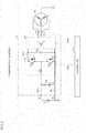
- FIG. 1 is a circuit block diagram schematically showing a configuration of a power converter according to a comparative example.
- a power converter 9 includes a positive terminal Tp and a negative terminal Tn, a positive line PL1, a negative line NL, a capacitor C1, a converter 10, a positive line PL2, a capacitor C2, an inverter 20, a U-phase terminal Tu, a V-phase terminal Tv, and a W-phase terminal Tw.
- Power converter 9 is configured to perform power conversion (DC-AC conversion) between DC power and AC power.
- a DC power supply B is, for example, a power storage device, and is a secondary battery such as a nickel-hydride battery or a lithium ion secondary battery, or a capacitor such as an electric double layer capacitor.
- DC power supply B is not limited to a secondary battery and may be a primary battery.
- DC power supply B may be a power supply (e.g., stabilized power supply) that generates DC constant voltage or a power generator (e.g., solar battery) configured to generate DC power.
- An AC motor M is an AC load that consumes AC power supplied from DC power supply B through power converter 9 to generate desired motive power. More specifically, AC motor M is a Y-connection three-phase AC motor. AC motor M may be an induction motor or a motor of any other type (e.g., synchronous motor).
- Positive terminal Tp and negative terminal Tn receive power supplied from DC power supply B.
- Positive terminal Tp is electrically connected with positive line PL1 (first power line).
- Negative terminal Tn is electrically connected with negative line NL (second power line).
- Capacitor (smoothing capacitor) C1 is electrically connected between positive line PL1 and negative line NL. Capacitor C1 smooths a DC voltage from DC power supply B and supplies the smoothed DC voltage to converter 10. Capacitor C1 has a parasitic inductance component Lp. Parasitic inductance component Lp is represented by an inductor connected in series with capacitor C1 (capacitance component) in the circuit block diagram.
- converter 10 Based on a signal PWC from a controller 100, converter 10 boosts the voltage between positive line PL1 and negative line NL and outputs the boosted voltage between positive line PL2 and negative line NL.
- Converter 10 includes a reactor Lc, switching elements Q1 and Q2, and diodes D1 and D2.
- Each of switching elements Q1 and Q2 is, for example, an insulated gate bipolar transistor (IGBT) or a power metal oxide semiconductor (MOS) transistor.
- Switching elements Q1 and Q2 are connected in series between positive line PL2 and negative line NL. Specifically, switching element Q1 has a collector connected to positive line PL2. Switching element Q1 has an emitter connected to a collector of switching element Q2. Switching element Q2 has an emitter connected to negative line NL.
- IGBT insulated gate bipolar transistor
- MOS power metal oxide semiconductor
- Reactor Lc is provided in positive line PL1. Specifically, reactor Lc has a first end electrically connected to positive line PL1. Reactor Lc has a second end electrically connected to a connection point between the emitter of switching element Q1 and the collector of switching element Q2.
- Diodes D1 and D2 are connected in anti-parallel with switching elements Q1 and Q2, respectively. In other words, diodes D1 and D2 are respectively connected in parallel with switching elements Q1 and Q2 such that the direction from the emitter side toward the collector side is a forward direction.
- converter 10 is not limited to the configuration shown in FIG. 1 as long as converter 10 includes a reactor and has an unbalanced configuration (a configuration in which the positive side and the negative side are electrically asymmetric to each other).
- Converter 10 may be, for example, a chopper circuit (e.g., non-insulated type DC/DC converter) of another type.
- Capacitor C2 is electrically connected between positive line PL2 and negative line NL. Capacitor C2 smooths a DC voltage supplied from converter 10 and supplies the smoothed DC voltage to inverter 20.
- inverter 20 Based on a signal PWI from controller 100, inverter 20 converts the DC power supplied from converter 10 to a three-phase alternating current and outputs the three-phase alternating current to AC motor M, thereby driving AC motor M.
- Inverter 20 includes a U-phase arm, a V-phase arm, and a W-phase arm (see FIG. 3 for any arm) each connected in parallel between positive line PL2 and negative line NL. Midpoints of the U-phase arm, the V-phase arm, and the W-phase arm are electrically connected to U-phase terminal Tu, V-phase terminal Tv, and W-phase terminal Tw, respectively.
- U-phase terminal Tu is configured to be connectable with a U-phase line of AC motor M.
- V-phase terminal Tv is configured to be connectable with a V-phase line of AC motor M.
- W-phase terminal Tw is configured to be connectable with a W-phase line of AC motor M.
- Controller 100 is composed of an electronic control unit including a built-in central processing unit (CPU) and a built-in memory, which are not shown. At least part of controller 100 may be configured to perform predetermined mathematical and logical operations by hardware such as an electronic circuit. Controller 100 is configured to perform various processes for controlling converter 10 and inverter 20 based on a map and a program stored in the memory. More specifically, controller 100 generates a pulse width modulation (PWM) signal for driving converter 10 by pulse width modulation and outputs the generated PWM signal to converter 10 as signal PWC. Controller 100 also generates a PWM signal for driving AC motor M and outputs the generated PWM signal to inverter 20 as signal PWI.
- PWM pulse width modulation
- Power converter 9 configured as described above generates common mode noise due to fluctuations in the midpoint potential of AC motor M by switching control of inverter 20.
- a propagation path of common mode noise and a mechanism for converting common mode noise to normal mode noise will be described below.
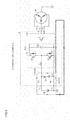
- FIG. 2 is a diagram for illustrating a noise generation mechanism and a noise conversion mechanism in power converter 9 according to the comparative example.
- common mode noise passes in a loop so as to pass through a floating capacitance to ground of AC motor M, inverter 20, converter 10, and DC power supply B in the stated order and return to AC motor M through the ground (indicated by the thick line).
- the impedance of the reactor in the step-up converter is generally greater than the impedance of the wire (positive line or negative line).
- common mode noise passes through the negative-side path (negative line NL) in which reactor Lc is not provided.
- the common mode noise that has passed through converter 10 in negative line NL is branched, at a connection point between capacitor C1 and negative line NL, into a path PATH1 (indicated by the dashed line) running to positive terminal Tp via capacitor C1 and a path PATH2 (indicated by the alternate long and short dash line) running to negative terminal Tn not via capacitor C1.
- the impedance of path PATH1 is greater than the impedance of path PATH2 by an amount by which path PATH1 includes capacitor C1 and its parasitic inductance component Lp. This causes an impedance imbalance between path PATH1 and path PATH2, so that part of the common mode noise is converted to normal mode noise.
- Path PATH1 corresponds to a "first path” according to the present invention
- path PATH2 corresponds to a "second path” according to the present invention.
- Equations (1) and (2) a current Ip flowing through positive line PL1 and a current In flowing through negative line NL are expressed by Equations (1) and (2), respectively.
- Z represents an impedance to ground of DC power supply B
- I common represents common mode noise passing through the ground
- ⁇ represents an angular frequency of common mode noise I common .
- I p Z 2 ⁇ Z + i ⁇ L p I common
- I n Z + i ⁇ L p 2 ⁇ Z + i ⁇ L p I common
- Embodiment 1 accordingly adopts a configuration in which path PATH2 is further provided with an inductor for balancing. This configuration will be described below in detail.
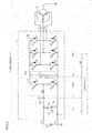
- FIG. 3 is a circuit block diagram schematically showing a configuration of a power converter according to Embodiment 1.
- power converter 1 according to Embodiment 1 differs from power converter 9 according to the comparative example (see FIG. 1 ) in that it further includes an inductor L.
- Inductor L is provided in negative line NL (second path) between capacitor C1 and negative terminal Tn. Inductor L is electrically connected to the wire (negative line NL) different from the wire (positive line PL1) connected with reactor Lc of converter 10.
- inductor L The inductance of inductor L is represented by L.
- inductor L is composed of, for example, a discrete component (e.g., coil)
- an inductance which corresponds to L may be composed of a parasitic inductance component in negative line NL.
- Inductance L may be achieved by combining the inductance of the discrete component and the parasitic inductance component of negative line NL.
- the U-phase arm of inverter 20 includes switching elements Q3 and Q4 connected in series.
- the V-phase arm includes switching elements Q5 and Q6 connected in series.
- the W-phase arm includes switching elements Q7 and Q8 connected in series. Also, switching elements Q3 to Q8 are connected in anti-parallel with diodes D3 to D8, respectively.
- a midpoint of the arm of each phase is connected to a coil of a corresponding one of the phases of AC motor M.
- Power converter 1 further includes voltage sensors 31 and 32 and a current sensor 33.
- Voltage sensor 31 detects a voltage VI across capacitor C1 as an input voltage of converter 10 and outputs the detection result to controller 100.
- Voltage sensor 32 detects a voltage V2 across capacitor C2 as an output voltage of converter 10 (an input voltage of inverter 20) and outputs the detection result to controller 100.
- Current sensor 33 detects a current I flowing through reactor Lc and outputs the detection result to controller 100. Based on a signal from each sensor, controller 100 generates a PWM signal and outputs it to converter 10 as a signal PWC, and also generates another PWM signal and outputs it to inverter 20 as signal PWI.
- FIG. 4 is a diagram for illustrating a noise propagation path in power converter 1 according to Embodiment 1.
- the noise propagation path in power converter 1 is qualitatively similar to the noise propagation path in the comparative example (see FIG. 2 ).
- conversion rate T in power converter 1 depends on a difference (Lp-L) between parasitic inductance component Lp of capacitor C1 and inductance L of inductor L in place of parasitic inductance component Lp of capacitor C1 (see Equations (4) to (6) below).
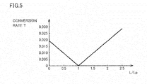
- FIG. 5 shows an example correlation between inductance L of inductor L and conversion rate T.
- the vertical axis represents conversion rate T from common mode noise I common to normal mode noise I normal .
- ( ⁇ 2 Lp 3 /Z 2 ) is negligibly smaller than 2Lp, which can be expressed as ( ⁇ 2 Lp 3 /Z 2 ) ⁇ 2Lp.
- the above condition for reducing conversion rate T can be approximated to 0 ⁇ L ⁇ 2Lp.
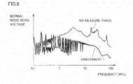
- FIG. 6 shows an example analysis result for illustrating a noise reducing effect (an effect of reducing normal mode noise) by power converter 1 according to Embodiment 1.
- the horizontal axis represents frequency on a log scale
- the vertical axis represents "normal mode noise voltage" which means a voltage applied to impedance to ground Z of DC power supply B.
- both of parasitic inductance component Lp of capacitor C1 and inductance L of inductor L were set to 30 nH.
- Impedance to ground Z of DC power supply B was set to 50 ⁇ .
- the inductance of reactor Lc was set to 60 ⁇ H.
- a line impedance stabilization network (LISN) was used to provide a constant impedance of DC power supply B as viewed from the noise source.
- inductor L having an appropriate inductance (herein, an inductance equal to parasitic inductance component Lp of capacitor C1).
- Embodiment 1 provides inductor L in negative line NL between capacitor C1 and negative terminal Tn and sets inductance L of inductor L such that the relationship 0 ⁇ L ⁇ 2Lp holds, so that a difference between the impedance of path PATH1 and the impedance of path PATH2 is smaller than in the case where inductor L is not provided.
- the impedance of path PATH1 and the impedance of path PATH2 become equal to each other by setting inductance L of inductor L to be equal to parasitic inductance component Lp of capacitor C1. This reduces (eliminates) the impedance imbalance between path PATH1 and path PATH2, thus restraining conversion from common mode noise I common to normal mode noise I normal . Consequently, switching noise can be reduced.
- reactor Lc is provided on the negative line NL side in the configuration of converter 10 differently from the configurations shown in Figs. 3 and 4 , it suffices that inductor L is provided in positive line PL1 between capacitor C1 and positive terminal Tp.
- Embodiment 1 has described the configuration in which inductor L is provided only in path PATH2, a configuration in which an inductor is provided in both of path PATH1 and path PATH2 is adoptable as described below.
- FIG. 7 is a circuit block diagram schematically showing a configuration of a power converter according to a modification of Embodiment 1.
- a power converter 1A differs from power converter 1 according to Embodiment 1 (see FIG. 3 ) in that it includes an inductor La and an inductor Lb in place of inductor L.
- Inductor La inductance: La
- inductor Lb inductance: Lb
- Each of inductors La and Lb is composed of, for example, a discrete component (e.g., coil). At least one of inductors La and Lb may be formed by adjusting the parasitic inductance component of the wire (positive line PL1 or negative line NL). Alternatively, inductors La and Lb each may be composed of a normal mode choke coil in which the positive side and the negative side have an asymmetrical shape. Since the noise propagation path in power converter 1A is similar to the noise propagation path shown in FIG. 4 , detailed description by illustration will not be repeated.
- Equation (9) reveals that conversion rate T depends on (Lp+La-Lb).
- I p Z + i ⁇ ⁇ L b 2 ⁇ Z + i ⁇ ⁇ L p + L a + L b
- I common I n Z + i ⁇ L p + L a 2 ⁇ Z + i ⁇ L p + L a + L b
- the inductances of inductors La and Lb are set such that the relationship 0 ⁇ Lb-La ⁇ 2Lp holds also in the configuration in which inductor La is provided in positive line PL1 between capacitor C1 and positive terminal Tp and inductor Lb is provided in negative line NL between capacitor C1 and negative terminal Tn, as described above.
- the inductance (Lb) of path PATH2 and the inductance (La) of path PATH1 are set such that a difference therebetween (Lb-La) is less than twice parasitic inductance component Lp of capacitor C1.
- the difference between the impedance of path PATH1 and the impedance of path PATH2 is smaller than in the case where inductors La and Lb are not provided. This can restrain conversion from common mode noise I common to normal mode noise I normal , thus reducing switching noise.
- another inductor may be provided in place of inductor L in the configuration of Embodiment 1 shown in FIG. 3 . That is to say, though not shown, an inductor having an inductance equal to that of reactor Lc provided in positive line PL1 can be provided in negative line NL between capacitor C1 and switching element Q2.
- an inductor larger in size than inductor L in Embodiment 1 is necessary for obtaining an imbalance reducing effect as in the configuration of Embodiment 1.
- an inductor larger in size than inductors La and Lb (see FIG. 5 ) in the modification is necessary. That is to say, Embodiment 1 and the modification thereof can reduce switching noise by the installation of an inductor of smaller size.
- Embodiment 1 and the modification thereof have described the configuration in which an inductor is provided in either or both of path PATH1 and path PATH2.
- a circuit component provided in the path is not limited to an inductor as long as the impedance difference between path PATH1 and path PATH2 is smaller and the impedance imbalance is eliminated (reduced).
- Embodiment 2 will describe a configuration in which a resistor is provided in path PATH2.
- FIG. 8 is a circuit block diagram schematically showing a configuration of a power converter according to Embodiment 2.
- capacitor C1 has a parasitic resistance component Rp.
- Parasitic resistance component Rp is expressed as a resistor connected in series with capacitor C1 (capacitance component) in the circuit block diagram.
- Power converter 2 differs from power converter 1 according to Embodiment 1 (see FIG. 3 ) in that it includes a resistor R in place of inductor L. Resistor R is electrically connected to negative line NL between capacitor C1 and negative terminal Tn. Although resistor R is composed of, for example, a discrete component (e.g., chip resistor), it may be composed of a wiring resistor (parasitic resistor) of negative line NL. Alternatively, resistor R may be achieved by, for example, combining a chip resistor and a wiring resistor of negative line NL.
- resistor R may be achieved by, for example, combining a chip resistor and a wiring resistor of negative line NL.
- power converter 2 Other components of power converter 2 are similar to the corresponding components of power converter 1 according to Embodiment 1 (see FIG. 3 ). Also, the noise propagation path in power converter 2 is similar to the noise propagation path shown in FIG. 4 . Detailed description will thus not be repeated.
- resistor R is electrically connected to negative line NL between capacitor C1 and negative terminal Tn, as described above.
- resistor R By setting resistor R such that the difference between the resistance of path PATH2 and the resistance of path PATH1 is less than twice parasitic resistance component Rp of capacitor C1, that is, such that the relationship 0 ⁇ Rp-R ⁇ 2Rp holds, the difference between the impedance of path PATH1 and the impedance of path PATH2 becomes smaller than in the case where resistor R is not provided. This can restrain conversion from common mode noise I common to normal mode noise I normal , thus reducing switching noise.
- Embodiment 2 can adopt the configuration in which a resistor is provided in both of path PATH1 and path PATH2 as in the modification of Embodiment 1.
Landscapes
- Engineering & Computer Science (AREA)
- Power Engineering (AREA)
- Inverter Devices (AREA)
- Dc-Dc Converters (AREA)
Abstract
Description
- The present invention relates to a power converter that performs power conversion between a DC power supply and an AC load, and more particularly, to a power converter that includes a converter including a reactor and performs power conversion between the DC power supply and the AC load.
- A power converter is known that performs power conversion between a DC power supply and an AC load by switching control. In switching control of high frequency (e.g., a frequency of 20 kHz or more), high-frequency noise (switching noise) may occur resulting from switching of a switching element of an inverter in the power converter. A mechanism for generating such switching noise is described as follows. A neutral potential of an AC load (e.g., AC motor) varies due to switching of the inverter, causing common mode noise.
- If the circuitry of the power converter is unbalanced between the positive side and the negative side, mode conversion may occur between common mode noise and normal mode noise. Specifically, common mode noise may be converted to normal mode noise, or normal mode noise may be converted to common mode noise. A technique is thus proposed for preventing mode conversion to reduce switching noise.
- For example, the power converter disclosed in Japanese Patent Laying-Open No.
2009-296756 PTL 1, the center tap is connected to a connection point between the high-potential-side Y-capacitor and the low-potential-side Y-capacitor. This causes the impedance of the first loop circuit and the impedance of the second loop circuit to be equal to each other. This cancels the imbalance between the power converters, so that mode conversion can be prevented (e.g., see paragraph [0038] of PTL 1). -
- PTL 1: Japanese Patent Laying-Open No.
2009-296756 - PTL 2: Japanese Patent Laying-Open No.
2012-29404 - PTL 3: International Publication No.
2013/99540 - The power converter disclosed in
PTL 1 steps down the voltage (e.g., several hundreds of volts) of a high-voltage battery and outputs a resultant voltage to a low-voltage battery (e.g., 12-V battery), and has a configuration including an insulating converter including a transformer (e.g., see paragraphs [0028] to [0032] andFIG. 1 of PTL 1). - Meanwhile, a power converter having a configuration including a converter including a reactor has been widely used.
PTL 1 does not particularly describe such a configuration including a converter, and also does not describe a study on a reduction in the switching noise in such a configuration. It is desirable that switching noise be preferably reduced also in the power converter including a converter with a reactor. - The present invention has been made to solve the above problem, and has an object to preferably reduce switching noise in a power converter that includes a converter including a reactor and performs power conversion between a DC power supply and an AC load.
-
- (1) A power converter according to an aspect of the present invention includes a positive terminal and a negative terminal, first and second power lines, a smoothing capacitor, a converter, and an inverter. The positive terminal and the negative terminal receive power supplied from a DC power supply. The first power line is electrically connected with a first terminal among the positive terminal and the negative terminal. The second power line is electrically connected with a second terminal among the positive terminal and the negative terminal. The smoothing capacitor has a parasitic inductance component and is electrically connected between the first power line and the second power line. The converter includes a reactor provided in the first power line and performs voltage conversion of a DC voltage smoothed by the smoothing capacitor. The inverter performs DC-AC conversion between the converter and an AC load by switching control. A first path of the first power line has an inductance smaller than an inductance of a second path of the second power line. The first path connects the first terminal and the smoothing capacitor. The second path connects the second terminal and the smoothing capacitor. A difference between the inductance of the second path and the inductance of the first path is less than twice the parasitic inductance component of the smoothing capacitor.
- (2) Preferably, the power converter further includes an inductor provided in the second path. The inductor has an inductance less than twice the parasitic inductance component of the smoothing capacitor.
- (3) Preferably, the inductance of the second path is a parasitic inductance component of the second path. The parasitic inductance component of the second path is less than twice the parasitic inductance component of the smoothing capacitor.
- (4) Preferably, the power converter further includes a first inductor provided in the first path and a second inductor provided in the second path. A difference between an inductance of the second inductor and an inductance of the first inductor is less than twice the parasitic inductance component of the smoothing capacitor.
- (5) A power converter according to another aspect of the present invention includes a positive terminal and a negative terminal, first and second power lines, a smoothing capacitor, a converter, and an inverter. The positive terminal and the negative terminal receive power supplied from a DC power supply. The first power line is electrically connected with a first terminal among the positive terminal and the negative terminal. The second power line is electrically connected with a second terminal among the positive terminal and the negative terminal. The smoothing capacitor has a parasitic resistance component and is electrically connected between the first power line and the second power line. The converter includes a reactor provided in the first power line and performs voltage conversion of a DC voltage smoothed by the smoothing capacitor. The inverter performs DC-AC conversion between the converter and an AC load by switching control. A first path of the first power line has a resistance smaller than a resistance of a second path of the second power line. The first path connects the first terminal and the smoothing capacitor. The second path connects the second terminal and the smoothing capacitor. A difference between the resistance of the second path and the resistance of the first path is less than twice the parasitic resistance component of the smoothing capacitor.
- The present invention can preferably reduce switching noise in a power converter that includes a converter including a reactor and performs power conversion between a DC power supply and an AC load.
-
- FIG. 1
- is a circuit block diagram schematically showing a configuration of a power converter according to a comparative example.
- FIG. 2
- is a diagram for illustrating a noise generation mechanism and a noise conversion mechanism in the power converter in the comparative example.
- FIG. 3
- is a circuit block diagram schematically showing a configuration of a power converter according to
Embodiment 1. - FIG. 4
- is a diagram for illustrating a noise propagation path in the power converter according to
Embodiment 1. - FIG. 5
- shows an example correlation between the inductance of an inductor L and a conversion rate.
- FIG. 6
- shows an example analysis result for illustrating a noise reducing effect by the power converter according to
Embodiment 1. - FIG. 7
- is a circuit block diagram schematically showing a configuration of a power converter according to a modification of
Embodiment 1. - FIG. 8
- is a circuit block diagram schematically showing a configuration of a power converter according to
Embodiment 2. - Embodiments for implementing the present invention will be described below in detail with reference to the drawings. The same or corresponding parts are designated by the same references, and description thereof will not be repeated.
- A configuration of a power converter according to a comparative example will now be described for easy understanding of the features of a power converter according to
Embodiment 1. -
FIG. 1 is a circuit block diagram schematically showing a configuration of a power converter according to a comparative example. Referring toFIG. 1 , apower converter 9 includes a positive terminal Tp and a negative terminal Tn, a positive line PL1, a negative line NL, a capacitor C1, aconverter 10, a positive line PL2, a capacitor C2, aninverter 20, a U-phase terminal Tu, a V-phase terminal Tv, and a W-phase terminalTw. Power converter 9 is configured to perform power conversion (DC-AC conversion) between DC power and AC power. - A DC power supply B is, for example, a power storage device, and is a secondary battery such as a nickel-hydride battery or a lithium ion secondary battery, or a capacitor such as an electric double layer capacitor. DC power supply B is not limited to a secondary battery and may be a primary battery. Alternatively, DC power supply B may be a power supply (e.g., stabilized power supply) that generates DC constant voltage or a power generator (e.g., solar battery) configured to generate DC power.
- An AC motor M is an AC load that consumes AC power supplied from DC power supply B through
power converter 9 to generate desired motive power. More specifically, AC motor M is a Y-connection three-phase AC motor. AC motor M may be an induction motor or a motor of any other type (e.g., synchronous motor). - Positive terminal Tp and negative terminal Tn receive power supplied from DC power supply B. Positive terminal Tp is electrically connected with positive line PL1 (first power line). Negative terminal Tn is electrically connected with negative line NL (second power line).
- Capacitor (smoothing capacitor) C1 is electrically connected between positive line PL1 and negative line NL. Capacitor C1 smooths a DC voltage from DC power supply B and supplies the smoothed DC voltage to
converter 10. Capacitor C1 has a parasitic inductance component Lp. Parasitic inductance component Lp is represented by an inductor connected in series with capacitor C1 (capacitance component) in the circuit block diagram. - Based on a signal PWC from a
controller 100,converter 10 boosts the voltage between positive line PL1 and negative line NL and outputs the boosted voltage between positive line PL2 and negative line NL.Converter 10 includes a reactor Lc, switching elements Q1 and Q2, and diodes D1 and D2. - Each of switching elements Q1 and Q2 is, for example, an insulated gate bipolar transistor (IGBT) or a power metal oxide semiconductor (MOS) transistor. Switching elements Q1 and Q2 are connected in series between positive line PL2 and negative line NL. Specifically, switching element Q1 has a collector connected to positive line PL2. Switching element Q1 has an emitter connected to a collector of switching element Q2. Switching element Q2 has an emitter connected to negative line NL.
- Reactor Lc is provided in positive line PL1. Specifically, reactor Lc has a first end electrically connected to positive line PL1. Reactor Lc has a second end electrically connected to a connection point between the emitter of switching element Q1 and the collector of switching element Q2.
- Diodes D1 and D2 are connected in anti-parallel with switching elements Q1 and Q2, respectively. In other words, diodes D1 and D2 are respectively connected in parallel with switching elements Q1 and Q2 such that the direction from the emitter side toward the collector side is a forward direction.
- The configuration of
converter 10 is not limited to the configuration shown inFIG. 1 as long asconverter 10 includes a reactor and has an unbalanced configuration (a configuration in which the positive side and the negative side are electrically asymmetric to each other).Converter 10 may be, for example, a chopper circuit (e.g., non-insulated type DC/DC converter) of another type. - Capacitor C2 is electrically connected between positive line PL2 and negative line NL. Capacitor C2 smooths a DC voltage supplied from
converter 10 and supplies the smoothed DC voltage toinverter 20. - Based on a signal PWI from
controller 100,inverter 20 converts the DC power supplied fromconverter 10 to a three-phase alternating current and outputs the three-phase alternating current to AC motor M, thereby driving ACmotor M. Inverter 20 includes a U-phase arm, a V-phase arm, and a W-phase arm (seeFIG. 3 for any arm) each connected in parallel between positive line PL2 and negative line NL. Midpoints of the U-phase arm, the V-phase arm, and the W-phase arm are electrically connected to U-phase terminal Tu, V-phase terminal Tv, and W-phase terminal Tw, respectively. - U-phase terminal Tu is configured to be connectable with a U-phase line of AC motor M. V-phase terminal Tv is configured to be connectable with a V-phase line of AC motor M. W-phase terminal Tw is configured to be connectable with a W-phase line of AC motor M.
-
Controller 100 is composed of an electronic control unit including a built-in central processing unit (CPU) and a built-in memory, which are not shown. At least part ofcontroller 100 may be configured to perform predetermined mathematical and logical operations by hardware such as an electronic circuit.Controller 100 is configured to perform various processes for controllingconverter 10 andinverter 20 based on a map and a program stored in the memory. More specifically,controller 100 generates a pulse width modulation (PWM) signal for drivingconverter 10 by pulse width modulation and outputs the generated PWM signal toconverter 10 as signal PWC.Controller 100 also generates a PWM signal for driving AC motor M and outputs the generated PWM signal toinverter 20 as signal PWI. -
Power converter 9 configured as described above generates common mode noise due to fluctuations in the midpoint potential of AC motor M by switching control ofinverter 20. A propagation path of common mode noise and a mechanism for converting common mode noise to normal mode noise will be described below. -
FIG. 2 is a diagram for illustrating a noise generation mechanism and a noise conversion mechanism inpower converter 9 according to the comparative example. Schematically, referring toFIG. 2 , common mode noise passes in a loop so as to pass through a floating capacitance to ground of AC motor M,inverter 20,converter 10, and DC power supply B in the stated order and return to AC motor M through the ground (indicated by the thick line). - More specifically, although the magnitude of the common mode noise generated by switching control is equal between a positive-side path (path through positive lines PL1 and PL2) and a negative-side path (path through negative line NL) of
power converter 9, the impedance of the reactor in the step-up converter is generally greater than the impedance of the wire (positive line or negative line). In the configuration in which reactor Lc is provided in the positive-side path (positive line PL1) as inpower converter 9, thus, common mode noise passes through the negative-side path (negative line NL) in which reactor Lc is not provided. - The common mode noise that has passed through
converter 10 in negative line NL is branched, at a connection point between capacitor C1 and negative line NL, into a path PATH1 (indicated by the dashed line) running to positive terminal Tp via capacitor C1 and a path PATH2 (indicated by the alternate long and short dash line) running to negative terminal Tn not via capacitor C1. The impedance of path PATH1 is greater than the impedance of path PATH2 by an amount by which path PATH1 includes capacitor C1 and its parasitic inductance component Lp. This causes an impedance imbalance between path PATH1 and path PATH2, so that part of the common mode noise is converted to normal mode noise. Path PATH1 corresponds to a "first path" according to the present invention, and path PATH2 corresponds to a "second path" according to the present invention. - Herein, a current Ip flowing through positive line PL1 and a current In flowing through negative line NL are expressed by Equations (1) and (2), respectively. In Equations (1) and (2) (and equations described below), Z represents an impedance to ground of DC power supply B, Icommon represents common mode noise passing through the ground, and ω represents an angular frequency of common mode noise Icommon.
Math 1


- Normal mode noise Inormal is calculated as a difference (In-Ip) between current In and current Ip, and is expressed as shown in Equation (3). Equation (3) reveals that a conversion rate T (T=Inormal/Icommon) from common mode noise Icommon to normal mode noise Inormal depends on parasitic inductance component Lp of capacitor C1. Conversion rate T from common mode noise Icommon to normal mode noise Inormal may be abbreviated as "conversion rate T" below.
- In the comparative example, an impedance imbalance occurs between path PATH1 and path PATH2 due to the presence of parasitic inductance component Lp of capacitor C1 as described above. Consequently, conversion from common mode noise Icommon to normal mode noise Inormal is liable to occur, which may cause switching noise.
Embodiment 1 accordingly adopts a configuration in which path PATH2 is further provided with an inductor for balancing. This configuration will be described below in detail. -
FIG. 3 is a circuit block diagram schematically showing a configuration of a power converter according toEmbodiment 1. Referring toFIG. 3 ,power converter 1 according toEmbodiment 1 differs frompower converter 9 according to the comparative example (seeFIG. 1 ) in that it further includes an inductor L. - Inductor L is provided in negative line NL (second path) between capacitor C1 and negative terminal Tn. Inductor L is electrically connected to the wire (negative line NL) different from the wire (positive line PL1) connected with reactor Lc of
converter 10. - The inductance of inductor L is represented by L. Although inductor L is composed of, for example, a discrete component (e.g., coil), an inductance which corresponds to L may be composed of a parasitic inductance component in negative line NL. Inductance L may be achieved by combining the inductance of the discrete component and the parasitic inductance component of negative line NL.
- A specific configuration of
power converter 1 will be described further. The U-phase arm ofinverter 20 includes switching elements Q3 and Q4 connected in series. The V-phase arm includes switching elements Q5 and Q6 connected in series. The W-phase arm includes switching elements Q7 and Q8 connected in series. Also, switching elements Q3 to Q8 are connected in anti-parallel with diodes D3 to D8, respectively. A midpoint of the arm of each phase is connected to a coil of a corresponding one of the phases of AC motor M. -
Power converter 1 further includesvoltage sensors current sensor 33.Voltage sensor 31 detects a voltage VI across capacitor C1 as an input voltage ofconverter 10 and outputs the detection result tocontroller 100.Voltage sensor 32 detects a voltage V2 across capacitor C2 as an output voltage of converter 10 (an input voltage of inverter 20) and outputs the detection result tocontroller 100.Current sensor 33 detects a current I flowing through reactor Lc and outputs the detection result tocontroller 100. Based on a signal from each sensor,controller 100 generates a PWM signal and outputs it toconverter 10 as a signal PWC, and also generates another PWM signal and outputs it to inverter 20 as signal PWI. - Since the other components of
power converter 1 are similar to the corresponding components ofpower converter 9 according to the comparative example, detailed description will not be repeated. Specific configurations ofconverter 10 andinverter 20 are not limited to the example shown inFIG. 3 .Voltage sensors current sensor 33 are not essential components in the present invention. -
FIG. 4 is a diagram for illustrating a noise propagation path inpower converter 1 according toEmbodiment 1. Referring toFIG. 4 , the noise propagation path inpower converter 1 is qualitatively similar to the noise propagation path in the comparative example (seeFIG. 2 ). - In
power converter 1, however, the ratio between the impedance of path PATH1 and the impedance of path PATH2 changes due to the provision of inductor L. Consequently, conversion rate T inpower converter 1 depends on a difference (Lp-L) between parasitic inductance component Lp of capacitor C1 and inductance L of inductor L in place of parasitic inductance component Lp of capacitor C1 (see Equations (4) to (6) below).
Math 2


-
FIG. 5 shows an example correlation between inductance L of inductor L and conversion rate T. InFIG. 5 , the horizontal axis represents the ratio (=L/Lp) of inductance L of inductor L to parasitic inductance component Lp of capacitor C1, and the vertical axis represents conversion rate T from common mode noise Icommon to normal mode noise Inormal. - In comparison between Equation (3) and Equation (6), when the coefficient (absolute value) of common mode noise Icommon on the right side of Equation (6) is smaller than the coefficient (absolute value) of common mode noise Icommon on the right side of Equation (3), that is, when the
relationship 0<L<2Lp+(ω2Lp3/Z2) holds after the change and arrangement of these equations, conversion rate T becomes lower by providing inductor L than in the case where inductor L is not provided. - For example, when inductance L of inductor L is equal to parasitic inductance component Lp of capacitor C1 (when L/Lp=1), conversion rate T is zero as shown in
FIG. 5 . That is to say, normal mode noise Inormal is smallest when inductance L of inductor L is equal to parasitic inductance component Lp of capacitor C1. - In many cases, (ω2Lp3/Z2) is negligibly smaller than 2Lp, which can be expressed as (ω2Lp3/Z2)<<2Lp. In such cases, the above condition for reducing conversion rate T can be approximated to 0<L<2Lp.
-
FIG. 6 shows an example analysis result for illustrating a noise reducing effect (an effect of reducing normal mode noise) bypower converter 1 according toEmbodiment 1. InFIG. 6 , the horizontal axis represents frequency on a log scale, and the vertical axis represents "normal mode noise voltage" which means a voltage applied to impedance to ground Z of DC power supply B. - In the analysis example shown in
FIG. 6 , both of parasitic inductance component Lp of capacitor C1 and inductance L of inductor L were set to 30 nH. Impedance to ground Z of DC power supply B was set to 50 Ω. The inductance of reactor Lc was set to 60 µH. In this analysis, a line impedance stabilization network (LISN) was used to provide a constant impedance of DC power supply B as viewed from the noise source. - As shown in
FIG. 6 , it can be found that the normal mode noise can be reduced over a wide frequency range by providing inductor L having an appropriate inductance (herein, an inductance equal to parasitic inductance component Lp of capacitor C1). - As described above,
Embodiment 1 provides inductor L in negative line NL between capacitor C1 and negative terminal Tn and sets inductance L of inductor L such that therelationship 0<L<2Lp holds, so that a difference between the impedance of path PATH1 and the impedance of path PATH2 is smaller than in the case where inductor L is not provided. In particular, the impedance of path PATH1 and the impedance of path PATH2 become equal to each other by setting inductance L of inductor L to be equal to parasitic inductance component Lp of capacitor C1. This reduces (eliminates) the impedance imbalance between path PATH1 and path PATH2, thus restraining conversion from common mode noise Icommon to normal mode noise Inormal. Consequently, switching noise can be reduced. - Although not shown, when reactor Lc is provided on the negative line NL side in the configuration of
converter 10 differently from the configurations shown inFigs. 3 and4 , it suffices that inductor L is provided in positive line PL1 between capacitor C1 and positive terminal Tp. - Although
Embodiment 1 has described the configuration in which inductor L is provided only in path PATH2, a configuration in which an inductor is provided in both of path PATH1 and path PATH2 is adoptable as described below. -
FIG. 7 is a circuit block diagram schematically showing a configuration of a power converter according to a modification ofEmbodiment 1. Referring toFIG. 7 , apower converter 1A differs frompower converter 1 according to Embodiment 1 (seeFIG. 3 ) in that it includes an inductor La and an inductor Lb in place of inductor L. - Inductor La (inductance: La) is provided in positive line PL1 between capacitor C1 and positive terminal Tp, whereas inductor Lb (inductance: Lb) is provided in negative line NL between capacitor C1 and negative terminal Tn.
- Each of inductors La and Lb is composed of, for example, a discrete component (e.g., coil). At least one of inductors La and Lb may be formed by adjusting the parasitic inductance component of the wire (positive line PL1 or negative line NL). Alternatively, inductors La and Lb each may be composed of a normal mode choke coil in which the positive side and the negative side have an asymmetrical shape. Since the noise propagation path in
power converter 1A is similar to the noise propagation path shown inFIG. 4 , detailed description by illustration will not be repeated. - Current Ip flowing through positive line PL1, and current In and normal mode noise Inormal passing through negative line NL are expressed by Equations (7) to (9) below, respectively. Equation (9) reveals that conversion rate T depends on (Lp+La-Lb).
Math 3


- In comparison between Equation (3) and Equation (9) above, when the coefficient (absolute value) of common mode noise Icommon on the right side of Equation (9) is smaller than the coefficient (absolute value) of common mode noise Icommon on the right side of Equation (3), that is, when the
relationship 0<Lb-La<2Lp+(ω2Lp3/Z2) holds after the change and arrangement of these equations, conversion rate T becomes lower by providing inductors La and Lb than in the case where inductors La and Lb are not provided. - When (ω2Lp3/Z2) is negligibly smaller than 2Lp and can be expressed as (ω2Lp3/Z2) <<2Lp, the above condition for reducing conversion rate T can be approximated to 0<Lb-La<2Lp.
- Since conversion rate T is zero when the relationship Lb-La=Lp holds as in
Embodiment 1, normal mode noise Inormal is smallest. - According to the modification of
Embodiment 1, the inductances of inductors La and Lb are set such that therelationship 0<Lb-La<2Lp holds also in the configuration in which inductor La is provided in positive line PL1 between capacitor C1 and positive terminal Tp and inductor Lb is provided in negative line NL between capacitor C1 and negative terminal Tn, as described above. In this manner, the inductance (Lb) of path PATH2 and the inductance (La) of path PATH1 are set such that a difference therebetween (Lb-La) is less than twice parasitic inductance component Lp of capacitor C1. Consequently, the difference between the impedance of path PATH1 and the impedance of path PATH2 is smaller than in the case where inductors La and Lb are not provided. This can restrain conversion from common mode noise Icommon to normal mode noise Inormal, thus reducing switching noise. - From the viewpoint of reducing the impedance imbalance between path PATH1 and path PATH2, another inductor may be provided in place of inductor L in the configuration of
Embodiment 1 shown inFIG. 3 . That is to say, though not shown, an inductor having an inductance equal to that of reactor Lc provided in positive line PL1 can be provided in negative line NL between capacitor C1 and switching element Q2. When such a configuration is adopted, however, an inductor larger in size than inductor L inEmbodiment 1 is necessary for obtaining an imbalance reducing effect as in the configuration ofEmbodiment 1. Also, an inductor larger in size than inductors La and Lb (seeFIG. 5 ) in the modification is necessary. That is to say,Embodiment 1 and the modification thereof can reduce switching noise by the installation of an inductor of smaller size. -
Embodiment 1 and the modification thereof have described the configuration in which an inductor is provided in either or both of path PATH1 and path PATH2. However, a circuit component provided in the path (at least one of path PATH1 and path PATH2) is not limited to an inductor as long as the impedance difference between path PATH1 and path PATH2 is smaller and the impedance imbalance is eliminated (reduced).Embodiment 2 will describe a configuration in which a resistor is provided in path PATH2. -
FIG. 8 is a circuit block diagram schematically showing a configuration of a power converter according toEmbodiment 2. Referring toFIG. 8 , capacitor C1 has a parasitic resistance component Rp. Parasitic resistance component Rp is expressed as a resistor connected in series with capacitor C1 (capacitance component) in the circuit block diagram. -
Power converter 2 differs frompower converter 1 according to Embodiment 1 (seeFIG. 3 ) in that it includes a resistor R in place of inductor L. Resistor R is electrically connected to negative line NL between capacitor C1 and negative terminal Tn. Although resistor R is composed of, for example, a discrete component (e.g., chip resistor), it may be composed of a wiring resistor (parasitic resistor) of negative line NL. Alternatively, resistor R may be achieved by, for example, combining a chip resistor and a wiring resistor of negative line NL. - Other components of
power converter 2 are similar to the corresponding components ofpower converter 1 according to Embodiment 1 (seeFIG. 3 ). Also, the noise propagation path inpower converter 2 is similar to the noise propagation path shown inFIG. 4 . Detailed description will thus not be repeated. - In
Embodiment 2, current Ip flowing through positive line PL1, and current In and normal mode noise Inormal passing through negative line NL are expressed by Equations (10) to (12) below, respectively. Equation (12) reveals that conversion rate T depends on (Rp-R).
Math 4


- As in
Embodiment 1, in comparison between Equation (3) and Equation (12), when therelationship 0<Rp-R<2Rp+(Rp3/Z2) holds after the change and arrangement of these equations, conversion rate T becomes lower by providing resistor R than in the case where resistor R is not provided. When (Rp3/Z2) is negligibly smaller than 2Lp (when expressed as (Rp3/Z2) <<2Lp), the condition for reducing conversion rate T can be approximated to 0<Rp-R<2Rp. Also, since conversion rate T is zero when R=Rp, normal mode noise Inormal is smallest. - In
Embodiment 2, resistor R is electrically connected to negative line NL between capacitor C1 and negative terminal Tn, as described above. By setting resistor R such that the difference between the resistance of path PATH2 and the resistance of path PATH1 is less than twice parasitic resistance component Rp of capacitor C1, that is, such that therelationship 0<Rp-R<2Rp holds, the difference between the impedance of path PATH1 and the impedance of path PATH2 becomes smaller than in the case where resistor R is not provided. This can restrain conversion from common mode noise Icommon to normal mode noise Inormal, thus reducing switching noise. - Although detailed description will not be repeated,
Embodiment 2 can adopt the configuration in which a resistor is provided in both of path PATH1 and path PATH2 as in the modification ofEmbodiment 1. - It is to be understood that the embodiments disclosed herein are presented for the purpose of illustration and non-restrictive in every respect. It is therefore intended that the scope of the present invention is defined by claims, not only by the embodiments described above, and encompasses all modifications and variations equivalent in meaning and scope to the claims.
-
- 1, 1A, 2, 9
- power converter
- 10
- converter
- 20
- inverter
- 31, 32
- voltage sensor
- 33
- current sensor
- 100
- controller
- B DC
- power supply
- C1, C2
- capacitor
- D1-D8
- diode
- I, In, Ip
- current
- L, La, Lb
- inductor
- Lc
- reactor
- Lp
- parasitic inductance component
- M
- AC motor
- PL1, PL2
- positive line
- NL
- negative line
- Q1-Q8
- switching element
- R
- resistor
- Rp
- parasitic resistance component
- Tn
- negative terminal
- Tp
- positive terminal
- Tu
- U-phase terminal
- Tv
- V-phase terminal
- Tw
- W-phase terminal.
Claims (5)
- A power converter comprising:a positive terminal and a negative terminal that receive power supplied from a DC power supply;a first power line electrically connected with a first terminal among the positive terminal and the negative terminal;a second power line electrically connected with a second terminal among the positive terminal and the negative terminal;a smoothing capacitor having a parasitic inductance component and electrically connected between the first power line and the second power line;a converter including a reactor provided in the first power line, the converter performing voltage conversion of a DC voltage smoothed by the smoothing capacitor; andan inverter that performs DC-AC conversion between the converter and an AC load by switching control, whereina first path of the first power line has an inductance smaller than an inductance of a second path of the second power line,the first path connects the first terminal and the smoothing capacitor, the second path connects the second terminal and the smoothing capacitor, anda difference between the inductance of the second path and the inductance of the first path is less than twice the parasitic inductance component of the smoothing capacitor.
- The power converter according to claim 1, further comprising an inductor provided in the second path,
wherein the inductor has an inductance less than twice the parasitic inductance component of the smoothing capacitor. - The power converter according to claim 1, wherein
the inductance of the second path is a parasitic inductance component of the second path, and
the parasitic inductance component of the second path is less than twice the parasitic inductance component of the smoothing capacitor. - The power converter according to claim 1, further comprising:a first inductor provided in the first path; anda second inductor provided in the second path,wherein a difference between an inductance of the second inductor and an inductance of the first inductor is less than twice the parasitic inductance component of the smoothing capacitor.
- A power converter comprising:a positive terminal and a negative terminal that receive power supplied from a DC power supply;a first power line electrically connected with a first terminal among the positive terminal and the negative terminal;a second power line electrically connected with a second terminal among the positive terminal and the negative terminal;a smoothing capacitor having a parasitic resistance component and electrically connected between the first power line and the second power line;a converter including a reactor electrically connected to the first power line, the converter performing voltage conversion; andan inverter that performs DC-AC conversion between the converter and an AC load by switching control, whereina first path of the first power line has a resistance smaller than a resistance of a second path of the second power line,the first path connects the first terminal and the smoothing capacitor, the second path connects the second terminal and the smoothing capacitor, anda difference between the resistance of the second path and the resistance of the first path is less than twice the parasitic resistance component of the smoothing capacitor.
Applications Claiming Priority (2)
| Application Number | Priority Date | Filing Date | Title |
|---|---|---|---|
| JP2017113073 | 2017-06-08 | ||
| PCT/JP2018/005519 WO2018225301A1 (en) | 2017-06-08 | 2018-02-16 | Power conversion device |
Publications (2)
| Publication Number | Publication Date |
|---|---|
| EP3637604A1 true EP3637604A1 (en) | 2020-04-15 |
| EP3637604A4 EP3637604A4 (en) | 2020-05-20 |
Family
ID=64566697
Family Applications (1)
| Application Number | Title | Priority Date | Filing Date |
|---|---|---|---|
| EP18813865.5A Withdrawn EP3637604A4 (en) | 2017-06-08 | 2018-02-16 | ENERGY CONVERSION DEVICE |
Country Status (5)
| Country | Link |
|---|---|
| US (1) | US10804814B2 (en) |
| EP (1) | EP3637604A4 (en) |
| JP (1) | JP6385626B1 (en) |
| CN (1) | CN110692186B (en) |
| WO (1) | WO2018225301A1 (en) |
Families Citing this family (3)
| Publication number | Priority date | Publication date | Assignee | Title |
|---|---|---|---|---|
| JP7135949B2 (en) * | 2019-03-14 | 2022-09-13 | 株式会社デンソー | power converter |
| JP7472853B2 (en) * | 2021-05-27 | 2024-04-23 | 株式会社デンソー | Power Conversion Equipment |
| CN113746331A (en) * | 2021-08-30 | 2021-12-03 | 西安交通大学 | Resonant switched capacitor converter using parasitic inductance |
Family Cites Families (12)
| Publication number | Priority date | Publication date | Assignee | Title |
|---|---|---|---|---|
| JP4565451B2 (en) * | 2006-01-27 | 2010-10-20 | ダイヤモンド電機株式会社 | Digital converter and control method thereof |
| US7589605B2 (en) * | 2006-02-15 | 2009-09-15 | Massachusetts Institute Of Technology | Method and apparatus to provide compensation for parasitic inductance of multiple capacitors |
| JP2009296756A (en) | 2008-06-04 | 2009-12-17 | Denso Corp | Power conversion device |
| TWI454028B (en) * | 2010-01-13 | 2014-09-21 | Toshiba Kk | System interconnection converter |
| JP5721355B2 (en) | 2010-07-21 | 2015-05-20 | キヤノン株式会社 | Power circuit |
| EP2525491B1 (en) * | 2011-05-16 | 2021-03-10 | Vincotech GmbH | Switching loss reduction in converter modules |
| WO2013099540A1 (en) | 2011-12-27 | 2013-07-04 | 株式会社村田製作所 | Laminated common-mode choke coil |
| JP6041862B2 (en) * | 2012-03-05 | 2016-12-14 | 富士電機株式会社 | Power converter |
| JP2014042410A (en) * | 2012-08-23 | 2014-03-06 | Toyota Motor Corp | Polyphase converter system |
| JP5869461B2 (en) * | 2012-10-17 | 2016-02-24 | 山洋電気株式会社 | Grid-connected power supply system |
| US9893603B2 (en) * | 2014-06-06 | 2018-02-13 | Hitachi Automotive Systems, Ltd. | Power converter |
| EP3512085A1 (en) * | 2018-01-12 | 2019-07-17 | Fraunhofer-Gesellschaft zur Förderung der angewandten Forschung e.V. | Dc/dc converters with parasitic resonance circuits and ultra-steep switching slopes |
-
2018
- 2018-02-16 WO PCT/JP2018/005519 patent/WO2018225301A1/en not_active Ceased
- 2018-02-16 EP EP18813865.5A patent/EP3637604A4/en not_active Withdrawn
- 2018-02-16 CN CN201880035628.1A patent/CN110692186B/en active Active
- 2018-02-16 JP JP2018526820A patent/JP6385626B1/en active Active
- 2018-02-16 US US16/609,251 patent/US10804814B2/en active Active
Also Published As
| Publication number | Publication date |
|---|---|
| JPWO2018225301A1 (en) | 2019-06-27 |
| WO2018225301A1 (en) | 2018-12-13 |
| US10804814B2 (en) | 2020-10-13 |
| EP3637604A4 (en) | 2020-05-20 |
| CN110692186A (en) | 2020-01-14 |
| CN110692186B (en) | 2022-01-11 |
| JP6385626B1 (en) | 2018-09-05 |
| US20200099314A1 (en) | 2020-03-26 |
Similar Documents
| Publication | Publication Date | Title |
|---|---|---|
| US8625307B2 (en) | DC to AC power converting apparatus | |
| US20170338764A1 (en) | Control apparatus for power conversion apparatus | |
| US9487098B2 (en) | Power conversion apparatus | |
| JPWO2015056571A1 (en) | Power conversion device and power conversion method | |
| US9973109B2 (en) | Inverter circuit with current detection circuitry | |
| KR101862615B1 (en) | Voltage source converter including hybrid active filter | |
| EP3651341B1 (en) | Driving power supply device | |
| EP2814154A1 (en) | Method of reducing input current distortion in a rectifier | |
| CN104584407A (en) | Power conversion device | |
| US9431924B2 (en) | Power source inverter for use with a photovoltaic solar panel | |
| US10804814B2 (en) | Power converter | |
| EP3591827B1 (en) | Power supply control device, power conversion system, and power supply control method | |
| US20240332979A1 (en) | Power conversion system including a second circuit being configured to control a current or power such that the current or the power is synchronized with power ripples caused by the ac power supply or the ac load | |
| WO2017119214A1 (en) | Electric power converting device | |
| US8536843B2 (en) | Power supply circuit | |
| JP5291180B2 (en) | Power converter | |
| JPH11122953A (en) | Voltage type inverter | |
| WO2018179234A1 (en) | H-bridge converter and power conditioner | |
| CN115699558A (en) | Control device for AC rotating machine and electric power steering device | |
| JP2000092863A (en) | Inverter device | |
| JP3295929B2 (en) | DC power supply | |
| US20220255443A1 (en) | Power conversion apparatus | |
| JP2002095259A (en) | Power factor improvement circuit | |
| JP2002330586A (en) | Single-phase rectifier circuit | |
| CN106787795A (en) | A Frequency Conversion Circuit with Interleaved Mode and Its Deviation Suppression Method |
Legal Events
| Date | Code | Title | Description |
|---|---|---|---|
| STAA | Information on the status of an ep patent application or granted ep patent |
Free format text: STATUS: THE INTERNATIONAL PUBLICATION HAS BEEN MADE |
|
| PUAI | Public reference made under article 153(3) epc to a published international application that has entered the european phase |
Free format text: ORIGINAL CODE: 0009012 |
|
| STAA | Information on the status of an ep patent application or granted ep patent |
Free format text: STATUS: REQUEST FOR EXAMINATION WAS MADE |
|
| 17P | Request for examination filed |
Effective date: 20191106 |
|
| AK | Designated contracting states |
Kind code of ref document: A1 Designated state(s): AL AT BE BG CH CY CZ DE DK EE ES FI FR GB GR HR HU IE IS IT LI LT LU LV MC MK MT NL NO PL PT RO RS SE SI SK SM TR |
|
| AX | Request for extension of the european patent |
Extension state: BA ME |
|
| REG | Reference to a national code |
Ref country code: DE Ref legal event code: R079 Free format text: PREVIOUS MAIN CLASS: H02M0003155000 Ipc: H02M0001120000 |
|
| A4 | Supplementary search report drawn up and despatched |
Effective date: 20200421 |
|
| RIC1 | Information provided on ipc code assigned before grant |
Ipc: H02M 7/5387 20070101ALI20200415BHEP Ipc: H02M 3/158 20060101ALI20200415BHEP Ipc: H02M 1/00 20060101ALI20200415BHEP Ipc: H02M 1/12 20060101AFI20200415BHEP |
|
| DAV | Request for validation of the european patent (deleted) | ||
| DAX | Request for extension of the european patent (deleted) | ||
| STAA | Information on the status of an ep patent application or granted ep patent |
Free format text: STATUS: EXAMINATION IS IN PROGRESS |
|
| 17Q | First examination report despatched |
Effective date: 20201214 |
|
| STAA | Information on the status of an ep patent application or granted ep patent |
Free format text: STATUS: THE APPLICATION HAS BEEN WITHDRAWN |
|
| 18W | Application withdrawn |
Effective date: 20251013 |