EP3637470A1 - Display device - Google Patents
Display device Download PDFInfo
- Publication number
- EP3637470A1 EP3637470A1 EP18881323.2A EP18881323A EP3637470A1 EP 3637470 A1 EP3637470 A1 EP 3637470A1 EP 18881323 A EP18881323 A EP 18881323A EP 3637470 A1 EP3637470 A1 EP 3637470A1
- Authority
- EP
- European Patent Office
- Prior art keywords
- layer
- light
- display device
- emitting display
- groove
- Prior art date
- Legal status (The legal status is an assumption and is not a legal conclusion. Google has not performed a legal analysis and makes no representation as to the accuracy of the status listed.)
- Granted
Links
Images

Classifications
-
- H—ELECTRICITY
- H10—SEMICONDUCTOR DEVICES; ELECTRIC SOLID-STATE DEVICES NOT OTHERWISE PROVIDED FOR
- H10K—ORGANIC ELECTRIC SOLID-STATE DEVICES
- H10K50/00—Organic light-emitting devices
- H10K50/80—Constructional details
- H10K50/84—Passivation; Containers; Encapsulations
- H10K50/844—Encapsulations
-
- H—ELECTRICITY
- H10—SEMICONDUCTOR DEVICES; ELECTRIC SOLID-STATE DEVICES NOT OTHERWISE PROVIDED FOR
- H10D—INORGANIC ELECTRIC SEMICONDUCTOR DEVICES
- H10D84/00—Integrated devices formed in or on semiconductor substrates that comprise only semiconducting layers, e.g. on Si wafers or on GaAs-on-Si wafers
- H10D84/01—Manufacture or treatment
-
- H—ELECTRICITY
- H10—SEMICONDUCTOR DEVICES; ELECTRIC SOLID-STATE DEVICES NOT OTHERWISE PROVIDED FOR
- H10K—ORGANIC ELECTRIC SOLID-STATE DEVICES
- H10K59/00—Integrated devices, or assemblies of multiple devices, comprising at least one organic light-emitting element covered by group H10K50/00
- H10K59/80—Constructional details
- H10K59/87—Passivation; Containers; Encapsulations
- H10K59/873—Encapsulations
-
- H—ELECTRICITY
- H10—SEMICONDUCTOR DEVICES; ELECTRIC SOLID-STATE DEVICES NOT OTHERWISE PROVIDED FOR
- H10W—GENERIC PACKAGES, INTERCONNECTIONS, CONNECTORS OR OTHER CONSTRUCTIONAL DETAILS OF DEVICES COVERED BY CLASS H10
- H10W74/00—Encapsulations, e.g. protective coatings
-
- H—ELECTRICITY
- H10—SEMICONDUCTOR DEVICES; ELECTRIC SOLID-STATE DEVICES NOT OTHERWISE PROVIDED FOR
- H10K—ORGANIC ELECTRIC SOLID-STATE DEVICES
- H10K2102/00—Constructional details relating to the organic devices covered by this subclass
-
- H—ELECTRICITY
- H10—SEMICONDUCTOR DEVICES; ELECTRIC SOLID-STATE DEVICES NOT OTHERWISE PROVIDED FOR
- H10K—ORGANIC ELECTRIC SOLID-STATE DEVICES
- H10K59/00—Integrated devices, or assemblies of multiple devices, comprising at least one organic light-emitting element covered by group H10K50/00
- H10K59/80—Constructional details
- H10K59/87—Passivation; Containers; Encapsulations
- H10K59/873—Encapsulations
- H10K59/8731—Encapsulations multilayered coatings having a repetitive structure, e.g. having multiple organic-inorganic bilayers
Definitions
- the present disclosure relates to a photoelectric device, and more particularly, to a display device.
- the existing thin film encapsulation refers to encapsulating by using both an inorganic layer and an organic layer, so that a display device has a good blocking effect against moisture or gas.
- the material of a planarization layer is mostly an organic material. Since the water-oxygen barrier property of the organic material is poor, when the light-emitting display layer of the display device is encapsulated in the encapsulation layer, the planarization layer located underneath the light-emitting display easily affects the encapsulation effect of the entire display device, thereby affecting the service life of the display device. Therefore, it is very important to seek a display device with a good overall encapsulation effect.
- a display device including a light-emitting display layer, a planarization layer, and an encapsulation layer which are sequentially laminated.
- the planarization layer is provided with at least one closed circular groove, and a projection of a closed circle formed by the groove on a plane on which the light-emitting display layer is located is completely placed outside the light-emitting display layer and surrounds the light-emitting display layer.
- the encapsulation layer includes an inorganic layer.
- a projection of a boundary of the planarization layer on a plane on which the light-emitting display layer is located is placed inside a projection of a boundary of the inorganic layer on the plane on which the light-emitting display layer is located, and does not overlap with the projection of the boundary of the inorganic layer on the plane of the light-emitting display layer.
- a distance between a projection of the groove on the plane of the light-emitting display layer and the projection of the boundary of the inorganic layer on the plane of the light-emitting display layer is between 1 micrometer and 3,000 micrometers.
- the display device further includes an insulated layer, to which an edge of the inorganic layer is connected.
- the insulated layer isolates the planarization layer from a driving element of the display device.
- the encapsulation layer includes an organic layer.
- a projection of the organic layer on the plane on which the light-emitting display layer is located can completely cover the light-emitting display layer and is placed whithin the projection of the closed circle formed by the groove on the plane on which the light-emitting display layer is located.
- a distance between a projection of the groove on the plane on which the light-emitting display layer is located and the projection of the boundary of the organic layer on the plane on which the light-emitting display layer is located is between 1 micrometer and 1,000 micrometers.
- the encapsulation layer further includes a plurality of inorganic layers laminated alternately with the organic layer, and an edge of the organic layer does not exceed an edge of the inorganic layer.
- the groove extends through the planarization layer in a thickness direction of the planarization layer.
- the groove does not extend through the planarization layer completely and forms an opening on the planarization layer, the opening facing toward the encapsulation layer.
- the groove has a depth of 30% or more of a thickness of the planarization layer.
- the groove has a width between 1 micrometer and 100 micrometers.
- At least one closed circular groove is provided in the planarization layer to surround the light-emitting display layer, so as to avoid the planarization layer from continuously extending from the boundary of the encapsulation layer to the light-emitting display layer, thereby avoiding moisture or oxygen from entering the inside of the encapsulation layer through the planarization layer, to improve the encapsulation effect and service life of the display device.
- a display device including a light-emitting display layer 10, a planarization layer 20, and an encapsulation layer 30.
- the planarization layer 20 is provided with at least one closed circular groove 40, and a projection of a closed circle formed by the groove 40 on a plane on which the light-emitting display layer 10 is located is completely placed outside the light-emitting display layer 10 and surrounds the light-emitting display layer 10.
- the closed groove 40 can effectively block the outside moisture or oxygen from seeping through a contact surface between the encapsulation layer 30 and the planarization layer 20 and making contact with the light-emitting display layer 10, thereby improving the moisture-blocking and oxygen-blocking performance of the device and effectively improving the encapsulation effect, to increase the service life of the display device.
- the display device of the present technical solution can light up for 1,230 hours under a condition of high temperature and high humidity, which considerably exceeds 480 hours for a display device without the groove 40.
- the encapsulation layer 30 includes an inorganic layer 301.
- a projection of a boundary of the planarization layer 20 on the plane on which the light-emitting display layer 10 is located is placed inside a projection of a boundary of the inorganic layer 301 on the plane on which the light-emitting display layer 10 is located, and does not coincide with the projection of the boundary of the inorganic layer 301.
- the inorganic layer 301 has good moisture-blocking and oxygen-blocking performances for blocking the contact of the external moisture or oxygen with the light-emitting display layer 10 to protect the light-emitting display layer 10.
- a distance D between the projection of the groove 40 on the plane on which the light-emitting display layer 10 is located and the projection of the boundary of the inorganic layer 301 on the plane on which the light-emitting display layer 10 is located is between 1 micrometer and 3,000 micrometers.
- the non-display area of the display device is minimized as much as possible while ensuring that the planarization layer 20 is completely covered with the inorganic layer 301, so that the effective display area of the display device is sufficiently enlarged.
- an insulated layer 50 is further included, to which an edge of the inorganic layer 301 is connected.
- the insulated layer 50 is used for isolating the planarization layer 20 from a driving element of the display device to achieve a protect effect on the driving element.
- the encapsulation layer 30 further includes an organic layer 302 laminated with the inorganic layer 301 adjacently.
- the organic layer 302 has good flexibility for preventing the inorganic layer 301 from cracking during bending. More preferably, a projection of the organic layer 302 on the plane on which the light-emitting display layer 10 is located can completely cover the light-emitting display layer 10 and is placed inside the projection of the closed circle formed by the groove 40 on the plane on which the light-emitting display layer 10 is located.
- a distance d between the projection of the groove 40 on the plane on which the light-emitting display layer 10 is located and a projection of a boundary of the organic layer 302 on the plane on which the light-emitting display layer 10 is located is between 1 micrometer and 1,000 micrometers. According to this configuration, when the organic layer is disposed inside the groove, the formation of the organic layer and the inorganic layer does not have any sags because of the presence of the groove, thereby further ensuring the uniformity of the thicknesses of the organic layer 302 and the inorganic layer 301.
- the groove 40 extends through the planarization layer 20 in a thickness direction of the planarization layer 20. This configuration of the groove 40 completely blocks the transmission path of the moisture or oxygen in the planarization layer 20.
- the groove 40 also may not completely extend through the planarization layer 20, and form an opening on the planarization layer 20.
- the opening faces toward the encapsulation layer 30.
- the planarization layer 20 is processed to have a groove completely extending through the planarization layer 20, it is difficult to ensure the entirety of the film structure underneath the planarization layer 20, and the device performance may be affected consequently.
- the groove 40 is made not to completely extend through the planarization layer 20, it can avoid the damage to the film layer underneath the planarization layer 20 during the formation of the groove 40 caused by the low process precision, resulting in a lower requirement for the processing of the planarization layer 20, which is easier to realize.
- the groove 40 has a depth of 30% or more of a thickness of the planarization layer 20, and this depth of the groove 40 is most controllable during the actual process.
- the groove 40 has a width between 1 micrometer and 100 micrometers.
- the larger the width of the groove 40 the larger the volume of the groove 40 is, i.e. the larger the retention space in the process of diffusion and permeation of moisture or oxygen into the device, the better moisture-blocking and oxygen-blocking performances of the device are.
- the wider the width of the groove 40 the more easily sags on the encapsulation layer 30 covering the groove 40 are formed, which affects the flatness of the device.
- this width setting of the groove not only ensures the moisture-blocking and gas-blocking performance of the device, but also does not affect the overall flatness of the display device.
- the encapsulation layer 30 is disposed in a laminated manner with the light-emitting display layer 10 and the planarization layer 20, and the encapsulation layer 30 includes two inorganic layers 301 and one organic layer 302.
- the organic layer 302 is laminated between the two inorganic layers 301, and the edge of the organic layer 302 does not exceed the edges of the inorganic layers 301.
- the encapsulation layer 20 includes three inorganic layers 301 and two organic layers 302 alternately laminated to further block diffusion and penetration of moisture or a harmful gas in the encapsulation layer 20, thereby improving the moisture-blocking and gas-blocking performances of the flexible device, as well as increasing the bending life of the flexible device.
Landscapes
- Physics & Mathematics (AREA)
- Optics & Photonics (AREA)
- Chemical & Material Sciences (AREA)
- Inorganic Chemistry (AREA)
- Electroluminescent Light Sources (AREA)
- Devices For Indicating Variable Information By Combining Individual Elements (AREA)
Abstract
Description
- The present disclosure relates to a photoelectric device, and more particularly, to a display device.
- In existing display devices, the development prospects of flexible display devices are particularly broad and consumers have higher and higher demands on display devices. In order to ensure the flexibility of devices, a thin film encapsulation must be used rather than a conventional glass encapsulation.
- The existing thin film encapsulation refers to encapsulating by using both an inorganic layer and an organic layer, so that a display device has a good blocking effect against moisture or gas.
- However, in encapsulating of a display device, the material of a planarization layer is mostly an organic material. Since the water-oxygen barrier property of the organic material is poor, when the light-emitting display layer of the display device is encapsulated in the encapsulation layer, the planarization layer located underneath the light-emitting display easily affects the encapsulation effect of the entire display device, thereby affecting the service life of the display device. Therefore, it is very important to seek a display device with a good overall encapsulation effect.
- In view of the above, it is necessary to provide a display device with a good overall encapsulation effect to address the above-mentioned problems.
- A display device is provided, including a light-emitting display layer, a planarization layer, and an encapsulation layer which are sequentially laminated. The planarization layer is provided with at least one closed circular groove, and a projection of a closed circle formed by the groove on a plane on which the light-emitting display layer is located is completely placed outside the light-emitting display layer and surrounds the light-emitting display layer.
- In an embodiment, the encapsulation layer includes an inorganic layer. A projection of a boundary of the planarization layer on a plane on which the light-emitting display layer is located is placed inside a projection of a boundary of the inorganic layer on the plane on which the light-emitting display layer is located, and does not overlap with the projection of the boundary of the inorganic layer on the plane of the light-emitting display layer.
- In an embodiment, a distance between a projection of the groove on the plane of the light-emitting display layer and the projection of the boundary of the inorganic layer on the plane of the light-emitting display layer is between 1 micrometer and 3,000 micrometers.
- In an embodiment, the display device further includes an insulated layer, to which an edge of the inorganic layer is connected.
- In an embodiment, the insulated layer isolates the planarization layer from a driving element of the display device.
- In an embodiment, the encapsulation layer includes an organic layer. A projection of the organic layer on the plane on which the light-emitting display layer is located can completely cover the light-emitting display layer and is placed whithin the projection of the closed circle formed by the groove on the plane on which the light-emitting display layer is located.
- In an embodiment, a distance between a projection of the groove on the plane on which the light-emitting display layer is located and the projection of the boundary of the organic layer on the plane on which the light-emitting display layer is located is between 1 micrometer and 1,000 micrometers.
- In an embodiment, the encapsulation layer further includes a plurality of inorganic layers laminated alternately with the organic layer, and an edge of the organic layer does not exceed an edge of the inorganic layer.
- In an embodiment, the groove extends through the planarization layer in a thickness direction of the planarization layer.
- In an embodiment, the groove does not extend through the planarization layer completely and forms an opening on the planarization layer, the opening facing toward the encapsulation layer.
- In an embodiment, the groove has a depth of 30% or more of a thickness of the planarization layer.
- In an embodiment, the groove has a width between 1 micrometer and 100 micrometers.
- In the display device described above, at least one closed circular groove is provided in the planarization layer to surround the light-emitting display layer, so as to avoid the planarization layer from continuously extending from the boundary of the encapsulation layer to the light-emitting display layer, thereby avoiding moisture or oxygen from entering the inside of the encapsulation layer through the planarization layer, to improve the encapsulation effect and service life of the display device.
-
-
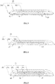
FIG. 1 is a cross-sectional view of a display device according to a first embodiment of the present disclosure. -
FIG. 2 is a top view of the display device according to the first embodiment of the present disclosure. -
FIG. 3 is a cross-sectional view of a display device according to a second embodiment of the present disclosure. -
FIG. 4 is a cross-sectional view of a display device according to a third embodiment of the present disclosure. -
FIG. 5 is a cross-sectional view of a display device according to a fourth embodiment of the present disclosure. - Description of the reference numerals:
10- light-emitting display layer, 20- planarization layer, 30- encapsulation layer, 301-inorganic layer, 302- organic layer, 40- groove, and 50- insulated layer. - Referring to
FIG. 1 and FIG. 2 , a display device is provided according to an embodiment of the present disclosure, including a light-emitting display layer 10, aplanarization layer 20, and anencapsulation layer 30. Theplanarization layer 20 is provided with at least one closedcircular groove 40, and a projection of a closed circle formed by thegroove 40 on a plane on which the light-emittingdisplay layer 10 is located is completely placed outside the light-emittingdisplay layer 10 and surrounds the light-emitting display layer 10. - In the display device described above, the closed
groove 40 can effectively block the outside moisture or oxygen from seeping through a contact surface between theencapsulation layer 30 and theplanarization layer 20 and making contact with the light-emittingdisplay layer 10, thereby improving the moisture-blocking and oxygen-blocking performance of the device and effectively improving the encapsulation effect, to increase the service life of the display device. Experiments prove that the display device of the present technical solution can light up for 1,230 hours under a condition of high temperature and high humidity, which considerably exceeds 480 hours for a display device without thegroove 40. - Preferably, the
encapsulation layer 30 includes aninorganic layer 301. A projection of a boundary of theplanarization layer 20 on the plane on which the light-emittingdisplay layer 10 is located is placed inside a projection of a boundary of theinorganic layer 301 on the plane on which the light-emitting display layer 10 is located, and does not coincide with the projection of the boundary of theinorganic layer 301. Theinorganic layer 301 has good moisture-blocking and oxygen-blocking performances for blocking the contact of the external moisture or oxygen with the light-emittingdisplay layer 10 to protect the light-emittingdisplay layer 10. By covering theplanarization layer 20 with theinorganic layer 301 completely, moisture or oxygen is better prevented from entering the inside of theencapsulation layer 30 through theplanarization layer 20. Preferably, a distance D between the projection of thegroove 40 on the plane on which the light-emitting display layer 10 is located and the projection of the boundary of theinorganic layer 301 on the plane on which the light-emitting display layer 10 is located is between 1 micrometer and 3,000 micrometers. The non-display area of the display device is minimized as much as possible while ensuring that theplanarization layer 20 is completely covered with theinorganic layer 301, so that the effective display area of the display device is sufficiently enlarged. - Preferably, referring to
FIG. 3 , an insulatedlayer 50 is further included, to which an edge of theinorganic layer 301 is connected. The insulatedlayer 50 is used for isolating theplanarization layer 20 from a driving element of the display device to achieve a protect effect on the driving element. By connecting the edge of theinorganic layer 301 to theinsulated layer 50, on one hand theplanarization layer 20 can be more completely encapsulated, and on the other hand theinorganic layer 301 has a better performance to be combined with theinsulated layer 50, to realize a more reliable encapsulation effect more easily. - Preferably, the
encapsulation layer 30 further includes anorganic layer 302 laminated with theinorganic layer 301 adjacently. Theorganic layer 302 has good flexibility for preventing theinorganic layer 301 from cracking during bending. More preferably, a projection of theorganic layer 302 on the plane on which the light-emittingdisplay layer 10 is located can completely cover the light-emittingdisplay layer 10 and is placed inside the projection of the closed circle formed by thegroove 40 on the plane on which the light-emittingdisplay layer 10 is located. A distance d between the projection of thegroove 40 on the plane on which the light-emittingdisplay layer 10 is located and a projection of a boundary of theorganic layer 302 on the plane on which the light-emitting display layer 10 is located is between 1 micrometer and 1,000 micrometers. According to this configuration, when the organic layer is disposed inside the groove, the formation of the organic layer and the inorganic layer does not have any sags because of the presence of the groove, thereby further ensuring the uniformity of the thicknesses of theorganic layer 302 and theinorganic layer 301. - Preferably, the
groove 40 extends through theplanarization layer 20 in a thickness direction of theplanarization layer 20. This configuration of thegroove 40 completely blocks the transmission path of the moisture or oxygen in theplanarization layer 20. - Referring to
FIG. 4 , in another embodiment, thegroove 40 also may not completely extend through theplanarization layer 20, and form an opening on theplanarization layer 20. The opening faces toward theencapsulation layer 30. In actual manufacturing, if theplanarization layer 20 is processed to have a groove completely extending through theplanarization layer 20, it is difficult to ensure the entirety of the film structure underneath theplanarization layer 20, and the device performance may be affected consequently. In contrast, if thegroove 40 is made not to completely extend through theplanarization layer 20, it can avoid the damage to the film layer underneath theplanarization layer 20 during the formation of thegroove 40 caused by the low process precision, resulting in a lower requirement for the processing of theplanarization layer 20, which is easier to realize. - Preferably, the
groove 40 has a depth of 30% or more of a thickness of theplanarization layer 20, and this depth of thegroove 40 is most controllable during the actual process. - Preferably, the
groove 40 has a width between 1 micrometer and 100 micrometers. Under the condition of a constant depth, the larger the width of thegroove 40, the larger the volume of thegroove 40 is, i.e. the larger the retention space in the process of diffusion and permeation of moisture or oxygen into the device, the better moisture-blocking and oxygen-blocking performances of the device are. However, the wider the width of thegroove 40, the more easily sags on theencapsulation layer 30 covering thegroove 40 are formed, which affects the flatness of the device. Thus, this width setting of the groove not only ensures the moisture-blocking and gas-blocking performance of the device, but also does not affect the overall flatness of the display device. - In the embodiments of
FIG. 1 to FIG. 3 , theencapsulation layer 30 is disposed in a laminated manner with the light-emittingdisplay layer 10 and theplanarization layer 20, and theencapsulation layer 30 includes twoinorganic layers 301 and oneorganic layer 302. Theorganic layer 302 is laminated between the twoinorganic layers 301, and the edge of theorganic layer 302 does not exceed the edges of theinorganic layers 301. - Referring to
FIG. 5 , in another embodiment, theencapsulation layer 20 includes threeinorganic layers 301 and twoorganic layers 302 alternately laminated to further block diffusion and penetration of moisture or a harmful gas in theencapsulation layer 20, thereby improving the moisture-blocking and gas-blocking performances of the flexible device, as well as increasing the bending life of the flexible device. - The above-mentioned embodiments are merely illustrative of several embodiments of the present disclosure, and the description thereof is more specific and detailed, but is not to be construed as limiting the scope of the present disclosure. It should be noted that a number of variations and modifications may be made by those skilled in the art without departing from the spirit and scope of the disclosure, which belong to the protection scope of the present disclosure. Therefore, the scope of the disclosure should be determined by the appended claims.
Claims (12)
- A display device, characterized in that, the display device comprises a light-emitting display layer, a planarization layer and an encapsulation layer stacked in sequence,
wherein the planarization layer is provided with at least one closed circular groove, and a projection of a closed circle formed by the groove on a plane on which the light-emitting display layer is located is completely placed outside the light-emitting display layer and surrounds the light-emitting display layer. - The display device of claim 1, characterized in that the encapsulation layer comprises an inorganic layer, a projection of a boundary of the planarization layer on the plane on which the light-emitting display layer is located is placed inside a projection of a boundary of the inorganic layer on the plane on which the light-emitting display is located, and does not overlap with the projection of the boundary of the inorganic layer on the plane on which the light-emitting display layer is located.
- The display device of claim 2, characterized in that a distance between a projection of the groove on the plane on which the light-emitting display layer is located and the projection of the boundary of the inorganic layer on the plane on which the light-emitting display layer is located is between 1 micrometer and 3,000 micrometers.
- The display device of claim 2, characterized in that the display device further comprises an insulated layer, an edge of the inorganic layer being connected to the insulated layer.
- The display device of claim 2, characterized in that the insulated layer isolates the planarization layer from a driving element of the display device.
- The display device of claim 1, characterized in that the encapsulation layer comprises an organic layer, a projection of the organic layer on the plane on which the light-emitting display layer is located completely covers the light-emitting display layer and is located inside the projection of the closed circle formed by the groove on the plane on which the light-emitting display layer is located.
- The display device of claim 6, characterized in that a distance between a projection of the groove on the plane on which the light-emitting display layer is located and a projection of a boundary of the organic layer on the plane on which the light-emitting display layer is located is between 1 micrometer and 1,000 micrometers.
- The display device of claim 6, characterized in that the encapsulation layer further comprises a plurality of inorganic layers laminated alternately with the organic layer, an edge of the organic layer not exceeding an edge of the inorganic layer.
- The display device of claim 1, characterized in that the groove extends through the planarization layer in a thickness direction of the planarization layer.
- The display device of claim 1, characterized in that the groove does not extend through the planarization layer completely and forms an opening on the planarization layer, the opening facing toward the encapsulation layer.
- The display device of claim 10, characterized in that the groove has a depth of 30% or more of a thickness of the planarization layer.
- The display device of claim 1, characterized in that the groove has a width between 1 micrometer and 100 micrometers.
Applications Claiming Priority (2)
| Application Number | Priority Date | Filing Date | Title |
|---|---|---|---|
| CN201721592396.9U CN207705199U (en) | 2017-11-24 | 2017-11-24 | Display device |
| PCT/CN2018/085177 WO2019100661A1 (en) | 2017-11-24 | 2018-04-28 | Display device |
Publications (3)
| Publication Number | Publication Date |
|---|---|
| EP3637470A1 true EP3637470A1 (en) | 2020-04-15 |
| EP3637470A4 EP3637470A4 (en) | 2020-08-05 |
| EP3637470B1 EP3637470B1 (en) | 2022-11-30 |
Family
ID=63023472
Family Applications (1)
| Application Number | Title | Priority Date | Filing Date |
|---|---|---|---|
| EP18881323.2A Active EP3637470B1 (en) | 2017-11-24 | 2018-04-28 | Display device |
Country Status (7)
| Country | Link |
|---|---|
| US (1) | US11289676B2 (en) |
| EP (1) | EP3637470B1 (en) |
| JP (1) | JP6960476B2 (en) |
| KR (1) | KR102407515B1 (en) |
| CN (1) | CN207705199U (en) |
| TW (1) | TWM564824U (en) |
| WO (1) | WO2019100661A1 (en) |
Cited By (1)
| Publication number | Priority date | Publication date | Assignee | Title |
|---|---|---|---|---|
| US11903273B2 (en) | 2020-07-27 | 2024-02-13 | Chengdu Boe Optoelectronics Technology Co., Ltd. | Display substrate and display device |
Families Citing this family (1)
| Publication number | Priority date | Publication date | Assignee | Title |
|---|---|---|---|---|
| CN110176551B (en) * | 2019-06-28 | 2022-04-05 | 京东方科技集团股份有限公司 | Organic light emitting diode display substrate, method and display device |
Family Cites Families (32)
| Publication number | Priority date | Publication date | Assignee | Title |
|---|---|---|---|---|
| JP4518747B2 (en) | 2003-05-08 | 2010-08-04 | 三洋電機株式会社 | Organic EL display device |
| KR100623338B1 (en) * | 2004-10-21 | 2006-09-19 | 엘지전자 주식회사 | Organic electroluminescent device and method of manufacturing same |
| EP1655790B1 (en) * | 2004-10-21 | 2010-08-04 | LG Display Co., Ltd. | Organic electroluminescent device and method of manufacturing the same |
| JP4458379B2 (en) | 2007-12-14 | 2010-04-28 | キヤノン株式会社 | Organic EL display device |
| US7936122B2 (en) | 2007-12-14 | 2011-05-03 | Canon Kabushiki Kaisha | Organic EL display apparatus |
| JP2009266922A (en) | 2008-04-23 | 2009-11-12 | Canon Inc | Organic light-emitting device |
| JP2009283242A (en) | 2008-05-21 | 2009-12-03 | Canon Inc | Organic el display device |
| JP5424738B2 (en) * | 2009-06-23 | 2014-02-26 | キヤノン株式会社 | Display device |
| JP2013123000A (en) * | 2011-12-12 | 2013-06-20 | Sony Corp | Solid-state image pickup device and method for manufacturing the same |
| EP2685515A1 (en) | 2012-07-12 | 2014-01-15 | Nederlandse Organisatie voor toegepast -natuurwetenschappelijk onderzoek TNO | Method and system for dividing a barrier foil |
| KR101994227B1 (en) * | 2012-12-07 | 2019-09-30 | 엘지디스플레이 주식회사 | Organic light emitting diode device and method for fabricating the same |
| JP6391917B2 (en) * | 2013-07-03 | 2018-09-19 | 株式会社ジャパンディスプレイ | Light emitting element display device and manufacturing method thereof |
| CN203883009U (en) | 2014-05-29 | 2014-10-15 | 京东方科技集团股份有限公司 | Oled display panel |
| KR102253531B1 (en) | 2014-07-25 | 2021-05-18 | 삼성디스플레이 주식회사 | Display device and method for manufacturing the same |
| KR102250048B1 (en) * | 2014-09-16 | 2021-05-11 | 삼성디스플레이 주식회사 | Organic light emitting display device |
| TWI533055B (en) | 2014-09-30 | 2016-05-11 | 群創光電股份有限公司 | Display panel |
| KR102317393B1 (en) * | 2014-10-17 | 2021-10-25 | 엘지디스플레이 주식회사 | Organic light emitting display device and method of manufacturing the same |
| KR20160076688A (en) * | 2014-12-23 | 2016-07-01 | 엘지디스플레이 주식회사 | Organic light emitting display device and method of manufacturing the same |
| KR102462424B1 (en) * | 2014-12-30 | 2022-11-03 | 삼성디스플레이 주식회사 | Display Device |
| KR102396296B1 (en) * | 2015-03-06 | 2022-05-11 | 삼성디스플레이 주식회사 | Organic light-emitting display apparatus and manufacturing the same |
| KR102422279B1 (en) * | 2015-10-22 | 2022-07-19 | 삼성디스플레이 주식회사 | Organic light emitting diode display and manufacturing method thereof |
| JP6605919B2 (en) * | 2015-11-05 | 2019-11-13 | 株式会社ジャパンディスプレイ | Display device manufacturing method and display device |
| KR102446425B1 (en) * | 2015-11-17 | 2022-09-23 | 삼성디스플레이 주식회사 | Display device and method of manufacturing display device |
| CN205452362U (en) | 2015-12-31 | 2016-08-10 | 固安翌光科技有限公司 | Thin film packaging structure |
| JP6634290B2 (en) * | 2016-01-04 | 2020-01-22 | 株式会社ジャパンディスプレイ | Organic EL display |
| CN105449118B (en) | 2016-01-04 | 2017-12-08 | 京东方科技集团股份有限公司 | A kind of encapsulating structure of OLED, display device and method for packing |
| KR102567547B1 (en) * | 2016-03-22 | 2023-08-17 | 삼성디스플레이 주식회사 | Display device |
| KR102421577B1 (en) * | 2016-04-05 | 2022-07-18 | 삼성디스플레이 주식회사 | Display device |
| CN108281458B (en) * | 2017-01-03 | 2020-09-22 | 昆山工研院新型平板显示技术中心有限公司 | Flexible OLED display device and preparation method thereof |
| CN106876428B (en) * | 2017-02-03 | 2019-10-08 | 上海天马微电子有限公司 | flexible display panel, manufacturing method thereof and display device |
| WO2018179035A1 (en) * | 2017-03-27 | 2018-10-04 | シャープ株式会社 | Display device |
| JP2019079729A (en) * | 2017-10-26 | 2019-05-23 | 株式会社ジャパンディスプレイ | Display |
-
2017
- 2017-11-24 CN CN201721592396.9U patent/CN207705199U/en active Active
-
2018
- 2018-04-28 US US16/342,196 patent/US11289676B2/en active Active
- 2018-04-28 KR KR1020197038734A patent/KR102407515B1/en active Active
- 2018-04-28 JP JP2019567681A patent/JP6960476B2/en active Active
- 2018-04-28 WO PCT/CN2018/085177 patent/WO2019100661A1/en not_active Ceased
- 2018-04-28 EP EP18881323.2A patent/EP3637470B1/en active Active
- 2018-05-14 TW TW107206258U patent/TWM564824U/en unknown
Cited By (1)
| Publication number | Priority date | Publication date | Assignee | Title |
|---|---|---|---|---|
| US11903273B2 (en) | 2020-07-27 | 2024-02-13 | Chengdu Boe Optoelectronics Technology Co., Ltd. | Display substrate and display device |
Also Published As
| Publication number | Publication date |
|---|---|
| JP6960476B2 (en) | 2021-11-05 |
| CN207705199U (en) | 2018-08-07 |
| WO2019100661A1 (en) | 2019-05-31 |
| JP2020522863A (en) | 2020-07-30 |
| US20210328178A1 (en) | 2021-10-21 |
| KR102407515B1 (en) | 2022-06-10 |
| KR20200006131A (en) | 2020-01-17 |
| EP3637470B1 (en) | 2022-11-30 |
| TWM564824U (en) | 2018-08-01 |
| US11289676B2 (en) | 2022-03-29 |
| EP3637470A4 (en) | 2020-08-05 |
Similar Documents
| Publication | Publication Date | Title |
|---|---|---|
| USRE49770E1 (en) | Flexible display having a crack suppressing layer | |
| KR102367275B1 (en) | An organic light emitting display apparatus and the manufacturing method thereof | |
| CN109410758B (en) | Transparent display device | |
| KR102362819B1 (en) | Flexible display device | |
| US11101437B2 (en) | Display substrate motherboard, display substrate and display device | |
| US10962814B2 (en) | Flexible display device | |
| US8981643B2 (en) | Electroluminescent display panel | |
| CN105355645B (en) | A flexible display panel, its manufacturing method, and display device | |
| CN114784016A (en) | Display panel and display device | |
| KR20200037765A (en) | Flexible display device and manufacturing method thereof | |
| CN106229321A (en) | Array substrate and display panel | |
| CN108538899B (en) | Display panel and display screen | |
| WO2020211288A1 (en) | Display panel and display device | |
| CN113809133B (en) | Display panels and display devices | |
| EP3660939B1 (en) | Display device and packaging method therefor | |
| CN114287063A (en) | Display substrate and display device | |
| US11289676B2 (en) | Display device having a closed circular groove planarization layer | |
| WO2020252944A1 (en) | Light-emitting panel and display apparatus | |
| KR20140084919A (en) | Organic light emitting diode display device and method of manufacturing the same | |
| TWI607552B (en) | Pixel array substrate, display panel, and master thereof | |
| CN107342363A (en) | Display base plate and preparation method thereof | |
| CN111403627B (en) | Display panel, manufacturing method thereof and display device | |
| KR102350896B1 (en) | Organic light emitting display device and method of manufacturing the same | |
| JPWO2013111218A1 (en) | Element structure and method for manufacturing element structure | |
| US7764015B2 (en) | Display device |
Legal Events
| Date | Code | Title | Description |
|---|---|---|---|
| STAA | Information on the status of an ep patent application or granted ep patent |
Free format text: STATUS: THE INTERNATIONAL PUBLICATION HAS BEEN MADE |
|
| PUAI | Public reference made under article 153(3) epc to a published international application that has entered the european phase |
Free format text: ORIGINAL CODE: 0009012 |
|
| STAA | Information on the status of an ep patent application or granted ep patent |
Free format text: STATUS: REQUEST FOR EXAMINATION WAS MADE |
|
| 17P | Request for examination filed |
Effective date: 20200110 |
|
| AK | Designated contracting states |
Kind code of ref document: A1 Designated state(s): AL AT BE BG CH CY CZ DE DK EE ES FI FR GB GR HR HU IE IS IT LI LT LU LV MC MK MT NL NO PL PT RO RS SE SI SK SM TR |
|
| AX | Request for extension of the european patent |
Extension state: BA ME |
|
| A4 | Supplementary search report drawn up and despatched |
Effective date: 20200707 |
|
| RIC1 | Information provided on ipc code assigned before grant |
Ipc: H01L 51/52 20060101ALI20200701BHEP Ipc: H01L 27/32 20060101AFI20200701BHEP |
|
| DAV | Request for validation of the european patent (deleted) | ||
| DAX | Request for extension of the european patent (deleted) | ||
| GRAP | Despatch of communication of intention to grant a patent |
Free format text: ORIGINAL CODE: EPIDOSNIGR1 |
|
| STAA | Information on the status of an ep patent application or granted ep patent |
Free format text: STATUS: GRANT OF PATENT IS INTENDED |
|
| INTG | Intention to grant announced |
Effective date: 20220905 |
|
| GRAS | Grant fee paid |
Free format text: ORIGINAL CODE: EPIDOSNIGR3 |
|
| GRAA | (expected) grant |
Free format text: ORIGINAL CODE: 0009210 |
|
| STAA | Information on the status of an ep patent application or granted ep patent |
Free format text: STATUS: THE PATENT HAS BEEN GRANTED |
|
| REG | Reference to a national code |
Ref country code: DE Ref legal event code: R079 Ref document number: 602018043824 Country of ref document: DE Free format text: PREVIOUS MAIN CLASS: H01L0027320000 Ipc: H10K0059000000 |
|
| AK | Designated contracting states |
Kind code of ref document: B1 Designated state(s): AL AT BE BG CH CY CZ DE DK EE ES FI FR GB GR HR HU IE IS IT LI LT LU LV MC MK MT NL NO PL PT RO RS SE SI SK SM TR |
|
| REG | Reference to a national code |
Ref country code: CH Ref legal event code: EP Ref country code: GB Ref legal event code: FG4D |
|
| REG | Reference to a national code |
Ref country code: AT Ref legal event code: REF Ref document number: 1535342 Country of ref document: AT Kind code of ref document: T Effective date: 20221215 Ref country code: DE Ref legal event code: R096 Ref document number: 602018043824 Country of ref document: DE |
|
| REG | Reference to a national code |
Ref country code: IE Ref legal event code: FG4D |
|
| REG | Reference to a national code |
Ref country code: LT Ref legal event code: MG9D |
|
| REG | Reference to a national code |
Ref country code: NL Ref legal event code: MP Effective date: 20221130 |
|
| PG25 | Lapsed in a contracting state [announced via postgrant information from national office to epo] |
Ref country code: SE Free format text: LAPSE BECAUSE OF FAILURE TO SUBMIT A TRANSLATION OF THE DESCRIPTION OR TO PAY THE FEE WITHIN THE PRESCRIBED TIME-LIMIT Effective date: 20221130 Ref country code: PT Free format text: LAPSE BECAUSE OF FAILURE TO SUBMIT A TRANSLATION OF THE DESCRIPTION OR TO PAY THE FEE WITHIN THE PRESCRIBED TIME-LIMIT Effective date: 20230331 Ref country code: NO Free format text: LAPSE BECAUSE OF FAILURE TO SUBMIT A TRANSLATION OF THE DESCRIPTION OR TO PAY THE FEE WITHIN THE PRESCRIBED TIME-LIMIT Effective date: 20230228 Ref country code: LT Free format text: LAPSE BECAUSE OF FAILURE TO SUBMIT A TRANSLATION OF THE DESCRIPTION OR TO PAY THE FEE WITHIN THE PRESCRIBED TIME-LIMIT Effective date: 20221130 Ref country code: FI Free format text: LAPSE BECAUSE OF FAILURE TO SUBMIT A TRANSLATION OF THE DESCRIPTION OR TO PAY THE FEE WITHIN THE PRESCRIBED TIME-LIMIT Effective date: 20221130 Ref country code: ES Free format text: LAPSE BECAUSE OF FAILURE TO SUBMIT A TRANSLATION OF THE DESCRIPTION OR TO PAY THE FEE WITHIN THE PRESCRIBED TIME-LIMIT Effective date: 20221130 |
|
| REG | Reference to a national code |
Ref country code: AT Ref legal event code: MK05 Ref document number: 1535342 Country of ref document: AT Kind code of ref document: T Effective date: 20221130 |
|
| PG25 | Lapsed in a contracting state [announced via postgrant information from national office to epo] |
Ref country code: RS Free format text: LAPSE BECAUSE OF FAILURE TO SUBMIT A TRANSLATION OF THE DESCRIPTION OR TO PAY THE FEE WITHIN THE PRESCRIBED TIME-LIMIT Effective date: 20221130 Ref country code: PL Free format text: LAPSE BECAUSE OF FAILURE TO SUBMIT A TRANSLATION OF THE DESCRIPTION OR TO PAY THE FEE WITHIN THE PRESCRIBED TIME-LIMIT Effective date: 20221130 Ref country code: LV Free format text: LAPSE BECAUSE OF FAILURE TO SUBMIT A TRANSLATION OF THE DESCRIPTION OR TO PAY THE FEE WITHIN THE PRESCRIBED TIME-LIMIT Effective date: 20221130 Ref country code: IS Free format text: LAPSE BECAUSE OF FAILURE TO SUBMIT A TRANSLATION OF THE DESCRIPTION OR TO PAY THE FEE WITHIN THE PRESCRIBED TIME-LIMIT Effective date: 20230330 Ref country code: HR Free format text: LAPSE BECAUSE OF FAILURE TO SUBMIT A TRANSLATION OF THE DESCRIPTION OR TO PAY THE FEE WITHIN THE PRESCRIBED TIME-LIMIT Effective date: 20221130 Ref country code: GR Free format text: LAPSE BECAUSE OF FAILURE TO SUBMIT A TRANSLATION OF THE DESCRIPTION OR TO PAY THE FEE WITHIN THE PRESCRIBED TIME-LIMIT Effective date: 20230301 |
|
| PG25 | Lapsed in a contracting state [announced via postgrant information from national office to epo] |
Ref country code: NL Free format text: LAPSE BECAUSE OF FAILURE TO SUBMIT A TRANSLATION OF THE DESCRIPTION OR TO PAY THE FEE WITHIN THE PRESCRIBED TIME-LIMIT Effective date: 20221130 |
|
| P01 | Opt-out of the competence of the unified patent court (upc) registered |
Effective date: 20230526 |
|
| PG25 | Lapsed in a contracting state [announced via postgrant information from national office to epo] |
Ref country code: SM Free format text: LAPSE BECAUSE OF FAILURE TO SUBMIT A TRANSLATION OF THE DESCRIPTION OR TO PAY THE FEE WITHIN THE PRESCRIBED TIME-LIMIT Effective date: 20221130 Ref country code: RO Free format text: LAPSE BECAUSE OF FAILURE TO SUBMIT A TRANSLATION OF THE DESCRIPTION OR TO PAY THE FEE WITHIN THE PRESCRIBED TIME-LIMIT Effective date: 20221130 Ref country code: EE Free format text: LAPSE BECAUSE OF FAILURE TO SUBMIT A TRANSLATION OF THE DESCRIPTION OR TO PAY THE FEE WITHIN THE PRESCRIBED TIME-LIMIT Effective date: 20221130 Ref country code: DK Free format text: LAPSE BECAUSE OF FAILURE TO SUBMIT A TRANSLATION OF THE DESCRIPTION OR TO PAY THE FEE WITHIN THE PRESCRIBED TIME-LIMIT Effective date: 20221130 Ref country code: CZ Free format text: LAPSE BECAUSE OF FAILURE TO SUBMIT A TRANSLATION OF THE DESCRIPTION OR TO PAY THE FEE WITHIN THE PRESCRIBED TIME-LIMIT Effective date: 20221130 Ref country code: AT Free format text: LAPSE BECAUSE OF FAILURE TO SUBMIT A TRANSLATION OF THE DESCRIPTION OR TO PAY THE FEE WITHIN THE PRESCRIBED TIME-LIMIT Effective date: 20221130 |
|
| PG25 | Lapsed in a contracting state [announced via postgrant information from national office to epo] |
Ref country code: SK Free format text: LAPSE BECAUSE OF FAILURE TO SUBMIT A TRANSLATION OF THE DESCRIPTION OR TO PAY THE FEE WITHIN THE PRESCRIBED TIME-LIMIT Effective date: 20221130 Ref country code: AL Free format text: LAPSE BECAUSE OF FAILURE TO SUBMIT A TRANSLATION OF THE DESCRIPTION OR TO PAY THE FEE WITHIN THE PRESCRIBED TIME-LIMIT Effective date: 20221130 |
|
| REG | Reference to a national code |
Ref country code: DE Ref legal event code: R097 Ref document number: 602018043824 Country of ref document: DE |
|
| PLBE | No opposition filed within time limit |
Free format text: ORIGINAL CODE: 0009261 |
|
| STAA | Information on the status of an ep patent application or granted ep patent |
Free format text: STATUS: NO OPPOSITION FILED WITHIN TIME LIMIT |
|
| 26N | No opposition filed |
Effective date: 20230831 |
|
| PG25 | Lapsed in a contracting state [announced via postgrant information from national office to epo] |
Ref country code: SI Free format text: LAPSE BECAUSE OF FAILURE TO SUBMIT A TRANSLATION OF THE DESCRIPTION OR TO PAY THE FEE WITHIN THE PRESCRIBED TIME-LIMIT Effective date: 20221130 |
|
| REG | Reference to a national code |
Ref country code: CH Ref legal event code: PL |
|
| PG25 | Lapsed in a contracting state [announced via postgrant information from national office to epo] |
Ref country code: LU Free format text: LAPSE BECAUSE OF NON-PAYMENT OF DUE FEES Effective date: 20230428 |
|
| REG | Reference to a national code |
Ref country code: BE Ref legal event code: MM Effective date: 20230430 |
|
| PG25 | Lapsed in a contracting state [announced via postgrant information from national office to epo] |
Ref country code: MC Free format text: LAPSE BECAUSE OF FAILURE TO SUBMIT A TRANSLATION OF THE DESCRIPTION OR TO PAY THE FEE WITHIN THE PRESCRIBED TIME-LIMIT Effective date: 20221130 |
|
| PG25 | Lapsed in a contracting state [announced via postgrant information from national office to epo] |
Ref country code: MC Free format text: LAPSE BECAUSE OF FAILURE TO SUBMIT A TRANSLATION OF THE DESCRIPTION OR TO PAY THE FEE WITHIN THE PRESCRIBED TIME-LIMIT Effective date: 20221130 Ref country code: LI Free format text: LAPSE BECAUSE OF NON-PAYMENT OF DUE FEES Effective date: 20230430 Ref country code: CH Free format text: LAPSE BECAUSE OF NON-PAYMENT OF DUE FEES Effective date: 20230430 |
|
| REG | Reference to a national code |
Ref country code: IE Ref legal event code: MM4A |
|
| PG25 | Lapsed in a contracting state [announced via postgrant information from national office to epo] |
Ref country code: BE Free format text: LAPSE BECAUSE OF NON-PAYMENT OF DUE FEES Effective date: 20230430 |
|
| PG25 | Lapsed in a contracting state [announced via postgrant information from national office to epo] |
Ref country code: IE Free format text: LAPSE BECAUSE OF NON-PAYMENT OF DUE FEES Effective date: 20230428 |
|
| PG25 | Lapsed in a contracting state [announced via postgrant information from national office to epo] |
Ref country code: IE Free format text: LAPSE BECAUSE OF NON-PAYMENT OF DUE FEES Effective date: 20230428 |
|
| PG25 | Lapsed in a contracting state [announced via postgrant information from national office to epo] |
Ref country code: IT Free format text: LAPSE BECAUSE OF FAILURE TO SUBMIT A TRANSLATION OF THE DESCRIPTION OR TO PAY THE FEE WITHIN THE PRESCRIBED TIME-LIMIT Effective date: 20221130 |
|
| PG25 | Lapsed in a contracting state [announced via postgrant information from national office to epo] |
Ref country code: BG Free format text: LAPSE BECAUSE OF FAILURE TO SUBMIT A TRANSLATION OF THE DESCRIPTION OR TO PAY THE FEE WITHIN THE PRESCRIBED TIME-LIMIT Effective date: 20221130 |
|
| PG25 | Lapsed in a contracting state [announced via postgrant information from national office to epo] |
Ref country code: BG Free format text: LAPSE BECAUSE OF FAILURE TO SUBMIT A TRANSLATION OF THE DESCRIPTION OR TO PAY THE FEE WITHIN THE PRESCRIBED TIME-LIMIT Effective date: 20221130 |
|
| PGFP | Annual fee paid to national office [announced via postgrant information from national office to epo] |
Ref country code: DE Payment date: 20250411 Year of fee payment: 8 |
|
| PGFP | Annual fee paid to national office [announced via postgrant information from national office to epo] |
Ref country code: GB Payment date: 20250417 Year of fee payment: 8 |
|
| PGFP | Annual fee paid to national office [announced via postgrant information from national office to epo] |
Ref country code: FR Payment date: 20250429 Year of fee payment: 8 |
|
| PG25 | Lapsed in a contracting state [announced via postgrant information from national office to epo] |
Ref country code: CY Free format text: LAPSE BECAUSE OF FAILURE TO SUBMIT A TRANSLATION OF THE DESCRIPTION OR TO PAY THE FEE WITHIN THE PRESCRIBED TIME-LIMIT; INVALID AB INITIO Effective date: 20180428 |
|
| PG25 | Lapsed in a contracting state [announced via postgrant information from national office to epo] |
Ref country code: HU Free format text: LAPSE BECAUSE OF FAILURE TO SUBMIT A TRANSLATION OF THE DESCRIPTION OR TO PAY THE FEE WITHIN THE PRESCRIBED TIME-LIMIT; INVALID AB INITIO Effective date: 20180428 |
|
| PG25 | Lapsed in a contracting state [announced via postgrant information from national office to epo] |
Ref country code: TR Free format text: LAPSE BECAUSE OF FAILURE TO SUBMIT A TRANSLATION OF THE DESCRIPTION OR TO PAY THE FEE WITHIN THE PRESCRIBED TIME-LIMIT Effective date: 20221130 |