EP3637444A1 - Voltage regulator module - Google Patents
Voltage regulator module Download PDFInfo
- Publication number
- EP3637444A1 EP3637444A1 EP19201084.1A EP19201084A EP3637444A1 EP 3637444 A1 EP3637444 A1 EP 3637444A1 EP 19201084 A EP19201084 A EP 19201084A EP 3637444 A1 EP3637444 A1 EP 3637444A1
- Authority
- EP
- European Patent Office
- Prior art keywords
- circuit board
- printed circuit
- voltage regulator
- regulator module
- assembly
- Prior art date
- Legal status (The legal status is an assumption and is not a legal conclusion. Google has not performed a legal analysis and makes no representation as to the accuracy of the status listed.)
- Withdrawn
Links
Images





Classifications
-
- H—ELECTRICITY
- H01—ELECTRIC ELEMENTS
- H01F—MAGNETS; INDUCTANCES; TRANSFORMERS; SELECTION OF MATERIALS FOR THEIR MAGNETIC PROPERTIES
- H01F27/00—Details of transformers or inductances, in general
- H01F27/28—Coils; Windings; Conductive connections
- H01F27/2804—Printed windings
-
- H—ELECTRICITY
- H01—ELECTRIC ELEMENTS
- H01F—MAGNETS; INDUCTANCES; TRANSFORMERS; SELECTION OF MATERIALS FOR THEIR MAGNETIC PROPERTIES
- H01F17/00—Fixed inductances of the signal type
- H01F17/04—Fixed inductances of the signal type with magnetic core
- H01F17/06—Fixed inductances of the signal type with magnetic core with core substantially closed in itself, e.g. toroid
-
- G—PHYSICS
- G05—CONTROLLING; REGULATING
- G05F—SYSTEMS FOR REGULATING ELECTRIC OR MAGNETIC VARIABLES
- G05F1/00—Automatic systems in which deviations of an electric quantity from one or more predetermined values are detected at the output of the system and fed back to a device within the system to restore the detected quantity to its predetermined value or values, i.e. retroactive systems
- G05F1/10—Regulating voltage or current
- G05F1/46—Regulating voltage or current wherein the variable actually regulated by the final control device is DC
- G05F1/56—Regulating voltage or current wherein the variable actually regulated by the final control device is DC using semiconductor devices in series with the load as final control devices
- G05F1/575—Regulating voltage or current wherein the variable actually regulated by the final control device is DC using semiconductor devices in series with the load as final control devices characterised by the feedback circuit
-
- G—PHYSICS
- G06—COMPUTING OR CALCULATING; COUNTING
- G06F—ELECTRIC DIGITAL DATA PROCESSING
- G06F1/00—Details not covered by groups G06F3/00 - G06F13/00 and G06F21/00
- G06F1/16—Constructional details or arrangements
- G06F1/18—Packaging or power distribution
- G06F1/183—Internal mounting support structures, e.g. for supporting printed circuit boards
-
- H—ELECTRICITY
- H01—ELECTRIC ELEMENTS
- H01F—MAGNETS; INDUCTANCES; TRANSFORMERS; SELECTION OF MATERIALS FOR THEIR MAGNETIC PROPERTIES
- H01F17/00—Fixed inductances of the signal type
- H01F17/04—Fixed inductances of the signal type with magnetic core
-
- H—ELECTRICITY
- H01—ELECTRIC ELEMENTS
- H01F—MAGNETS; INDUCTANCES; TRANSFORMERS; SELECTION OF MATERIALS FOR THEIR MAGNETIC PROPERTIES
- H01F27/00—Details of transformers or inductances, in general
- H01F27/02—Casings
-
- H—ELECTRICITY
- H01—ELECTRIC ELEMENTS
- H01F—MAGNETS; INDUCTANCES; TRANSFORMERS; SELECTION OF MATERIALS FOR THEIR MAGNETIC PROPERTIES
- H01F27/00—Details of transformers or inductances, in general
- H01F27/24—Magnetic cores
-
- H—ELECTRICITY
- H01—ELECTRIC ELEMENTS
- H01F—MAGNETS; INDUCTANCES; TRANSFORMERS; SELECTION OF MATERIALS FOR THEIR MAGNETIC PROPERTIES
- H01F27/00—Details of transformers or inductances, in general
- H01F27/28—Coils; Windings; Conductive connections
- H01F27/29—Terminals; Tapping arrangements for signal inductances
- H01F27/292—Surface mounted devices
-
- H—ELECTRICITY
- H01—ELECTRIC ELEMENTS
- H01R—ELECTRICALLY-CONDUCTIVE CONNECTIONS; STRUCTURAL ASSOCIATIONS OF A PLURALITY OF MUTUALLY-INSULATED ELECTRICAL CONNECTING ELEMENTS; COUPLING DEVICES; CURRENT COLLECTORS
- H01R12/00—Structural associations of a plurality of mutually-insulated electrical connecting elements, specially adapted for printed circuits, e.g. printed circuit boards [PCB], flat or ribbon cables, or like generally planar structures, e.g. terminal strips, terminal blocks; Coupling devices specially adapted for printed circuits, flat or ribbon cables, or like generally planar structures; Terminals specially adapted for contact with, or insertion into, printed circuits, flat or ribbon cables, or like generally planar structures
- H01R12/50—Fixed connections
- H01R12/51—Fixed connections for rigid printed circuits or like structures
- H01R12/52—Fixed connections for rigid printed circuits or like structures connecting to other rigid printed circuits or like structures
-
- H—ELECTRICITY
- H01—ELECTRIC ELEMENTS
- H01R—ELECTRICALLY-CONDUCTIVE CONNECTIONS; STRUCTURAL ASSOCIATIONS OF A PLURALITY OF MUTUALLY-INSULATED ELECTRICAL CONNECTING ELEMENTS; COUPLING DEVICES; CURRENT COLLECTORS
- H01R12/00—Structural associations of a plurality of mutually-insulated electrical connecting elements, specially adapted for printed circuits, e.g. printed circuit boards [PCB], flat or ribbon cables, or like generally planar structures, e.g. terminal strips, terminal blocks; Coupling devices specially adapted for printed circuits, flat or ribbon cables, or like generally planar structures; Terminals specially adapted for contact with, or insertion into, printed circuits, flat or ribbon cables, or like generally planar structures
- H01R12/50—Fixed connections
- H01R12/51—Fixed connections for rigid printed circuits or like structures
- H01R12/55—Fixed connections for rigid printed circuits or like structures characterised by the terminals
- H01R12/58—Fixed connections for rigid printed circuits or like structures characterised by the terminals terminals for insertion into holes
-
- H—ELECTRICITY
- H05—ELECTRIC TECHNIQUES NOT OTHERWISE PROVIDED FOR
- H05K—PRINTED CIRCUITS; CASINGS OR CONSTRUCTIONAL DETAILS OF ELECTRIC APPARATUS; MANUFACTURE OF ASSEMBLAGES OF ELECTRICAL COMPONENTS
- H05K1/00—Printed circuits
- H05K1/02—Details
- H05K1/0201—Thermal arrangements, e.g. for cooling, heating or preventing overheating
- H05K1/0203—Cooling of mounted components
-
- H—ELECTRICITY
- H05—ELECTRIC TECHNIQUES NOT OTHERWISE PROVIDED FOR
- H05K—PRINTED CIRCUITS; CASINGS OR CONSTRUCTIONAL DETAILS OF ELECTRIC APPARATUS; MANUFACTURE OF ASSEMBLAGES OF ELECTRICAL COMPONENTS
- H05K1/00—Printed circuits
- H05K1/02—Details
- H05K1/11—Printed elements for providing electric connections to or between printed circuits
- H05K1/111—Pads for surface mounting, e.g. lay-out
-
- H—ELECTRICITY
- H05—ELECTRIC TECHNIQUES NOT OTHERWISE PROVIDED FOR
- H05K—PRINTED CIRCUITS; CASINGS OR CONSTRUCTIONAL DETAILS OF ELECTRIC APPARATUS; MANUFACTURE OF ASSEMBLAGES OF ELECTRICAL COMPONENTS
- H05K1/00—Printed circuits
- H05K1/02—Details
- H05K1/11—Printed elements for providing electric connections to or between printed circuits
- H05K1/117—Pads along the edge of rigid circuit boards, e.g. for pluggable connectors
-
- H—ELECTRICITY
- H05—ELECTRIC TECHNIQUES NOT OTHERWISE PROVIDED FOR
- H05K—PRINTED CIRCUITS; CASINGS OR CONSTRUCTIONAL DETAILS OF ELECTRIC APPARATUS; MANUFACTURE OF ASSEMBLAGES OF ELECTRICAL COMPONENTS
- H05K1/00—Printed circuits
- H05K1/02—Details
- H05K1/14—Structural association of two or more printed circuits
- H05K1/145—Arrangements wherein electric components are disposed between and simultaneously connected to two planar printed circuit boards, e.g. Cordwood modules
-
- H—ELECTRICITY
- H05—ELECTRIC TECHNIQUES NOT OTHERWISE PROVIDED FOR
- H05K—PRINTED CIRCUITS; CASINGS OR CONSTRUCTIONAL DETAILS OF ELECTRIC APPARATUS; MANUFACTURE OF ASSEMBLAGES OF ELECTRICAL COMPONENTS
- H05K1/00—Printed circuits
- H05K1/16—Printed circuits incorporating printed electric components, e.g. printed resistors, capacitors or inductors
- H05K1/165—Printed circuits incorporating printed electric components, e.g. printed resistors, capacitors or inductors incorporating printed inductors
-
- H—ELECTRICITY
- H05—ELECTRIC TECHNIQUES NOT OTHERWISE PROVIDED FOR
- H05K—PRINTED CIRCUITS; CASINGS OR CONSTRUCTIONAL DETAILS OF ELECTRIC APPARATUS; MANUFACTURE OF ASSEMBLAGES OF ELECTRICAL COMPONENTS
- H05K1/00—Printed circuits
- H05K1/18—Printed circuits structurally associated with non-printed electric components
- H05K1/181—Printed circuits structurally associated with non-printed electric components associated with surface mounted components
-
- H—ELECTRICITY
- H05—ELECTRIC TECHNIQUES NOT OTHERWISE PROVIDED FOR
- H05K—PRINTED CIRCUITS; CASINGS OR CONSTRUCTIONAL DETAILS OF ELECTRIC APPARATUS; MANUFACTURE OF ASSEMBLAGES OF ELECTRICAL COMPONENTS
- H05K1/00—Printed circuits
- H05K1/18—Printed circuits structurally associated with non-printed electric components
- H05K1/182—Printed circuits structurally associated with non-printed electric components associated with components mounted in printed circuit boards [PCB], e.g. insert-mounted components [IMC]
- H05K1/185—Printed circuits structurally associated with non-printed electric components associated with components mounted in printed circuit boards [PCB], e.g. insert-mounted components [IMC] associated with components encapsulated in the insulating substrate of the PCBs; associated with components incorporated in internal layers of multilayer circuit boards
- H05K1/186—Printed circuits structurally associated with non-printed electric components associated with components mounted in printed circuit boards [PCB], e.g. insert-mounted components [IMC] associated with components encapsulated in the insulating substrate of the PCBs; associated with components incorporated in internal layers of multilayer circuit boards manufactured by mounting on or connecting to patterned circuits before or during embedding
-
- H—ELECTRICITY
- H05—ELECTRIC TECHNIQUES NOT OTHERWISE PROVIDED FOR
- H05K—PRINTED CIRCUITS; CASINGS OR CONSTRUCTIONAL DETAILS OF ELECTRIC APPARATUS; MANUFACTURE OF ASSEMBLAGES OF ELECTRICAL COMPONENTS
- H05K3/00—Apparatus or processes for manufacturing printed circuits
- H05K3/22—Secondary treatment of printed circuits
- H05K3/28—Applying non-metallic protective coatings
- H05K3/284—Applying non-metallic protective coatings for encapsulating mounted components
-
- H—ELECTRICITY
- H05—ELECTRIC TECHNIQUES NOT OTHERWISE PROVIDED FOR
- H05K—PRINTED CIRCUITS; CASINGS OR CONSTRUCTIONAL DETAILS OF ELECTRIC APPARATUS; MANUFACTURE OF ASSEMBLAGES OF ELECTRICAL COMPONENTS
- H05K7/00—Constructional details common to different types of electric apparatus
- H05K7/14—Mounting supporting structure in casing or on frame or rack
- H05K7/1422—Printed circuit boards receptacles, e.g. stacked structures, electronic circuit modules or box like frames
- H05K7/1427—Housings
-
- H—ELECTRICITY
- H05—ELECTRIC TECHNIQUES NOT OTHERWISE PROVIDED FOR
- H05K—PRINTED CIRCUITS; CASINGS OR CONSTRUCTIONAL DETAILS OF ELECTRIC APPARATUS; MANUFACTURE OF ASSEMBLAGES OF ELECTRICAL COMPONENTS
- H05K7/00—Constructional details common to different types of electric apparatus
- H05K7/20—Modifications to facilitate cooling, ventilating, or heating
- H05K7/2089—Modifications to facilitate cooling, ventilating, or heating for power electronics, e.g. for inverters for controlling motor
-
- H—ELECTRICITY
- H10—SEMICONDUCTOR DEVICES; ELECTRIC SOLID-STATE DEVICES NOT OTHERWISE PROVIDED FOR
- H10W—GENERIC PACKAGES, INTERCONNECTIONS, CONNECTORS OR OTHER CONSTRUCTIONAL DETAILS OF DEVICES COVERED BY CLASS H10
- H10W90/00—Package configurations
-
- H—ELECTRICITY
- H01—ELECTRIC ELEMENTS
- H01F—MAGNETS; INDUCTANCES; TRANSFORMERS; SELECTION OF MATERIALS FOR THEIR MAGNETIC PROPERTIES
- H01F17/00—Fixed inductances of the signal type
- H01F17/04—Fixed inductances of the signal type with magnetic core
- H01F17/06—Fixed inductances of the signal type with magnetic core with core substantially closed in itself, e.g. toroid
- H01F2017/067—Core with two or more holes to lead through conductor
-
- H—ELECTRICITY
- H02—GENERATION; CONVERSION OR DISTRIBUTION OF ELECTRIC POWER
- H02M—APPARATUS FOR CONVERSION BETWEEN AC AND AC, BETWEEN AC AND DC, OR BETWEEN DC AND DC, AND FOR USE WITH MAINS OR SIMILAR POWER SUPPLY SYSTEMS; CONVERSION OF DC OR AC INPUT POWER INTO SURGE OUTPUT POWER; CONTROL OR REGULATION THEREOF
- H02M3/00—Conversion of DC power input into DC power output
- H02M3/003—Constructional details, e.g. physical layout, assembly, wiring or busbar connections
-
- H—ELECTRICITY
- H02—GENERATION; CONVERSION OR DISTRIBUTION OF ELECTRIC POWER
- H02M—APPARATUS FOR CONVERSION BETWEEN AC AND AC, BETWEEN AC AND DC, OR BETWEEN DC AND DC, AND FOR USE WITH MAINS OR SIMILAR POWER SUPPLY SYSTEMS; CONVERSION OF DC OR AC INPUT POWER INTO SURGE OUTPUT POWER; CONTROL OR REGULATION THEREOF
- H02M3/00—Conversion of DC power input into DC power output
- H02M3/02—Conversion of DC power input into DC power output without intermediate conversion into AC
- H02M3/04—Conversion of DC power input into DC power output without intermediate conversion into AC by static converters
- H02M3/10—Conversion of DC power input into DC power output without intermediate conversion into AC by static converters using discharge tubes with control electrode or semiconductor devices with control electrode
- H02M3/145—Conversion of DC power input into DC power output without intermediate conversion into AC by static converters using discharge tubes with control electrode or semiconductor devices with control electrode using devices of a triode or transistor type requiring continuous application of a control signal
- H02M3/155—Conversion of DC power input into DC power output without intermediate conversion into AC by static converters using discharge tubes with control electrode or semiconductor devices with control electrode using devices of a triode or transistor type requiring continuous application of a control signal using semiconductor devices only
- H02M3/156—Conversion of DC power input into DC power output without intermediate conversion into AC by static converters using discharge tubes with control electrode or semiconductor devices with control electrode using devices of a triode or transistor type requiring continuous application of a control signal using semiconductor devices only with automatic control of output voltage or current, e.g. switching regulators
- H02M3/158—Conversion of DC power input into DC power output without intermediate conversion into AC by static converters using discharge tubes with control electrode or semiconductor devices with control electrode using devices of a triode or transistor type requiring continuous application of a control signal using semiconductor devices only with automatic control of output voltage or current, e.g. switching regulators including plural semiconductor devices as final control devices for a single load
- H02M3/1584—Conversion of DC power input into DC power output without intermediate conversion into AC by static converters using discharge tubes with control electrode or semiconductor devices with control electrode using devices of a triode or transistor type requiring continuous application of a control signal using semiconductor devices only with automatic control of output voltage or current, e.g. switching regulators including plural semiconductor devices as final control devices for a single load with a plurality of power processing stages connected in parallel
-
- H—ELECTRICITY
- H05—ELECTRIC TECHNIQUES NOT OTHERWISE PROVIDED FOR
- H05K—PRINTED CIRCUITS; CASINGS OR CONSTRUCTIONAL DETAILS OF ELECTRIC APPARATUS; MANUFACTURE OF ASSEMBLAGES OF ELECTRICAL COMPONENTS
- H05K2201/00—Indexing scheme relating to printed circuits covered by H05K1/00
- H05K2201/10—Details of components or other objects attached to or integrated in a printed circuit board
- H05K2201/10007—Types of components
- H05K2201/10015—Non-printed capacitor
-
- H—ELECTRICITY
- H05—ELECTRIC TECHNIQUES NOT OTHERWISE PROVIDED FOR
- H05K—PRINTED CIRCUITS; CASINGS OR CONSTRUCTIONAL DETAILS OF ELECTRIC APPARATUS; MANUFACTURE OF ASSEMBLAGES OF ELECTRICAL COMPONENTS
- H05K2201/00—Indexing scheme relating to printed circuits covered by H05K1/00
- H05K2201/10—Details of components or other objects attached to or integrated in a printed circuit board
- H05K2201/10007—Types of components
- H05K2201/1003—Non-printed inductor
-
- H—ELECTRICITY
- H05—ELECTRIC TECHNIQUES NOT OTHERWISE PROVIDED FOR
- H05K—PRINTED CIRCUITS; CASINGS OR CONSTRUCTIONAL DETAILS OF ELECTRIC APPARATUS; MANUFACTURE OF ASSEMBLAGES OF ELECTRICAL COMPONENTS
- H05K2201/00—Indexing scheme relating to printed circuits covered by H05K1/00
- H05K2201/10—Details of components or other objects attached to or integrated in a printed circuit board
- H05K2201/10007—Types of components
- H05K2201/10053—Switch
-
- H—ELECTRICITY
- H05—ELECTRIC TECHNIQUES NOT OTHERWISE PROVIDED FOR
- H05K—PRINTED CIRCUITS; CASINGS OR CONSTRUCTIONAL DETAILS OF ELECTRIC APPARATUS; MANUFACTURE OF ASSEMBLAGES OF ELECTRICAL COMPONENTS
- H05K2201/00—Indexing scheme relating to printed circuits covered by H05K1/00
- H05K2201/10—Details of components or other objects attached to or integrated in a printed circuit board
- H05K2201/10007—Types of components
- H05K2201/10166—Transistor
-
- H—ELECTRICITY
- H05—ELECTRIC TECHNIQUES NOT OTHERWISE PROVIDED FOR
- H05K—PRINTED CIRCUITS; CASINGS OR CONSTRUCTIONAL DETAILS OF ELECTRIC APPARATUS; MANUFACTURE OF ASSEMBLAGES OF ELECTRICAL COMPONENTS
- H05K2201/00—Indexing scheme relating to printed circuits covered by H05K1/00
- H05K2201/10—Details of components or other objects attached to or integrated in a printed circuit board
- H05K2201/10431—Details of mounted components
- H05K2201/10507—Involving several components
- H05K2201/10522—Adjacent components
-
- H—ELECTRICITY
- H05—ELECTRIC TECHNIQUES NOT OTHERWISE PROVIDED FOR
- H05K—PRINTED CIRCUITS; CASINGS OR CONSTRUCTIONAL DETAILS OF ELECTRIC APPARATUS; MANUFACTURE OF ASSEMBLAGES OF ELECTRICAL COMPONENTS
- H05K2201/00—Indexing scheme relating to printed circuits covered by H05K1/00
- H05K2201/10—Details of components or other objects attached to or integrated in a printed circuit board
- H05K2201/10613—Details of electrical connections of non-printed components, e.g. special leads
- H05K2201/10621—Components characterised by their electrical contacts
- H05K2201/10636—Leadless chip, e.g. chip capacitor or resistor
-
- H—ELECTRICITY
- H05—ELECTRIC TECHNIQUES NOT OTHERWISE PROVIDED FOR
- H05K—PRINTED CIRCUITS; CASINGS OR CONSTRUCTIONAL DETAILS OF ELECTRIC APPARATUS; MANUFACTURE OF ASSEMBLAGES OF ELECTRICAL COMPONENTS
- H05K2201/00—Indexing scheme relating to printed circuits covered by H05K1/00
- H05K2201/10—Details of components or other objects attached to or integrated in a printed circuit board
- H05K2201/10613—Details of electrical connections of non-printed components, e.g. special leads
- H05K2201/10621—Components characterised by their electrical contacts
- H05K2201/10734—Ball grid array [BGA]; Bump grid array
-
- H—ELECTRICITY
- H05—ELECTRIC TECHNIQUES NOT OTHERWISE PROVIDED FOR
- H05K—PRINTED CIRCUITS; CASINGS OR CONSTRUCTIONAL DETAILS OF ELECTRIC APPARATUS; MANUFACTURE OF ASSEMBLAGES OF ELECTRICAL COMPONENTS
- H05K2201/00—Indexing scheme relating to printed circuits covered by H05K1/00
- H05K2201/10—Details of components or other objects attached to or integrated in a printed circuit board
- H05K2201/10613—Details of electrical connections of non-printed components, e.g. special leads
- H05K2201/10954—Other details of electrical connections
- H05K2201/10984—Component carrying a connection agent, e.g. solder, adhesive
Definitions
- the present disclosure relates to a voltage regulator module, and more particularly to a voltage regulator module capable of reducing loss, increasing heat dissipation efficiency, withstanding increased pressure, disposing more output capacitors therein and/or decreasing the volume thereof.
- FIG. 1A schematically illustrates the structure of a conventional electronic device.
- FIG. 1B schematically illustrates the structure of a voltage regulator module of the electronic device as shown in FIG. 1A .
- the electronic device 1 includes a central processing unit (CPU) 11, a voltage regulator module 12 and a system board 13.
- the voltage regulator module 12 is used for converting an input voltage into a regulated voltage and providing the regulated voltage to the central processing unit 11.
- the voltage regulator module 12 and the central processing unit 11 are disposed on a first surface of the system board 13.
- the output terminal of the voltage regulator module 12 is located near the input terminal of the central processing unit 11.
- the voltage regulator module 12 further includes an output capacitor 14, a printed circuit board 15 and a magnetic element 16.
- the output capacitor 14 is disposed on a second surface of the system board 13. The first surface and the second surface of the system board 13 are opposed to each other.
- the output capacitor 14 is located beside the input terminal of the central processing unit 11.
- the magnetic element 16 is disposed on the printed circuit board 15.
- a switch element is disposed in a vacant space between the printed circuit board 15 and the magnetic element 16.
- the printed circuit board 15 is disposed on the first surface of the system board 13. The heat from the voltage regulator module 12 can be transferred to the system board 13 through the printed circuit board 15. Moreover, the heat is dissipated away through a heat dissipation mechanism (not shown) of the system board 13.
- the required current for the central processing unit 11 is gradually increased.
- the trend of the volume of the electronic device is toward miniaturization. Since the central processing unit 11 and the voltage regulator module 12 are located at the same side of the system board 13, the electronic device cannot meet the load dynamic switching requirements.
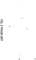
- FIG. 2 schematically illustrates the structure of another conventional electronic device.
- the voltage regulator module 12 is disposed on the second surface of the system board 13. That is, the voltage regulator module 12 is located at the position of the output capacitor 14 as shown in FIG. 1A .
- the voltage regulator module 12 and the central processing unit 11 are located at opposite sides of the system board 13.
- the layout of the inner components of the voltage regulator module 12 needs to be adjusted. For example, the installation position of the output capacitor is changed from the second surface of the system board 13 to the inner space of the voltage regulator module 12. Consequently, the volume of the electronic device 1' is effectively reduced.
- the output capacitor 14 is located near the output terminal of the voltage regulator module 12 and the input terminal of the central processing unit 11, the dynamic switching performance of the voltage regulator module 12 is enhanced.
- the first side of the voltage regulator module 12 is welded on the system board 13, and the second side of the voltage regulator module 12 is fixed on the casing of the electronic device 1' through a heat sink and spring screws.
- the heat from the voltage regulator module 12 cannot be effectively transferred to the casing of electronic device 1' and dissipated away through the casing of the electronic device 1'.
- the voltage regulator module 12 is unable to withstand the pressure from the heat sink and the spring screws.
- the output capacitor is disposed within the voltage regulator module.
- the voltage regulator module 12 includes a plurality of components for transferring signals. For example, a signal communication part composed of a plurality of pins is disposed within the voltage regulator module 12.
- the plurality of pins of the signal communication part are mounted on the printed circuit board of the voltage regulator module 12. Since the gap between every two pins of the signal communication part is large, the number of pins mounted on the given area is limited. That is, the distribution density of the pins is low. Moreover, since the cross-section area of each pin is small, the reliability of mounting the pin is usually unsatisfied. In case that the soldering materials between the pins are connected, a short-circuited problem occurs.
- a voltage regulator module includes a first circuit board assembly and a magnetic core assembly.
- the first circuit board assembly includes a first printed circuit board, a plurality of switch elements and a first molding compound layer.
- the plurality of switch elements are mounted on a first surface of the first printed circuit board.
- the first molding compound layer is formed on the first surface of the first printed circuit board to encapsulate the plurality of switch elements.
- the magnetic core assembly is arranged beside a second surface of the first printed circuit board, and includes a magnetic core portion and at least one first U-shaped copper structure.
- the magnetic core portion includes a plurality of openings. Each of the at least one first U-shaped copper structure is penetrated through two corresponding openings to define at least two inductors. A first terminal of each inductor and the corresponding switch element are connected in series to define a phase circuit.
- the present disclosure provides a voltage regulator module.
- the first U-shaped copper structures are penetrated through the magnetic core portion to define the inductors. Since the U-shaped copper structure has good supporting property and thermal conductivity, the capability of the voltage regulator module to withstand the pressure from the casing of the electronic device will be enhanced. Due to the good thermal conductivity of copper, the heat from the inductor can be transferred rapidly and effectively. Consequently, the thermal resistance in the thermal conduction path is decreased.
- the output capacitor is embedded within the second printed circuit board or encapsulated on the second printed circuit board. Consequently, the areas of the bonding pads on the second printed circuit board to weld the magnetic core assembly will be increased. Since the pressure applied to the ball grid arrays of the second printed circuit board is distributed more uniformly, the product reliability is enhanced and more output capacitors can be mounted on the second printed circuit board.
- a signal communication part includes a conduction circuit board with a plurality of conduction fingers and a plurality of surface pins. While the signal communication part is welded on the bonding pads of the first circuit board assembly or the second circuit board assembly, the lateral solder wicking efficacy is achieved and the soldering material is not spread to the adjacent pins. Since the soldering materials between the two surface pins are not connected, the short-circuited problem is avoided. Under this circumstance, the gap between the adjacent surface pins of the signal communication part is reduced, and the pins distribution density is increased. Consequently, the volume of the voltage regulator module is reduced, and power density of the voltage regulator module is enhanced.
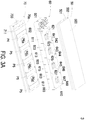
- FIG. 3A is a schematic exploded view illustrating a voltage regulator module according to a first embodiment of the present disclosure and taken along a viewpoint.
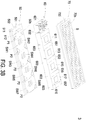
- FIG. 3B is a schematic exploded view illustrating the voltage regulator module of FIG. 3A and taken along another viewpoint.
- FIG. 4 is a schematic equivalent circuit diagram illustrating the voltage regulator module of FIG. 3A .
- the voltage regulator module 3 may be installed in an electronic device. In case that the central processing unit of the electronic device requires a large amount of current, the voltage regulator module 3 is a multi-phase buck converter. Consequently, the capability of the voltage regulator module 3 to output electricity is effectively enhanced.
- the voltage regulator module 3 includes a plurality of switch elements 30, a plurality of inductors L, at least one input capacitor Cin and at least one output capacitor Cout.
- the switch elements 30 are driver and metal-oxide-semiconductor field-effect transistors (also referred as a Dr.MOS element).
- each Dr.MOS element 30 and a first terminal SW of the corresponding inductor L are electrically connected with each other in series to define a phase buck circuit.
- the voltage regulator module 3 includes eight phase buck circuits, i.e., the first phase buck circuit to the eighth phase buck circuit from top to bottom.
- the voltage regulator module 3 includes eight Dr.MOS elements 30 and eight inductors L.
- the input side of the voltage regulator module 3 includes a positive input end Vin+ and a negative input end Vin-.
- the first terminals of the eight phase buck circuits are connected with each other in parallel and electrically connected with the input capacitor Cin.
- the output side of the voltage regulator module 3 includes a positive output terminal Vo+ and a negative output terminal Vo-.
- the negative input end Vin- and the negative output terminal Vo- are electrically connected with a common terminal.
- the second terminals of the eight phase buck circuits are connected with each other in parallel and electrically connected with the output capacitor Cout.
- a first terminal of the output capacitor Cout is electrically connected with the positive output terminal Vo+ of the voltage regulator module 3.
- a second terminal of the output capacitor Cout is electrically connected with the negative output terminal Vo- of the voltage regulator module 3.
- a first terminal of the input capacitor Cin is electrically connected with the positive input end Vin+ of the voltage regulator module 3.
- a second terminal of the input capacitor Cin is electrically connected with the negative input end Vin- of the voltage regulator module 3.
- each Dr.MOS element 30 includes a switch and a driver for driving the switch.
- the Dr.MOS element 30 has a heat dissipation surface for dissipating heat along a single side.
- the voltage regulator module 3 further includes a control circuit 40. After the control circuit 40 samples the output voltage of the voltage regulator module 3 and the output current of each phase buck circuit, the control circuit 40 generates four pulse width modulation signals PWM1, PWM2, PWM3 and PWM4. The phase difference between every two adjacent pulse width modulation signals is 90 degree. Every two adjacent phase buck circuits are controlled by the control circuit 40 according to one pulse width modulation signal.
- the first phase buck circuit and the second phase buck circuit are controlled according to the first pulse width modulation signal PWM1
- the third phase buck circuit and the fourth phase buck circuit are controlled according to the second pulse width modulation signal PWM2
- the fifth phase buck circuit and the sixth phase buck circuit are controlled according to the third pulse width modulation signal PWM3
- the seventh phase buck circuit and the eighth phase buck circuit are controlled according to the fourth pulse width modulation signal PWM4.
- the voltage regulator module 3 is a multi-layered structure with more than two layers. Consequently, the ability of the voltage regulator module 3 to withstand the pressure from the casing of the electronic device is increased, and the heat from the voltage regulator module 3 is effectively transferred to the casing or the heat sink of the electronic device.
- the voltage regulator module 3 is a three-layered structure comprising a first circuit board assembly 50, a magnetic core assembly 60 and a second circuit board assembly 70.
- the first circuit board assembly 50 includes a first printed circuit board 501 and a first molding compound layer 502.
- All Dr.MOS elements 30 and all input capacitors Cin are mounted on a first surface 50a of the first printed circuit board 501 by a welding process or through a conductive adhesive (see FIG. 3D ).
- the heat dissipation surfaces of the Dr.MOS elements 30 are in contact with the first surface 50a of the first printed circuit board 501.
- the first molding compound layer 502 is disposed on the first surface 50a of the first printed circuit board 501.
- the first surface 50a of the first printed circuit board 501, the Dr.MOS elements 30 and the input capacitors Cin are encapsulated by the first molding compound layer 502 through a plastic molding process.
- An external surface 503 of the first molding compound layer 502 is a flat surface.
- the external surface 503 is attached and fixed on a casing or a heat sink of the electronic device. Since the external surface 503 is a flat surface, the contact area between the external surface 503 and the casing (or the heat sink) is increased. The increased contact area is helpful to reduce the thermal resistance, increase the heat dissipating capability of the voltage regulator module 3, uniformly distribute the pressure from the casing and increase the pressure resistance of the first circuit board assembly 50.
- first bonding pads P1, four pairs of second bonding pads P2, an even number of third bonding pads, a plurality of perforations 511 and at least one blind hole 512 are disposed on a second surface 50b of the first printed circuit board 501.
- the first bonding pads P1 are electrically connected with the positive input end Vin+ of the voltage regulator module 3.
- the second bonding pads P2 are electrically connected with the negative output terminal Vo- of the voltage regulator module 3.
- the even number of third bonding pads include eight third bonding pads SW1, SW2, SW3, SW4, SW5, SW6, SW7 and SW8. Each third bonding pad is electrically connected with the first terminal SW of the corresponding inductor L.
- the perforations 511 run through the first printed circuit board 501.
- the blind hole 512 does not run through the first printed circuit board 501.
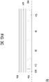
- FIG. 3C is a schematic cross-sectional view illustrating a variant example of a first circuit board assembly of the voltage regulator module according to the first embodiment of the present disclosure.
- each Dr.MOS element 30 has a first heat dissipation surface and a second heat dissipation surface, which are opposed to each other. Consequently, the heat can be dissipated along bilateral sides.
- the first heat dissipation surface is in contact with the first surface 50a of the first printed circuit board 501.
- the Dr.MOS elements 30 and the input capacitors Cin are encapsulated by the first molding compound layer 502, the external surface 503 of the first molding compound layer 502 is polished. Consequently, the second heat dissipation surfaces of the Dr.MOS elements 30 are exposed outside the external surface 503 of the first molding compound layer 502. Then, the Dr.MOS elements 30 are indirectly attached on the casing of the electronic device through a heat sink or directly attached on the casing of the electronic device. In such way, the thermal resistance is reduced, and the heat dissipating efficacy is enhanced.
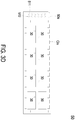
- FIG. 3D schematically illustrates the layout structure of the electronic components on the first surface of the first printed circuit board of the voltage regulator module according to the first embodiment of the present disclosure.
- the eight Dr.MOS elements 30 are divided into two rows.
- the four Dr.MOS elements 30 in the first row and the four Dr.MOS elements 30 in the second row are mounted on the first surface 50a of the first printed circuit board 501.
- the installation directions of the four Dr.MOS elements 30 in the first row are identical.
- the installation directions of the four Dr.MOS elements 30 in the second row are identical.
- the installation directions of the four Dr.MOS elements 30 in the first row and the installation directions of the four Dr.MOS elements 30 in the second row are opposite.
- the wires between the eight Dr.MOS elements 30 and the first terminals SW of the corresponding inductors L are shorter.
- the input capacitors Cin are uniformly distributed around the Dr.MOS elements 30.
- the magnetic core assembly 60 is arranged beside the first circuit board assembly 50.
- the magnetic core assembly 60 is located under the first circuit board assembly 50 and arranged beside the second surface 50b of the first printed circuit board 501.
- the magnetic core assembly 60 includes a magnetic core portion 610 and at least one first U-shaped copper structure. Each first U-shaped copper structure is penetrated through the magnetic core portion 610. Consequently, two inductors are defined by the magnetic core portion 610 and the two lateral posts of the first U-shaped copper structure.
- the voltage regulator module 3 includes eight phase buck circuits. That is, the voltage regulator module 3 includes eight inductors L. As shown in FIGS.
- the magnetic core assembly 60 includes four first U-shaped copper structures 621, 623, 625 and 627.
- the eight lateral posts of the four first U-shaped copper structures 621, 623, 625 and 627 are correlated to the eight windings of the eight inductors L.
- each first U-shaped copper structure is penetrated through the magnetic core portion 610 to define two inductors L. Consequently, the eight inductors L are defined by four first U-shaped copper structures. Under this circumstance, the number of the first U-shaped copper structures is decreased. Moreover, since the U-shaped copper structure has good supporting property and thermal conductivity, the U-shaped copper structure can be arranged between the first circuit board assembly 50 and the second circuit board assembly 70 to support the first circuit board assembly 50 and the second circuit board assembly 70. Consequently, the capability of the voltage regulator module 3 to withstand the pressure from the casing of the electronic device will be enhanced. Due to the good thermal conductivity of copper, the heat from the inductor L can be transferred rapidly and effectively. Consequently, the thermal resistance in the thermal conduction path is decreased. Due to low resistivity of copper, the conduction resistance of the inductor is decreased. Consequently, the conduction loss of the inductor is decreased, and the conversion efficiency of the voltage regulator module 3 is increased.
- the second circuit board assembly 70 includes a second printed circuit board 703 and at least one output capacitor Cout. Preferably but not exclusively, the at least one output capacitor Cout is embedded within the second printed circuit board 703.
- the second printed circuit board 703 includes a fourth bonding pad P4, four fifth bonding pads P5, four sixth bonding pads P6a, P6b, P6c, P6d, a plurality of blind holes 711 and a plurality of ball grid arrays (BGA) B.
- the fourth bonding pad P4, the four fifth bonding pads P5, the four sixth bonding pads P6a, P6b, P6c, P6d and the plurality of blind holes 711 are installed on/in a first surface 70a of the second printed circuit board 703.
- the first surface 70a of the second printed circuit board 703 is arranged beside the magnetic core assembly 60.
- the fourth bonding pad P4 is electrically connected with the positive input end Vin+ of the voltage regulator module 3.
- the four fifth bonding pads P5 are electrically connected with the negative output terminal Vo- of the voltage regulator module 3.
- the sixth bonding pads P6a, P6b, P6c and P6d are electrically connected with the positive output terminal Vo+ of the voltage regulator module 3.
- the plurality of ball grid arrays B are disposed on a second surface 70b of the second printed circuit board 703.
- the plurality of ball grid arrays B are electrically connected with the ball grid arrays of the central processing unit on the system board of the electronic device.
- the gaps and networks of the plurality of ball grid arrays B on the second surface 70b of the second printed circuit board 703 correspond to those of the ball grid arrays on the system board.
- the plurality of ball grid arrays B are electrically connected with the plurality of bonding pads on the first surface 70a of the second printed circuit board 703 through the internal traces of the second printed circuit board 703.
- the voltage regulator module 3 withstands the pressure from the electronic device because of screwing means or other reasons.
- the first surface 70a of the second printed circuit board 703 is exerted by the pressure uniformly
- the plurality of ball grid arrays B on the second surface 70b of the second printed circuit board 703 are exerted by the pressure uniformly.
- the ball grid arrays B are exerted by the pressure non-uniformly and some ball grid arrays B withstand the larger pressure, the soldering material is possibly cracked or detached and the product reliability is impaired.
- the areas of the bonding pads on the first surface 70a of the second printed circuit board 703 to weld the magnetic core assembly 60 need to be increased.
- the output capacitors Cout are embedded or encapsulated. The approach of embedding or encapsulating the output capacitors Cout will be described as follows.
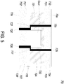
- FIG. 5 is a schematic cross-sectional view illustrating an example of embedding the output capacitor in the second printed circuit board according to the first embodiment of the present disclosure. For succinctness, only one output capacitor Cout embedded in the second printed circuit board 703 is shown in FIG. 5 .
- the second printed circuit board 703 includes a substrate 723, an interface layer 724, a plurality of first electroplating layers 731, 731', a plurality of second electroplating layers 732, 732', a plurality of first insulation layers 733, 733' and a plurality of second insulation layers 734, 734'.
- the substrate 723 includes a plurality of bonding pads 727.
- the output capacitor Cout is welded on the corresponding bonding pads 727. That is, the output capacitor Cout is fixed on the substrate 723 through the bonding pads 727.
- the interface layer 724 is made of AjinomotoBuild-up Film (ABF).
- the output capacitor Cout is mounted on a first surface of the substrate 723.
- the interface layer 724 is formed over the first surface of the substrate 723 and the output capacitor Cout. After the interface layer 724 is baked at a specified temperature (e.g., 180°C) for a specified time period (e.g., 30 minutes), the interface layer 724 is solidified into an insulation layer.
- the first electroplating layers 731 and 731' are copper layers that are laminated and electroplated on a top surface of the interface layer 724 and a second surface of the substrate 723, respectively.
- the thickness of the first electroplating layer 731 (and 731') is about 3OZ.
- two plated through holes are formed in the interface layer 724, and two plated through holes are formed in the substrate 723.
- the two plated through holes of the interface layer 724 and the two plated through holes of the substrate 723 are aligned with the two bonding pads 727, respectively.
- the two plated through holes of the interface layer 724 and the two plated through holes of the substrate 723 are connected with each other through the two bonding pads 727, which are connected with the output capacitor Cout.
- the first insulation layers 733 and 733' are formed on a top surface of the first electroplating layer 731 and a bottom surface of the first electroplating layer 731', respectively.
- the second electroplating layers 732 and 732' are copper layers that are laminated and electroplated on a top surface of the first insulation layer 733 and a bottom surface of the first insulation layer 733', respectively.
- the thickness of the second electroplating layer 732 (and 732') is about 3OZ.
- two plated through holes are formed in the first insulation layer 733, and two plated through holes are formed in the first insulation layer 733'.
- the two plated through holes of the first insulation layer 733 are aligned and contacted with the two plated through holes of the interface layer 724 so that the two plated through holes of the first insulation layer 733 are connected with the two bonding pads 727, which are connected with the output capacitor Cout.
- the two plated through holes of the first insulation layer 733' are aligned and contacted with the two plated through holes of the substrate 723 so that the two plated through holes of the first insulation layer 733' are connected with the two bonding pads 727, which are connected with the output capacitor Cout.
- the second insulation layers 734 and 734' are formed on a top surface of the second electroplating layer 732 and a bottom surface of the second electroplating layer 732', respectively.
- Two electroplating layers i.e. two cooper layers
- the thickness of the electroplating layer is about 3OZ.
- two plated through holes are formed in the second insulation layer 734, and two plated through holes are formed in the second insulation layer 734'.
- the two plated through holes of the second insulation layer 734 are aligned and contacted with the two plated through holes of the first insulation layer 733 so that the two plated through holes of the second insulation layer 734 are connected with the two plated through holes of the first insulation layer 733, the two plated through holes of the interface layer 724 and the two bonding pads 727, which are connected with the output capacitor Cout.
- the two plated through holes of the second insulation layer 734' are aligned and contacted with the two plated through holes of the first insulation layer 733' so that the two plated through holes of the second insulation layer 734' are connected with the two plated through holes of the first insulation layer 733', the two plated through holes of the substrate 723 and the two bonding pads 727, which are connected with the output capacitor Cout.
- one of the plated through holes of the second insulation layer 734, one of the plated through holes of the first insulation layer 733 and one of the plated through holes of the interface layer 724 are collaboratively defined as a first conducting line 725.
- one of the plated through holes of the second insulation layer 734', one of the plated through holes of the first insulation layer 733' and one of the plated through holes of the substrate 723 are collaboratively defined as a first conducting line 725'.
- the other one of the plated through holes of the second insulation layer 734, the other one of the plated through holes of the first insulation layer 733 and the other one of the plated through holes of the interface layer 724 are collaboratively defined as a second conducting line 726.
- the other one of the plated through holes of the second insulation layer 734', the other one of the plated through holes of the first insulation layer 733' and the other one of the plated through holes of the substrate 723 are collaboratively defined as a second conducting line 726'.
- the plated through holes of the above layers in the left side are collaboratively defined as a first conducting line.
- the plated through holes of the above layers in the right side are collaboratively defined as a second conducting line.
- the first conducting line 725, 725' is electrically connected with the first terminal of the output capacitor Cout, the positive output terminal Vo+ of the voltage regulator module 3 and the first surface 70a and the second surface 70b of the second printed circuit board 703.
- the second conducting line 726, 726' is connected with the second terminal of the output capacitor Cout, the negative output terminal Vo- of the voltage regulator module 3 and the first surface 70a and the second surface 70b of the second printed circuit board 703. Since the output capacitors Cout are embedded in the second printed circuit board 703, the voltage regulator module 3 can be equipped with more output capacitors. In addition, the output capacitors Cout are not interfered by other components of the second printed circuit board 703.
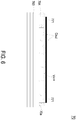
- FIG. 6 is a schematic cross-sectional view illustrating an example of encapsulating the output capacitor in the second printed circuit board according to the first embodiment of the present disclosure.
- the output capacitor Cout is encapsulated in the second printed circuit board 703.
- the output capacitor Cout is fixed on the first surface 70a of the second printed circuit board 703.
- the second circuit board assembly 70 further includes a plurality of copper blocks 771 and a second molding compound layer 704.
- the copper blocks 771 are fixed on the first surface 70a of the second printed circuit board 703 to provide a supporting function.
- the first surface 70a of the second printed circuit board 703, the output capacitor Cout and the plurality of copper blocks 771 are encapsulated by the second molding compound layer 704 through a plastic molding process.
- the copper blocks 771 are rectangular structures. Moreover, the top surfaces of the copper blocks 771 are exposed outside the top surface of the second molding compound layer 704 through natural exposure or a polishing process.
- the fourth bonding pad P4 is electroplated on the top surfaces of the second molding compound layer 704 and electrically connected with the corresponding copper blocks 771 exposed outside the second molding compound layer 704.
- the copper blocks 771 are higher than the output capacitor Cout. Consequently, after the plastic molding process, the top surfaces of the copper blocks 771 are exposed outside the top surface of the second molding compound layer 704 through natural exposure or the polishing process.
- the four fifth bonding pads P5 and the four sixth bonding pads P6a, P6b, P6c, P6d may be electroplated on the top surface of the second molding compound layer 704 and electrically connected with the exposed copper blocks.
- FIG. 7 is a schematic cross-sectional view illustrating a variant example of encapsulating the output capacitor in the second printed circuit board.
- each of the copper blocks 771 is a trapezoidal column structure with a bottom surface and a top surface. The area of the bottom surface is smaller than the area of the top surface.
- the bottom surfaces of the trapezoidal column structures are fixed on the first surface 70a of the second printed circuit board 703. Moreover, the top surfaces of the trapezoidal column structures are exposed outside the top surface of the second molding compound layer 704 through natural exposure or a polishing process.
- the fourth bonding pad P4 and the fifth bonding pads P5 (and/or the sixth bonding pads P6a, P6b, P6c, P6d) are formed on the exposed copper blocks 771.
- the area of the top surface of the trapezoid column structure is at least 1.3 times the area of the bottom surface of the trapezoid column structure.
- the output capacitor Cout is encapsulated in the second printed circuit board 703. Since the top side of the second circuit board assembly 70 is a flat plane, the larger-size bonding pad can be formed on the flat plane and the contact area between the second circuit board assembly 70 and the magnetic core assembly 60 is increased. Since the area of the second circuit board assembly 70 to receive the pressure is increased, the pressure applied to the ball grid arrays B on the second surface 70b of the second printed circuit board 703 is distributed more uniformly. Under this circumstance, the product reliability is enhanced.
- FIG. 8 is a schematic cross-sectional view illustrating the magnetic core portion of the magnetic core assembly of the voltage regulator module according to the first embodiment of the present disclosure.
- the magnetic core portion 610 includes four core units 611, 613, 615 and 617, which are connected with each other.
- each of the core units 611, 613, 615 and 617 is a square core with four rounded corners.
- each core unit is a circular core.
- Two parallel openings 811 are formed in a middle region of the core unit 611.
- Two parallel openings 813 are formed in a middle region of the core unit 613.
- Two parallel openings 815 are formed in a middle region of the core unit 615.
- Two parallel openings 817 are formed in a middle region of the core unit 617.
- the openings 811, 813, 815, 817 are square-shaped.
- the sizes and shapes of the openings 811, 813, 815 and 817 match the sizes and shapes of the lateral posts of the first U-shaped copper structures 621, 623, 625 and 627, respectively.
- the lateral posts of the first U-shaped copper structures 621, 623, 625 and 627 are respectively penetrated through the openings 811, 813, 815 and 817 to define eight inductors L.
- the two lateral posts of the first U-shaped copper structure 621 are penetrated through the openings 811, respectively.
- the inductor L of the first phase buck circuit and the inductor L of the second phase buck circuit are defined by the two lateral posts of the first U-shaped copper structure 621 and the core unit 611 collaboratively. The rest may be deduced by analogy.
- the first U-shaped copper structure 621 includes two top surfaces 641 and 642 and a bottom surface 651.
- the two top surfaces 641 and 642 are fixed on and electrically connected with the two third bonding pads SW1 and SW2 on the second surface 50b of the first printed circuit board 501.
- the bottom surface 651 is fixed on and electrically connected with the sixth bonding pad P6a of the second circuit board assembly 70.
- the first U-shaped copper structure 623 includes two top surfaces 643 and 644 and a bottom surface 653.
- the two top surfaces 643 and 644 are fixed on and electrically connected with the two third bonding pads SW3 and SW4 on the second surface 50b of the first printed circuit board 501.
- the bottom surface 653 is fixed on and electrically connected with the sixth bonding pad P6b of the second circuit board assembly 70.
- the first U-shaped copper structure 625 includes two top surfaces 645 and 646 and a bottom surface 655.
- the two top surfaces 645 and 646 are fixed on and electrically connected with the two third bonding pads SW5 and SW6 on the second surface 50b of the first printed circuit board 505.
- the bottom surface 655 is fixed on and electrically connected with the sixth bonding pad P6c of the second circuit board assembly 70.
- the first U-shaped copper structure 627 includes two top surfaces 647 and 648 and a bottom surface 657.
- the two top surfaces 647 and 648 are fixed on and electrically connected with the two third bonding pads SW7 and SW8 on the second surface 50b of the first printed circuit board 507.
- the bottom surface 657 is fixed on and electrically connected with the sixth bonding pad P6d of the second circuit board assembly 70.
- the magnetic field lines of every two adjacent core units 611, 613, 615, 617 are overlapped to create a first magnetic overlap region.
- first magnetic overlap regions 831, 832 and 833 indicated by oblique lines are shown in FIG. 8 .
- the magnetic field lines of every two inductors are overlapped to create a second magnetic overlap region.
- four second magnetic overlap regions 841, 842, 843 and 844 are shown in FIG. 8 .
- Each second magnetic overlap region is arranged between the two openings of the corresponding core unit.
- the DC magnetic fluxes are balanced out and the AC magnetic fluxes are superposed.
- the DC magnetic fluxes are balanced out and the AC magnetic fluxes are balanced out.
- the DC magnetic fluxes and the AC magnetic fluxes in the four second magnetic overlap regions 841, 842, 843 and 844 cannot be completely balanced out. That is, a small amount of DC magnetic flux and a small amount of AC magnetic flux are retained.
- each first magnetic overlap region e.g., 831, 832 or 833
- the area of each second magnetic overlap region is smaller than a half area of the area of the non-magnetic overlap region of each core unit (e.g., 801, 802, 803 or 804).
- Each of the core units 611, 613, 615 and 617 includes two air gaps.
- the core unit 611 includes the two air gaps 821 and 822, which are symmetrically arranged at two opposite sides of the openings 811.
- the core unit 613 includes the two air gaps 823 and 824, which are symmetrically arranged at two opposite sides of the openings 813.
- the core unit 615 includes the two air gaps 825 and 826, which are symmetrically arranged at two opposite sides of the openings 815.
- the core unit 617 includes the two air gaps 827 and 828, which are symmetrically arranged at two opposite sides of the openings 817. These air gaps can withstand the magnetic pressure averagely.
- the magnetic core portion 610 is an integral structure.
- the combination of the magnetic core portion 610 and the first U-shaped copper structures 621, 623, 625 and 627 is installed between the first circuit board assembly 50 and the second circuit board assembly 70.
- the magnetic core assembly 60 further includes a plurality of second U-shaped copper structures 603 and a third U-shaped copper structure 602.
- the two top surfaces of the third U-shaped copper structure 602 are welded on and electrically connected with the two first bonding pads P1 on the second surface 50b of the first printed circuit board 501.
- the bottom surface of the third U-shaped copper structure 602 is welded on and electrically connected with the fourth bonding pad P4 of the second circuit board assembly 70.
- the two top surfaces of each second U-shaped copper structure 603 are welded on and electrically connected with the corresponding two second bonding pads P2 on the second surface 50b of the first printed circuit board 501.
- the bottom surface of each second U-shaped copper structure 603 is welded on and electrically connected with the corresponding fifth bonding pad P5 of the second circuit board assembly 70.
- the heights of the first U-shaped copper structures 621, 623, 625, 627, the second U-shaped copper structures 603 and the third U-shaped copper structure 602 are equal or substantially the same. Moreover, the shapes of the inner surfaces of the third U-shaped copper structure 602 and the second U-shaped copper structures 603 match the shape of the magnetic core portion 610. The outer surfaces of the third U-shaped copper structure 602 and the second U-shaped copper structures 603 are flat. The first U-shaped copper structures 621, 623, 625, 627, the second U-shaped copper structure 603 and the third U-shaped copper structure 602 are supported between the first circuit board assembly 50 and the second circuit board assembly 70.
- the capability of the voltage regulator module 3 to withstand the pressure from the casing of the electronic device will be enhanced. Due to the good thermal conductivity of copper, the heat from the inductor L can be transferred to the second circuit board assembly 70 rapidly and effectively. Consequently, the thermal resistance in the thermal conduction path is decreased.
- the first U-shaped copper structures 621, 623, 625, 627, the second U-shaped copper structures 603 and the third U-shaped copper structure 602 can provide the good supporting capability. Consequently, the magnetic core portion 610 may be slightly shorter than the first U-shaped copper structures 621, 623, 625, 627, the second U-shaped copper structures 603 and the third U-shaped copper structure 602. In this design, the pressure to be withstood by the magnetic core portion 610 is reduced. Consequently, the possibility of causing the crack of the magnetic core portion 610 by the large pressure will be minimized.
- a process of assembling the magnetic core assembly 60 will be descried as follows. Firstly, the top surfaces of the first U-shaped copper structures 621, 623, 625, 627, the second U-shaped copper structures 603 and the third U-shaped copper structure 602 face upwardly. Then, the inner sides of the bottom surfaces of the first U-shaped copper structures 621, 623, 625, 627, the second U-shaped copper structures 603 and the third U-shaped copper structure 602 are dispensed with glue. Then, the first U-shaped copper structures 621, 623, 625, 627, the second U-shaped copper structures 603 and the third U-shaped copper structure 602 are locked on the magnetic core portion 610. Consequently, the magnetic core assembly 60 is assembled.
- the magnetic core assembly 60 is combined with the first circuit board assembly 50 and the second circuit board assembly 70 through a welding process. Consequently, the voltage regulator module 3 is produced and the production process is simplified.
- the shapes of the first U-shaped copper structures 621, 623, 625, 627, the second U-shaped copper structures 603 and the third U-shaped copper structure 602 are similar to that of the U-shaped magnetic cores of the conventional magnetic components. Therefore, the shapes of the U-shaped copper structures are not particularly shown in the drawings of the present disclosure.
- the voltage regulator module 3 further includes a signal communication part 601.
- the signal communication part 601 includes a plurality of pins. The plurality of pins are divided into a first pin group and a second pin group. The first terminals of the pins in the first pin group are fixed in the corresponding perforations 511 of the first printed circuit board 501 by welding. The first terminals of the pins in the second pin group are fixed in the blind holes 512 of the first printed circuit board 501 by welding. The second terminals of all pins are fixed in the corresponding blind holes 711 of the second printed circuit board 703 by welding.
- the signal communication part 601 is used for transferring the control signal between the first circuit board assembly 50 and the second circuit board assembly 70.
- the uses of the perforations 511 are helpful for fixing the signal communication part 601. Due to the blind holes 512, the first surface 50a of the first printed circuit board 501 is retained to mount the separate components (e.g., the input capacitors Cin). Consequently, the voltage regulator module 3 can meet the high-power density requirements. Similarly, due to the blind holes 711, the second surface 70b of the second printed circuit board 703 is retained to mount more ball grid arrays B and the inner space of the second printed circuit board 703 is retained to accommodate more separate components (e.g., the output capacitors Cout).
- FIG. 9A is a schematic exploded view illustrating a voltage regulator module according to a second embodiment of the present disclosure and taken along a viewpoint.
- FIG. 9B is a schematic exploded view illustrating the voltage regulator module of FIG. 9A and taken along another viewpoint.
- FIG. 10 is a planar view illustrating a signal communication part of the voltage regulator module as shown in FIG. 9A .
- Component parts and elements corresponding to those of the first embodiment are designated by identical numeral references, and detailed descriptions thereof are omitted.
- the signal communication part 661 does not includes the pins. Instead, the signal communication part 661 includes a conduction circuit board 662.
- a plurality of conduction pads 561 are formed on the second surface 50b of the first printed circuit board 501 to replace the perforations and the blind holes.
- a plurality of conduction pads 761 are formed on the second printed circuit board 703 to replace the perforations and the blind holes.
- the conduction circuit board 662 includes a plurality of conduction fingers 663 and a plurality of surface pins 664.
- the plurality of conduction fingers 663 are located at a first lateral side and a second lateral side of the conduction circuit board 662, which are opposed to each other. Every two conduction fingers 663 that are aligned with each other and located at two opposite sides belong to the same power network or different power networks.
- the conduction fingers 663 are gold-plated structures or tin-plated structures.
- the plurality of surface pins 664 are electroplated on the top side and the bottom side of the conduction circuit board 662. The top side and the bottom side of the conduction circuit board 662 are opposed to each other and arranged between the first lateral side and the second lateral side.
- the first ends of the conduction fingers 663 are contacted with the corresponding top-side surface pins 664.
- the second ends of the conduction fingers 663 are contacted with the corresponding bottom-side surface pins 664.
- the surface pins 664 contacted with the first specified conduction finger 663 and the surface pins 664 contacted with the second specified conduction finger 663 are not electrically connected with each other.
- the signal communication part 661 is arranged between the first circuit board assembly 50 and the second circuit board assembly 70 along a vertical direction.
- the signal communication part 661 is fixed on and electrically connected with the first circuit board assembly 50 through the conduction pads 561 and the corresponding surface pins 664.
- the signal communication part 661 is fixed on and electrically connected with the second circuit board assembly 70 through the conduction pads 761 and the corresponding surface pins 664.
- the signal communication part of the conventional voltage regulator module uses a plurality of fins to transfer signal, and thus some drawbacks occur.
- the signal communication part 661 of the voltage regulator module 3 of the present disclosure is specially designed. While the signal communication part 661 is welded on the bonding pads of the first circuit board assembly 50 or the second circuit board assembly 70, the lateral solder wicking efficacy is achieved and the soldering material is not spread to the adjacent pins. Since the soldering materials between the two surface pins 664 are not connected, the short-circuited problem is avoided. Under this circumstance, the gap between the adjacent surface pins 664 of the signal communication part 661 is reduced, and the pins distribution density is increased.
- the volume of the voltage regulator module 3 is reduced, and power density of the voltage regulator module 3 is enhanced.
- the conduction circuit board 662 of the signal communication part 661 is decreased, the size of the signal communication part 661 is reduced and the overall size of the voltage regulator module 3 is reduced. Consequently, more space can be provided to mount other separate components (e.g., the output capacitors Cout).
- the signal communication part 661 is electrically connected with the first circuit board assembly 50 or the second circuit board assembly 70 through a single-side wiring pattern or through the interconnect traces of the conduction circuit board.
- the signal communication part 661 is adhered on the magnetic core portion 610 or at least one of the first U-shaped copper structures 621, 623, 625, 627, the second U-shaped copper structures 603 and the third U-shaped copper structure 602 to define a signal communication module.
- the signal communication module 661 is directly installed between the first circuit board assembly 50 and the second circuit board assembly 70. Since the signal communication part 661 is adhered on the magnetic core portion 610 or at least one of the U-shaped copper structures, the perforations or blind holes can be omitted. In such way, the first circuit board assembly 50 and the second circuit board assembly 70 are not inclined during the welding process, the size of the voltage regulator module 3 is reduced, and production process is simplified.
- the conduction circuit board 662 of the signal communication part 661 is arranged vertically, the height of the conduction circuit board 662 can be adjusted more precisely. Under this circumstance, the smoothness of the contact surface between the magnetic core assembly 60 and the first circuit board assembly 50 (and the second circuit board assembly 70) will be enhanced.
- the plurality of ball grid arrays B are disposed on the second surface 70b of the second printed circuit board 703, and the first surface 70a of the second printed circuit board 703 (or the surface of the second printed circuit board 703 beside the magnetic core assembly 60) has to be welded and combined with the magnetic core assembly 60.
- the first surface of the printed circuit board is coated with soldering paste and then the component is placed on the soldering paste.
- the second surface of the printed circuit board is coated with soldering paste and the component is placed on the soldering paste. Then, a second reflow process is performed.
- the second reflow process is performed on the second surface of the printed circuit board, the solder point on the first surface is heated and possibly molten. Under this circumstance, the component is detached from the printed circuit board. Especially when the component is large and weighty, the problem is more serious.
- the temperature of the second reflow process is 5 degrees lower than the temperature of the first reflow process.
- the second surface 50b of the first printed circuit board 501 is an internal welding surface
- the first surface 70a of the second printed circuit board 703 (or the surface of the second printed circuit board 703 beside the magnetic core assembly 60) is also an internal welding surface.
- the second surface 70b of the second printed circuit board 703 has to be welded on the system board through the plurality of ball grid arrays B. Since the internal solder points of the voltage regulator module 3 are molten twice, the components are possibly shifted.
- the voltage regulator module 3 and the central processing unit are located at two opposite sides of the system board. After the voltage regulator module 3 is welded on the system board, the system board is turned over and then the central processing unit is welded on the system board.
- the ball grid arrays B, the solder points on the first surface 70a of the second printed circuit board 703 or the solder points on the second surface 50b of the first printed circuit board 501 are molten again because of the large weight of the voltage regulator module 3. Meanwhile, the internal components of the voltage regulator module 3 are possibly detached.
- the magnetic core assembly 60 is fixed on the first circuit board assembly 50 and/or the second circuit board assembly 70 through a conductive adhesive. After the conductive adhesive is heated and solidified, the conductive adhesive is not molten or deformed again. Consequently, the problems of detaching or shifting the components during the welding process will be avoided, and the reliability and convenience of assembling the voltage regulator module 3 will be enhanced. Moreover, since the soldering material is replaced by the conductive adhesive, the number of the reflow processes is largely reduced and the product reliability is increased.
- the voltage regulator module is equipped with the first circuit board assembly 50 and the magnetic core assembly 60 and not equipped with the second circuit board assembly 70.
- the output capacitor Cout is mounted on the system board of the electronic device, and the bottom surfaces of the U-shaped copper structures of the magnetic core assembly 60 are directly welded on the corresponding bonding pads of the system board or fixed on the system board through the conductive adhesive.
- the second circuit board assembly 70 in the first embodiment or the second embodiment is replaced by the system board.
Landscapes
- Engineering & Computer Science (AREA)
- Power Engineering (AREA)
- Microelectronics & Electronic Packaging (AREA)
- Physics & Mathematics (AREA)
- General Physics & Mathematics (AREA)
- Theoretical Computer Science (AREA)
- Manufacturing & Machinery (AREA)
- Thermal Sciences (AREA)
- Human Computer Interaction (AREA)
- General Engineering & Computer Science (AREA)
- Computer Hardware Design (AREA)
- Electromagnetism (AREA)
- Radar, Positioning & Navigation (AREA)
- Automation & Control Theory (AREA)
- Dc-Dc Converters (AREA)
- Combinations Of Printed Boards (AREA)
Abstract
A voltage regulator module (3) includes a first circuit board assembly (50) and a magnetic core assembly (60). The first circuit board assembly (50) includes a first printed circuit board (501), a plurality of switch elements (30) and a first molding compound layer (502). The switch elements (30) are mounted on a first surface (50a) of the first printed circuit board (501). The first molding compound layer (502) is formed on the first surface (50a) of the first printed circuit board (501) to encapsulate the switch elements (30). The magnetic core assembly (60) is arranged beside a second surface (50b) of the first printed circuit board (501), and includes a magnetic core portion (610) and at least one first U-shaped copper structure (621, 623, 625, 627). The magnetic core portion (610) includes a plurality of openings (811, 813, 815, 817). Each first U-shaped copper structure (621, 623, 625, 627) is penetrated through two corresponding openings (811, 813, 815, 817) to define two inductors (L). A first terminal (SW) of each inductor (L) and the corresponding switch element (30) are connected in series to define a phase circuit.
Description
- The present disclosure relates to a voltage regulator module, and more particularly to a voltage regulator module capable of reducing loss, increasing heat dissipation efficiency, withstanding increased pressure, disposing more output capacitors therein and/or decreasing the volume thereof.
- Please refer to
FIGS. 1A and1B .FIG. 1A schematically illustrates the structure of a conventional electronic device.FIG. 1B schematically illustrates the structure of a voltage regulator module of the electronic device as shown inFIG. 1A . As shown inFIGS. 1A and1B , theelectronic device 1 includes a central processing unit (CPU) 11, avoltage regulator module 12 and asystem board 13. Thevoltage regulator module 12 is used for converting an input voltage into a regulated voltage and providing the regulated voltage to thecentral processing unit 11. Thevoltage regulator module 12 and thecentral processing unit 11 are disposed on a first surface of thesystem board 13. For meeting the load dynamic switching requirements, the output terminal of thevoltage regulator module 12 is located near the input terminal of thecentral processing unit 11. - Moreover, the
voltage regulator module 12 further includes anoutput capacitor 14, aprinted circuit board 15 and amagnetic element 16. Theoutput capacitor 14 is disposed on a second surface of thesystem board 13. The first surface and the second surface of thesystem board 13 are opposed to each other. Theoutput capacitor 14 is located beside the input terminal of thecentral processing unit 11. Themagnetic element 16 is disposed on the printedcircuit board 15. Moreover, a switch element is disposed in a vacant space between the printedcircuit board 15 and themagnetic element 16. The printedcircuit board 15 is disposed on the first surface of thesystem board 13. The heat from thevoltage regulator module 12 can be transferred to thesystem board 13 through the printedcircuit board 15. Moreover, the heat is dissipated away through a heat dissipation mechanism (not shown) of thesystem board 13. - Recently, the required current for the
central processing unit 11 is gradually increased. In addition, the trend of the volume of the electronic device is toward miniaturization. Since thecentral processing unit 11 and thevoltage regulator module 12 are located at the same side of thesystem board 13, the electronic device cannot meet the load dynamic switching requirements. - For reducing the volume of the electronic device and effectively enhancing the dynamic switching performance of the voltage regulator module, another electronic device is disclosed.
FIG. 2 schematically illustrates the structure of another conventional electronic device. In the electronic device 1' ofFIG. 2 , thevoltage regulator module 12 is disposed on the second surface of thesystem board 13. That is, thevoltage regulator module 12 is located at the position of theoutput capacitor 14 as shown inFIG. 1A . Under this circumstance, thevoltage regulator module 12 and thecentral processing unit 11 are located at opposite sides of thesystem board 13. Correspondingly, the layout of the inner components of thevoltage regulator module 12 needs to be adjusted. For example, the installation position of the output capacitor is changed from the second surface of thesystem board 13 to the inner space of thevoltage regulator module 12. Consequently, the volume of the electronic device 1' is effectively reduced. Moreover, theoutput capacitor 14 is located near the output terminal of thevoltage regulator module 12 and the input terminal of thecentral processing unit 11, the dynamic switching performance of thevoltage regulator module 12 is enhanced. - Although the dynamic switching performance of the
voltage regulator module 12 of the electronic device 1' as shown inFIG. 2 is enhanced, there are still some drawbacks. For example, the first side of thevoltage regulator module 12 is welded on thesystem board 13, and the second side of thevoltage regulator module 12 is fixed on the casing of the electronic device 1' through a heat sink and spring screws. Firstly, the heat from thevoltage regulator module 12 cannot be effectively transferred to the casing of electronic device 1' and dissipated away through the casing of the electronic device 1'. Secondly, thevoltage regulator module 12 is unable to withstand the pressure from the heat sink and the spring screws. As mentioned above, the output capacitor is disposed within the voltage regulator module. Thirdly, a plurality of ball grid arrays are usually mounted on the printed circuit board of thevoltage regulator module 12. In case that the force applied to the ball grid arrays is not uniform, the soldering material is possibly cracked or detached and the product reliability is impaired. For solving this problem, the surface of the printed circuit board of thevoltage regulator module 12 has to provide a large space for improving the force on the ball grid arrays. However, the installation space of the output capacitor is restricted. That is, thevoltage regulator module 12 cannot be equipped with more output capacitors according to the practical requirements. Fourthly, thevoltage regulator module 12 includes a plurality of components for transferring signals. For example, a signal communication part composed of a plurality of pins is disposed within thevoltage regulator module 12. The plurality of pins of the signal communication part are mounted on the printed circuit board of thevoltage regulator module 12. Since the gap between every two pins of the signal communication part is large, the number of pins mounted on the given area is limited. That is, the distribution density of the pins is low. Moreover, since the cross-section area of each pin is small, the reliability of mounting the pin is usually unsatisfied. In case that the soldering materials between the pins are connected, a short-circuited problem occurs. - Therefore, there is a need of providing an improved voltage regulator module in order to overcome the drawbacks of the conventional technologies.
- In accordance with an aspect of the present disclosure, a voltage regulator module is provided. The voltage regulator module includes a first circuit board assembly and a magnetic core assembly. The first circuit board assembly includes a first printed circuit board, a plurality of switch elements and a first molding compound layer. The plurality of switch elements are mounted on a first surface of the first printed circuit board. The first molding compound layer is formed on the first surface of the first printed circuit board to encapsulate the plurality of switch elements. The magnetic core assembly is arranged beside a second surface of the first printed circuit board, and includes a magnetic core portion and at least one first U-shaped copper structure. The magnetic core portion includes a plurality of openings. Each of the at least one first U-shaped copper structure is penetrated through two corresponding openings to define at least two inductors. A first terminal of each inductor and the corresponding switch element are connected in series to define a phase circuit.
- From the above descriptions, the present disclosure provides a voltage regulator module. The first U-shaped copper structures are penetrated through the magnetic core portion to define the inductors. Since the U-shaped copper structure has good supporting property and thermal conductivity, the capability of the voltage regulator module to withstand the pressure from the casing of the electronic device will be enhanced. Due to the good thermal conductivity of copper, the heat from the inductor can be transferred rapidly and effectively. Consequently, the thermal resistance in the thermal conduction path is decreased.
- Moreover, the output capacitor is embedded within the second printed circuit board or encapsulated on the second printed circuit board. Consequently, the areas of the bonding pads on the second printed circuit board to weld the magnetic core assembly will be increased. Since the pressure applied to the ball grid arrays of the second printed circuit board is distributed more uniformly, the product reliability is enhanced and more output capacitors can be mounted on the second printed circuit board.
- Moreover, a signal communication part includes a conduction circuit board with a plurality of conduction fingers and a plurality of surface pins. While the signal communication part is welded on the bonding pads of the first circuit board assembly or the second circuit board assembly, the lateral solder wicking efficacy is achieved and the soldering material is not spread to the adjacent pins. Since the soldering materials between the two surface pins are not connected, the short-circuited problem is avoided. Under this circumstance, the gap between the adjacent surface pins of the signal communication part is reduced, and the pins distribution density is increased. Consequently, the volume of the voltage regulator module is reduced, and power density of the voltage regulator module is enhanced.
- The above contents of the present disclosure will become more readily apparent to those ordinarily skilled in the art after reviewing the following detailed description and accompanying drawings, in which:
-
-
FIG. 1A schematically illustrates the structure of a conventional electronic device; -
FIG. 1B schematically illustrates the structure of a voltage regulator module of the electronic device as shown inFIG. 1A ; -
FIG. 2 schematically illustrates the structure of another conventional electronic device; -
FIG. 3A is a schematic exploded view illustrating a voltage regulator module according to a first embodiment of the present disclosure and taken along a viewpoint; -
FIG. 3B is a schematic exploded view illustrating the voltage regulator module ofFIG. 3A and taken along another viewpoint; -
FIG. 3C is a schematic cross-sectional view illustrating a variant example of a first circuit board assembly of the voltage regulator module according to the first embodiment of the present disclosure; -
FIG. 3D schematically illustrates the layout structure of the electronic components on the first surface of the first printed circuit board of the voltage regulator module according to the first embodiment of the present disclosure; -
FIG. 4 is a schematic equivalent circuit diagram illustrating the voltage regulator module ofFIG. 3A ; -
FIG. 5 is a schematic cross-sectional view illustrating an example of installing the output capacitor in the second printed circuit board according to the first embodiment of the present disclosure; -
FIG. 6 is a schematic cross-sectional view illustrating an example of encapsulating the output capacitor in the second printed circuit board according to the first embodiment of the present disclosure; -
FIG. 7 is a schematic cross-sectional view illustrating a variant example of encapsulating the output capacitor in the second printed circuit board; -
FIG. 8 is a schematic cross-sectional view illustrating the magnetic core portion of the magnetic core assembly of the voltage regulator module according to the first embodiment of the present disclosure; -
FIG. 9A is a schematic exploded view illustrating a voltage regulator module according to a second embodiment of the present disclosure and taken along a viewpoint; -
FIG. 9B is a schematic exploded view illustrating the voltage regulator module ofFIG. 9A and taken along another viewpoint; and -
FIG. 10 is a planar view illustrating a signal communication part of the voltage regulator module as shown inFIG. 9A . - The present disclosure will now be described more specifically with reference to the following embodiments. It is to be noted that the following descriptions of preferred embodiments of this disclosure are presented herein for purpose of illustration and description only. It is not intended to be exhaustive or to be limited to the precise form disclosed.
- Please refer to
FIGS. 3A ,3B and4 .FIG. 3A is a schematic exploded view illustrating a voltage regulator module according to a first embodiment of the present disclosure and taken along a viewpoint.FIG. 3B is a schematic exploded view illustrating the voltage regulator module ofFIG. 3A and taken along another viewpoint.FIG. 4 is a schematic equivalent circuit diagram illustrating the voltage regulator module ofFIG. 3A . Thevoltage regulator module 3 may be installed in an electronic device. In case that the central processing unit of the electronic device requires a large amount of current, thevoltage regulator module 3 is a multi-phase buck converter. Consequently, the capability of thevoltage regulator module 3 to output electricity is effectively enhanced. Thevoltage regulator module 3 includes a plurality ofswitch elements 30, a plurality of inductors L, at least one input capacitor Cin and at least one output capacitor Cout. For example, theswitch elements 30 are driver and metal-oxide-semiconductor field-effect transistors (also referred as a Dr.MOS element). - As shown in
FIG. 4 , eachDr.MOS element 30 and a first terminal SW of the corresponding inductor L are electrically connected with each other in series to define a phase buck circuit. In this embodiment, thevoltage regulator module 3 includes eight phase buck circuits, i.e., the first phase buck circuit to the eighth phase buck circuit from top to bottom. In other words, thevoltage regulator module 3 includes eightDr.MOS elements 30 and eight inductors L. The input side of thevoltage regulator module 3 includes a positive input end Vin+ and a negative input end Vin-. The first terminals of the eight phase buck circuits are connected with each other in parallel and electrically connected with the input capacitor Cin. The output side of thevoltage regulator module 3 includes a positive output terminal Vo+ and a negative output terminal Vo-. The negative input end Vin- and the negative output terminal Vo- are electrically connected with a common terminal. The second terminals of the eight phase buck circuits are connected with each other in parallel and electrically connected with the output capacitor Cout. A first terminal of the output capacitor Cout is electrically connected with the positive output terminal Vo+ of thevoltage regulator module 3. A second terminal of the output capacitor Cout is electrically connected with the negative output terminal Vo- of thevoltage regulator module 3. A first terminal of the input capacitor Cin is electrically connected with the positive input end Vin+ of thevoltage regulator module 3. A second terminal of the input capacitor Cin is electrically connected with the negative input end Vin- of thevoltage regulator module 3. - In an embodiment, each
Dr.MOS element 30 includes a switch and a driver for driving the switch. TheDr.MOS element 30 has a heat dissipation surface for dissipating heat along a single side. Moreover, thevoltage regulator module 3 further includes acontrol circuit 40. After thecontrol circuit 40 samples the output voltage of thevoltage regulator module 3 and the output current of each phase buck circuit, thecontrol circuit 40 generates four pulse width modulation signals PWM1, PWM2, PWM3 and PWM4. The phase difference between every two adjacent pulse width modulation signals is 90 degree. Every two adjacent phase buck circuits are controlled by thecontrol circuit 40 according to one pulse width modulation signal. For example, the first phase buck circuit and the second phase buck circuit are controlled according to the first pulse width modulation signal PWM1, the third phase buck circuit and the fourth phase buck circuit are controlled according to the second pulse width modulation signal PWM2, the fifth phase buck circuit and the sixth phase buck circuit are controlled according to the third pulse width modulation signal PWM3, and the seventh phase buck circuit and the eighth phase buck circuit are controlled according to the fourth pulse width modulation signal PWM4. - In accordance with a feature of the present disclosure, the
voltage regulator module 3 is a multi-layered structure with more than two layers. Consequently, the ability of thevoltage regulator module 3 to withstand the pressure from the casing of the electronic device is increased, and the heat from thevoltage regulator module 3 is effectively transferred to the casing or the heat sink of the electronic device. In the embodiment as shown inFIGS. 3A and3B , thevoltage regulator module 3 is a three-layered structure comprising a firstcircuit board assembly 50, amagnetic core assembly 60 and a secondcircuit board assembly 70. The firstcircuit board assembly 50 includes a first printedcircuit board 501 and a firstmolding compound layer 502. AllDr.MOS elements 30 and all input capacitors Cin are mounted on afirst surface 50a of the first printedcircuit board 501 by a welding process or through a conductive adhesive (seeFIG. 3D ). The heat dissipation surfaces of theDr.MOS elements 30 are in contact with thefirst surface 50a of the first printedcircuit board 501. The firstmolding compound layer 502 is disposed on thefirst surface 50a of the first printedcircuit board 501. Thefirst surface 50a of the first printedcircuit board 501, theDr.MOS elements 30 and the input capacitors Cin are encapsulated by the firstmolding compound layer 502 through a plastic molding process. Anexternal surface 503 of the firstmolding compound layer 502 is a flat surface. Theexternal surface 503 is attached and fixed on a casing or a heat sink of the electronic device. Since theexternal surface 503 is a flat surface, the contact area between theexternal surface 503 and the casing (or the heat sink) is increased. The increased contact area is helpful to reduce the thermal resistance, increase the heat dissipating capability of thevoltage regulator module 3, uniformly distribute the pressure from the casing and increase the pressure resistance of the firstcircuit board assembly 50. - As shown in
FIG. 3B , two first bonding pads P1, four pairs of second bonding pads P2, an even number of third bonding pads, a plurality ofperforations 511 and at least oneblind hole 512 are disposed on asecond surface 50b of the first printedcircuit board 501. The first bonding pads P1 are electrically connected with the positive input end Vin+ of thevoltage regulator module 3. The second bonding pads P2 are electrically connected with the negative output terminal Vo- of thevoltage regulator module 3. In this embodiment, the even number of third bonding pads include eight third bonding pads SW1, SW2, SW3, SW4, SW5, SW6, SW7 and SW8. Each third bonding pad is electrically connected with the first terminal SW of the corresponding inductor L. Theperforations 511 run through the first printedcircuit board 501. Theblind hole 512 does not run through the first printedcircuit board 501. - It is noted that numerous modifications and alterations may be made while retaining the teachings of the disclosure.
FIG. 3C is a schematic cross-sectional view illustrating a variant example of a first circuit board assembly of the voltage regulator module according to the first embodiment of the present disclosure. In this embodiment, eachDr.MOS element 30 has a first heat dissipation surface and a second heat dissipation surface, which are opposed to each other. Consequently, the heat can be dissipated along bilateral sides. The first heat dissipation surface is in contact with thefirst surface 50a of the first printedcircuit board 501. After thefirst surface 50a of the first printedcircuit board 501, theDr.MOS elements 30 and the input capacitors Cin are encapsulated by the firstmolding compound layer 502, theexternal surface 503 of the firstmolding compound layer 502 is polished. Consequently, the second heat dissipation surfaces of theDr.MOS elements 30 are exposed outside theexternal surface 503 of the firstmolding compound layer 502. Then, theDr.MOS elements 30 are indirectly attached on the casing of the electronic device through a heat sink or directly attached on the casing of the electronic device. In such way, the thermal resistance is reduced, and the heat dissipating efficacy is enhanced. -
FIG. 3D schematically illustrates the layout structure of the electronic components on the first surface of the first printed circuit board of the voltage regulator module according to the first embodiment of the present disclosure. As shown inFIG. 3D , the eightDr.MOS elements 30 are divided into two rows. The fourDr.MOS elements 30 in the first row and the fourDr.MOS elements 30 in the second row are mounted on thefirst surface 50a of the first printedcircuit board 501. The installation directions of the fourDr.MOS elements 30 in the first row are identical. The installation directions of the fourDr.MOS elements 30 in the second row are identical. Moreover, the installation directions of the fourDr.MOS elements 30 in the first row and the installation directions of the fourDr.MOS elements 30 in the second row are opposite. In this design, the wires between the eightDr.MOS elements 30 and the first terminals SW of the corresponding inductors L are shorter. The input capacitors Cin are uniformly distributed around theDr.MOS elements 30. - Please refer to
FIGS. 3A and3B again. Themagnetic core assembly 60 is arranged beside the firstcircuit board assembly 50. In this embodiment, themagnetic core assembly 60 is located under the firstcircuit board assembly 50 and arranged beside thesecond surface 50b of the first printedcircuit board 501. Themagnetic core assembly 60 includes amagnetic core portion 610 and at least one first U-shaped copper structure. Each first U-shaped copper structure is penetrated through themagnetic core portion 610. Consequently, two inductors are defined by themagnetic core portion 610 and the two lateral posts of the first U-shaped copper structure. In this embodiment, thevoltage regulator module 3 includes eight phase buck circuits. That is, thevoltage regulator module 3 includes eight inductors L. As shown inFIGS. 3A and3B , themagnetic core assembly 60 includes four firstU-shaped copper structures U-shaped copper structures - As mentioned above, each first U-shaped copper structure is penetrated through the
magnetic core portion 610 to define two inductors L. Consequently, the eight inductors L are defined by four first U-shaped copper structures. Under this circumstance, the number of the first U-shaped copper structures is decreased. Moreover, since the U-shaped copper structure has good supporting property and thermal conductivity, the U-shaped copper structure can be arranged between the firstcircuit board assembly 50 and the secondcircuit board assembly 70 to support the firstcircuit board assembly 50 and the secondcircuit board assembly 70. Consequently, the capability of thevoltage regulator module 3 to withstand the pressure from the casing of the electronic device will be enhanced. Due to the good thermal conductivity of copper, the heat from the inductor L can be transferred rapidly and effectively. Consequently, the thermal resistance in the thermal conduction path is decreased. Due to low resistivity of copper, the conduction resistance of the inductor is decreased. Consequently, the conduction loss of the inductor is decreased, and the conversion efficiency of thevoltage regulator module 3 is increased. - Please refer to
FIGS. 3A ,3B and4 again. The secondcircuit board assembly 70 includes a second printedcircuit board 703 and at least one output capacitor Cout. Preferably but not exclusively, the at least one output capacitor Cout is embedded within the second printedcircuit board 703. The second printedcircuit board 703 includes a fourth bonding pad P4, four fifth bonding pads P5, four sixth bonding pads P6a, P6b, P6c, P6d, a plurality ofblind holes 711 and a plurality of ball grid arrays (BGA) B. The fourth bonding pad P4, the four fifth bonding pads P5, the four sixth bonding pads P6a, P6b, P6c, P6d and the plurality ofblind holes 711 are installed on/in afirst surface 70a of the second printedcircuit board 703. Thefirst surface 70a of the second printedcircuit board 703 is arranged beside themagnetic core assembly 60. The fourth bonding pad P4 is electrically connected with the positive input end Vin+ of thevoltage regulator module 3. The four fifth bonding pads P5 are electrically connected with the negative output terminal Vo- of thevoltage regulator module 3. The sixth bonding pads P6a, P6b, P6c and P6d are electrically connected with the positive output terminal Vo+ of thevoltage regulator module 3. The plurality of ball grid arrays B are disposed on asecond surface 70b of the second printedcircuit board 703. The plurality of ball grid arrays B are electrically connected with the ball grid arrays of the central processing unit on the system board of the electronic device. Preferably, the gaps and networks of the plurality of ball grid arrays B on thesecond surface 70b of the second printedcircuit board 703 correspond to those of the ball grid arrays on the system board. The plurality of ball grid arrays B are electrically connected with the plurality of bonding pads on thefirst surface 70a of the second printedcircuit board 703 through the internal traces of the second printedcircuit board 703. - Generally, the
voltage regulator module 3 withstands the pressure from the electronic device because of screwing means or other reasons. In case that thefirst surface 70a of the second printedcircuit board 703 is exerted by the pressure uniformly, the plurality of ball grid arrays B on thesecond surface 70b of the second printedcircuit board 703 are exerted by the pressure uniformly. Whereas, in case that the ball grid arrays B are exerted by the pressure non-uniformly and some ball grid arrays B withstand the larger pressure, the soldering material is possibly cracked or detached and the product reliability is impaired. For solving this problem, the areas of the bonding pads on thefirst surface 70a of the second printedcircuit board 703 to weld themagnetic core assembly 60 need to be increased. However, as the areas of the bonding pads are increased, the layout area for placing the output capacitors Cout is decreased. In accordance with the present disclosure, the output capacitors Cout are embedded or encapsulated. The approach of embedding or encapsulating the output capacitors Cout will be described as follows. -
FIG. 5 is a schematic cross-sectional view illustrating an example of embedding the output capacitor in the second printed circuit board according to the first embodiment of the present disclosure. For succinctness, only one output capacitor Cout embedded in the second printedcircuit board 703 is shown inFIG. 5 . The second printedcircuit board 703 includes asubstrate 723, aninterface layer 724, a plurality of first electroplating layers 731, 731', a plurality of second electroplating layers 732, 732', a plurality of first insulation layers 733, 733' and a plurality of second insulation layers 734, 734'. - The
substrate 723 includes a plurality ofbonding pads 727. The output capacitor Cout is welded on thecorresponding bonding pads 727. That is, the output capacitor Cout is fixed on thesubstrate 723 through thebonding pads 727. For example, theinterface layer 724 is made of AjinomotoBuild-up Film (ABF). The output capacitor Cout is mounted on a first surface of thesubstrate 723. Theinterface layer 724 is formed over the first surface of thesubstrate 723 and the output capacitor Cout. After theinterface layer 724 is baked at a specified temperature (e.g., 180°C) for a specified time period (e.g., 30 minutes), theinterface layer 724 is solidified into an insulation layer. - The first electroplating layers 731 and 731' are copper layers that are laminated and electroplated on a top surface of the
interface layer 724 and a second surface of thesubstrate 723, respectively. The thickness of the first electroplating layer 731 (and 731') is about 3OZ. Moreover, two plated through holes are formed in theinterface layer 724, and two plated through holes are formed in thesubstrate 723. The two plated through holes of theinterface layer 724 and the two plated through holes of thesubstrate 723 are aligned with the twobonding pads 727, respectively. Moreover, the two plated through holes of theinterface layer 724 and the two plated through holes of thesubstrate 723 are connected with each other through the twobonding pads 727, which are connected with the output capacitor Cout. - The first insulation layers 733 and 733' are formed on a top surface of the
first electroplating layer 731 and a bottom surface of the first electroplating layer 731', respectively. - The second electroplating layers 732 and 732' are copper layers that are laminated and electroplated on a top surface of the
first insulation layer 733 and a bottom surface of the first insulation layer 733', respectively. The thickness of the second electroplating layer 732 (and 732') is about 3OZ. Moreover, two plated through holes are formed in thefirst insulation layer 733, and two plated through holes are formed in the first insulation layer 733'. The two plated through holes of thefirst insulation layer 733 are aligned and contacted with the two plated through holes of theinterface layer 724 so that the two plated through holes of thefirst insulation layer 733 are connected with the twobonding pads 727, which are connected with the output capacitor Cout. The two plated through holes of the first insulation layer 733' are aligned and contacted with the two plated through holes of thesubstrate 723 so that the two plated through holes of the first insulation layer 733' are connected with the twobonding pads 727, which are connected with the output capacitor Cout. - The second insulation layers 734 and 734' are formed on a top surface of the
second electroplating layer 732 and a bottom surface of the second electroplating layer 732', respectively. Two electroplating layers (i.e. two cooper layers) are laminated and electroplated on a top surface of thesecond insulation layer 734 and a bottom surface of the second insulation layer 734', respectively, so as to form afirst surface 70a and asecond surface 70b of the second printedcircuit board 703. The thickness of the electroplating layer is about 3OZ. Moreover, two plated through holes are formed in thesecond insulation layer 734, and two plated through holes are formed in the second insulation layer 734'. The two plated through holes of thesecond insulation layer 734 are aligned and contacted with the two plated through holes of thefirst insulation layer 733 so that the two plated through holes of thesecond insulation layer 734 are connected with the two plated through holes of thefirst insulation layer 733, the two plated through holes of theinterface layer 724 and the twobonding pads 727, which are connected with the output capacitor Cout. The two plated through holes of the second insulation layer 734' are aligned and contacted with the two plated through holes of the first insulation layer 733' so that the two plated through holes of the second insulation layer 734' are connected with the two plated through holes of the first insulation layer 733', the two plated through holes of thesubstrate 723 and the twobonding pads 727, which are connected with the output capacitor Cout. - In the upper half and left side of the second printed
circuit board assembly 70, one of the plated through holes of thesecond insulation layer 734, one of the plated through holes of thefirst insulation layer 733 and one of the plated through holes of theinterface layer 724 are collaboratively defined as afirst conducting line 725. In the lower half and left side of the second printedcircuit board assembly 70, one of the plated through holes of the second insulation layer 734', one of the plated through holes of the first insulation layer 733' and one of the plated through holes of thesubstrate 723 are collaboratively defined as a first conducting line 725'. In the upper half and right side of the second printedcircuit board assembly 70, the other one of the plated through holes of thesecond insulation layer 734, the other one of the plated through holes of thefirst insulation layer 733 and the other one of the plated through holes of theinterface layer 724 are collaboratively defined as asecond conducting line 726. In the lower half and right side of the second printedcircuit board assembly 70, the other one of the plated through holes of the second insulation layer 734', the other one of the plated through holes of the first insulation layer 733' and the other one of the plated through holes of thesubstrate 723 are collaboratively defined as a second conducting line 726'. Namely, the plated through holes of the above layers in the left side are collaboratively defined as a first conducting line. The plated through holes of the above layers in the right side are collaboratively defined as a second conducting line. Thefirst conducting line 725, 725' is electrically connected with the first terminal of the output capacitor Cout, the positive output terminal Vo+ of thevoltage regulator module 3 and thefirst surface 70a and thesecond surface 70b of the second printedcircuit board 703. Thesecond conducting line 726, 726' is connected with the second terminal of the output capacitor Cout, the negative output terminal Vo- of thevoltage regulator module 3 and thefirst surface 70a and thesecond surface 70b of the second printedcircuit board 703. Since the output capacitors Cout are embedded in the second printedcircuit board 703, thevoltage regulator module 3 can be equipped with more output capacitors. In addition, the output capacitors Cout are not interfered by other components of the second printedcircuit board 703. -
FIG. 6 is a schematic cross-sectional view illustrating an example of encapsulating the output capacitor in the second printed circuit board according to the first embodiment of the present disclosure. In this embodiment, the output capacitor Cout is encapsulated in the second printedcircuit board 703. As shown inFIG. 6 , the output capacitor Cout is fixed on thefirst surface 70a of the second printedcircuit board 703. The secondcircuit board assembly 70 further includes a plurality of copper blocks 771 and a secondmolding compound layer 704. The copper blocks 771 are fixed on thefirst surface 70a of the second printedcircuit board 703 to provide a supporting function. Thefirst surface 70a of the second printedcircuit board 703, the output capacitor Cout and the plurality of copper blocks 771 are encapsulated by the secondmolding compound layer 704 through a plastic molding process. - In an embodiment, the copper blocks 771 are rectangular structures. Moreover, the top surfaces of the copper blocks 771 are exposed outside the top surface of the second
molding compound layer 704 through natural exposure or a polishing process. The fourth bonding pad P4 is electroplated on the top surfaces of the secondmolding compound layer 704 and electrically connected with the corresponding copper blocks 771 exposed outside the secondmolding compound layer 704. The copper blocks 771 are higher than the output capacitor Cout. Consequently, after the plastic molding process, the top surfaces of the copper blocks 771 are exposed outside the top surface of the secondmolding compound layer 704 through natural exposure or the polishing process. Similarly, the four fifth bonding pads P5 and the four sixth bonding pads P6a, P6b, P6c, P6d may be electroplated on the top surface of the secondmolding compound layer 704 and electrically connected with the exposed copper blocks. -
FIG. 7 is a schematic cross-sectional view illustrating a variant example of encapsulating the output capacitor in the second printed circuit board. In this embodiment, each of the copper blocks 771 is a trapezoidal column structure with a bottom surface and a top surface. The area of the bottom surface is smaller than the area of the top surface. The bottom surfaces of the trapezoidal column structures are fixed on thefirst surface 70a of the second printedcircuit board 703. Moreover, the top surfaces of the trapezoidal column structures are exposed outside the top surface of the secondmolding compound layer 704 through natural exposure or a polishing process. The fourth bonding pad P4 and the fifth bonding pads P5 (and/or the sixth bonding pads P6a, P6b, P6c, P6d) are formed on the exposed copper blocks 771. - Preferably, the area of the top surface of the trapezoid column structure is at least 1.3 times the area of the bottom surface of the trapezoid column structure. In the embodiment of
FIG. 6 orFIG. 7 , the output capacitor Cout is encapsulated in the second printedcircuit board 703. Since the top side of the secondcircuit board assembly 70 is a flat plane, the larger-size bonding pad can be formed on the flat plane and the contact area between the secondcircuit board assembly 70 and themagnetic core assembly 60 is increased. Since the area of the secondcircuit board assembly 70 to receive the pressure is increased, the pressure applied to the ball grid arrays B on thesecond surface 70b of the second printedcircuit board 703 is distributed more uniformly. Under this circumstance, the product reliability is enhanced. - Please refer to
FIGS. 3A ,3B and8. FIG. 8 is a schematic cross-sectional view illustrating the magnetic core portion of the magnetic core assembly of the voltage regulator module according to the first embodiment of the present disclosure. Themagnetic core portion 610 includes fourcore units core units parallel openings 811 are formed in a middle region of thecore unit 611. Twoparallel openings 813 are formed in a middle region of thecore unit 613. Twoparallel openings 815 are formed in a middle region of thecore unit 615. Twoparallel openings 817 are formed in a middle region of thecore unit 617. Preferably but not exclusively, theopenings openings U-shaped copper structures U-shaped copper structures openings U-shaped copper structure 621 are penetrated through theopenings 811, respectively. Consequently, the inductor L of the first phase buck circuit and the inductor L of the second phase buck circuit are defined by the two lateral posts of the firstU-shaped copper structure 621 and thecore unit 611 collaboratively. The rest may be deduced by analogy. - The first
U-shaped copper structure 621 includes twotop surfaces bottom surface 651. The twotop surfaces second surface 50b of the first printedcircuit board 501. Thebottom surface 651 is fixed on and electrically connected with the sixth bonding pad P6a of the secondcircuit board assembly 70. The firstU-shaped copper structure 623 includes twotop surfaces bottom surface 653. The twotop surfaces second surface 50b of the first printedcircuit board 501. Thebottom surface 653 is fixed on and electrically connected with the sixth bonding pad P6b of the secondcircuit board assembly 70. The firstU-shaped copper structure 625 includes twotop surfaces bottom surface 655. The twotop surfaces second surface 50b of the first printed circuit board 505. Thebottom surface 655 is fixed on and electrically connected with the sixth bonding pad P6c of the secondcircuit board assembly 70. The firstU-shaped copper structure 627 includes twotop surfaces bottom surface 657. The twotop surfaces second surface 50b of the first printed circuit board 507. Thebottom surface 657 is fixed on and electrically connected with the sixth bonding pad P6d of the secondcircuit board assembly 70. - In the
magnetic core portion 610, the magnetic field lines of every twoadjacent core units magnetic overlap regions FIG. 8 . In eachcore unit magnetic overlap regions FIG. 8 . Each second magnetic overlap region is arranged between the two openings of the corresponding core unit. In the three firstmagnetic overlap regions magnetic overlap regions magnetic overlap regions FIG. 8 are presented herein for purpose of illustration and description only. - Each of the
core units core unit 611 includes the twoair gaps openings 811. Thecore unit 613 includes the twoair gaps openings 813. Thecore unit 615 includes the twoair gaps openings 815. Thecore unit 617 includes the twoair gaps openings 817. These air gaps can withstand the magnetic pressure averagely. Preferably, themagnetic core portion 610 is an integral structure. Moreover, the combination of themagnetic core portion 610 and the firstU-shaped copper structures circuit board assembly 50 and the secondcircuit board assembly 70. - Please refer to
FIGS. 3A and3B . Themagnetic core assembly 60 further includes a plurality of secondU-shaped copper structures 603 and a thirdU-shaped copper structure 602. The two top surfaces of the thirdU-shaped copper structure 602 are welded on and electrically connected with the two first bonding pads P1 on thesecond surface 50b of the first printedcircuit board 501. The bottom surface of the thirdU-shaped copper structure 602 is welded on and electrically connected with the fourth bonding pad P4 of the secondcircuit board assembly 70. The two top surfaces of each secondU-shaped copper structure 603 are welded on and electrically connected with the corresponding two second bonding pads P2 on thesecond surface 50b of the first printedcircuit board 501. The bottom surface of each secondU-shaped copper structure 603 is welded on and electrically connected with the corresponding fifth bonding pad P5 of the secondcircuit board assembly 70. - The heights of the first
U-shaped copper structures U-shaped copper structures 603 and the thirdU-shaped copper structure 602 are equal or substantially the same. Moreover, the shapes of the inner surfaces of the thirdU-shaped copper structure 602 and the secondU-shaped copper structures 603 match the shape of themagnetic core portion 610. The outer surfaces of the thirdU-shaped copper structure 602 and the secondU-shaped copper structures 603 are flat. The firstU-shaped copper structures U-shaped copper structure 603 and the thirdU-shaped copper structure 602 are supported between the firstcircuit board assembly 50 and the secondcircuit board assembly 70. Consequently, the capability of thevoltage regulator module 3 to withstand the pressure from the casing of the electronic device will be enhanced. Due to the good thermal conductivity of copper, the heat from the inductor L can be transferred to the secondcircuit board assembly 70 rapidly and effectively. Consequently, the thermal resistance in the thermal conduction path is decreased. - The first
U-shaped copper structures U-shaped copper structures 603 and the thirdU-shaped copper structure 602 can provide the good supporting capability. Consequently, themagnetic core portion 610 may be slightly shorter than the firstU-shaped copper structures U-shaped copper structures 603 and the thirdU-shaped copper structure 602. In this design, the pressure to be withstood by themagnetic core portion 610 is reduced. Consequently, the possibility of causing the crack of themagnetic core portion 610 by the large pressure will be minimized. - A process of assembling the
magnetic core assembly 60 will be descried as follows. Firstly, the top surfaces of the firstU-shaped copper structures U-shaped copper structures 603 and the thirdU-shaped copper structure 602 face upwardly. Then, the inner sides of the bottom surfaces of the firstU-shaped copper structures U-shaped copper structures 603 and the thirdU-shaped copper structure 602 are dispensed with glue. Then, the firstU-shaped copper structures U-shaped copper structures 603 and the thirdU-shaped copper structure 602 are locked on themagnetic core portion 610. Consequently, themagnetic core assembly 60 is assembled. Then, themagnetic core assembly 60 is combined with the firstcircuit board assembly 50 and the secondcircuit board assembly 70 through a welding process. Consequently, thevoltage regulator module 3 is produced and the production process is simplified. In this embodiment, the shapes of the firstU-shaped copper structures U-shaped copper structures 603 and the thirdU-shaped copper structure 602 are similar to that of the U-shaped magnetic cores of the conventional magnetic components. Therefore, the shapes of the U-shaped copper structures are not particularly shown in the drawings of the present disclosure. - Please refer to
FIGS. 3A and3B again. Thevoltage regulator module 3 further includes asignal communication part 601. Thesignal communication part 601 includes a plurality of pins. The plurality of pins are divided into a first pin group and a second pin group. The first terminals of the pins in the first pin group are fixed in the correspondingperforations 511 of the first printedcircuit board 501 by welding. The first terminals of the pins in the second pin group are fixed in theblind holes 512 of the first printedcircuit board 501 by welding. The second terminals of all pins are fixed in the correspondingblind holes 711 of the second printedcircuit board 703 by welding. Thesignal communication part 601 is used for transferring the control signal between the firstcircuit board assembly 50 and the secondcircuit board assembly 70. - The uses of the
perforations 511 are helpful for fixing thesignal communication part 601. Due to theblind holes 512, thefirst surface 50a of the first printedcircuit board 501 is retained to mount the separate components (e.g., the input capacitors Cin). Consequently, thevoltage regulator module 3 can meet the high-power density requirements. Similarly, due to theblind holes 711, thesecond surface 70b of the second printedcircuit board 703 is retained to mount more ball grid arrays B and the inner space of the second printedcircuit board 703 is retained to accommodate more separate components (e.g., the output capacitors Cout). - Please refer to
FIGS. 9A ,9B and10 .FIG. 9A is a schematic exploded view illustrating a voltage regulator module according to a second embodiment of the present disclosure and taken along a viewpoint.FIG. 9B is a schematic exploded view illustrating the voltage regulator module ofFIG. 9A and taken along another viewpoint.FIG. 10 is a planar view illustrating a signal communication part of the voltage regulator module as shown inFIG. 9A . Component parts and elements corresponding to those of the first embodiment are designated by identical numeral references, and detailed descriptions thereof are omitted. In comparison with the first embodiment, thesignal communication part 661 does not includes the pins. Instead, thesignal communication part 661 includes aconduction circuit board 662. In this embodiment, a plurality ofconduction pads 561 are formed on thesecond surface 50b of the first printedcircuit board 501 to replace the perforations and the blind holes. Similarly, a plurality ofconduction pads 761 are formed on the second printedcircuit board 703 to replace the perforations and the blind holes. - The
conduction circuit board 662 includes a plurality ofconduction fingers 663 and a plurality of surface pins 664. The plurality ofconduction fingers 663 are located at a first lateral side and a second lateral side of theconduction circuit board 662, which are opposed to each other. Every twoconduction fingers 663 that are aligned with each other and located at two opposite sides belong to the same power network or different power networks. For example, theconduction fingers 663 are gold-plated structures or tin-plated structures. The plurality of surface pins 664 are electroplated on the top side and the bottom side of theconduction circuit board 662. The top side and the bottom side of theconduction circuit board 662 are opposed to each other and arranged between the first lateral side and the second lateral side. The first ends of theconduction fingers 663 are contacted with the corresponding top-side surface pins 664. The second ends of theconduction fingers 663 are contacted with the corresponding bottom-side surface pins 664. In case that a first specifiedconduction finger 663 and a second specifiedconduction finger 663 located at the two opposite sides belong to different power networks, the surface pins 664 contacted with the first specifiedconduction finger 663 and the surface pins 664 contacted with the second specifiedconduction finger 663 are not electrically connected with each other. - The
signal communication part 661 is arranged between the firstcircuit board assembly 50 and the secondcircuit board assembly 70 along a vertical direction. Thesignal communication part 661 is fixed on and electrically connected with the firstcircuit board assembly 50 through theconduction pads 561 and the corresponding surface pins 664. Thesignal communication part 661 is fixed on and electrically connected with the secondcircuit board assembly 70 through theconduction pads 761 and the corresponding surface pins 664. - As previously described, the signal communication part of the conventional voltage regulator module uses a plurality of fins to transfer signal, and thus some drawbacks occur. The
signal communication part 661 of thevoltage regulator module 3 of the present disclosure is specially designed. While thesignal communication part 661 is welded on the bonding pads of the firstcircuit board assembly 50 or the secondcircuit board assembly 70, the lateral solder wicking efficacy is achieved and the soldering material is not spread to the adjacent pins. Since the soldering materials between the twosurface pins 664 are not connected, the short-circuited problem is avoided. Under this circumstance, the gap between the adjacent surface pins 664 of thesignal communication part 661 is reduced, and the pins distribution density is increased. Consequently, the volume of thevoltage regulator module 3 is reduced, and power density of thevoltage regulator module 3 is enhanced. Moreover, since theconduction circuit board 662 of thesignal communication part 661 is decreased, the size of thesignal communication part 661 is reduced and the overall size of thevoltage regulator module 3 is reduced. Consequently, more space can be provided to mount other separate components (e.g., the output capacitors Cout). It is noted that numerous modifications and alterations may be made while retaining the teachings of the disclosure. For example, in another embodiment, thesignal communication part 661 is electrically connected with the firstcircuit board assembly 50 or the secondcircuit board assembly 70 through a single-side wiring pattern or through the interconnect traces of the conduction circuit board. - In another embodiment, the
signal communication part 661 is adhered on themagnetic core portion 610 or at least one of the firstU-shaped copper structures U-shaped copper structures 603 and the thirdU-shaped copper structure 602 to define a signal communication module. Thesignal communication module 661 is directly installed between the firstcircuit board assembly 50 and the secondcircuit board assembly 70. Since thesignal communication part 661 is adhered on themagnetic core portion 610 or at least one of the U-shaped copper structures, the perforations or blind holes can be omitted. In such way, the firstcircuit board assembly 50 and the secondcircuit board assembly 70 are not inclined during the welding process, the size of thevoltage regulator module 3 is reduced, and production process is simplified. Moreover, since theconduction circuit board 662 of thesignal communication part 661 is arranged vertically, the height of theconduction circuit board 662 can be adjusted more precisely. Under this circumstance, the smoothness of the contact surface between themagnetic core assembly 60 and the first circuit board assembly 50 (and the second circuit board assembly 70) will be enhanced. - As mentioned above, the plurality of ball grid arrays B are disposed on the
second surface 70b of the second printedcircuit board 703, and thefirst surface 70a of the second printed circuit board 703 (or the surface of the second printedcircuit board 703 beside the magnetic core assembly 60) has to be welded and combined with themagnetic core assembly 60. In accordance with the conventional double-side reflow process, the first surface of the printed circuit board is coated with soldering paste and then the component is placed on the soldering paste. After a first reflow process is completed, the second surface of the printed circuit board is coated with soldering paste and the component is placed on the soldering paste. Then, a second reflow process is performed. However, when the second reflow process is performed on the second surface of the printed circuit board, the solder point on the first surface is heated and possibly molten. Under this circumstance, the component is detached from the printed circuit board. Especially when the component is large and weighty, the problem is more serious. For solving this problem, the temperature of the second reflow process is 5 degrees lower than the temperature of the first reflow process. - In accordance with the present disclosure, the
second surface 50b of the first printedcircuit board 501 is an internal welding surface, and thefirst surface 70a of the second printed circuit board 703 (or the surface of the second printedcircuit board 703 beside the magnetic core assembly 60) is also an internal welding surface. After thevoltage regulator module 3 is assembled, thesecond surface 70b of the second printedcircuit board 703 has to be welded on the system board through the plurality of ball grid arrays B. Since the internal solder points of thevoltage regulator module 3 are molten twice, the components are possibly shifted. Thevoltage regulator module 3 and the central processing unit are located at two opposite sides of the system board. After thevoltage regulator module 3 is welded on the system board, the system board is turned over and then the central processing unit is welded on the system board. During the process of welding the central processing unit, the ball grid arrays B, the solder points on thefirst surface 70a of the second printedcircuit board 703 or the solder points on thesecond surface 50b of the first printedcircuit board 501 are molten again because of the large weight of thevoltage regulator module 3. Meanwhile, the internal components of thevoltage regulator module 3 are possibly detached. - For overcoming the above drawbacks, the
magnetic core assembly 60 is fixed on the firstcircuit board assembly 50 and/or the secondcircuit board assembly 70 through a conductive adhesive. After the conductive adhesive is heated and solidified, the conductive adhesive is not molten or deformed again. Consequently, the problems of detaching or shifting the components during the welding process will be avoided, and the reliability and convenience of assembling thevoltage regulator module 3 will be enhanced. Moreover, since the soldering material is replaced by the conductive adhesive, the number of the reflow processes is largely reduced and the product reliability is increased. - It is noted that numerous modifications and alterations may be made while retaining the teachings of the disclosure. For example, in another embodiment, the voltage regulator module is equipped with the first
circuit board assembly 50 and themagnetic core assembly 60 and not equipped with the secondcircuit board assembly 70. Under this circumstance, the output capacitor Cout is mounted on the system board of the electronic device, and the bottom surfaces of the U-shaped copper structures of themagnetic core assembly 60 are directly welded on the corresponding bonding pads of the system board or fixed on the system board through the conductive adhesive. In other words, the secondcircuit board assembly 70 in the first embodiment or the second embodiment is replaced by the system board.
Claims (15)
- A voltage regulator module (3), characterized in that the voltage regulator module (3) comprises:a first circuit board assembly (50) comprising a first printed circuit board (501), a plurality of switch elements (30) and a first molding compound layer (502), wherein the plurality of switch elements (30) are disposed on a first surface (50a) of the first printed circuit board (501), and the first molding compound layer (502) is formed on the first surface (50a) of the first printed circuit board (501) to encapsulate the plurality of switch elements (30); anda magnetic core assembly (60) arranged beside a second surface (50b) of the first printed circuit board (501), and comprising a magnetic core portion (610) and at least one first U-shaped copper structure (621, 623, 625, 627), wherein the magnetic core portion (610) comprises a plurality of openings (811, 813, 815, 817), and each of the at least one first U-shaped copper structure (621, 623, 625, 627) is penetrated through two corresponding openings (811, 813, 815, 817) to define at least two inductors (L), wherein a first terminal (SW) of each inductor (L) and the corresponding switch element (30) are connected in series to define a phase circuit.
- The voltage regulator module (3) according to claim 1, further comprising a second circuit board assembly (70), wherein the second circuit board assembly (70) is arranged beside the magnetic core assembly (60), and the magnetic core assembly (60) is arranged between the first circuit board assembly (50) and the second circuit board assembly (70), wherein the second circuit board assembly (70) comprises a second printed circuit board (703) and at least one output capacitor (Cout), a first surface (70a) and a second surface (70b) of the second printed circuit board (703) are opposed to each other, and the first surface (70a) of the second printed circuit board (703) is arranged beside the magnetic core assembly (60).
- The voltage regulator module (3) according to claim 2, wherein the second circuit board assembly (70) is a system board.
- The voltage regulator module (3) according to claim 2, wherein the magnetic core assembly (60) further comprises at least one second U-shaped copper structure (603) and a third U-shaped copper structure (602), wherein a height of the magnetic core portion (610) is lower than a height of the first U-shaped copper structure (621, 623, 625, 627), a height of the second U-shaped copper structure (603) and a height of the third U-shaped copper structure (602).
- The voltage regulator module (3) according to claim 4, wherein two first bonding pads (P1) and at least one pair of second bonding pads (P2) are disposed on the second surface (50b) of the first printed circuit board (501), and the second circuit board assembly (70) further comprises a fourth bonding pad (P4) and at least one fifth bonding pad (P5), wherein the first bonding pads (P1) and the fourth bonding pad (P4) are electrically connected with a positive input end (Vin+) of the voltage regulator module (3), the second bonding pads (P2) and the at least one fifth bonding pad (P5) are electrically connected with a negative output terminal (Vo-) of the voltage regulator module (3), the third U-shaped copper structure (602) is fixed on and electrically connected with the two first bonding pads (P1) and the fourth bonding pad (P4), each second U-shaped copper structure (603) is fixed on and electrically connected with the corresponding pair of second bonding pads (P2) and the corresponding fifth bonding pad (P5), and the first circuit board assembly (50) and the second circuit board assembly (70) are supported by the at least one first U-shaped copper structure (621, 623, 625, 627), the at least one second U-shaped copper structure (603) and the third U-shaped copper structure (602).
- The voltage regulator module (3) according to claim 2, wherein an even number of third bonding pads (SW1, SW2, SW3, SW4, SW5, SW6, SW7, SW8) are disposed on the second surface (50b) of the first printed circuit board (501), and the second circuit board assembly (70) further comprises at least one sixth bonding pad (P6a, P6b, P6c, P6d), wherein each third bonding pad (SW1, SW2, SW3, SW4, SW5, SW6, SW7, SW8) is electrically connected with the first terminal (SW) of the corresponding inductor L, the at least one sixth bonding pad (P6a, P6b, P6c, P6d) is electrically connected with a positive output terminal (Vo+) of the voltage regulator module (3), and each first U-shaped copper structure (621, 623, 625, 627) is fixed on and electrically connected with the corresponding two third bonding pads (SW1, SW2, SW3, SW4, SW5, SW6, SW7, SW8) and the corresponding sixth bonding pad (P6a, P6b, P6c, P6d), wherein each first U-shaped copper structure (621, 623, 625, 627) comprises two top surfaces (641, 642, 643, 644, 645, 646, 647, 648) and a bottom surface (651, 653, 655, 657), wherein the two top surfaces (641, 642, 643, 644, 645, 646, 647, 648) of the first U-shaped copper structure (621, 623, 625, 627) are fixed on and electrically connected with the corresponding two third bonding pads (SW1, SW2, SW3, SW4, SW5, SW6, SW7, SW8), and the bottom surface (651, 653, 655, 657) of the first U-shaped copper structure (621, 623, 625, 627) is fixed on and electrically connected with the corresponding sixth bonding pad (P6a, P6b, P6c, P6d).
- The voltage regulator module (3) according to claim 2, wherein the at least one output capacitor (Cout) is embedded within the second printed circuit board (703), or the at least one output capacitor (Cout) is mounted on the first surface (70a) of the second printed circuit board (703) through a plastic molding process, and wherein a plurality of ball grid arrays (B) are disposed on the second surface (70b) of the second printed circuit board (703).
- The voltage regulator module (3) according to claim 7, wherein the second circuit board assembly (70) further comprises a plurality of copper blocks (771) and a second molding compound layer (704), wherein the plurality of copper blocks (771) are fixed on the first surface (70a) of the second printed circuit board (703) to provide a supporting function, and the first surface (70a) of the second printed circuit board (703), the at least one output capacitor (Cout) and the plurality of copper blocks (771) are encapsulated by the second molding compound layer (704) through a plastic molding process, wherein a top surface of each copper block (771) is exposed outside the second molding compound layer (704), wherein each of the copper blocks (771) has a rectangular structure.
- The voltage regulator module (3) according to claim 7, wherein the second circuit board assembly (70) further comprises a plurality of copper blocks (771) and a second molding compound layer (704), wherein the plurality of copper blocks (771) are fixed on the first surface (70a) of the second printed circuit board (703) to provide a supporting function, and the first surface (70a) of the second printed circuit board (703), the at least one output capacitor (Cout) and the plurality of copper blocks (771) are encapsulated by the second molding compound layer (704) through a plastic molding process, wherein a top surface of each copper block (771) is exposed outside the second molding compound layer (704), wherein each of the copper blocks (771) has a trapezoid column structure with a bottom surface and a top surface, wherein the bottom surface and the top surface are parallel with each other, and an area of the bottom surface is smaller than an area of the top surface, wherein the bottom surface of the trapezoid column structure is fixed on the first surface (70a) of the second printed circuit board (703), the top surface of the trapezoid column structure is exposed outside the second molding compound layer (704), and a bonding pad (P4, P5, P6a, P6b, P6c, P6d) is electroplated on the top surface of the trapezoid column structure, wherein the area of the top surface of the trapezoid column structure is at least 1.3 times the area of the bottom surface of the trapezoid column structure.
- The voltage regulator module (3) according to claim 2, wherein a plurality of perforations (511) and a plurality of first blind holes (512) are formed in the second surface (50b) of the first printed circuit board (501), and a plurality of second blind holes (711) are formed in the first surface (70a) of the second printed circuit board (703), wherein the voltage regulator module (3) further comprises a signal communication part (601) with a plurality of pins, and the plurality of pins are divided into a first pin group and a second pin group, wherein first terminals of the pins in the first pin group are fixed in the corresponding perforations (511) of the first printed circuit board (501), first terminals of the pins in the second pin group are fixed in the first blind holes (512) of the first printed circuit board (501), second terminals of the plurality of pins are fixed in the corresponding second blind holes (711) of the second printed circuit board (703), and a control signal is transmitted between the first circuit board assembly (50) and the second circuit board assembly (70) through the signal communication part (601).
- The voltage regulator module (3) according to claim 2, wherein a plurality of first conduction pads (561) are formed on the second surface (50b) of the first printed circuit board (501), a plurality of second conduction pads (761) are formed on the second printed circuit board (703), the voltage regulator module (3) comprise a signal communication part (661) with a conduction circuit board (662), and the conduction circuit board (662) comprises a plurality of conduction fingers (663) and a plurality of surface pins (664), wherein the plurality of conduction fingers (663) are formed on at least one lateral side of the conduction circuit board (662), the plurality of surface pins (664) are electroplated on a top side and a bottom side of the conduction circuit board (662), a first end of each conduction finger (663) is contacted with the corresponding surface pin (664) on the top side, and a second end of each conduction finger (663) is contacted with the corresponding surface pin (664) on the bottom side, wherein the signal communication part (661) is arranged between the first circuit board assembly (50) and the second circuit board assembly (60) along a vertical direction, the signal communication part (661) is fixed on and electrically connected with the first circuit board assembly (50) through the first conduction pads (561) of the first printed circuit board (501) and the corresponding surface pins (664), the signal communication part (661) is fixed on and electrically connected with the second circuit board assembly (70) through the second conduction pads (761) of the second printed circuit board (703) and the corresponding surface pins (664), and a control signal is transmitted between the first circuit board assembly (50) and the second circuit board assembly (70) through the signal communication part (661).
- The voltage regulator module (3) according to claim 1, wherein the magnetic core assembly (60) is fixed on the first circuit board assembly (50) through a conductive adhesive.
- The voltage regulator module (3) according to claim 2, wherein the magnetic core assembly (60) is fixed between the first circuit board assembly (50) and the second circuit board assembly (70) through a conductive adhesive.
- The voltage regulator module (3) according to claim 1, further comprising an input capacitor (Cin), wherein the input capacitor (Cin) is disposed on the first surface (50a) of the first printed circuit board (501) and encapsulated by the first molding compound layer (502), wherein a first terminal of the input capacitor (Cin) is electrically connected with a positive input end (Vin+) of the voltage regulator module (3), and a second terminal of the input capacitor (Cin) is electrically connected with a negative input end (Vin-) of the voltage regulator module (3).
- The voltage regulator module (3) according to claim 1, wherein an external surface (503) of the first molding compound layer (502) is a flat surface, wherein each of the plurality of switch elements (30) is a driver and metal-oxide-semiconductor field-effect transistor, and the driver and metal-oxide-semiconductor field-effect transistor comprises a first heat dissipation surface and a second heat dissipation surface, wherein the first heat dissipation surface and the second heat dissipation surface are opposed to each other, the first heat dissipation surface is in contact with the first surface (50a) of the first printed circuit board (501), and the second heat dissipation surface is exposed outside the external surface (503) of the first molding compound layer (502).
Applications Claiming Priority (4)
| Application Number | Priority Date | Filing Date | Title |
|---|---|---|---|
| US201862743251P | 2018-10-09 | 2018-10-09 | |
| US201862770432P | 2018-11-21 | 2018-11-21 | |
| CN201811519354 | 2018-12-12 | ||
| CN201910900102.1A CN111313655B (en) | 2018-12-12 | 2019-09-23 | Voltage Regulation Module |
Publications (1)
| Publication Number | Publication Date |
|---|---|
| EP3637444A1 true EP3637444A1 (en) | 2020-04-15 |
Family
ID=68136249
Family Applications (1)
| Application Number | Title | Priority Date | Filing Date |
|---|---|---|---|
| EP19201084.1A Withdrawn EP3637444A1 (en) | 2018-10-09 | 2019-10-02 | Voltage regulator module |
Country Status (2)
| Country | Link |
|---|---|
| US (10) | US11488764B2 (en) |
| EP (1) | EP3637444A1 (en) |
Families Citing this family (32)
| Publication number | Priority date | Publication date | Assignee | Title |
|---|---|---|---|---|
| CN108809079B (en) * | 2017-05-05 | 2019-11-05 | 台达电子企业管理(上海)有限公司 | Power inverter, inductance element and inductance cut off control method |
| US11488764B2 (en) * | 2018-10-09 | 2022-11-01 | Delta Electronics, Inc. | Voltage regulator module |
| CN111415813B (en) | 2019-01-07 | 2022-06-17 | 台达电子企业管理(上海)有限公司 | Preparation method of inductor with vertical winding and injection mold thereof |
| US11901113B2 (en) | 2019-01-07 | 2024-02-13 | Delta Electronics (Shanghai) Co., Ltd. | Inversely coupled inductor and power supply module |
| CN114783727A (en) * | 2019-06-04 | 2022-07-22 | 台达电子工业股份有限公司 | Magnetic assembly |
| US11071206B2 (en) * | 2019-10-17 | 2021-07-20 | Infineon Technologies Austria Ag | Electronic system and processor substrate having an embedded power device module |
| US11147165B2 (en) | 2019-10-17 | 2021-10-12 | Infineon Technologies Austria Ag | Electronic system and interposer having an embedded power device module |
| US11183934B2 (en) | 2019-10-17 | 2021-11-23 | Infineon Technologies Americas Corp. | Embedded substrate voltage regulators |
| US20210118601A1 (en) * | 2019-10-17 | 2021-04-22 | Infineon Technologies Austria Ag | Inductor devices and stacked power supply topologies |
| US12610453B2 (en) | 2020-01-08 | 2026-04-21 | Delta Electronics (Shanghai) Co., Ltd. | Vertical power supply system and manufacturing method of connection board |
| US11812545B2 (en) | 2020-01-08 | 2023-11-07 | Delta Electronics (Shanghai) Co., Ltd | Power supply system and electronic device |
| US12342450B2 (en) | 2020-01-08 | 2025-06-24 | Delta Electronics (Shanghai) Co., Ltd | Power supply apparatus, load and electronic device |
| CN212486379U (en) | 2020-02-27 | 2021-02-05 | 台达电子工业股份有限公司 | Power module assembling structure |
| WO2021211682A1 (en) * | 2020-04-15 | 2021-10-21 | The Trustees Of Princeton University | System and method for vertical power delivery to electronic systems |
| EP4160674A4 (en) * | 2020-05-27 | 2023-11-29 | Amosense Co.,Ltd | Power module |
| US12185454B2 (en) * | 2020-06-10 | 2024-12-31 | Maxim Integrated Products, Inc. | Circuit assemblies including metallic bars |
| CN113890361B (en) * | 2020-07-01 | 2025-05-27 | 台达电子工业股份有限公司 | Power Module |
| CN114513892B (en) * | 2020-10-27 | 2026-03-10 | 台达电子工业股份有限公司 | Power conversion module |
| CN121308491A (en) * | 2020-10-27 | 2026-01-09 | 台达电子工业股份有限公司 | Power conversion module |
| US12457687B2 (en) * | 2020-12-17 | 2025-10-28 | Tesla, Inc. | Stacked component array structure |
| DE102020216480A1 (en) * | 2020-12-22 | 2022-06-23 | Zf Friedrichshafen Ag | POWER MODULE, METHOD OF MAKING THE POWER MODULE, INVERTER AND DC/DC CONVERTER |
| KR102790199B1 (en) * | 2021-01-05 | 2025-04-03 | 주식회사 엘지에너지솔루션 | Connection structure |
| US12309929B2 (en) * | 2021-03-10 | 2025-05-20 | Monolithic Power Systems, Inc. | Sandwich structure power supply module |
| US20220295638A1 (en) * | 2021-03-10 | 2022-09-15 | Monolithic Power Systems, Inc. | Sandwich structure power supply module |
| US12453061B2 (en) * | 2022-12-29 | 2025-10-21 | Monolithic Power Systems, Inc. | Sandwich structure power module |
| US20230396158A1 (en) * | 2021-03-10 | 2023-12-07 | Monolithic Power Systems, Inc. | Sandwich structure power supply module |
| US12356550B2 (en) * | 2021-03-10 | 2025-07-08 | Monolithic Power Systems, Inc. | Sandwich structure power supply module |
| US12471218B2 (en) * | 2021-03-10 | 2025-11-11 | Monolithic Power Systems, Inc. | Sandwich structure power supply module |
| US12381035B2 (en) * | 2021-05-12 | 2025-08-05 | Infineon Technologies Austria Ag | Magnetic structures and inductive coupling control |
| WO2023023090A1 (en) * | 2021-08-18 | 2023-02-23 | Tesla, Inc. | Sandwiched multi-layer structure for cooling high power electronics |
| CN116471807A (en) * | 2022-08-01 | 2023-07-21 | 成都芯源系统有限公司 | A kind of power module with sandwich structure |
| US12621934B2 (en) * | 2024-02-28 | 2026-05-05 | Harris Global Communications, Inc. | Electronic circuit device having closed-core inductors in side-by-side relation and associated methods |
Citations (4)
| Publication number | Priority date | Publication date | Assignee | Title |
|---|---|---|---|---|
| US5515604A (en) * | 1992-10-07 | 1996-05-14 | Fujitsu Limited | Methods for making high-density/long-via laminated connectors |
| WO2010053821A2 (en) * | 2008-11-10 | 2010-05-14 | Freescale Semiconductor Inc. | Technique for interconnecting integrated circuits |
| US20110148560A1 (en) * | 2009-12-21 | 2011-06-23 | Alexandr Ikriannikov | Two-Phase Coupled Inductors Which Promote Improved Printed Circuit Board Layout |
| US20180122562A1 (en) * | 2016-10-28 | 2018-05-03 | Delta Electronics, Inc. | Power module and magnetic component thereof |
Family Cites Families (62)
| Publication number | Priority date | Publication date | Assignee | Title |
|---|---|---|---|---|
| US5229916A (en) | 1992-03-04 | 1993-07-20 | International Business Machines Corporation | Chip edge interconnect overlay element |
| IE20000731A1 (en) * | 1999-09-13 | 2001-07-11 | Commergy Technologies Ltd | A printed circuit board assembly |
| US6420953B1 (en) * | 2000-05-19 | 2002-07-16 | Pulse Engineering. Inc. | Multi-layer, multi-functioning printed circuit board |
| US6940384B2 (en) * | 2002-03-11 | 2005-09-06 | Netpower Technologies, Inc. | Packaging techniques for a high-density power converter |
| US7352269B2 (en) | 2002-12-13 | 2008-04-01 | Volterra Semiconductor Corporation | Method for making magnetic components with N-phase coupling, and related inductor structures |
| US7242275B2 (en) * | 2003-02-05 | 2007-07-10 | Paper Quality Management Associates | Variable inductor |
| US6927661B2 (en) * | 2003-03-05 | 2005-08-09 | Tdk Innoveta Inc. | Planar transformer and output inductor structure with single planar winding board and two magnetic cores |
| CN100384070C (en) * | 2003-08-29 | 2008-04-23 | 松下电器产业株式会社 | Power conversion module device and power supply device using same |
| US7613010B2 (en) | 2004-02-02 | 2009-11-03 | Panasonic Corporation | Stereoscopic electronic circuit device, and relay board and relay frame used therein |
| JP2005310980A (en) * | 2004-04-20 | 2005-11-04 | Canon Inc | Inductors and transformers |
| US7012414B1 (en) | 2004-08-19 | 2006-03-14 | Coldwatt, Inc. | Vertically packaged switched-mode power converter |
| US7072185B1 (en) * | 2004-12-21 | 2006-07-04 | Hewlett-Packard Development Company, L.P. | Electronic module for system board with pass-thru holes |
| US8749990B2 (en) * | 2006-11-29 | 2014-06-10 | Tdk-Lambda Corporation | Multiple-board power converter |
| WO2008096795A1 (en) | 2007-02-07 | 2008-08-14 | Hitachi Metals, Ltd. | Low-loss ferrite and electronic component using the same |
| JP2009194096A (en) | 2008-02-13 | 2009-08-27 | Murata Mfg Co Ltd | Component built-in board and component package using the same |
| KR100983033B1 (en) * | 2008-03-17 | 2010-09-17 | 삼성전기주식회사 | Integrated transformer and power supply using the same |
| US9558881B2 (en) | 2008-07-11 | 2017-01-31 | Cooper Technologies Company | High current power inductor |
| KR101637481B1 (en) | 2009-04-10 | 2016-07-07 | 삼성전자주식회사 | Solid state drive, device for mounting solid state drives and computing system |
| CN102301435B (en) | 2009-07-15 | 2014-12-24 | 脉冲电子(新加坡)私人有限公司 | Substrate inductance device and method |
| US8498124B1 (en) | 2009-12-10 | 2013-07-30 | Universal Lighting Technologies, Inc. | Magnetic circuit board stacking component |
| JP4953034B2 (en) | 2010-03-26 | 2012-06-13 | Tdk株式会社 | Voltage converter |
| US9048112B2 (en) | 2010-06-29 | 2015-06-02 | Qualcomm Incorporated | Integrated voltage regulator with embedded passive device(s) for a stacked IC |
| JP5338875B2 (en) | 2011-08-25 | 2013-11-13 | 株式会社村田製作所 | DC-DC converter |
| CN103096646B (en) | 2011-10-31 | 2016-01-20 | 健鼎(无锡)电子有限公司 | The manufacture method of the multilager base plate of embedded element |
| US8971072B2 (en) * | 2011-12-30 | 2015-03-03 | Bedrock Automation Platforms Inc. | Electromagnetic connector for an industrial control system |
| CN202406391U (en) | 2012-01-04 | 2012-08-29 | 桂林电子科技大学 | A printed circuit board with embedded capacitors |
| US9263177B1 (en) | 2012-03-19 | 2016-02-16 | Volterra Semiconductor LLC | Pin inductors and associated systems and methods |
| US20140016686A1 (en) | 2012-07-16 | 2014-01-16 | Marvell World Trade Ltd. | Overcoming multiple reflections in packages and connectors at high speed broadband signal routing |
| CN103298258B (en) | 2013-05-21 | 2016-09-21 | 华为技术有限公司 | Circuit board and there is the power supply change-over device of this circuit board |
| CN203368934U (en) | 2013-07-12 | 2013-12-25 | Tcl通力电子(惠州)有限公司 | PCB wiring inductor, and DC-DC circuit |
| US10109404B2 (en) | 2013-08-30 | 2018-10-23 | Virginia Tech Intellectual Properties, Inc. | Low profile coupled inductor substrate with transient speed improvement |
| CN104811070B (en) | 2014-01-29 | 2017-08-04 | 台达电子工业股份有限公司 | Power conversion system and method of operation thereof |
| CN104980003B (en) * | 2014-04-01 | 2017-10-10 | 台达电子企业管理(上海)有限公司 | Power module and POL power modules |
| US9520793B2 (en) * | 2014-09-22 | 2016-12-13 | Raytheon Company | Stacked power converter assembly |
| US9876437B2 (en) * | 2014-09-26 | 2018-01-23 | Lenovo Enterprise Solutions (Singapore) Pte. Ltd. | Interleaved transformer/inductor |
| US10319674B2 (en) * | 2014-10-29 | 2019-06-11 | Infineon Technologies Americas Corp. | Packaged assembly for high density power applications |
| JP6383252B2 (en) * | 2014-10-30 | 2018-08-29 | ルネサスエレクトロニクス株式会社 | Electronic device and manufacturing method thereof |
| WO2016158064A1 (en) * | 2015-03-27 | 2016-10-06 | 三菱電機株式会社 | Insulation type step-down converter |
| JP2017045915A (en) * | 2015-08-28 | 2017-03-02 | ルネサスエレクトロニクス株式会社 | Semiconductor device |
| CN106655807B (en) * | 2015-10-29 | 2019-02-26 | 台达电子企业管理(上海)有限公司 | Power conversion device |
| CN105487619A (en) | 2015-11-24 | 2016-04-13 | 英业达科技有限公司 | Electronic apparatus |
| CN205282221U (en) | 2015-12-08 | 2016-06-01 | 光宝电子(广州)有限公司 | Transformer bearing and use electron device of this transformer bearing |
| CN105425918A (en) | 2015-12-16 | 2016-03-23 | 英业达科技有限公司 | Miniature server system |
| US9729059B1 (en) | 2016-02-09 | 2017-08-08 | Faraday Semi, LLC | Chip embedded DC-DC converter |
| US20170345545A1 (en) | 2016-05-31 | 2017-11-30 | Cooper Technologies Company | Low profile power inductor |
| CN108022731A (en) | 2016-10-28 | 2018-05-11 | 台达电子企业管理(上海)有限公司 | Coupling inductance and the VRM Voltage Regulator Module including coupling inductance |
| US10636599B2 (en) | 2016-12-14 | 2020-04-28 | Littelfuse, Inc. | Multifunction wireless relay |
| CN206673838U (en) * | 2017-01-13 | 2017-11-24 | 泰达电子股份有限公司 | Synchronous rectification module |
| US11716030B2 (en) * | 2017-03-02 | 2023-08-01 | Massachusetts Institute Of Technology | Variable inverter-rectifier-transformer |
| CN206877816U (en) | 2017-03-18 | 2018-01-12 | 惠州永进电子有限公司 | A kind of six layers of stair staggered cyclic arrangement type magnetic core of transformer |
| CN108809079B (en) | 2017-05-05 | 2019-11-05 | 台达电子企业管理(上海)有限公司 | Power inverter, inductance element and inductance cut off control method |
| CN108811320A (en) | 2017-05-05 | 2018-11-13 | 乾坤科技股份有限公司 | electronic module and circuit board |
| CN206961615U (en) | 2017-06-21 | 2018-02-02 | 台达电子企业管理(上海)有限公司 | It is installed on the induction structure of pcb board and there is its VRM Voltage Regulator Module |
| CN110139477B (en) * | 2018-02-09 | 2021-10-08 | 台达电子企业管理(上海)有限公司 | Power module applied to intelligent terminal and power module assembling structure |
| CN108447841A (en) | 2018-03-26 | 2018-08-24 | 杭州士兰微电子股份有限公司 | Circuit unit and its manufacturing method |
| CN108288919A (en) | 2018-03-29 | 2018-07-17 | 林锋 | A kind of new structural half-bridge module |
| US20190354154A1 (en) | 2018-05-18 | 2019-11-21 | Hewlett Packard Enterprise Development Lp | Inductors |
| CN108880283A (en) | 2018-08-01 | 2018-11-23 | 深圳市容信科技有限公司 | Electric machine controller |
| US11488764B2 (en) * | 2018-10-09 | 2022-11-01 | Delta Electronics, Inc. | Voltage regulator module |
| US11166373B2 (en) * | 2018-10-09 | 2021-11-02 | Delta Electronics, Inc. | Voltage regulator module |
| US10973127B2 (en) * | 2018-10-09 | 2021-04-06 | Delta Electronics, Inc. | Voltage regulator module |
| CN212486379U (en) * | 2020-02-27 | 2021-02-05 | 台达电子工业股份有限公司 | Power module assembling structure |
-
2019
- 2019-10-02 US US16/591,062 patent/US11488764B2/en active Active
- 2019-10-02 EP EP19201084.1A patent/EP3637444A1/en not_active Withdrawn
- 2019-10-02 US US16/591,436 patent/US11282632B2/en active Active
- 2019-10-02 US US16/591,451 patent/US11158451B2/en active Active
-
2021
- 2021-05-25 US US17/330,270 patent/US11626237B2/en active Active
-
2022
- 2022-02-15 US US17/672,192 patent/US11942260B2/en active Active
- 2022-08-05 US US17/882,285 patent/US11605495B2/en active Active
-
2023
- 2023-03-03 US US18/117,374 patent/US11881344B2/en active Active
- 2023-11-13 US US18/389,120 patent/US12217899B2/en active Active
-
2024
- 2024-02-17 US US18/444,674 patent/US12562303B2/en active Active
- 2024-12-09 US US18/974,254 patent/US20250104902A1/en active Pending
Patent Citations (4)
| Publication number | Priority date | Publication date | Assignee | Title |
|---|---|---|---|---|
| US5515604A (en) * | 1992-10-07 | 1996-05-14 | Fujitsu Limited | Methods for making high-density/long-via laminated connectors |
| WO2010053821A2 (en) * | 2008-11-10 | 2010-05-14 | Freescale Semiconductor Inc. | Technique for interconnecting integrated circuits |
| US20110148560A1 (en) * | 2009-12-21 | 2011-06-23 | Alexandr Ikriannikov | Two-Phase Coupled Inductors Which Promote Improved Printed Circuit Board Layout |
| US20180122562A1 (en) * | 2016-10-28 | 2018-05-03 | Delta Electronics, Inc. | Power module and magnetic component thereof |
Also Published As
| Publication number | Publication date |
|---|---|
| US11626237B2 (en) | 2023-04-11 |
| US11881344B2 (en) | 2024-01-23 |
| US11158451B2 (en) | 2021-10-26 |
| US11282632B2 (en) | 2022-03-22 |
| US20210280354A1 (en) | 2021-09-09 |
| US12562303B2 (en) | 2026-02-24 |
| US12217899B2 (en) | 2025-02-04 |
| US20200111597A1 (en) | 2020-04-09 |
| US20240096543A1 (en) | 2024-03-21 |
| US11942260B2 (en) | 2024-03-26 |
| US11488764B2 (en) | 2022-11-01 |
| US20200113058A1 (en) | 2020-04-09 |
| US20200113059A1 (en) | 2020-04-09 |
| US20230230749A1 (en) | 2023-07-20 |
| US20220375677A1 (en) | 2022-11-24 |
| US20240194390A1 (en) | 2024-06-13 |
| US11605495B2 (en) | 2023-03-14 |
| US20220172881A1 (en) | 2022-06-02 |
| US20250104902A1 (en) | 2025-03-27 |
Similar Documents
| Publication | Publication Date | Title |
|---|---|---|
| US11605495B2 (en) | Electronic device | |
| US11439017B2 (en) | Voltage regulator module | |
| CN111313655B (en) | Voltage Regulation Module | |
| US11166373B2 (en) | Voltage regulator module | |
| US11564318B2 (en) | Voltage regulator module | |
| US12348141B2 (en) | Voltage regulator module | |
| US20230282569A1 (en) | Power supply circuit module | |
| US20220149738A1 (en) | Power module and manufacturing method thereof | |
| US11302595B2 (en) | Package assembly and method for manufacturing the same, package assembly of buck converter | |
| CN111312704A (en) | Voltage Regulation Module | |
| CN111315121B (en) | Voltage regulation module | |
| US10219375B2 (en) | Hybrid circuit assembly | |
| US20260066180A1 (en) | Power module | |
| US20250286457A1 (en) | Voltage regulator module | |
| CN111295045B (en) | Power supply module | |
| US12308738B2 (en) | Power module | |
| CN110797333B (en) | Power Module and Manufacturing Method | |
| CN116466782A (en) | Voltage regulating module |
Legal Events
| Date | Code | Title | Description |
|---|---|---|---|
| PUAI | Public reference made under article 153(3) epc to a published international application that has entered the european phase |
Free format text: ORIGINAL CODE: 0009012 |
|
| STAA | Information on the status of an ep patent application or granted ep patent |
Free format text: STATUS: THE APPLICATION HAS BEEN PUBLISHED |
|
| AK | Designated contracting states |
Kind code of ref document: A1 Designated state(s): AL AT BE BG CH CY CZ DE DK EE ES FI FR GB GR HR HU IE IS IT LI LT LU LV MC MK MT NL NO PL PT RO RS SE SI SK SM TR |
|
| AX | Request for extension of the european patent |
Extension state: BA ME |
|
| 18D | Application deemed to be withdrawn |
Effective date: 20201016 |