EP3637408A1 - Data transmission method, timing controller, source driver and display apparatus - Google Patents
Data transmission method, timing controller, source driver and display apparatus Download PDFInfo
- Publication number
- EP3637408A1 EP3637408A1 EP18812853.2A EP18812853A EP3637408A1 EP 3637408 A1 EP3637408 A1 EP 3637408A1 EP 18812853 A EP18812853 A EP 18812853A EP 3637408 A1 EP3637408 A1 EP 3637408A1
- Authority
- EP
- European Patent Office
- Prior art keywords
- idle
- data
- idle data
- signal
- random
- Prior art date
- Legal status (The legal status is an assumption and is not a legal conclusion. Google has not performed a legal analysis and makes no representation as to the accuracy of the status listed.)
- Pending
Links
Images



Classifications
-
- G—PHYSICS
- G09—EDUCATION; CRYPTOGRAPHY; DISPLAY; ADVERTISING; SEALS
- G09G—ARRANGEMENTS OR CIRCUITS FOR CONTROL OF INDICATING DEVICES USING STATIC MEANS TO PRESENT VARIABLE INFORMATION
- G09G5/00—Control arrangements or circuits for visual indicators common to cathode-ray tube indicators and other visual indicators
- G09G5/003—Details of a display terminal, the details relating to the control arrangement of the display terminal and to the interfaces thereto
- G09G5/006—Details of the interface to the display terminal
- G09G5/008—Clock recovery
-
- G—PHYSICS
- G09—EDUCATION; CRYPTOGRAPHY; DISPLAY; ADVERTISING; SEALS
- G09G—ARRANGEMENTS OR CIRCUITS FOR CONTROL OF INDICATING DEVICES USING STATIC MEANS TO PRESENT VARIABLE INFORMATION
- G09G3/00—Control arrangements or circuits, of interest only in connection with visual indicators other than cathode-ray tubes
- G09G3/20—Control arrangements or circuits, of interest only in connection with visual indicators other than cathode-ray tubes for presentation of an assembly of a number of characters, e.g. a page, by composing the assembly by combination of individual elements arranged in a matrix no fixed position being assigned to or needed to be assigned to the individual characters or partial characters
-
- G—PHYSICS
- G06—COMPUTING OR CALCULATING; COUNTING
- G06F—ELECTRIC DIGITAL DATA PROCESSING
- G06F1/00—Details not covered by groups G06F3/00 - G06F13/00 and G06F21/00
- G06F1/04—Generating or distributing clock signals or signals derived directly therefrom
- G06F1/12—Synchronisation of different clock signals provided by a plurality of clock generators
-
- G—PHYSICS
- G09—EDUCATION; CRYPTOGRAPHY; DISPLAY; ADVERTISING; SEALS
- G09G—ARRANGEMENTS OR CIRCUITS FOR CONTROL OF INDICATING DEVICES USING STATIC MEANS TO PRESENT VARIABLE INFORMATION
- G09G3/00—Control arrangements or circuits, of interest only in connection with visual indicators other than cathode-ray tubes
- G09G3/20—Control arrangements or circuits, of interest only in connection with visual indicators other than cathode-ray tubes for presentation of an assembly of a number of characters, e.g. a page, by composing the assembly by combination of individual elements arranged in a matrix no fixed position being assigned to or needed to be assigned to the individual characters or partial characters
- G09G3/2092—Details of a display terminals using a flat panel, the details relating to the control arrangement of the display terminal and to the interfaces thereto
- G09G3/2096—Details of the interface to the display terminal specific for a flat panel
-
- G—PHYSICS
- G09—EDUCATION; CRYPTOGRAPHY; DISPLAY; ADVERTISING; SEALS
- G09G—ARRANGEMENTS OR CIRCUITS FOR CONTROL OF INDICATING DEVICES USING STATIC MEANS TO PRESENT VARIABLE INFORMATION
- G09G3/00—Control arrangements or circuits, of interest only in connection with visual indicators other than cathode-ray tubes
- G09G3/20—Control arrangements or circuits, of interest only in connection with visual indicators other than cathode-ray tubes for presentation of an assembly of a number of characters, e.g. a page, by composing the assembly by combination of individual elements arranged in a matrix no fixed position being assigned to or needed to be assigned to the individual characters or partial characters
- G09G3/34—Control arrangements or circuits, of interest only in connection with visual indicators other than cathode-ray tubes for presentation of an assembly of a number of characters, e.g. a page, by composing the assembly by combination of individual elements arranged in a matrix no fixed position being assigned to or needed to be assigned to the individual characters or partial characters by control of light from an independent source
- G09G3/36—Control arrangements or circuits, of interest only in connection with visual indicators other than cathode-ray tubes for presentation of an assembly of a number of characters, e.g. a page, by composing the assembly by combination of individual elements arranged in a matrix no fixed position being assigned to or needed to be assigned to the individual characters or partial characters by control of light from an independent source using liquid crystals
-
- G—PHYSICS
- G09—EDUCATION; CRYPTOGRAPHY; DISPLAY; ADVERTISING; SEALS
- G09G—ARRANGEMENTS OR CIRCUITS FOR CONTROL OF INDICATING DEVICES USING STATIC MEANS TO PRESENT VARIABLE INFORMATION
- G09G3/00—Control arrangements or circuits, of interest only in connection with visual indicators other than cathode-ray tubes
- G09G3/20—Control arrangements or circuits, of interest only in connection with visual indicators other than cathode-ray tubes for presentation of an assembly of a number of characters, e.g. a page, by composing the assembly by combination of individual elements arranged in a matrix no fixed position being assigned to or needed to be assigned to the individual characters or partial characters
- G09G3/34—Control arrangements or circuits, of interest only in connection with visual indicators other than cathode-ray tubes for presentation of an assembly of a number of characters, e.g. a page, by composing the assembly by combination of individual elements arranged in a matrix no fixed position being assigned to or needed to be assigned to the individual characters or partial characters by control of light from an independent source
- G09G3/36—Control arrangements or circuits, of interest only in connection with visual indicators other than cathode-ray tubes for presentation of an assembly of a number of characters, e.g. a page, by composing the assembly by combination of individual elements arranged in a matrix no fixed position being assigned to or needed to be assigned to the individual characters or partial characters by control of light from an independent source using liquid crystals
- G09G3/3611—Control of matrices with row and column drivers
- G09G3/3685—Details of drivers for data electrodes
- G09G3/3688—Details of drivers for data electrodes suitable for active matrices only
-
- G—PHYSICS
- G09—EDUCATION; CRYPTOGRAPHY; DISPLAY; ADVERTISING; SEALS
- G09G—ARRANGEMENTS OR CIRCUITS FOR CONTROL OF INDICATING DEVICES USING STATIC MEANS TO PRESENT VARIABLE INFORMATION
- G09G5/00—Control arrangements or circuits for visual indicators common to cathode-ray tube indicators and other visual indicators
- G09G5/003—Details of a display terminal, the details relating to the control arrangement of the display terminal and to the interfaces thereto
- G09G5/006—Details of the interface to the display terminal
-
- G—PHYSICS
- G09—EDUCATION; CRYPTOGRAPHY; DISPLAY; ADVERTISING; SEALS
- G09G—ARRANGEMENTS OR CIRCUITS FOR CONTROL OF INDICATING DEVICES USING STATIC MEANS TO PRESENT VARIABLE INFORMATION
- G09G5/00—Control arrangements or circuits for visual indicators common to cathode-ray tube indicators and other visual indicators
- G09G5/18—Timing circuits for raster scan displays
-
- H—ELECTRICITY
- H04—ELECTRIC COMMUNICATION TECHNIQUE
- H04L—TRANSMISSION OF DIGITAL INFORMATION, e.g. TELEGRAPHIC COMMUNICATION
- H04L25/00—Baseband systems
- H04L25/02—Details ; arrangements for supplying electrical power along data transmission lines
- H04L25/03—Shaping networks in transmitter or receiver, e.g. adaptive shaping networks
- H04L25/03828—Arrangements for spectral shaping; Arrangements for providing signals with specified spectral properties
- H04L25/03866—Arrangements for spectral shaping; Arrangements for providing signals with specified spectral properties using scrambling
-
- H—ELECTRICITY
- H04—ELECTRIC COMMUNICATION TECHNIQUE
- H04L—TRANSMISSION OF DIGITAL INFORMATION, e.g. TELEGRAPHIC COMMUNICATION
- H04L7/00—Arrangements for synchronising receiver with transmitter
- H04L7/04—Speed or phase control by synchronisation signals
- H04L7/10—Arrangements for initial synchronisation
-
- H—ELECTRICITY
- H04—ELECTRIC COMMUNICATION TECHNIQUE
- H04L—TRANSMISSION OF DIGITAL INFORMATION, e.g. TELEGRAPHIC COMMUNICATION
- H04L9/00—Cryptographic mechanisms or cryptographic arrangements for secret or secure communications; Network security protocols
- H04L9/08—Key distribution or management, e.g. generation, sharing or updating, of cryptographic keys or passwords
- H04L9/0861—Generation of secret information including derivation or calculation of cryptographic keys or passwords
- H04L9/0869—Generation of secret information including derivation or calculation of cryptographic keys or passwords involving random numbers or seeds
-
- G—PHYSICS
- G09—EDUCATION; CRYPTOGRAPHY; DISPLAY; ADVERTISING; SEALS
- G09G—ARRANGEMENTS OR CIRCUITS FOR CONTROL OF INDICATING DEVICES USING STATIC MEANS TO PRESENT VARIABLE INFORMATION
- G09G2310/00—Command of the display device
- G09G2310/08—Details of timing specific for flat panels, other than clock recovery
-
- G—PHYSICS
- G09—EDUCATION; CRYPTOGRAPHY; DISPLAY; ADVERTISING; SEALS
- G09G—ARRANGEMENTS OR CIRCUITS FOR CONTROL OF INDICATING DEVICES USING STATIC MEANS TO PRESENT VARIABLE INFORMATION
- G09G2330/00—Aspects of power supply; Aspects of display protection and defect management
- G09G2330/06—Handling electromagnetic interferences [EMI], covering emitted as well as received electromagnetic radiation
-
- G—PHYSICS
- G09—EDUCATION; CRYPTOGRAPHY; DISPLAY; ADVERTISING; SEALS
- G09G—ARRANGEMENTS OR CIRCUITS FOR CONTROL OF INDICATING DEVICES USING STATIC MEANS TO PRESENT VARIABLE INFORMATION
- G09G2370/00—Aspects of data communication
- G09G2370/08—Details of image data interface between the display device controller and the data line driver circuit
Definitions
- the disclosure relates to the field of data transmissions, and in particular, to a data transmission method, a timing controller, a source driver and a display device.
- a display device generally includes a display panel and a panel driving circuit for driving the display panel, the panel driving circuit includes a timing controller (Tcon for short), a gate driving circuit and a source driving circuit, wherein the gate driving circuit includes a plurality of gate drivers, and the source driving circuit includes a plurality of source drivers.
- Tcon timing controller
- the panel driving circuit usually adopts a point-to-point interface transmission mode to transmit a data signal.
- the timing controller is coupled to the plurality of source drivers via a plurality of data transmission lines, each of the source drivers corresponds to a data transmission line, the timing controller may transmit a data signal to a corresponding source driver via the data transmission line, the data signal usually includes a display signal, a clock signal and an idle signal, the clock signal is usually embedded in the display signal, the idle signal is usually a clock signal with a fixed frequency, and after receiving the data signal, the source driver may recover the clock signal according to features of the data signal, sample the display signal according to the recovered clock signal and display an image based on a sampling result, and the source driver may further judge whether the recovered clock signal is synchronized with a clock signal inside the source driver according to the idle signal, wherein the display signal is used for carrying display data, which is used for displaying an image.
- the disclosure provides a data transmission method, a timing controller, a source driver and a display device.
- a data transmission method for a timing controller including: generating an idle signal, which is a random signal with a clock edge; and sending the idle signal to a source driver, which source driver is any of the at least one source driver.
- the idle signal carries at least two idle data successively arranged in a chronological order, there is a clock edge between any two adjacent idle data in the at least two idle data, and each of the idle data is random data.
- the step of generating an idle signal may further include: acquiring original idle data, which is pre-agreed by the timing controller and the source driver; performing pseudo-random processing on the original idle data to obtain random idle data; encoding the random idle data to obtain first idle data, which is any of the at least two idle data; and generating the idle signal according to the at least two first idle data.
- the step of performing pseudo-random processing on the original idle data may further include: generating a pseudo-random sequence; and scrambling the original idle data employing the pseudo-random sequence.
- the number of bit digits of the pseudo-random sequence is equal to that of the original idle data
- the step of scrambling the original idle data employing the pseudo-random sequence may further include: performing XOR processing on the pseudo-random sequence and the original idle data.
- the random idle data has a first length
- the first idle data has a second length that is at least 2 greater than the first length
- the random idle data is 8-bit data
- the first idle data is 10-bit data
- the random idle data may be encoded employing an 8b/10b encoding approach to obtain the first idle data.
- the step of encoding the random idle data to obtain first idle data may further include: encoding the random idle data according to a preset encoding mapping relationship to obtain encoded random idle data, of which the length is between the first length and the second length; and performing clock flip digit processing on the encoded random idle data and adding a bit indicating whether clock flip digit processing has been performed to obtain the first idle data.
- a data transmission method for a source driver which source driver is any of at least one source driver coupled to a timing controller, the method including: receiving an idle signal sent by the timing controller, which idle signal is a random signal with a clock edge; judging whether a clock signal of the source driver is synchronous with that of the timing controller according to the idle signal.
- the step of judging whether a clock signal of the source driver is synchronous with that of the timing controller according to the idle signal may further include: acquiring the clock edge of the idle signal; and judging whether the clock signal of the source driver is synchronous with that of the timing controller according to the clock edge of the idle signal.
- the idle signal carries at least two idle data successively arranged in a chronological order, there is a clock edge between any two adjacent idle data in the at least two idle data, and each of the idle data is random data.
- the idle data is obtained by the timing controller scrambling original idle data to obtain random idle data and then encoding the random idle data
- the method may further include: decoding the idle data to obtain decoded idle data; descrambling the decoded idle data to obtain descrambled idle data; and judging whether there is an error in the signal transmission procedure according to the descrambled idle data.
- the original idle data is pre-agreed by the timing controller and the source driver
- the step of judging whether there is an error in the signal transmission procedure according to the descrambled idle data may further include: judging whether the descrambled idle data is the same as the original idle data; determining that there is no error in the signal transmission procedure if the descrambled idle data is the same as the original idle data; and determining that there is an error in the signal transmission procedure if the descrambled idle data is different from the original idle data.
- a timing controller which is coupled to at least one source driver and which may include: a generator, which may be configured for generating an idle signal, which is a random signal with a clock edge; and a sender, which may be configured for sending the idle signal to a source driver, which source driver is any of the at least one source driver.
- the idle signal carries at least two idle data successively arranged in a chronological order, there is a clock edge between any two adjacent idle data in the at least two idle data, and each of the idle data is random data.
- the generator may further include: an acquisition unit, which may be configured for acquiring original idle data, which is pre-agreed by the timing controller and the source driver; a processing unit, which may be configured for performing pseudo-random processing on the original idle data to obtain random idle data; an encoding unit, which may be configured for encoding the random idle data to obtain first idle data, which is any of the at least two idle data; and a generation unit, which may be configured for generating the idle signal according to the at least two first idle data.
- an acquisition unit which may be configured for acquiring original idle data, which is pre-agreed by the timing controller and the source driver
- a processing unit which may be configured for performing pseudo-random processing on the original idle data to obtain random idle data
- an encoding unit which may be configured for encoding the random idle data to obtain first idle data, which is any of the at least two idle data
- a generation unit which may be configured for generating the idle signal according to the at least two first idle data.
- the processing unit may be configured for scrambling the original idle data employing the pseudo-random sequence.
- the number of bit digits of the pseudo-random sequence is equal to that of the original idle data
- the processing unit may be configured for performing XOR processing on the pseudo-random sequence and the original idle data.
- the random idle data has a first length
- the first idle data has a second length that is at least 2 greater than the first length
- the random idle data is 8-bit data
- the first idle data is 10-bit data
- the encoding unit may be configured for encoding the random idle data employing an 8b/10b encoding approach to obtain the first idle data.
- the encoding unit may be configured for encoding the random idle data according to a preset encoding mapping relationship to obtain encoded random idle data, of which the length is between the first length and the second length; and performing clock flip digit processing on the encoded random idle data and adding a bit indicating whether clock flip digit processing has been performed to obtain the first idle data.
- the encoding unit may be configured for encoding the random idle data according to a preset 8b/9b encoding mapping relationship to obtain encoded random idle data, which is 9-bit data.
- a source driver which is any of at least one source driver coupled to a timing controller and which includes: a receiver, which may be configured for receiving an idle signal sent by the timing controller, which idle signal is a random signal with a clock edge; and a synchronization judger, which may be configured for judging whether a clock signal of the source driver is synchronous with that of the timing controller according to the idle signal.
- the synchronization judger may further be configured for: acquiring the clock edge of the idle signal; and judging whether the clock signal of the source driver is synchronous with that of the timing controller according to the clock edge of the idle signal.
- the idle signal carries at least two idle data successively arranged in a chronological order, there is a clock edge between any two adjacent idle data in the at least two idle data, and each of the idle data is random data.
- the idle data is obtained by the timing controller scrambling original idle data to obtain random idle data and then encoding the random idle data
- the source driver may further include: a decoder, which may be configured for decoding the idle data to obtain decoded idle data; a descrambler, which may be configured for descrambling the decoded idle data to obtain descrambled idle data; and a transmission judger, which may be configured for judging whether there is an error in the signal transmission procedure according to the descrambled idle data.
- a display device including any of the timing controllers as described above and a plurality of source drivers of the kind of any of the source drivers as described above.
- Fig. 1 shows a schematic diagram of an application environment of a data transmission method provided according to an embodiment.
- the data transmission method may be applied in a display device (not shown in Fig. 1 )
- the display device may include a display panel (not shown in Fig. 1 ) and a panel driving circuit (not shown in Fig. 1 ) for driving the display panel
- the panel driving circuit (not shown in Fig. 1 ) may include a timing controller 01, a gate driving circuit (not shown in Fig. 1 ) and a source driving circuit, wherein the gate driving circuit may include a plurality of gate drivers (not shown in Fig. 1 ), and the source driving circuit may include a plurality of source drivers 02.
- the timing controller 01 is coupled to the plurality of source drivers 02 via a plurality of data transmission lines (not shown in Fig. 1 ), each of the source drivers 02 corresponds to a data transmission line, the timing controller 01 may transmit a data signal to a corresponding source driver 02 via a data transmission line, and the data signal usually may include a display signal, a clock signal and an idle signal.
- Fig. 2 shows a method flow chart of a data transmission method provided according to an embodiment.
- the data transmission method may be used in the timing controller 01 in the implementation environment as shown in Fig. 1 , in which the timing controller 01 is coupled to the plurality of source drivers 02, respectively.
- the data transmission method may include:
- the source driver may judge whether clocks are synchronous according to the idle signal, which solves a problem of a poor anti-EMI capability of a display device due to an idle signal easily forming an energy spike, and improves the anti-EMI capability of the display device.
- the idle signal carries at least two idle data successively arranged in a chronological order, there is a clock edge between any two adjacent idle data in the at least two idle data, and each of the idle data is random data.
- the step of generating an idle signal may include:
- the step of performing pseudo-random processing on the original idle data may include:
- the step of generating a pseudo-random sequence may include: generating a pseudo-random sequence through a linear shift register.
- the number of bit digits of the pseudo-random sequence is equal to that of the original idle data
- the step of scrambling the original idle data employing the pseudo-random sequence may include: performing XOR processing on the pseudo-random sequence and the original idle data.
- the random idle data is 8-bit data
- the first idle data is 10-bit data
- the step of encoding the random idle data to obtain first idle data may include: encoding the random idle data employing an 8b/10b encoding approach to obtain the first idle data.
- 8b/10b encoding approach is employed in this example, in other embodiments, it may even be possible to employ random idle data of a different length and first idle data of a different length. Accordingly, it may also be possible to employ other different encoding approaches, and the disclosure is not limited to the 8b/10b encoding approach.
- the step of encoding the random idle data employing an 8b/10b encoding approach to obtain the first idle data may include:
- the original idle data is binary data 00000000.
- the step of sending the idle signal to a source driver may include: sending a data signal to the source driver, which data signal includes a display signal, a clock signal and an idle signal, which clock signal is embedded into the display signal.
- the source driver may judge whether clocks are synchronous according to the idle signal, which solves a problem of a poor anti-EMI capability of a display device due to an idle signal easily forming an energy spike, and improves the anti-EMI capability of the display device.
- Fig. 3 shows a method flow chart of another data transmission method provided according to an embodiment.
- the data transmission method may be used in a source driver, the source driver may be any of the source drivers 02 in the implementation environment as shown in Fig. 1 , and the source driver is coupled to the timing controller 01.
- the data transmission method may include: step 301, receiving an idle signal sent by the timing controller, which idle signal is a random signal with a clock edge; and step 302, judging whether a clock signal of the source driver is synchronous with that of the timing controller according to the idle signal.
- the source driver may judge whether clocks are synchronous according to the idle signal, which solves a problem of a poor anti-EMI capability of a display device due to an idle signal easily forming an energy spike, and improves the anti-EMI capability of the display device.
- the step of judging whether a clock signal of the source driver is synchronous with that of the timing controller according to the idle signal may include:
- the idle signal carries at least two idle data successively arranged in a chronological order, there is a clock edge between any two adjacent idle data in the at least two idle data, and each of the idle data is random data.
- the idle data is obtained by the timing controller scrambling original idle data to obtain random idle data and then encoding the random idle data, the idle data is just any of the at least two idle data, and after the receiving an idle signal sent by the timing controller, the data transmission method may further include:
- the original idle data is pre-agreed by the timing controller and the source driver, and the step of judging whether there is an error in the signal transmission procedure according to the descrambled idle data may include:
- the original idle data is binary data 00000000.
- the step of receiving an idle signal sent by the timing controller may include: receiving a data signal sent by the timing controller, which data signal includes a display signal, a clock signal and an idle signal, which clock signal is embedded into the display signal.
- the source driver may judge whether clocks are synchronous according to the idle signal, which solves a problem of a poor anti-EMI capability of a display device due to an idle signal easily forming an energy spike, and improves the anti-EMI capability of the display device.
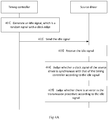
- Fig. 4A shows a method flow chart of still another data transmission method provided according to an embodiment, which data transmission method may be used in the implementation environment as shown in Fig. 1 .
- the data transmission method may include the following steps.
- the timing controller generates an idle signal, which is a random signal with a clock edge.
- the idle signal may carry at least two idle data successively arranged in a chronological order, there may be a clock edge between any two adjacent idle data in the at least two idle data, and each of the idle data is random data.
- Fig. 4B shows a flow chart of a method for generating an idle signal provided according to an embodiment. As shown in Fig. 4B , the method for generating an idle signal may include the following sub-steps.
- the timing controller acquires original idle data, which is pre-agreed by the timing controller and a source driver.
- the original idle data may be 8-bit data, in particular, may be binary data 00000000
- the timing controller may pre-agree on the original idle data with the source driver and store the original idle data, and when it is needed to generate an idle signal, the timing controller may read the original idle data stored by itself to realize acquisition of the original idle data.
- the bit digits of data are arranged in an order from low digit to high digit. For example, the arrangement order of data 10000010 is from right to left, that is, its first digit of data is 0, its last digit of data is 1, "1000" is its 4 low order digits, and "0010" is its 4 high order digits.
- the timing controller may interact with the source driver to agree on the original idle data, and an agreement procedure is, for example, but not limited to, that the timing controller sends an agreement instruction carrying the original idle data to the source driver, and after the source driver receives the agreement instruction, if the source driver agrees that the original idle data carried by the agreement instruction is employed to generate an idle signal, the source driver sends a response instruction carrying first indication information to the timing controller, which first indication information is used for indicating that the source driver agrees that the original idle data carried by the agreement instruction is employed to generate an idle signal, and thereby the agreement is successful; and if the source driver does not agree that the original idle data carried by the agreement instruction is employed to generate an idle signal, the source driver sends a response instruction carrying second indication information to the timing controller, which second indication information is used for indicating that the source driver does not agree that the original idle data carried by the agreement instruction is employed to generate an idle signal, and thereby the agreement fails; or, if the source driver does not agree
- the original idle data is binary data 00000000 is just exemplary, in a practical application, the original idle data may further be binary data 11111111, or the original idle data may further be any binary data consisting of 0 and 1, which will not be limited by the disclosure.
- the original idle data is set to binary data 00000000, and since the binary data 00000000 has not a flip edge, this may facilitate the timing controller and the source driver to process the original idle data.
- the source driver may be any of the source drivers 02, and the original idle data agreed on by the timing controller with a different source driver may be identical or different, which will not be limited by the disclosure.
- the timing controller performs pseudo-random processing on the original idle data to obtain random idle data.
- the timing controller may first generate a pseudo-random sequence and then scramble the original idle data employing the pseudo-random sequence, to implement pseudo-random processing of the original idle data.
- the timing controller may generate a pseudo-random sequence through a linear shift register, and the number of bit digits of the pseudo-random sequence may be equal to that of the original idle data.
- the timing controller may perform XOR processing on the pseudo-random sequence and the original idle data, to implement scrambling of the original idle data.
- the linear shift register has an initial data, and after the initial data is inputted to the linear shift register, the linear shift register may output a pseudo-random sequence by internal operations, wherein after the linear shift register is reset, it may generate a pseudo-random sequence based on the initial data, afterwards, the linear shift register may generate a new pseudo-random sequence taking the pseudo-random sequence outputted last time as an input, and so on.
- the linear shift register may output a new pseudo-random sequence based on the pseudo-random sequence outputted at the previous clock, wherein a specific implementation procedure in which the linear shift register generates a new pseudo-random sequence based on the inputted pseudo-random sequence may be referred to the related art, which will not be limited by the disclosure.
- the pseudo-random sequence generated by the linear shift register is 10001101
- random idle data 10001101 may be obtained by the timing controller performing XOR processing on the original idle data 00000000 and the pseudo-random sequence 10001101
- the random idle data is also 8-bit data.
- the timing controller encodes the random idle data to obtain first idle data, which is any of the at least two idle data in the idle signal.
- the random idle data is 8-bit data
- the first idle data may be 10-bit data
- the timing controller may encode the random idle data employing an 8b/10b encoding (i.e., encoding 8-bit data into 10-bit data) approach to obtain the first idle data.
- Fig. 4C shows a flow chart of a method for encoding random idle data provided according to an embodiment. As shown in Fig. 4C , the encoding method may include the following sub-steps.
- the random idle data is encoded according to a preset 8b/9b encoding mapping relationship to obtain encoded random idle data, which is 9-bit data.
- the timing controller may store a preset 8b/9b encoding (i.e., encoding 8-bit data into 9-bit data) mapping relationship, and the timing controller may encode the random idle data (8-bit data) according to the 8b/9b encoding mapping relationship to obtain encoded random idle data, which is 9-bit data.
- 8b/9b encoding mapping relationship stored by the timing controller may be as follows:
- the random idle data 10001101 is encoded according to the above 8b/9b encoding mapping relationship as an example, wherein the first digit of data to the eighth digit of data of the random idle data 10001101 are successively 1, 0, 1, 1, 0, 0, 0, 1, encoded random idle data may be obtained by encoding the random idle data 10001101 according to the above 8b/9b encoding mapping relationship, which encoded random idle data is 9-bit data 101000100, wherein in the encoded random idle data,
- clock flip digit processing is performed on the encoded random idle data and a bit indicating whether clock flip digit processing has been performed is added to obtain the first idle data.
- the timing controller may perform clock flip digit processing on the encoded random idle data and add an indication bit to obtain the first idle data, which is 10-bit data. For example, the timing controller may add a tenth digit of data behind the encoded random idle data, and cause the first idle data to have a clock flip digit, and the tenth digit of data may be used for indicating whether the first 9 digits of data of the first idle data have undergone the encoding of bit-by-bit reversion, in order that the first idle data can be correctly decoded subsequently.
- the tenth digit of data may be 0 or 1, and when the tenth digit of data of the first idle data is 1, the tenth digit of data indicates that the first 9 digits of data of the first idle data have undergone the encoding of bit-by-bit reversion, and when the tenth digit of data of the first idle data is 0, the tenth digit of data indicates that the first 9 digits of data of the first idle data have not undergone the encoding of bit-by-bit reversion.
- the idle data in terms of transmission time, is usually located behind the display data. Therefore, when performing clock flip digit processing on the encoded random idle data, the timing controller has already encoded the display data located in front of the encoded random idle data, that is, there is at least one data (display data or idle data) that has been encoded in front of the encoded random idle data. Since the data transmission procedure is encoded employing the 8b/10b encoding approach, the encoded data is usually 10-bit data.
- the timing controller may determine whether it is necessary to perform the encoding of bit-by-bit reversion on the encoded random idle data, and in turn determine a specific value of the tenth digit of data to be added, wherein the target data is data located in front of and adjacent to the encoded random idle data, and the target data may be display data, or may also be idle data.
- the timing controller may detect whether the first digit of data of the encoded random idle data is identical to the tenth digit of data of the target data, and when the first digit of data of the encoded random idle data is identical to the tenth digit of data of the target data, in order to have a clock edge between the first idle data and the target data, the timing controller may perform the encoding of bit-by-bit reversion on the encoded random idle data, and add a tenth digit of data behind the encoded random idle data to obtain the first idle data, and at this point, the value of the tenth digit of data is 1 and it is used for indicating that the first 9 digits of data of the first idle data have undergone the encoding of bit-by-bit reversion; and when the first digit of data of the encoded random idle data is different from the tenth digit of data of the target data, there is a clock edge between the first idle data and the target data, the timing controller does not need to perform the encoding of bit
- the encoded random idle data is 101000101, and assume that the target data is 0101000100. Since the first digit of data of the encoded random idle data is 1, and the tenth digit of data of the target data is 0, the first digit of data of the encoded random idle data is different from the tenth digit of data of the target data, and the timing controller directly adds a tenth digit of data 0 behind the encoded random idle data 101000101 to obtain the first idle data 0101000101.
- the encoded random idle data is 101000101, and assume that the target data is 1100100100.
- the timing controller Since the first digit of data of the encoded random idle data is 1, and the tenth digit of data of the target data is 1, the first digit of data of the encoded random idle data is identical to the tenth digit of data of the target data, and the timing controller performs the encoding of bit-by-bit reversion on the encoded random idle data 101000101 to obtain 010111010, and then adds a tenth digit of data 1 behind 010111010 to obtain the first idle data 1010111010.
- the timing controller generates the idle signal according to at least two first idle data.
- the timing controller may generate the idle signal according to at least two said idle data.
- the timing controller causes at least two idle data to be carried on the idle signal according to an order of transmission time of the at least two idle data.
- Fig. 4D shows a schematic diagram of a format of an idle signal provided according to an embodiment. As shown in Fig. 4D , multiple idle data IDLEs are carried on the idle signal, and each of the idle data IDLEs may be generated employing the sub-step 4011 to the sub-step 4013. Further, Fig. 4E shows a waveform diagram of an idle signal provided according to an embodiment. As shown in Fig. 4E , each idle data IDLE carried by the idle signal is random data, and there is a clock edge between any two adjacent idle data IDLEs. Exemplarily, Fig. 4F shows a waveform diagram of an idle signal provided by the related art. With reference to Fig. 4F , the idle signal may be a clock signal with a fixed frequency.
- the idle signal as shown in Fig. 4E is a random signal and does not easily form an energy spike, its electromagnetic radiation is small, and its transmission procedure does not easily affect the EMI characteristic of the display device.
- the idle data IDLEs as shown in Fig. 4E are just exemplary, each of the idle data IDLEs actually includes 10 bit digits according to the above description, and each of the idle data IDLEs may further be other random data, which will not be limited by the disclosure.
- the timing controller sends the idle signal to the source driver.
- the timing controller may send the idle signal to the source driver.
- the timing controller may send the idle signal as shown in Fig. 4E to the source driver.
- the data of each frame of image may include display data, clock data and idle data, the display data is carried on a display signal, the clock data is carried on a clock signal, and the idle data is carried on an idle signal, and the display data is used for image display, the clock data is used for clock recovery, and the idle data may be used for judging whether clocks are synchronous. From this, it can be seen that for each frame of image to be displayed, the timing controller needs to send a display signal, a clock signal and an idle signal to the source driver.
- the timing controller may send a data signal to the source driver, which data signal include a display signal, a clock signal and an idle signal, which clock signal is embedded in the display signal.
- the timing controller is coupled to the source driver via a data transmission line, and the timing controller may send the data signal to the source driver via the data transmission line.
- Fig. 4G shows a schematic diagram of a format of a data signal provided according to an embodiment.
- the data signal may include a display signal, a clock signal and an idle signal
- the display signal carries display data DATA
- the clock signal is embedded into the display signal (that is, clock data is embedded into the display data DATA)
- the idle signal carries idle data IDLE
- the time corresponding to each frame of image may include an idle time T blank
- the idle data IDLE is transmitted in the idle time T blank
- the idle data IDLE may be the idle data as shown in Fig. 4E .
- Fig. 4H shows a schematic diagram of a format of a data signal provided by the related art.
- Fig. 4H shows a schematic diagram of a format of a data signal provided by the related art.
- the data signal includes a display signal, a clock signal and an idle signal
- the display signal carries display data DATA
- the clock signal is embedded into the display signal
- the idle signal is transmitted in an idle time T blank
- the idle signal is a clock signal with a fixed frequency.
- the timing controller may send a data signal as shown in Fig. 4G to the source driver via a data transmission line.
- the idle signal is a random signal, it does not easily form an energy spike, its electromagnetic radiation is small, and its transmission procedure does not easily affect the EMI characteristic of a display device.
- the source driver receives the idle signal sent by the timing controller.
- the source driver may receive the idle signal sent by the timing controller.
- the source driver receives a data signal sent by the timing controller, which data signal includes a display signal, a clock signal and an idle signal, which clock signal is embedded into the display signal, wherein the idle signal is a random signal with a clock edge.
- the source driver receives a data signal as shown in Fig. 4G sent by the timing controller.
- the source driver judges whether a clock signal of the source driver is synchronous with that of the timing controller according to the idle signal.
- the source driver may judge whether a clock signal of the source driver is synchronous with that of the timing controller according to the idle signal.
- the source driver since what the source driver receives is a data signal including the idle signal, the source driver may first determine the idle signal from the data signal, and then judge whether the clock signal of the source driver is synchronous with that of the timing controller according to the idle signal.
- a procedure in which the source driver determines the idle signal from the data signal may be referred to the related art, which will not be limited by the disclosure.
- a method for the source driver to judge whether the clock signal of the source driver is synchronous with that of the timing controller according to the idle signal may be referred to Fig. 4I . With reference to Fig. 4I , the method may include the following sub-steps.
- the source driver acquires the clock edge of the idle signal.
- the source driver may acquire the clock edge of the idle signal.
- the clock edge of the idle signal is located between two adjacent idle data, and it can be seen from the description of the step 401 that, each of the idle data may be 10-bit data and there may be a clock edge between two adjacent idle data, the source driver may grab the idle signal in units of 10 bits to acquire clock edges of the idle signal, which will not be limited by the disclosure.
- the source driver judges whether the clock signal of the source driver is synchronous with that of the timing controller according to the clock edge of the idle signal.
- the source driver may recover the clock signal according to the clock edges of the idle signal, and then compare the clock signal of the source driver with the recovered clock signal, and if the clock signal of the source driver is the same as the recovered clock signal, then the clock signal of the source driver is synchronous with that of the timing controller, otherwise, the clock signal of the source driver is asynchronous with that of the timing controller.
- Fig. 4J is a comparison chart for a recovered clock signal and the clock signal of the source driver provided according to an embodiment.
- the clock signal 1 is a recovered clock signal
- the clock signal 2 is the clock signal of the source driver.
- the source driver compares the clock signal 1 with the clock signal 2, and may determine that the clock signal 1 is the same as the clock signal 2, and therefore, the source driver determines that the clock signal of the source driver is synchronous with that of the timing controller.
- this embodiment is illustrated taking that the clock signal of the source driver is the same as the recovered clock signal as an example, and when the clock signal of the source driver is different from the recovered clock signal, the source driver determines that the clock signal of the source driver is asynchronous with that of the timing controller, and at this point, the source driver may further perform error correction and calibration on the clock signal, and a specific implementation of this procedure may be referred to the related art, which will not be repeated here by the disclosure any longer.
- the source driver judges whether there is an error in the transmission procedure according to the idle signal.
- the source driver may judge whether there is an error in the transmission procedure according to the idle signal.
- the source driver may judge whether there is an error in the transmission procedure according to a first idle data, which first idle data may be any of the multiple idle data carried by the idle signal.
- Fig. 4K shows a flow chart of a method for judging whether there is an error in a signal transmission procedure according to a first idle data provided according to an embodiment. With reference to Fig. 4K , the method includes the following sub-steps.
- the first idle data is decoded to obtain decoded idle data.
- the source driver may decode the first idle data to obtain decoded idle data.
- the first idle data may be 10-bit data, and the first idle data is obtained by the timing controller performing 8b/10b encoding on random idle data, and therefore, the source driver may perform 8b/10b decoding on the first idle data to obtain decoded idle data.
- the timing controller first performs 8b/9b encoding on the random idle data, and then performs clock flip digit processing to obtain the first idle data.
- the source driver may first perform de-clock-flip-digit processing on the first idle data to obtain 9-bit encoded random idle data, and then decode the 9-bit encoded random idle data to obtain decoded idle data, the decoded idle data is 8-bit data, and the decoded idle data may be the random idle data at the step 401, wherein the tenth digit of data of the first idle data is used for indicating whether the first 9 digits of data of the first idle data have undergone the encoding of bit-by-bit reversion, and when the tenth digit of data of the first idle data is 1, the tenth digit of data of the first idle data indicates that the first 9 digits of data of the first idle data have undergone the encoding of bit-by-bit reversion, and when the tenth digit of data of the first idle data is 0, the tenth digit of data of the first idle data indicates that the first 9 digits of data of the first idle data have not undergone
- the source driver detects the tenth digit of data of the first idle data. If the tenth digit of data of the first idle data is 1, the source driver determines that the first 9 digits of data of the first idle data have undergone the encoding of bit-by-bit reversion, and hence the source driver may remove the tenth digit of data of the first idle data and perform digit-wise inversion on the first 9 digits of data of the first idle data to obtain 9-bit encoded random idle data.
- the source driver determines that the first 9 digits of data of the first idle data have not undergone the encoding of bit-by-bit reversion, and hence the source driver may remove the tenth digit of data of the first idle data and determine the first 9 digits of data of the first idle data as 9-bit encoded random idle data.
- the first idle data is 1010111010.
- the source driver removes the tenth digit of data of the first idle data and performs digit-wise inversion on the first 9 digits of data of the first idle data to obtain 9-bit encoded random idle data 101000101.
- the first idle data is 0101000101.
- the source driver removes the tenth digit of data of the first idle data and determines the first 9 digits of data of the first idle data as 9-bit encoded random idle data, which 9-bit encoded random idle data is 101000101.
- the source driver may store a preset 8b/9b decoding (i.e., decoding 9-bit data into 8-bit data) mapping relationship, and the source driver may decode the 9-bit encoded random idle data according to the 8b/9b decoding mapping relationship to obtain decoded idle data, which decoded idle data is 8-bit data.
- 8b/9b decoding mapping relationship stored by the source driver may be as follows:
- decoded idle data may be obtained by decoding the 9-bit encoded random idle data 101000101 according to the above 8b/9b decoding mapping relationship, which decoded idle data is 8-bit data 10001101, wherein in the decoded idle data,
- the decoded idle data is descrambled to obtain descrambled idle data.
- the source driver may descramble the decoded idle data to obtain descrambled idle data.
- the decoded idle data is 10001101, and the source driver descrambles the decoded idle data 10001101.
- the source driver may first generate a pseudo-random sequence, and then descramble the decoded idle data employing the pseudo-random sequence, wherein the source driver may generate the pseudo-random sequence by a linear shift register, and the number of bit digits of the pseudo-random sequence may be equal to that of the decoded idle data, and since the number of bit digits of the decoded idle data is 8, the number of bit digits of the pseudo-random sequence is also 8, that is, the pseudo-random sequence is 8-bit data, and the source driver may perform exclusive OR processing on the pseudo-random sequence and the decoded idle data, to implement descrambling of the original idle data.
- the linear shift register in the source driver may be the same as the linear shift register in the timing controller, and the clock signal of the timing controller is synchronous with that of the source driver.
- the linear shift register may output a new pseudo-random sequence based on the pseudo-random sequence outputted at the previous clock.
- the pseudo-random sequence produced by the source driver is the same as the pseudo-random sequence produced by the timing controller. Therefore, the scrambling and descrambling procedures in the embodiments provided by the disclosure may be to employ the same pseudo-random sequence and perform exclusive OR processing on it and the original idle data twice as a whole, and thus the descrambling may be realized to recover the original idle data.
- the source driver After obtaining the descrambled idle data, the source driver judge whether there is an error in the signal transmission procedure according to the descrambled idle data. In an embodiment, since the original idle data is pre-agreed by the timing controller and the source driver, the source driver may acquire the original idle data agreed on by it and the timing controller, and then judge whether the descrambled idle data is the same as the agreed original idle data. If the descrambled idle data is the same as the agreed original idle data, the source driver determines that there is no error in the signal transmission procedure. If the descrambled idle data is different from the original idle data, the source driver determines that there is an error in the signal transmission procedure, and the source driver may judge the accuracy of the received data based on this.
- the descrambled idle data is 00000000
- the original idle data agreed on by the source driver and the timing controller is 00000000
- the source driver may determine that the descrambled idle data is the same as the agreed original idle data by comparing the descrambled idle data with the agreed original idle data, and therefore, the source driver determines that there is no error in the signal transmission procedure.
- the descrambled idle data is 00010010
- the original idle data agreed on by the source driver and the timing controller is 00000000
- the source driver may determine that the descrambled idle data is different from the agreed original idle data by comparing the descrambled idle data with the agreed original idle data, and therefore, the source driver determines that there is an error in the signal transmission procedure. Further, the source driver may further determine the number of digits of bits for which the descrambled idle data and the agreed original idle data are different, and determine the transmission error rate according to the number of digits of bits.
- the source driver may further feed the transmission error rate back to the timing controller, in order that the timing controller determines whether signal retransmission is required, or the source driver may judge whether calibration, etc. is required for the signal according to the transmission error rate, and perform a subsequent calibration operation, etc., which will not be repeated here by the disclosure any longer.
- clock recovery is required at the receiving end (the source driver), and it is necessary to be ensured at any moment that the frequency and phase of the clock of the receiving end keep consistent (i.e., keep clock synchronization) with those of the sending end (the timing controller).
- the sending end transmits a clock signal with a fixed frequency to the receiving end in an idle time (also called blanking time), and according to this clock signal, the receiving end determines its own internal clock and the clock signal of the receiving end, causes the phase and frequency of the two to keep consistent, and corrects a deviation in time when the phase and frequency of the two are inconsistent.
- the drawback of such a signal transmission lies in that, for the overall system of a display device, in a certain period of time (blanking time), all that is transmitted on the data transmission line between the sending end and the receiving end is a signal of a fixed frequency, and the energy of the signal of the fixed frequency will be concentrated on a frequency point to form an energy spike, which will affect the EMI characteristic of the display device.
- a specially processed idle signal is employed to replace the clock signal with a fixed frequency, the specially processed idle signal is transmitted in the blanking time, the specially processed idle signal has clock edges, and the receiving end may acquire the clock signal of the sending end according to this feature of the idle signal, and judge the synchronization state of the clocks, and meanwhile, the idle signal is a random signal which has undergone pseudo-random processing, which can disperse the signal energy, thereby avoid the formation of an energy spike and improve the EMI characteristic of the display device.
- the 8-bit random idle data is converted into 10-bit idle data suitable for channel transmission and transmitted; due to undergoing the 8b/10b encoding, a clock edge jump is added to the random idle data (namely, including 0/1 flip), such that the idle signal has features of a clock edge, and as such, the receiving end can judge whether the clock signal of the sending end is synchronous with that of the receiving end based on this; and meanwhile, a fixed clock edge (a rising edge or a falling edge) will be formed between two adjacent idle data of the idle signal after the encoding, and thus the receiving end can judge whether the data phase of the sending end is consistent with that of the receiving end according to the fixed clock edge between two adjacent idle data.
- a clock edge jump is added to the random idle data (namely, including 0/1 flip), such that the idle signal has features of a clock edge, and as such, the receiving end can judge whether the clock signal of the sending end is synchronous with that of the receiving end based on this; and meanwhile, a fixed clock edge (a rising edge or a
- the source driver may judge whether clocks are synchronous according to the idle signal, which solves a problem of a poor anti-EMI capability of a display device due to an idle signal easily forming an energy spike, and improves the anti-EMI capability of the display device.
- Fig. 5A shows a block diagram of a timing controller 500 provided according to an embodiment, which timing controller 500 may be used for performing a data transmission method provided by the embodiment as shown in Fig. 2 or Fig. 4A .
- the timing controller 500 may include:
- the source driver may judge whether clocks are synchronous according to the idle signal, which solves a problem of a poor anti-EMI capability of a display device due to an idle signal easily forming an energy spike, and improves the anti-EMI capability of the display device.
- the idle signal carries at least two idle data successively arranged in a chronological order, there is a clock edge between any two adjacent idle data in the at least two idle data, and each of the idle data is random data.
- Fig. 5B shows a block diagram of a generator 510 provided according to an embodiment.
- the generator 510 may include:
- the processing unit 512 may further be configured for generating pseudo-random sequence, and scrambling the original idle data employing the pseudo-random sequence.
- the processing unit 512 may further be configured for generating pseudo-random sequence through a linear shift register.
- the number of bit digits of the pseudo-random sequence is equal to that of the original idle data
- the processing unit 512 may further be configured for performing XOR processing on the pseudo-random sequence and the original idle data.
- the random idle data is 8-bit data
- the first idle data is 10-bit data
- the encoding unit 513 may further be configured for encoding the random idle data employing an 8b/10b encoding approach to obtain the first idle data.
- the encoding unit 513 may further be configured for:
- the original idle data is binary data 00000000.
- the sender 520 may further be configured for sending a data signal to the source driver, the data signal including a display signal, a clock signal and an idle signal, and the clock signal is embedded into the display signal.
- the source driver may judge whether clocks are synchronous according to the idle signal, which solves a problem of a poor anti-EMI capability of a display device due to an idle signal easily forming an energy spike, and improves the anti-EMI capability of the display device.
- Fig. 6A shows a block diagram of a source driver 600 provided according to an embodiment, which source driver 600 may be used for performing a data transmission method provided by the embodiment as shown in Fig. 3 or Fig. 4A .
- the source driver 600 may include:
- the source driver since the idle signal is a random signal, the idle signal will not form an energy spike, and since the idle signal has a clock edge, the source driver may judge whether clocks are synchronous according to the idle signal, which solves a problem of a poor anti-EMI capability of a display device due to an idle signal easily forming an energy spike, and improves the anti-EMI capability of the display device.
- the synchronization judger 620 may further be configured for:
- the idle signal carries at least two idle data successively arranged in a chronological order, there is a clock edge between any two adjacent idle data in the at least two idle data, and each of the idle data is random data.
- the idle data is obtained by the timing controller scrambling original idle data to obtain random idle data and then encoding the random idle data
- the idle data is any of the at least two idle data in the received idle signal.
- Fig. 6B shows a block diagram of another source driver 600 provided according to an embodiment.
- the source driver 600 may further include:
- the original idle data is binary data 00000000.
- the receiver 610 may further be configured for receiving a data signal sent by the timing controller, which data signal includes a display signal, a clock signal and an idle signal, which clock signal is embedded into the display signal.
- the source driver since the idle signal is a random signal, the idle signal will not form an energy spike, and since the idle signal has a clock edge, the source driver may judge whether clocks are synchronous according to the idle signal, which solves a problem of a poor anti-EMI capability of a display device due to an idle signal easily forming an energy spike, and improves the anti-EMI capability of the display device.
- a display device including a timing controller and a source driver, and a way of connecting the two may be referred to Fig. 1 .
- the timing controller may be the timing controller 500 as shown in Fig. 5A
- the source driver may be the source driver 600 as shown in Fig. 6A or Fig. 6B .
- the display device may be any product or component with the display function, such as a liquid crystal display device, an electronic paper, an organic light emitting diode (OLED) panel, a mobile phone, a tablet computer, a television, a display, a notebook computer, a digital photo frame, a navigator, etc.
- a liquid crystal display device such as a liquid crystal display device, an electronic paper, an organic light emitting diode (OLED) panel, a mobile phone, a tablet computer, a television, a display, a notebook computer, a digital photo frame, a navigator, etc.
- OLED organic light emitting diode
- the above embodiments are just illustrated by division of the above various functional modules, and in a practical application, the above functions may be allocated to different functional modules for accomplishment as needed. It may be possible to divide the internal structure of a device into different functional modules to accomplish all or part of the above described functions. In addition, the function of one module described above may be accomplished by multiple modules, and the functions of multiple modules described above may also be integrated into one module for accomplishment.
- any reference sign placed between the parentheses shall not be construed as limiting to a claim.
- the term “include” does not exclude the presence of an element or a step other than those listed in a claim.
- the word “a” or “an” preceding an element does not exclude the presence of a plurality of such elements.
- one or more of the devices may be embodied by one and the same hardware item.
Landscapes
- Engineering & Computer Science (AREA)
- Physics & Mathematics (AREA)
- Theoretical Computer Science (AREA)
- General Physics & Mathematics (AREA)
- Computer Hardware Design (AREA)
- Computer Networks & Wireless Communication (AREA)
- Signal Processing (AREA)
- Crystallography & Structural Chemistry (AREA)
- Chemical & Material Sciences (AREA)
- Power Engineering (AREA)
- Multimedia (AREA)
- Computer Security & Cryptography (AREA)
- Spectroscopy & Molecular Physics (AREA)
- General Engineering & Computer Science (AREA)
- Control Of Indicators Other Than Cathode Ray Tubes (AREA)
Abstract
Description
- This application claims the priority of the Chinese patent application with the filing date of June 9, 2017 and the application number of
201710434614.4 - The disclosure relates to the field of data transmissions, and in particular, to a data transmission method, a timing controller, a source driver and a display device.
- A display device generally includes a display panel and a panel driving circuit for driving the display panel, the panel driving circuit includes a timing controller (Tcon for short), a gate driving circuit and a source driving circuit, wherein the gate driving circuit includes a plurality of gate drivers, and the source driving circuit includes a plurality of source drivers.
- The panel driving circuit usually adopts a point-to-point interface transmission mode to transmit a data signal. In the point-to-point interface transmission mode, the timing controller is coupled to the plurality of source drivers via a plurality of data transmission lines, each of the source drivers corresponds to a data transmission line, the timing controller may transmit a data signal to a corresponding source driver via the data transmission line, the data signal usually includes a display signal, a clock signal and an idle signal, the clock signal is usually embedded in the display signal, the idle signal is usually a clock signal with a fixed frequency, and after receiving the data signal, the source driver may recover the clock signal according to features of the data signal, sample the display signal according to the recovered clock signal and display an image based on a sampling result, and the source driver may further judge whether the recovered clock signal is synchronized with a clock signal inside the source driver according to the idle signal, wherein the display signal is used for carrying display data, which is used for displaying an image.
- The disclosure provides a data transmission method, a timing controller, a source driver and a display device.
- According to an aspect of the invention, there is provided a data transmission method for a timing controller, the timing controller being coupled to at least one source driver, the method including: generating an idle signal, which is a random signal with a clock edge; and sending the idle signal to a source driver, which source driver is any of the at least one source driver.
- In an embodiment, the idle signal carries at least two idle data successively arranged in a chronological order, there is a clock edge between any two adjacent idle data in the at least two idle data, and each of the idle data is random data.
- In an embodiment, the step of generating an idle signal may further include: acquiring original idle data, which is pre-agreed by the timing controller and the source driver; performing pseudo-random processing on the original idle data to obtain random idle data; encoding the random idle data to obtain first idle data, which is any of the at least two idle data; and generating the idle signal according to the at least two first idle data.
- In an embodiment, the step of performing pseudo-random processing on the original idle data may further include: generating a pseudo-random sequence; and scrambling the original idle data employing the pseudo-random sequence.
- In an embodiment, the number of bit digits of the pseudo-random sequence is equal to that of the original idle data, and the step of scrambling the original idle data employing the pseudo-random sequence may further include: performing XOR processing on the pseudo-random sequence and the original idle data.
- In an embodiment, the random idle data has a first length, and the first idle data has a second length that is at least 2 greater than the first length.
- In an embodiment, the random idle data is 8-bit data, the first idle data is 10-bit data, and the random idle data may be encoded employing an 8b/10b encoding approach to obtain the first idle data.
- In an embodiment, the step of encoding the random idle data to obtain first idle data may further include: encoding the random idle data according to a preset encoding mapping relationship to obtain encoded random idle data, of which the length is between the first length and the second length; and performing clock flip digit processing on the encoded random idle data and adding a bit indicating whether clock flip digit processing has been performed to obtain the first idle data.
- In an embodiment, it may be possible to encode the random idle data according to a preset 8b/9b encoding mapping relationship to obtain encoded random idle data, which is 9-bit data.
- According to another aspect of the disclosure, there is provided a data transmission method for a source driver, which source driver is any of at least one source driver coupled to a timing controller, the method including: receiving an idle signal sent by the timing controller, which idle signal is a random signal with a clock edge;
judging whether a clock signal of the source driver is synchronous with that of the timing controller according to the idle signal. - In an embodiment, the step of judging whether a clock signal of the source driver is synchronous with that of the timing controller according to the idle signal may further include:
acquiring the clock edge of the idle signal; and judging whether the clock signal of the source driver is synchronous with that of the timing controller according to the clock edge of the idle signal. - In an embodiment, the idle signal carries at least two idle data successively arranged in a chronological order, there is a clock edge between any two adjacent idle data in the at least two idle data, and each of the idle data is random data.
- In an embodiment, the idle data is obtained by the timing controller scrambling original idle data to obtain random idle data and then encoding the random idle data, and the method may further include: decoding the idle data to obtain decoded idle data; descrambling the decoded idle data to obtain descrambled idle data; and judging whether there is an error in the signal transmission procedure according to the descrambled idle data.
- In an embodiment, the original idle data is pre-agreed by the timing controller and the source driver, and the step of judging whether there is an error in the signal transmission procedure according to the descrambled idle data may further include: judging whether the descrambled idle data is the same as the original idle data; determining that there is no error in the signal transmission procedure if the descrambled idle data is the same as the original idle data; and determining that there is an error in the signal transmission procedure if the descrambled idle data is different from the original idle data.
- According to a further aspect of the invention, there is provided a timing controller, which is coupled to at least one source driver and which may include: a generator, which may be configured for generating an idle signal, which is a random signal with a clock edge; and a sender, which may be configured for sending the idle signal to a source driver, which source driver is any of the at least one source driver.
- In an embodiment, the idle signal carries at least two idle data successively arranged in a chronological order, there is a clock edge between any two adjacent idle data in the at least two idle data, and each of the idle data is random data.
- In an embodiment, the generator may further include: an acquisition unit, which may be configured for acquiring original idle data, which is pre-agreed by the timing controller and the source driver; a processing unit, which may be configured for performing pseudo-random processing on the original idle data to obtain random idle data; an encoding unit, which may be configured for encoding the random idle data to obtain first idle data, which is any of the at least two idle data; and a generation unit, which may be configured for generating the idle signal according to the at least two first idle data.
- In an embodiment, the processing unit may be configured for scrambling the original idle data employing the pseudo-random sequence.
- In an embodiment, the number of bit digits of the pseudo-random sequence is equal to that of the original idle data, and the processing unit may be configured for performing XOR processing on the pseudo-random sequence and the original idle data.
- In an embodiment, the random idle data has a first length, and the first idle data has a second length that is at least 2 greater than the first length.
- In an embodiment, the random idle data is 8-bit data, the first idle data is 10-bit data, and the encoding unit may be configured for encoding the random idle data employing an 8b/10b encoding approach to obtain the first idle data.
- In an embodiment, the encoding unit may be configured for encoding the random idle data according to a preset encoding mapping relationship to obtain encoded random idle data, of which the length is between the first length and the second length; and performing clock flip digit processing on the encoded random idle data and adding a bit indicating whether clock flip digit processing has been performed to obtain the first idle data.
- In an embodiment, the encoding unit may be configured for encoding the random idle data according to a preset 8b/9b encoding mapping relationship to obtain encoded random idle data, which is 9-bit data.
- According to a further aspect of the disclosure, there is provided a source driver, which is any of at least one source driver coupled to a timing controller and which includes: a receiver, which may be configured for receiving an idle signal sent by the timing controller, which idle signal is a random signal with a clock edge; and a synchronization judger, which may be configured for judging whether a clock signal of the source driver is synchronous with that of the timing controller according to the idle signal.
- In an embodiment, the synchronization judger may further be configured for: acquiring the clock edge of the idle signal; and judging whether the clock signal of the source driver is synchronous with that of the timing controller according to the clock edge of the idle signal.
- In an embodiment, the idle signal carries at least two idle data successively arranged in a chronological order, there is a clock edge between any two adjacent idle data in the at least two idle data, and each of the idle data is random data.
- In an embodiment, the idle data is obtained by the timing controller scrambling original idle data to obtain random idle data and then encoding the random idle data, and the source driver may further include: a decoder, which may be configured for decoding the idle data to obtain decoded idle data; a descrambler, which may be configured for descrambling the decoded idle data to obtain descrambled idle data; and a transmission judger, which may be configured for judging whether there is an error in the signal transmission procedure according to the descrambled idle data.
- According to a further aspect of the disclosure, there is provided a display device including any of the timing controllers as described above and a plurality of source drivers of the kind of any of the source drivers as described above.
- This Summary introduces some concepts of the invention in a simplified form that are further described below in the Detailed Description. This Summary is not intended to give necessary features or essential features of the claimed subject matter, nor is it intended to limit the scope of the claimed subject matter. In addition, as described herein, various other features and advantages may also be incorporated into the techniques as needed.
- In order to more clearly illustrate the technical solutions of some embodiments of the disclosure, the disclosure provides the following appended drawings to be used in the description of the embodiments. It should be appreciated that, the drawings in the following description only relate to some embodiments, and for the person having ordinary skills in the art, other drawings may also be obtained according to these drawings under the premise of not paying out undue experimentation, which other drawings also fall within the scope of the invention.
-
Fig. 1 is a schematic diagram of an application environment of a data transmission method provided according to an embodiment; -
Fig. 2 is a method flow chart of a data transmission method provided according to an embodiment; -
Fig. 3 is a method flow chart of another data transmission method provided according to an embodiment; -
Fig. 4A is a method flow chart of still another data transmission method provided according to an embodiment; -
Fig. 4B is a flow chart of a method for generating an idle signal provided according to an embodiment; -
Fig. 4C is a flow chart of a method for encoding random idle data provided according to an embodiment; -
Fig. 4D is a schematic diagram of a format of an idle signal provided according to an embodiment; -
Fig. 4E is a waveform diagram of an idle signal provided according to an embodiment; -
Fig. 4F is a waveform diagram of an idle signal provided by the related art; -
Fig. 4G is a schematic diagram of a data signal provided according to an embodiment; -
Fig. 4H is a schematic diagram of a data signal provided by the related art; -
Fig. 4I is a flow chart of a method for judging whether a clock signal of the source driver is synchronous with that of the timing controller provided according to an embodiment; -
Fig. 4J is a comparison chart for clock signals provided according to an embodiment; -
Fig. 4K is a flow chart of a method for judging whether there is an error in a signal transmission procedure provided according to an embodiment; -
Fig. 5A is a block diagram of a timing controller provided according to an embodiment; -
Fig. 5B is a block diagram of a generator provided according to an embodiment; -
Fig. 6A is a block diagram of a source driver provided according to an embodiment; and -
Fig. 6B is a block diagram of another source driver provided according to an embodiment. - The drawings herein are incorporated into the specification and constitute a part of the specification, show embodiments in accordance with the invention, and are used for explaining the principle of the invention along with the specification.
- To be able to more clearly understand the objects, technical solutions and advantages of some embodiments, in the following, the embodiments will be further described in detail in conjunction with the drawings. It can be appreciated by the person having ordinary skills in the art that, the described embodiments are just a part of embodiments of the disclosure, and not all the embodiments. Based on the embodiments in the disclosure, all the other embodiments obtained by the person having ordinary skills in the art under the premise of not paying out undue experimentation pertain to the scope protected by the invention.
-
Fig. 1 shows a schematic diagram of an application environment of a data transmission method provided according to an embodiment. With reference toFig. 1 , the data transmission method may be applied in a display device (not shown inFig. 1 ), the display device may include a display panel (not shown inFig. 1 ) and a panel driving circuit (not shown inFig. 1 ) for driving the display panel, the panel driving circuit (not shown inFig. 1 ) may include a timing controller 01, a gate driving circuit (not shown inFig. 1 ) and a source driving circuit, wherein the gate driving circuit may include a plurality of gate drivers (not shown inFig. 1 ), and the source driving circuit may include a plurality ofsource drivers 02. The timing controller 01 is coupled to the plurality ofsource drivers 02 via a plurality of data transmission lines (not shown inFig. 1 ), each of thesource drivers 02 corresponds to a data transmission line, the timing controller 01 may transmit a data signal to acorresponding source driver 02 via a data transmission line, and the data signal usually may include a display signal, a clock signal and an idle signal. -
Fig. 2 shows a method flow chart of a data transmission method provided according to an embodiment. The data transmission method may be used in the timing controller 01 in the implementation environment as shown inFig. 1 , in which the timing controller 01 is coupled to the plurality ofsource drivers 02, respectively. As shown inFig. 2 , the data transmission method may include: -
step 201, generating an idle signal, which is a random signal with a clock edge; and -
step 202, sending the idle signal to a source driver, which source driver is any of the plurality of source drivers. It is noted that, although the plurality ofsource drivers 02 are shown inFig. 1 , the data transmission method is equally adapted for communicating a data signal only to onesource driver 02. - From the above, since the idle signal is a random signal, the idle signal will not form an energy spike, and since the idle signal has a clock edge, the source driver may judge whether clocks are synchronous according to the idle signal, which solves a problem of a poor anti-EMI capability of a display device due to an idle signal easily forming an energy spike, and improves the anti-EMI capability of the display device.
- In an embodiment, the idle signal carries at least two idle data successively arranged in a chronological order, there is a clock edge between any two adjacent idle data in the at least two idle data, and each of the idle data is random data.
- In an embodiment, the step of generating an idle signal may include:
- acquiring original idle data, which is pre-agreed by the timing controller and the source driver;
- performing pseudo-random processing on the original idle data to obtain random idle data;
- encoding the random idle data to obtain first idle data, which is any of the at least two idle data; and
- generating the idle signal according to at least two first idle data.
- In an embodiment, the step of performing pseudo-random processing on the original idle data may include:
- generating a pseudo-random sequence; and
- scrambling the original idle data employing the pseudo-random sequence.
- In an embodiment, the step of generating a pseudo-random sequence may include: generating a pseudo-random sequence through a linear shift register.
- In an embodiment, the number of bit digits of the pseudo-random sequence is equal to that of the original idle data, and the step of scrambling the original idle data employing the pseudo-random sequence may include: performing XOR processing on the pseudo-random sequence and the original idle data.
- In an embodiment, the random idle data is 8-bit data, the first idle data is 10-bit data, and the step of encoding the random idle data to obtain first idle data may include: encoding the random idle data employing an 8b/10b encoding approach to obtain the first idle data. It is noted that, although the 8b/10b encoding approach is employed in this example, in other embodiments, it may even be possible to employ random idle data of a different length and first idle data of a different length. Accordingly, it may also be possible to employ other different encoding approaches, and the disclosure is not limited to the 8b/10b encoding approach.
- In an embodiment, the step of encoding the random idle data employing an 8b/10b encoding approach to obtain the first idle data may include:
- encoding the random idle data according to a preset encoding mapping relationship to obtain encoded random idle data, of which the length is between the first length of the random idle data and the second length of the first idle data, wherein for example, a preset 8b/9b encoding mapping relationship may be employed, and the thus obtained encoded random idle data is 9-bit data; and
- performing clock flip digit processing on the encoded random idle data and adding a bit indicating whether clock flip digit processing has been performed to obtain the first idle data.
- In a specific implementation, the original idle data is binary data 00000000.
- In an embodiment, the step of sending the idle signal to a source driver may include: sending a data signal to the source driver, which data signal includes a display signal, a clock signal and an idle signal, which clock signal is embedded into the display signal.
- All the above embodiments may be combined in any form to form further embodiments of the invention, which will not be repeated here one by one any longer.
- From the above, in the data transmission method provided according to some embodiments of the invention, since the idle signal is a random signal, the idle signal will not form an energy spike, and since the idle signal has a clock edge, the source driver may judge whether clocks are synchronous according to the idle signal, which solves a problem of a poor anti-EMI capability of a display device due to an idle signal easily forming an energy spike, and improves the anti-EMI capability of the display device.
-
Fig. 3 shows a method flow chart of another data transmission method provided according to an embodiment. The data transmission method may be used in a source driver, the source driver may be any of thesource drivers 02 in the implementation environment as shown inFig. 1 , and the source driver is coupled to the timing controller 01. As shown inFig. 3 , the data transmission method may include:step 301, receiving an idle signal sent by the timing controller, which idle signal is a random signal with a clock edge; and step 302, judging whether a clock signal of the source driver is synchronous with that of the timing controller according to the idle signal. - In the above data transmission method, since the idle signal is a random signal, the idle signal will not form an energy spike, and since the idle signal has a clock edge, the source driver may judge whether clocks are synchronous according to the idle signal, which solves a problem of a poor anti-EMI capability of a display device due to an idle signal easily forming an energy spike, and improves the anti-EMI capability of the display device.
- In an embodiment, the step of judging whether a clock signal of the source driver is synchronous with that of the timing controller according to the idle signal may include:
- acquiring the clock edge of the idle signal; and
- judging whether the clock signal of the source driver is synchronous with that of the timing controller according to the clock edge of the idle signal.
- In an embodiment, the idle signal carries at least two idle data successively arranged in a chronological order, there is a clock edge between any two adjacent idle data in the at least two idle data, and each of the idle data is random data.
- In an embodiment, the idle data is obtained by the timing controller scrambling original idle data to obtain random idle data and then encoding the random idle data, the idle data is just any of the at least two idle data, and after the receiving an idle signal sent by the timing controller, the data transmission method may further include:
- decoding the idle data to obtain decoded idle data;
- descrambling the decoded idle data to obtain descrambled idle data; and
- judging whether there is an error in the signal transmission procedure according to the descrambled idle data.
- In an embodiment, the original idle data is pre-agreed by the timing controller and the source driver, and the step of judging whether there is an error in the signal transmission procedure according to the descrambled idle data may include:
- judging whether the descrambled idle data is the same as the original idle data;
- determining that there is no error in the signal transmission procedure if the descrambled idle data is the same as the original idle data; and
- determining that there is an error in the signal transmission procedure if the descrambled idle data is different from the original idle data.
- In an embodiment, the original idle data is binary data 00000000.
- In an embodiment, the step of receiving an idle signal sent by the timing controller may include: receiving a data signal sent by the timing controller, which data signal includes a display signal, a clock signal and an idle signal, which clock signal is embedded into the display signal.
- All the above embodiments may be combined in any manner to form further embodiments of the invention, which will not be repeated here one by one any longer.
- In the above data transmission method, since the idle signal is a random signal, the idle signal will not form an energy spike, and since the idle signal has a clock edge, the source driver may judge whether clocks are synchronous according to the idle signal, which solves a problem of a poor anti-EMI capability of a display device due to an idle signal easily forming an energy spike, and improves the anti-EMI capability of the display device.
-
Fig. 4A shows a method flow chart of still another data transmission method provided according to an embodiment, which data transmission method may be used in the implementation environment as shown inFig. 1 . As shown inFig. 4A , the data transmission method may include the following steps. - At step 401, the timing controller generates an idle signal, which is a random signal with a clock edge.
- Therein, the idle signal may carry at least two idle data successively arranged in a chronological order, there may be a clock edge between any two adjacent idle data in the at least two idle data, and each of the idle data is random data.
Fig. 4B shows a flow chart of a method for generating an idle signal provided according to an embodiment. As shown inFig. 4B , the method for generating an idle signal may include the following sub-steps. - At sub-step 4011, the timing controller acquires original idle data, which is pre-agreed by the timing controller and a source driver.
- Therein, the original idle data may be 8-bit data, in particular, may be binary data 00000000, the timing controller may pre-agree on the original idle data with the source driver and store the original idle data, and when it is needed to generate an idle signal, the timing controller may read the original idle data stored by itself to realize acquisition of the original idle data. It is noted that, in this example, the bit digits of data are arranged in an order from low digit to high digit. For example, the arrangement order of data 10000010 is from right to left, that is, its first digit of data is 0, its last digit of data is 1, "1000" is its 4 low order digits, and "0010" is its 4 high order digits.
- In an embodiment, before the timing controller acquires original idle data, the timing controller may interact with the source driver to agree on the original idle data, and an agreement procedure is, for example, but not limited to, that the timing controller sends an agreement instruction carrying the original idle data to the source driver, and after the source driver receives the agreement instruction, if the source driver agrees that the original idle data carried by the agreement instruction is employed to generate an idle signal, the source driver sends a response instruction carrying first indication information to the timing controller, which first indication information is used for indicating that the source driver agrees that the original idle data carried by the agreement instruction is employed to generate an idle signal, and thereby the agreement is successful; and if the source driver does not agree that the original idle data carried by the agreement instruction is employed to generate an idle signal, the source driver sends a response instruction carrying second indication information to the timing controller, which second indication information is used for indicating that the source driver does not agree that the original idle data carried by the agreement instruction is employed to generate an idle signal, and thereby the agreement fails; or, if the source driver does not agree that the original idle data carried by the agreement instruction is employed to generate an idle signal, the source driver may also not send a response instruction to the timing controller, and at this point, the timing controller and the source driver may agree on a preset duration of receiving a response instruction in advance, and if the timing controller does not receive a response instruction sent by the source driver within the preset duration after the agreement instruction was issued, the timing controller may determine that the source driver does not agree that the original idle data carried by the agreement instruction is employed to generate an idle signal, and determine that the agreement fails.
- It is noted that, that the original idle data is binary data 00000000 is just exemplary, in a practical application, the original idle data may further be binary data 11111111, or the original idle data may further be any binary data consisting of 0 and 1, which will not be limited by the disclosure. In this example, the original idle data is set to binary data 00000000, and since the binary data 00000000 has not a flip edge, this may facilitate the timing controller and the source driver to process the original idle data. The source driver may be any of the
source drivers 02, and the original idle data agreed on by the timing controller with a different source driver may be identical or different, which will not be limited by the disclosure. - At sub-step 4012, the timing controller performs pseudo-random processing on the original idle data to obtain random idle data.
- In particular, the timing controller may first generate a pseudo-random sequence and then scramble the original idle data employing the pseudo-random sequence, to implement pseudo-random processing of the original idle data. In an embodiment, the timing controller may generate a pseudo-random sequence through a linear shift register, and the number of bit digits of the pseudo-random sequence may be equal to that of the original idle data. In this example, since the number of bit digits of the original idle data is 8, the number of bit digits of the pseudo-random sequence is also 8, that is, the pseudo-random sequence is 8-bit data, and the timing controller may perform XOR processing on the pseudo-random sequence and the original idle data, to implement scrambling of the original idle data.
- In a specific implementation, the linear shift register has an initial data, and after the initial data is inputted to the linear shift register, the linear shift register may output a pseudo-random sequence by internal operations, wherein after the linear shift register is reset, it may generate a pseudo-random sequence based on the initial data, afterwards, the linear shift register may generate a new pseudo-random sequence taking the pseudo-random sequence outputted last time as an input, and so on. In a practical application, each time a clock passes, the linear shift register may output a new pseudo-random sequence based on the pseudo-random sequence outputted at the previous clock, wherein a specific implementation procedure in which the linear shift register generates a new pseudo-random sequence based on the inputted pseudo-random sequence may be referred to the related art, which will not be limited by the disclosure. Assume that the pseudo-random sequence generated by the linear shift register is 10001101, random idle data 10001101 may be obtained by the timing controller performing XOR processing on the original idle data 00000000 and the pseudo-random sequence 10001101, and the random idle data is also 8-bit data.
- By generating a pseudo-random sequence by the linear shift register and scrambling the original idle data according to the pseudo-random sequence, exactly the same original idle data may be scattered, such that it has certain randomness, and as such, in a subsequent procedure of signal transmission, signal energy may be dispersed randomly to all the frequency points, thereby avoiding the formation of an energy spike.
- At sub-step 4013, the timing controller encodes the random idle data to obtain first idle data, which is any of the at least two idle data in the idle signal.
- In this embodiment, the random idle data is 8-bit data, the first idle data may be 10-bit data, and the timing controller may encode the random idle data employing an 8b/10b encoding (i.e., encoding 8-bit data into 10-bit data) approach to obtain the first idle data. Exemplarily, reference is made to
Fig. 4C , which shows a flow chart of a method for encoding random idle data provided according to an embodiment. As shown inFig. 4C , the encoding method may include the following sub-steps. - At
sub-step 40131, the random idle data is encoded according to a preset 8b/9b encoding mapping relationship to obtain encoded random idle data, which is 9-bit data. - The timing controller may store a preset 8b/9b encoding (i.e., encoding 8-bit data into 9-bit data) mapping relationship, and the timing controller may encode the random idle data (8-bit data) according to the 8b/9b encoding mapping relationship to obtain encoded random idle data, which is 9-bit data. Therein, the 8b/9b encoding mapping relationship stored by the timing controller may be as follows:
              enc[0]=d[3];
              enc[1]=(∼d[2]&d[1])|(d[2]&d[1]&∼d[3])|(∼d[2]&∼d[0]);
              enc[2]=(d[2]&∼d[1])|(d[2]&d[1]&∼d[3])|(∼d[1]&d[0]);
              enc[3]=d[5];
              enc[4]=d[6];
              enc[5]=(∼d[2]&∼d[1]&∼d[4])|(d[2]&∼d[0])|(d[1]&∼d[0]);
              enc[6]=(∼d[2]&∼d[1]&∼d[4])|(d[2]&d[0])|(d[1]&d[0]);
              enc[7]=d[4];
              enc[8]=d[7];
wherein enc[i] is the (i+1)-th digit of data in the 9-bit data, 8≥i≥0, and i is an integer; d[j] is the (j+1)-th digit of data in the 8-bit data, 7≥j≥0, and j is an integer; and ∼ represents performing an inversion operation, & represents performing an AND operation, and | represents performing an OR operation. Therein, the inversion operation represents performing an inversion operation on a binary number, for example, the result of performing an inversion operation on the the first digit of data enc[0]=d[3]=1;
the second digit of data enc[1] = (∼d[2]&d[1])|(d[2]&d[1]&∼d[3])
|(∼d[2]&∼d[0]) = (∼1&0)|(1&0&∼1)|(∼1&∼1) = (0&0)|(1&0&0)|(0&0) = 0|0|0 = 0;
the third digit of data enc[2] = (d[2]&∼d[1])|(d[2]&d[1]&∼d[3])|
(∼d[1]&d[0]) = (1&∼0)|(1&0&∼1)|(∼0&1) = (1&1)|(1&0&0)|(1&1) = 1|0|1 = 1;
the fourth digit of data enc[3]=d[5]=0;
the fifth digit of data enc[4]=d[6]=0;
the sixth digit of data enc[5] = (∼d[2]&∼d[1]&∼d[4])|(d[2]&∼d[0])|
(d[1]&∼d[0]) = (∼1&∼0&∼0)|(1&∼1)|(0&∼1) = (0&1&1)|(1&0)|(0&0) = 0|0|0 =0;
the seventh digit of data enc[6] = (∼d[2]&∼d[1]&∼d[4])|(d[2]&d[0])|
(d[1]&d[0]) = (∼1&∼0&∼0)|(1&1)|(0&1) = (0&1&1)|(1&1)|(0&1) = 0|1|0 = 1;
the eighth digit of data enc[7]=d[4]=0;
the ninth digit of data enc[8]=d[7]=1.
              Dout[7]=d_code[8];
              Dout[6]=d_code[4];
              Dout[5]=d_code[3];
              Dout[4]=d_code[7];
              Dout[3]=d_code[0];
              Dout[2]=(d_code[6]^d_code[5])&∼(∼d_code[2]&d_code[1]);
              Dout[1]=(d_code[6]^d_code[5])&∼(d_code[2]&∼d_code[1]);
              Dout[0]=(d_code[6]&∼d_code[5])|(d_code[6]&d_code[5]&d_code[2])|(∼d_co
              de[6]&∼d_code[5]&d_code[2]);
wherein d_code[i] is the (i+1)-th digit in the 9-bit data, 8≥i≥0, and i is an integer; Dout[j] is the (j+1)-th digit in the 8-bit data, 7≥j≥0, and j is an integer; and ∧ represents performing an exclusive OR operation, ∼ represents performing an inversion operation, & represents performing an AND operation, and | represents performing an OR operation. Therein, explanation of the inversion operation, the AND operation and the OR operation may be referred to the step 401, performing an exclusive OR operation represents performing an exclusive OR operation on two binary numbers, and its rule is that the result of performing the exclusive OR operation is true when the two binary numbers are different, wherein true is 1, false is 0, and then 1∧1=0, 1∧0=1, 0∧1=1, 1∧1=0.
              the eighth digit of data Dout[7]=d_code[8]=1;
              the seventh digit of data Dout[6]=d_code[4]=0;
              the sixth digit of data Dout[5]=d_code[3]=0;
              the fifth digit of data Dout[4]=d_code[7]=0;
              the fourth digit of data Dout[3]=d_code[0]=1;
              the third digit of data Dout[2] = (d_code[6]^d_code[5])&∼
              (∼d_code[2]&d_code[1]) = (1^0)&∼(∼1&0) = (1^0)&∼(0&0) = 1&-0 = 1&1 = 1;
              the second digit of data Dout[1] = (d_code[6]^d_code[5])&∼
              (d_code[2]&∼d_code[1]) = (1^0)&∼(1&∼0) = (1^0)&∼(1&1) = 1&∼1 = 1&0 = 0;
              the first digit of data Dout[0] = (d_code[6]&∼d_code[5])|(d_code[6]&
              d_code[5]&d_code[2])|(∼d_code[6]&∼d_code[5]&d_code[2]) = (1&∼0)|(1&0&1)|
              (∼1&∼0&1) = (1&1)|(1&0&1)|(0&1&1) = 1|0|0 = 1.
- a
generator 510, which may be configured for generating an idle signal, which is a random signal with a clock edge; and - a
sender 520, which may be configured for sending the idle signal to a source driver, which source driver is any of a plurality of source drivers.
- an
acquisition unit 511, which may be configured for acquiring original idle data, which is pre-agreed by the timing controller and the source driver; - a
processing unit 512, which may be configured for performing pseudo-random processing on the original idle data to obtain random idle data; - an
encoding unit 513, which may be configured for encoding the random idle data to obtain first idle data, which is any of the at least two idle data in the idle signal; and - a
generation unit 514, which may be configured for generating the idle signal according to at least two first idle data.
- encoding the random idle data according to a preset 8b/9b encoding mapping relationship to obtain encoded random idle data, which is 9-bit data; and
- performing clock flip digit processing on the encoded random idle data and adding a bit indicating whether clock flip digit processing has been performed to obtain the first idle data.
- a
receiver 610, which may be configured for receiving an idle signal sent by the timing controller, which idle signal is a random signal with a clock edge; and - a
synchronization judger 620, which may be configured for judging whether a clock signal of the source driver is synchronous with that of the timing controller according to the idle signal.
- acquiring the clock edge of the idle signal; and
- judging whether the clock signal of the source driver is synchronous with that of the timing controller according to the clock edge of the idle signal.
- a
decoder 630, which may be configured for decoding the idle data to obtain decoded idle data; - a
descrambler 640, which may be configured for descrambling the decoded idle data to obtain descrambled idle data; and - a
transmission judger 650, which may be configured for judging whether there is an error in the signal transmission procedure according to the descrambled idle data. - In an embodiment, the original idle data is pre-agreed by the timing controller and the source driver,
- the
transmission judger 650 may further be configured for:- judging whether the descrambled idle data is the same as the original idle data;
- determining that there is no error in the signal transmission procedure if the descrambled idle data is the same as the original idle data; and
- determining that there is an error in the signal transmission procedure if the descrambled idle data is different from the original idle data.
Claims (26)
- A data transmission method for a timing controller, the timing controller being coupled to at least one source driver, the method comprising:generating an idle signal, which is a random signal with a clock edge; andsending the idle signal to a source driver, which source driver is any of the at least one source driver.
- The method as claimed in claim 1, wherein the idle signal carries at least two idle data successively arranged in a chronological order, there is a clock edge between any two adjacent idle data in the at least two idle data, and each of the idle data is random data.
- The method as claimed in claim 2, wherein the step of generating an idle signal comprises:acquiring original idle data, which is pre-agreed by the timing controller and the source driver;performing pseudo-random processing on the original idle data to obtain random idle datacompris;encoding the random idle data to obtain first idle data, which is any of the at least two idle data; andgenerating the idle signal according to at least two first idle data.
- The method as claimed in claim 3, wherein the step of performing pseudo-random processing on the original idle data comprises:generating a pseudo-random sequence; andscrambling the original idle data employing the pseudo-random sequence.
- The method as claimed in claim 4, wherein the number of bit digits of the pseudo-random sequence is equal to that of the original idle data, and the step of scrambling the original idle data employing the pseudo-random sequence comprises: performing XOR processing on the pseudo-random sequence and the original idle data.
- The method as claimed in claim 3, wherein the random idle data has a first length, and the first idle data has a second length that is at least 2 greater than the first length.
- The method as claimed in claim 3, wherein the random idle data is 8-bit data, the first idle data is 10-bit data, and the encoding the random idle data to obtain first idle data comprises: encode the random idle data employing an 8b/10b encoding approach to obtain the first idle data.
- The method as claimed in claim 7, wherein the step of encoding the random idle data to obtain first idle data comprises:encoding the random idle data according to a preset encoding mapping relationship to obtain encoded random idle data, of which the length is between the first length and the second length; andperforming clock flip digit processing on the encoded random idle data and adding a bit indicating whether clock flip digit processing has been performed to obtain the first idle data.
- A data transmission method for a source driver, which source driver is any of at least one source driver coupled to a timing controller, the method comprising:Receiving an idle signal sent by the timing controller, which idle signal is a random signal with a clock edge;Judging whether a clock signal of the source driver is synchronous with that of the timing controller according to the idle signal.
- The method as claimed in claim 9, wherein the step of judging whether a clock signal of the source driver is synchronous with that of the timing controller according to the idle signal further comprises:acquiring the clock edge of the idle signal; andjudging whether the clock signal of the source driver is synchronous with that of the timing controller according to the clock edge of the idle signal.
- The method as claimed in claim 9, wherein the idle signal carries at least two idle data successively arranged in a chronological order, there is a clock edge between any two adjacent idle data in the at least two idle data, and each of the idle data is random data.
- The method as claimed in claim 11, wherein the idle data is obtained by the timing controller scrambling original idle data to obtain random idle data and then encoding the random idle data, and the method furs:Decoding the idle data to obtain decoded idle data;Descrambling the decoded idle data to obtain descrambled idle data; andjudging whether there is an error in the signal transmission procedure according to the descrambled idle data.
- The method as claimed in claim 12, wherein the original idle data is pre-agreed by the timing controller and the source driver, and the step of judging whether there is an error in the signal transmission procedure according to the descrambled idle s:judging whether the descrambled idle data is the same as the original idle data;determining that there is no error in the signal transmission procedure if the descrambled idle data is the same as the original idle data; anddetermining that there is an error in the signal transmission procedure if the descrambled idle data is different from the original idle data.
- A timing controller, wherein the timing controller is coupled to at least one source driver and the timing controller comprises:a generator configured for generating an idle signal, which is a random signal with a clock edge; anda sender configured for sending the idle signal to a source driver, which source driver is any of the at least one source driver.
- The timing controller as claimed in claim 14, wherein the idle signal carries at least two idle data successively arranged in a chronological order, there is a clock edge between any two adjacent idle data in the at least two idle data, and each of the idle data is random data.
- The timing controller as claimed in claim 15, wherein
the generator further comprises:an acquisition unit configured for acquiring original idle data, which is pre-agreed by the timing controller and the source driver;a processing unit configured for performing pseudo-random processing on the original idle data to obtain random idle data;an encoding unit configured for encoding the random idle data to obtain first idle data, which is any of the at least two idle data; anda generation unit configured for generating the idle signal according to the at least two first idle data. - The timing controller as claimed in claim 16, wherein the processing unit is configured for scrambling the original idle data employing the pseudo-random sequence.
- The timing controller as claimed in claim 17, wherein the number of bit digits of the pseudo-random sequence is equal to that of the original idle data, and the processing unit is configured for performing XOR processing on the pseudo-random sequence and the original idle data.
- The timing controller as claimed in claim 16, wherein the random idle data has a first length, and the first idle data has a second length that is at least 2 greater than the first length.
- The timing controller as claimed in claim 16, characterized in that, the random idle data is 8-bit data, the first idle data is 10-bit data, and the encoding unit is used for encoding the random idle data employing an 8b/10b encoding approach to obtain the first idle data.
- The timing controller as claimed in claim 20, wherein
the encoding unit is configured for:encoding the random idle data according to a preset 8b/10b encoding mapping relationship to obtain encoded random idle data, which is 9-bit data; andperforming clock flip digit processing on the encoded random idle data and adding a bit indicating whether clock flip digit processing has been performed to obtain the first idle data. - A source driver, wherein the source driver is any of at least one source driver coupled to a timing controller and the source driver comprises:a receiver configured for receiving an idle signal sent by the timing controller, which idle signal is a random signal with a clock edge; anda synchronization judger configured for judging whether a clock signal of the source driver is synchronous with that of the timing controller according to the idle signal.
- A source driver as claimed in claim 22, wherein
the synchronization judger is further configured for:acquiring the clock edge of the idle signal; andjudging whether the clock signal of the source driver is synchronous with that of the timing controller according to the clock edge of the idle signal. - A source driver as claimed in claim 22, wherein the idle signal carries at least two idle data successively arranged in a chronological order, there is a clock edge between any two adjacent idle data in the at least two idle data, and each of the idle data is random data.
- A source driver as claimed in claim 24, wherein the idle data is obtained by the timing controller scrambling original idle data to obtain random idle data and then encoding the random idle data, and the source driver further comprises:a decoder configured for decoding the idle data to obtain decoded idle data;a descrambler configured for descrambling the decoded idle data to obtain descrambled idle data; anda transmission judger configured for judging whether there is an error in the signal transmission procedure according to the descrambled idle data.
- A display device, wherein the display device comprises a timing controller as claimed in any of claims 14-21 and a plurality of source drivers as claimed in any of claims 22-25.
Applications Claiming Priority (2)
| Application Number | Priority Date | Filing Date | Title |
|---|---|---|---|
| CN201710434614.4A CN109036240B (en) | 2017-06-09 | 2017-06-09 | Data transmission method, time sequence controller, source driving chip and display device |
| PCT/CN2018/089764 WO2018223924A1 (en) | 2017-06-09 | 2018-06-04 | Data transmission method, timing controller, source driver and display apparatus |
Publications (2)
| Publication Number | Publication Date |
|---|---|
| EP3637408A1 true EP3637408A1 (en) | 2020-04-15 |
| EP3637408A4 EP3637408A4 (en) | 2021-03-03 |
Family
ID=64566561
Family Applications (1)
| Application Number | Title | Priority Date | Filing Date |
|---|---|---|---|
| EP18812853.2A Pending EP3637408A4 (en) | 2017-06-09 | 2018-06-04 | DATA TRANSMISSION PROCESS, SYNCHRONIZATION CONTROL DEVICE, SOURCE PILOT AND DISPLAY DEVICE |
Country Status (4)
| Country | Link |
|---|---|
| US (1) | US11270614B2 (en) |
| EP (1) | EP3637408A4 (en) |
| CN (1) | CN109036240B (en) |
| WO (1) | WO2018223924A1 (en) |
Families Citing this family (9)
| Publication number | Priority date | Publication date | Assignee | Title |
|---|---|---|---|---|
| TWI719476B (en) * | 2019-05-14 | 2021-02-21 | 奇景光電股份有限公司 | Display control system and a timing controller thereof |
| CN110277047B (en) * | 2019-05-31 | 2022-11-22 | 北京集创北方科技股份有限公司 | Method and device for reducing electromagnetic interference in display driving process |
| CN112583995B (en) * | 2020-12-21 | 2022-01-04 | 杭州视芯科技股份有限公司 | LED display system and data communication method |
| US11810637B2 (en) | 2021-04-13 | 2023-11-07 | Changxin Memory Technologies, Inc. | Data transmission circuit, data transmission method, and storage apparatus with read-write conversion circuit |
| CN115206362A (en) | 2021-04-13 | 2022-10-18 | 长鑫存储技术有限公司 | Data transmission circuit, method and storage device |
| US11901028B2 (en) | 2021-04-13 | 2024-02-13 | Changxin Memory Technologies, Inc. | Data transmission circuit, data transmission method, and storage apparatus |
| CN115206361B (en) * | 2021-04-13 | 2025-06-27 | 长鑫存储技术有限公司 | Data transmission circuit, method and storage device |
| CN113724639B (en) * | 2021-09-06 | 2023-09-22 | Tcl华星光电技术有限公司 | display device |
| CN117392944B (en) * | 2023-12-06 | 2024-03-15 | 杭州视芯科技股份有限公司 | Display screen driving circuit, method and device |
Family Cites Families (19)
| Publication number | Priority date | Publication date | Assignee | Title |
|---|---|---|---|---|
| CN101499244B (en) * | 2008-01-31 | 2011-03-30 | 联咏科技股份有限公司 | Pulse driving method and driving circuit of liquid crystal display |
| JP5272704B2 (en) * | 2008-12-17 | 2013-08-28 | 富士ゼロックス株式会社 | Information transmission system, information transmission device, and information reception device |
| KR20100078605A (en) * | 2008-12-30 | 2010-07-08 | 주식회사 동부하이텍 | Apparatus for transmitting and receiving data |
| US8362997B2 (en) * | 2010-02-12 | 2013-01-29 | Au Optronics Corporation | Display with CLK phase or data phase auto-adjusting mechanism and method of driving same |
| KR20120065840A (en) * | 2010-12-13 | 2012-06-21 | 삼성전자주식회사 | Display driver circuit, operating method thereof, and user device including that |
| US8788890B2 (en) * | 2011-08-05 | 2014-07-22 | Apple Inc. | Devices and methods for bit error rate monitoring of intra-panel data link |
| KR101327221B1 (en) * | 2012-07-06 | 2013-11-11 | 주식회사 실리콘웍스 | Clock generator, data receiver and recovering method for master clock |
| TWI466086B (en) * | 2012-12-10 | 2014-12-21 | Novatek Microelectronics Corp | Timing scrambling method and timing controlling device thereof |
| TWI567705B (en) * | 2012-12-27 | 2017-01-21 | 天鈺科技股份有限公司 | Display device and driving method thereof,and data processing and output method of timing control circuit |
| CN104052567A (en) * | 2013-03-11 | 2014-09-17 | 联咏科技股份有限公司 | Clock Embedded Data Generation Device and Transmission Method |
| KR102151949B1 (en) * | 2013-12-30 | 2020-09-04 | 엘지디스플레이 주식회사 | Display device and driving method thereof |
| KR20150090634A (en) * | 2014-01-29 | 2015-08-06 | 삼성전자주식회사 | Display driving intergrated circuit, display driving device and operation method of display driving intergrated circuit |
| KR102303914B1 (en) * | 2015-03-06 | 2021-09-17 | 주식회사 실리콘웍스 | Apparatus and method for trnasmit display signal |
| US9898611B2 (en) * | 2015-03-30 | 2018-02-20 | Rockwell Automation Technologies, Inc. | Method and apparatus for scrambling a high speed data transmission |
| CN105096892B (en) * | 2015-09-06 | 2017-04-19 | 广东海信电子有限公司 | Image display method and liquid crystal display device |
| KR102368864B1 (en) * | 2015-10-22 | 2022-03-03 | 삼성전자주식회사 | Clock and data recovery circuit detecting unlock of pahse locked loop |
| KR102429907B1 (en) | 2015-11-06 | 2022-08-05 | 삼성전자주식회사 | Method of operating source driver, display driving circuit and method of operating thereof |
| KR102566997B1 (en) * | 2016-08-25 | 2023-08-14 | 삼성전자주식회사 | Timing controller and display driving device comprising the same |
| CN106531114A (en) * | 2017-01-04 | 2017-03-22 | 京东方科技集团股份有限公司 | Display driving method and display driving system |
-
2017
- 2017-06-09 CN CN201710434614.4A patent/CN109036240B/en active Active
-
2018
- 2018-06-04 EP EP18812853.2A patent/EP3637408A4/en active Pending
- 2018-06-04 US US16/619,535 patent/US11270614B2/en active Active
- 2018-06-04 WO PCT/CN2018/089764 patent/WO2018223924A1/en not_active Ceased
Also Published As
| Publication number | Publication date |
|---|---|
| CN109036240A (en) | 2018-12-18 |
| CN109036240B (en) | 2022-01-04 |
| EP3637408A4 (en) | 2021-03-03 |
| US11270614B2 (en) | 2022-03-08 |
| US20200126465A1 (en) | 2020-04-23 |
| WO2018223924A1 (en) | 2018-12-13 |
Similar Documents
| Publication | Publication Date | Title |
|---|---|---|
| US11270614B2 (en) | Data transmission method, timing controller, source driver and display device | |
| JP5945812B2 (en) | System for transmitting and receiving video digital signals for "LVDS" type links | |
| EP2911381B1 (en) | Method and device for processing video image | |
| US10937347B2 (en) | Method and component for signal detection as well as display device | |
| US9503253B2 (en) | Serial data transmission circuit and reception circuit, transmission system using the same, electronic device, and serial data transmission method | |
| US10257795B2 (en) | Signal conversion apparatus, signal restoration apparatus and information processing apparatus | |
| TWI433090B (en) | A method for handling image data transfer in a display driver and display system | |
| CN107615700B (en) | Circuits and Display Devices | |
| CN101099194B (en) | Digital Video Transmission Device | |
| US10593288B2 (en) | Apparatus of transmitting and receiving signal, source driver of receiving status information signal, and display device having the source driver | |
| JP6120798B2 (en) | Transmission device, reception device, and transmission / reception system | |
| JP6034273B2 (en) | Transmission device, reception device, transmission / reception system, and image display system | |
| US20160343290A1 (en) | Panel, timing controller module and method for signal encoding | |
| Erdeljan et al. | Electromagnetic Eavesdropping on DisplayPort | |
| KR100899781B1 (en) | Method and apparatus for transmitting data with clock information | |
| CA2612978C (en) | Synchronous one-bit interface protocol or data structure | |
| US6895542B2 (en) | Data recovery circuit and method and data receiving system using the same | |
| JP2008283520A (en) | Information leakage prevention device and device incorporating the same | |
| JP2014120818A (en) | Communication device, communication system, and communication method | |
| JP6553340B2 (en) | Display device, display panel driver, and image data signal transmission method | |
| US20260067531A1 (en) | Transmission device, reception device, and transmission and reception system | |
| US11508278B2 (en) | Signal transmission method, signal transmission apparatus and display device | |
| US10810955B2 (en) | Data encoding method, data decoding method, and display device for improving communication reliability | |
| CN120281939A (en) | Data transmission device and display device comprising same |
Legal Events
| Date | Code | Title | Description |
|---|---|---|---|
| STAA | Information on the status of an ep patent application or granted ep patent |
Free format text: STATUS: THE INTERNATIONAL PUBLICATION HAS BEEN MADE |
|
| PUAI | Public reference made under article 153(3) epc to a published international application that has entered the european phase |
Free format text: ORIGINAL CODE: 0009012 |
|
| STAA | Information on the status of an ep patent application or granted ep patent |
Free format text: STATUS: REQUEST FOR EXAMINATION WAS MADE |
|
| 17P | Request for examination filed |
Effective date: 20200107 |
|
| AK | Designated contracting states |
Kind code of ref document: A1 Designated state(s): AL AT BE BG CH CY CZ DE DK EE ES FI FR GB GR HR HU IE IS IT LI LT LU LV MC MK MT NL NO PL PT RO RS SE SI SK SM TR |
|
| AX | Request for extension of the european patent |
Extension state: BA ME |
|
| DAV | Request for validation of the european patent (deleted) | ||
| DAX | Request for extension of the european patent (deleted) | ||
| A4 | Supplementary search report drawn up and despatched |
Effective date: 20210201 |
|
| RIC1 | Information provided on ipc code assigned before grant |
Ipc: G09G 3/36 20060101AFI20210126BHEP Ipc: G09G 3/20 20060101ALI20210126BHEP Ipc: G09G 5/00 20060101ALI20210126BHEP |
|
| STAA | Information on the status of an ep patent application or granted ep patent |
Free format text: STATUS: EXAMINATION IS IN PROGRESS |
|
| 17Q | First examination report despatched |
Effective date: 20220701 |