EP3637366B1 - Method for analyzing polymer layer - Google Patents
Method for analyzing polymer layer Download PDFInfo
- Publication number
- EP3637366B1 EP3637366B1 EP18832906.4A EP18832906A EP3637366B1 EP 3637366 B1 EP3637366 B1 EP 3637366B1 EP 18832906 A EP18832906 A EP 18832906A EP 3637366 B1 EP3637366 B1 EP 3637366B1
- Authority
- EP
- European Patent Office
- Prior art keywords
- image
- polymer membrane
- fourier
- block copolymer
- original image
- Prior art date
- Legal status (The legal status is an assumption and is not a legal conclusion. Google has not performed a legal analysis and makes no representation as to the accuracy of the status listed.)
- Active
Links
- 238000000034 method Methods 0.000 title claims description 42
- 229920000642 polymer Polymers 0.000 title description 4
- 229920005597 polymer membrane Polymers 0.000 claims description 52
- 229920001400 block copolymer Polymers 0.000 claims description 47
- 230000009466 transformation Effects 0.000 claims description 19
- 230000005540 biological transmission Effects 0.000 claims description 2
- 239000000758 substrate Substances 0.000 description 35
- 238000012545 processing Methods 0.000 description 15
- 230000036541 health Effects 0.000 description 11
- 239000000463 material Substances 0.000 description 10
- 230000010354 integration Effects 0.000 description 9
- 239000002086 nanomaterial Substances 0.000 description 7
- YXFVVABEGXRONW-UHFFFAOYSA-N Toluene Chemical compound CC1=CC=CC=C1 YXFVVABEGXRONW-UHFFFAOYSA-N 0.000 description 6
- 239000012528 membrane Substances 0.000 description 6
- 238000004458 analytical method Methods 0.000 description 5
- 239000011248 coating agent Substances 0.000 description 4
- 238000000576 coating method Methods 0.000 description 4
- 230000008569 process Effects 0.000 description 4
- 230000001131 transforming effect Effects 0.000 description 4
- LVJZCPNIJXVIAT-UHFFFAOYSA-N 1-ethenyl-2,3,4,5,6-pentafluorobenzene Chemical compound FC1=C(F)C(F)=C(C=C)C(F)=C1F LVJZCPNIJXVIAT-UHFFFAOYSA-N 0.000 description 3
- VYPSYNLAJGMNEJ-UHFFFAOYSA-N Silicium dioxide Chemical compound O=[Si]=O VYPSYNLAJGMNEJ-UHFFFAOYSA-N 0.000 description 3
- XUIMIQQOPSSXEZ-UHFFFAOYSA-N Silicon Chemical compound [Si] XUIMIQQOPSSXEZ-UHFFFAOYSA-N 0.000 description 3
- 238000000137 annealing Methods 0.000 description 3
- 230000015572 biosynthetic process Effects 0.000 description 3
- 230000000052 comparative effect Effects 0.000 description 3
- 150000001875 compounds Chemical class 0.000 description 3
- 238000007865 diluting Methods 0.000 description 3
- 230000000694 effects Effects 0.000 description 3
- 238000010438 heat treatment Methods 0.000 description 3
- 229910052710 silicon Inorganic materials 0.000 description 3
- 239000010703 silicon Substances 0.000 description 3
- LIVNPJMFVYWSIS-UHFFFAOYSA-N silicon monoxide Chemical compound [Si-]#[O+] LIVNPJMFVYWSIS-UHFFFAOYSA-N 0.000 description 3
- 241000446313 Lamella Species 0.000 description 2
- 230000032683 aging Effects 0.000 description 2
- 238000005229 chemical vapour deposition Methods 0.000 description 2
- 238000000151 deposition Methods 0.000 description 2
- 239000006185 dispersion Substances 0.000 description 2
- 238000005530 etching Methods 0.000 description 2
- 238000002474 experimental method Methods 0.000 description 2
- 230000009477 glass transition Effects 0.000 description 2
- 230000003993 interaction Effects 0.000 description 2
- 238000005259 measurement Methods 0.000 description 2
- 230000003287 optical effect Effects 0.000 description 2
- 238000001020 plasma etching Methods 0.000 description 2
- 238000012805 post-processing Methods 0.000 description 2
- 238000001338 self-assembly Methods 0.000 description 2
- 239000004065 semiconductor Substances 0.000 description 2
- 239000007787 solid Substances 0.000 description 2
- 230000007704 transition Effects 0.000 description 2
- 230000000007 visual effect Effects 0.000 description 2
- 229910001218 Gallium arsenide Inorganic materials 0.000 description 1
- 229910052581 Si3N4 Inorganic materials 0.000 description 1
- 229910000577 Silicon-germanium Inorganic materials 0.000 description 1
- LEVVHYCKPQWKOP-UHFFFAOYSA-N [Si].[Ge] Chemical compound [Si].[Ge] LEVVHYCKPQWKOP-UHFFFAOYSA-N 0.000 description 1
- 125000000217 alkyl group Chemical group 0.000 description 1
- 229910003481 amorphous carbon Inorganic materials 0.000 description 1
- 239000006117 anti-reflective coating Substances 0.000 description 1
- 239000003990 capacitor Substances 0.000 description 1
- 229910052799 carbon Inorganic materials 0.000 description 1
- 125000004432 carbon atom Chemical group C* 0.000 description 1
- 239000000919 ceramic Substances 0.000 description 1
- 230000008859 change Effects 0.000 description 1
- 229910052681 coesite Inorganic materials 0.000 description 1
- 239000000470 constituent Substances 0.000 description 1
- 229910052906 cristobalite Inorganic materials 0.000 description 1
- 230000007547 defect Effects 0.000 description 1
- 229920000359 diblock copolymer Polymers 0.000 description 1
- 230000005669 field effect Effects 0.000 description 1
- 238000001914 filtration Methods 0.000 description 1
- 239000011521 glass Substances 0.000 description 1
- 238000010191 image analysis Methods 0.000 description 1
- 238000003384 imaging method Methods 0.000 description 1
- 230000001939 inductive effect Effects 0.000 description 1
- PYLWMHQQBFSUBP-UHFFFAOYSA-N monofluorobenzene Chemical compound FC1=CC=CC=C1 PYLWMHQQBFSUBP-UHFFFAOYSA-N 0.000 description 1
- 230000007935 neutral effect Effects 0.000 description 1
- 239000012454 non-polar solvent Substances 0.000 description 1
- 229920002120 photoresistant polymer Polymers 0.000 description 1
- 239000002798 polar solvent Substances 0.000 description 1
- 229920003229 poly(methyl methacrylate) Polymers 0.000 description 1
- 239000004926 polymethyl methacrylate Substances 0.000 description 1
- 229920005604 random copolymer Polymers 0.000 description 1
- 239000011342 resin composition Substances 0.000 description 1
- 238000000926 separation method Methods 0.000 description 1
- 239000000377 silicon dioxide Substances 0.000 description 1
- 235000012239 silicon dioxide Nutrition 0.000 description 1
- HQVNEWCFYHHQES-UHFFFAOYSA-N silicon nitride Chemical compound N12[Si]34N5[Si]62N3[Si]51N64 HQVNEWCFYHHQES-UHFFFAOYSA-N 0.000 description 1
- 229910052814 silicon oxide Inorganic materials 0.000 description 1
- 239000002904 solvent Substances 0.000 description 1
- 238000000527 sonication Methods 0.000 description 1
- 230000003595 spectral effect Effects 0.000 description 1
- 238000004528 spin coating Methods 0.000 description 1
- 229910052682 stishovite Inorganic materials 0.000 description 1
- 238000012916 structural analysis Methods 0.000 description 1
- 239000000126 substance Substances 0.000 description 1
- 238000003786 synthesis reaction Methods 0.000 description 1
- 239000010409 thin film Substances 0.000 description 1
- 229910052905 tridymite Inorganic materials 0.000 description 1
- 238000007740 vapor deposition Methods 0.000 description 1
- 238000009736 wetting Methods 0.000 description 1
Images


Classifications
-
- G—PHYSICS
- G06—COMPUTING; CALCULATING OR COUNTING
- G06T—IMAGE DATA PROCESSING OR GENERATION, IN GENERAL
- G06T5/00—Image enhancement or restoration
- G06T5/50—Image enhancement or restoration by the use of more than one image, e.g. averaging, subtraction
-
- G—PHYSICS
- G06—COMPUTING; CALCULATING OR COUNTING
- G06T—IMAGE DATA PROCESSING OR GENERATION, IN GENERAL
- G06T7/00—Image analysis
-
- C—CHEMISTRY; METALLURGY
- C09—DYES; PAINTS; POLISHES; NATURAL RESINS; ADHESIVES; COMPOSITIONS NOT OTHERWISE PROVIDED FOR; APPLICATIONS OF MATERIALS NOT OTHERWISE PROVIDED FOR
- C09D—COATING COMPOSITIONS, e.g. PAINTS, VARNISHES OR LACQUERS; FILLING PASTES; CHEMICAL PAINT OR INK REMOVERS; INKS; CORRECTING FLUIDS; WOODSTAINS; PASTES OR SOLIDS FOR COLOURING OR PRINTING; USE OF MATERIALS THEREFOR
- C09D153/00—Coating compositions based on block copolymers containing at least one sequence of a polymer obtained by reactions only involving carbon-to-carbon unsaturated bonds; Coating compositions based on derivatives of such polymers
-
- G—PHYSICS
- G01—MEASURING; TESTING
- G01N—INVESTIGATING OR ANALYSING MATERIALS BY DETERMINING THEIR CHEMICAL OR PHYSICAL PROPERTIES
- G01N21/00—Investigating or analysing materials by the use of optical means, i.e. using sub-millimetre waves, infrared, visible or ultraviolet light
- G01N21/17—Systems in which incident light is modified in accordance with the properties of the material investigated
-
- G—PHYSICS
- G01—MEASURING; TESTING
- G01N—INVESTIGATING OR ANALYSING MATERIALS BY DETERMINING THEIR CHEMICAL OR PHYSICAL PROPERTIES
- G01N23/00—Investigating or analysing materials by the use of wave or particle radiation, e.g. X-rays or neutrons, not covered by groups G01N3/00 – G01N17/00, G01N21/00 or G01N22/00
- G01N23/02—Investigating or analysing materials by the use of wave or particle radiation, e.g. X-rays or neutrons, not covered by groups G01N3/00 – G01N17/00, G01N21/00 or G01N22/00 by transmitting the radiation through the material
- G01N23/04—Investigating or analysing materials by the use of wave or particle radiation, e.g. X-rays or neutrons, not covered by groups G01N3/00 – G01N17/00, G01N21/00 or G01N22/00 by transmitting the radiation through the material and forming images of the material
-
- G—PHYSICS
- G01—MEASURING; TESTING
- G01N—INVESTIGATING OR ANALYSING MATERIALS BY DETERMINING THEIR CHEMICAL OR PHYSICAL PROPERTIES
- G01N33/00—Investigating or analysing materials by specific methods not covered by groups G01N1/00 - G01N31/00
- G01N33/44—Resins; rubber; leather
-
- G—PHYSICS
- G01—MEASURING; TESTING
- G01N—INVESTIGATING OR ANALYSING MATERIALS BY DETERMINING THEIR CHEMICAL OR PHYSICAL PROPERTIES
- G01N33/00—Investigating or analysing materials by specific methods not covered by groups G01N1/00 - G01N31/00
- G01N33/44—Resins; rubber; leather
- G01N33/442—Resins, plastics
-
- G—PHYSICS
- G01—MEASURING; TESTING
- G01Q—SCANNING-PROBE TECHNIQUES OR APPARATUS; APPLICATIONS OF SCANNING-PROBE TECHNIQUES, e.g. SCANNING PROBE MICROSCOPY [SPM]
- G01Q30/00—Auxiliary means serving to assist or improve the scanning probe techniques or apparatus, e.g. display or data processing devices
- G01Q30/02—Non-SPM analysing devices, e.g. SEM [Scanning Electron Microscope], spectrometer or optical microscope
-
- G—PHYSICS
- G01—MEASURING; TESTING
- G01Q—SCANNING-PROBE TECHNIQUES OR APPARATUS; APPLICATIONS OF SCANNING-PROBE TECHNIQUES, e.g. SCANNING PROBE MICROSCOPY [SPM]
- G01Q30/00—Auxiliary means serving to assist or improve the scanning probe techniques or apparatus, e.g. display or data processing devices
- G01Q30/04—Display or data processing devices
- G01Q30/06—Display or data processing devices for error compensation
-
- G—PHYSICS
- G06—COMPUTING; CALCULATING OR COUNTING
- G06T—IMAGE DATA PROCESSING OR GENERATION, IN GENERAL
- G06T5/00—Image enhancement or restoration
- G06T5/10—Image enhancement or restoration by non-spatial domain filtering
-
- G06T5/70—
-
- G—PHYSICS
- G06—COMPUTING; CALCULATING OR COUNTING
- G06T—IMAGE DATA PROCESSING OR GENERATION, IN GENERAL
- G06T7/00—Image analysis
- G06T7/0002—Inspection of images, e.g. flaw detection
- G06T7/0004—Industrial image inspection
- G06T7/0006—Industrial image inspection using a design-rule based approach
-
- G—PHYSICS
- G06—COMPUTING; CALCULATING OR COUNTING
- G06V—IMAGE OR VIDEO RECOGNITION OR UNDERSTANDING
- G06V10/00—Arrangements for image or video recognition or understanding
- G06V10/20—Image preprocessing
- G06V10/30—Noise filtering
-
- G—PHYSICS
- G06—COMPUTING; CALCULATING OR COUNTING
- G06V—IMAGE OR VIDEO RECOGNITION OR UNDERSTANDING
- G06V10/00—Arrangements for image or video recognition or understanding
- G06V10/40—Extraction of image or video features
- G06V10/42—Global feature extraction by analysis of the whole pattern, e.g. using frequency domain transformations or autocorrelation
- G06V10/431—Frequency domain transformation; Autocorrelation
-
- G—PHYSICS
- G06—COMPUTING; CALCULATING OR COUNTING
- G06V—IMAGE OR VIDEO RECOGNITION OR UNDERSTANDING
- G06V20/00—Scenes; Scene-specific elements
- G06V20/40—Scenes; Scene-specific elements in video content
-
- G—PHYSICS
- G01—MEASURING; TESTING
- G01N—INVESTIGATING OR ANALYSING MATERIALS BY DETERMINING THEIR CHEMICAL OR PHYSICAL PROPERTIES
- G01N21/00—Investigating or analysing materials by the use of optical means, i.e. using sub-millimetre waves, infrared, visible or ultraviolet light
- G01N21/17—Systems in which incident light is modified in accordance with the properties of the material investigated
- G01N2021/1765—Method using an image detector and processing of image signal
-
- G—PHYSICS
- G06—COMPUTING; CALCULATING OR COUNTING
- G06T—IMAGE DATA PROCESSING OR GENERATION, IN GENERAL
- G06T2207/00—Indexing scheme for image analysis or image enhancement
- G06T2207/10—Image acquisition modality
- G06T2207/10056—Microscopic image
- G06T2207/10061—Microscopic image from scanning electron microscope
-
- G—PHYSICS
- G06—COMPUTING; CALCULATING OR COUNTING
- G06T—IMAGE DATA PROCESSING OR GENERATION, IN GENERAL
- G06T2207/00—Indexing scheme for image analysis or image enhancement
- G06T2207/20—Special algorithmic details
- G06T2207/20048—Transform domain processing
-
- G—PHYSICS
- G06—COMPUTING; CALCULATING OR COUNTING
- G06T—IMAGE DATA PROCESSING OR GENERATION, IN GENERAL
- G06T2207/00—Indexing scheme for image analysis or image enhancement
- G06T2207/20—Special algorithmic details
- G06T2207/20048—Transform domain processing
- G06T2207/20056—Discrete and fast Fourier transform, [DFT, FFT]
-
- G—PHYSICS
- G06—COMPUTING; CALCULATING OR COUNTING
- G06T—IMAGE DATA PROCESSING OR GENERATION, IN GENERAL
- G06T2207/00—Indexing scheme for image analysis or image enhancement
- G06T2207/20—Special algorithmic details
- G06T2207/20212—Image combination
- G06T2207/20224—Image subtraction
-
- G—PHYSICS
- G06—COMPUTING; CALCULATING OR COUNTING
- G06T—IMAGE DATA PROCESSING OR GENERATION, IN GENERAL
- G06T2207/00—Indexing scheme for image analysis or image enhancement
- G06T2207/30—Subject of image; Context of image processing
- G06T2207/30108—Industrial image inspection
- G06T2207/30148—Semiconductor; IC; Wafer
Definitions
- the present application relates to a method for analyzing a polymer membrane.
- Block copolymers in which two or more chemically distinct polymer chains are linked by covalent bonds can be separated into regular microphases due to their self assembly characteristics.
- the microphase separation phenomenon of such a block copolymer is generally explained by volume fractions, molecular weights and mutual attraction coefficients (Flory-Huggins interaction parameter) between constituents, and it may form various structures with nano-scale spheres, cylinders, gyroids or lamellae, and the like.
- Typical orientation properties of the block copolymer may include a parallel orientation in which the orientation of the nanostructure is parallel to the substrate direction and a vertical orientation in which the orientation of the nanostructure is vertical to the substrate direction, where the vertical orientation often has greater importance than the parallel orientation.
- the orientation of the nanostructure in the membrane of the block copolymer can be determined by whether any one of the blocks of the block copolymer is exposed to the surface or air. That is, the orientation of the nanostructure can be determined by selective wetting of the relevant block, where since a plurality of substrates is generally polar and air is non-polar, a block having a larger polarity in a block copolymer is wetted on a substrate and a block with a smaller polarity is wetted at the interface with air, whereby the parallel orientation is induced.
- JP 2013/200298 A describes a method for evaluating a dispersion property of an island part from a microscopic image of a resin composition having a sea-island structure that comprises the steps of: (A) reading an input image as a grayscale image; (B) generating a low-pass filter processing image from a read image; (C) performing subtraction processing between the read image and the low-pass filter processing image generated in (B), and binarizing the read data by using a threshold; (D) extracting only the island part from binarized image; and (E) calculating a diameter and the dispersion property of the separated island part.
- image may mean visual information recognizable by human vision, which is reproduced and displayed on a two-dimensional or three-dimensional screen, and may mean various visual information such as still images and videos.
- the still image or video may be one obtained by using an optical sensor, such as a charge-coupled device (CCD), which is a semiconductor element and digitally acquiring an image coming from a subject to the sensor, and may comprise an image or the like obtained by visually transforming the result value measured using an electron microscope or other measurement equipment.
- CCD charge-coupled device
- the "original image” may mean an image itself obtained from the sensor or the like, and may mean an image in which no separate post-processing is performed.
- the "Fourier transformation” means to transform pixel values of an image into values in a frequency domain.
- the Fourier transformation is a widely used technique in signal processing, which is based on the concept that one signal can be represented by synthesis of several sinusoidal signals and can analyze low frequency and high frequency components existing in the image.
- the "transformation” may mean changing a format of data according to the designated algorithm.
- the transformation may mean changing the position, size or property by moving any subject to another position, enlarging, reducing or rotating it, or by expressing it by changing it from one coordinate system to another coordinate system, which may be, for example, a concept including Fourier transformation, image blurring, and the like.
- the image, transformation, Fourier transformation, and the like can be performed using a known numerical analysis program or image processing program, and the like, and the post-processing can be performed to the image using, for example, an image analysis software (US National Institute of Health [NIH] open source, "Image J” or MathWorks, Inc., "MATLAB”), and the like.
- an image analysis software US National Institute of Health [NIH] open source, "Image J” or MathWorks, Inc., "MATLAB”
- the present application relates to a method for analyzing a polymer membrane according to claim 1.
- the analysis method of the present application comprises a step of blurring an original image of a polymer membrane having a block copolymer which is formed in trenches disposed at regular intervals and self-assembled.
- the method of obtaining the image of the polymer membrane is not particularly limited, where the image of the polymer membrane may be digitally acquired using an optical sensor, or may be acquired by visually transforming the result value measured using an electron microscope or other measurement equipment, and the image may be obtained, for example, through a scanning electron microscope (SEM), an atomic force microscope (AFM), or a transmission electron microscope (TEM).
- SEM scanning electron microscope
- AFM atomic force microscope
- TEM transmission electron microscope
- the method of blurring the obtained image is not particularly limited, which can be performed by a known method.
- the blurring processing may mean a method of blurring the part which is an outline of the digital image by removing high frequency components (those having a large change rate of pixel values) of the digital image or removing extreme values from the pixel values and assigning the result value that is averaged with neighboring pixels.
- the blurring processing can use various known blur methods without limitation as long as it can give a blur effect to an image, and for example, a method such as low pass filtering, Gaussian blur, motion blur or radial blur can be used.
- the blurring processing By performing the blurring processing on the image of the polymer membrane to separate the region corresponding to the trenches and the region corresponding to the self-assembled block copolymer from the original image of the polymer membrane, accurate analysis of the image of the polymer membrane can be allowed.
- a known image processing program or the like can be used, and for example, the Fourier transformation can be performed on the obtained image using an image analysis software (US National Institute of Health [NIH] open source, "Image J” or MathWorks, Inc., "MATLAB”), and the like.
- the method further comprises a step of Fourier-transforming the obtained original image and the blurred image.
- the method of performing the Fourier transformation on the obtained original image and the blurred image is not particularly limited, which can be performed by a known method.
- a known image processing program or the like can be used, and for example, the Fourier transformation can be performed on the obtained image using an image analysis software (US National Institute of Health [NIH] open source, "Image J” or MathWorks, Inc., "MATLAB”), and the like.
- the Fourier-transformed image When the Fourier transformation is performed on the obtained image, the Fourier-transformed image can be obtained.
- the Fourier-transformed image shows the result that the pixel values of the image are transformed into frequency domain values.
- the low frequency region of the Fourier-transformed image represents information on the overall brightness of the image
- the high frequency region represents information on the edge or noise of the image.
- the method for analyzing a polymer membrane further comprises a step of removing noise from the image generated by the Fourier transformation. Noise is removed from the Fourier-transformed image, thereby reducing errors upon analyzing the polymer membrane.
- the step of removing noise is a step of removing the overlapping range of the Fourier transformation result of the original image and the Fourier transformation result of the blurred image.
- the method of removing the range overlapped with the result of Fourier-transforming the image subjected to the Fourier-transformation after blurring processing from the result of Fourier-transforming the original image is not particularly limited, which can be performed, for example, using a known image analysis software or the like.
- the method for analyzing a polymer membrane of the present application may comprise a step of measuring the pitch of the pattern formed on the surface of the polymer membrane from the Fourier-transformed result of the noise-removed original image.
- the pattern may mean a shape formed due to a self-assembled structure of a block copolymer to be described below, and may mean a pattern including two or more lines.
- the pitch of the pattern formed on the surface of the polymer membrane can be measured by converting a two-dimensional spectral image formed by Fourier transformation into a one-dimensional graph through radial integration.
- the step of measuring a pitch is a step of measuring a peak formed by radially integrating the Fourier-transformed image of the polymer membrane in the range of 0° to 360°. If the Fourier-transformed two-dimensional image is radially integrated in the range of 0° to 360°, the one-dimensional graph expressing the density of frequency can be obtained, where the X coordinate value of the first peak on the frequency domain graph may mean the pitch of the actual region of the pattern formed on the surface of the polymer membrane.
- the polymer membrane of the present application may be formed on a substrate on which trenches are formed.
- the type of the substrate applied to the method of the present application is not particularly limited.
- the substrate for example, various types of substrates requiring formation of a pattern on the surface may all be used for applying each of the above-described applications.
- a substrate of this type may include a semiconductor substrate such as a silicon substrate, a silicon germanium substrate, a GaAs substrate and a silicon oxide substrate.
- a substrate may be used, which is applied to form finFETs (fin field effect transistors) or other electronic devices such as diodes, transistors or capacitors.
- finFETs fin field effect transistors
- other materials such as ceramics may be used as the substrate depending on applications, and the types of substrates that can be applied in the present application are not limited thereto.
- Mesa structures may be formed on the surface of the substrate applied to the method of the present application from each other at intervals, and trenches may be formed by the mesa structures.
- the mesa structures may each be in the form of a line. Such mesa structures may be spaced apart from each other at regular intervals and disposed on the substrate surface.
- the mesa structures may be disposed substantially parallel to one another on the surface of the substrate.
- At least two or more mesa structures may be formed on the surface of the substrate. That is, the number of trenches formed by the mesa structures on the surface of the substrate may be one or more.
- the number of the mesa structures and the trenches is not particularly limited, which may be adjusted depending on applications.
- the ratio (D/H) of the distance (D) of the mesa structures spaced apart to form the trench to the height (H) of the mesa structure is not particularly limited, which may be, for example, 0.1 or more and may be 10 or less.
- the ratio (D/W) of the distance (D) between the mesa structures to the width (W) of the mesa structure is not particularly limited, which may be 0.5 or more and may be 10 or less.
- the ratio (D/H or D/W) may be changed according to the intended use.
- the term distance (D) of mesa structures means the shortest distance between adjacent mesa structures spaced apart, where the distance (D) may be, for example, 5 nm or more and may be 500 nm or less.
- the term height (H) of mesa structure is a dimension of a mesa structure measured in the upward direction along the normal direction of the substrate surface based on the surface of the substrate, which may be, for example, 1 nm or more and may be 100 nm or less.
- the term width (W) of mesa structure is a dimension of a mesa structure measured along the direction vertical to the normal direction of the substrate surface, which may be, for example, 5 nm or more and may be 500 nm or less.
- the distance of mesa structures may be in a range of about 1L to 20L.
- the membrane comprising the block copolymer i.e. the membrane formed in the trenches, may have a thickness in the range of about 0.1L to 10L or 1L to 8L.
- the dimension or the like of the mesa structure is one example of the present application, which can be changed according to a specific aspect.
- a method of forming such mesa structures on a substrate is not particularly limited, where a known method can be applied.
- the mesa structures can be formed by etching the substrate in an appropriate manner, or by depositing an appropriate material on the substrate.
- the kind of the mesa structure forming material is not particularly limited.
- a material capable of being etched by an etching process to form a mesa structure may be used.
- SiO2, ACL (amorphous carbon layer), SOG (spin-on-glass), SOC (spin-on-carbon) or silicon nitride, and the like may be applied.
- the layer of such a material may be coated by a method such as spin coating or may be formed by a vapor deposition method such as CVD (chemical vapor deposition).
- CVD chemical vapor deposition
- the polymer membrane comprises a block copolymer.
- the block copolymer may be a block copolymer having a first block and a second block chemically distinct from the first block.
- the block copolymer may mean a molecular structure in which polymer blocks having different chemical structures are linked through covalent bonds.
- the block copolymer may form a self-assembled structure.
- the self-assembled structure may mean that a specific structure is formed by interaction between the respective blocks included in the block copolymer.
- the self-assembled structure of the block copolymer may be a sphere, cylinder or lamella structure.
- the block copolymer may be present in a vertically oriented state in the case of the sphere or lamellar of the structures.
- the other segments may be vertically oriented, while forming a regular structure such as a lamellar shape or a cylinder shape.
- the block copolymer that can be included in the polymer membrane of the present application is not particularly limited.
- the block copolymer of the present application may be a diblock copolymer comprising the first block and the second block as described above, or may be a multi-block copolymer that comprises one or more of the first block and the second block by two or more, or comprises a different type of third block.
- the method of forming such a polymer membrane using a block copolymer is not particularly limited.
- the method of forming a polymer membrane may comprise a process of forming a layer of the block copolymer or a coating solution obtained by diluting it in an appropriate solvent on a neutral layer by coating or the like, and if necessary, aging or heat-treating the layer.
- the aging or heat treatment may be performed based on, for example, the phase transition temperature or the glass transition temperature of the block copolymer, and may be performed at, for example, a temperature above the glass transition temperature or the phase transition temperature.
- the time for which this heat treatment is performed is not particularly limited, and it can be performed in a range of, for example, about 1 minute to 72 hours, but this can be changed as required.
- the heat treatment temperature of the polymer thin membrane may be, for example, 100°C to 250°C or so, but this may be changed in consideration of the block copolymer to be used.
- the formed layer may also be solvent-aged for about 1 minute to 72 hours in a non-polar solvent and/or a polar solvent at room temperature.
- the method for analyzing a polymer membrane of the present application can improve accuracy of structural analysis of the polymer membrane and shorten the analysis time by effectively removing noise.
- a trench substrate was prepared in the following manner.
- a silicon wafer was applied as a substrate.
- a layer of SiO was formed on the substrate to a thickness of about 200 nm or so by a known deposition method.
- a BARC bottom anti-reflective coating
- a PR photoresist, for KrF, positive-tone resist
- the PR layer was patterned by a KrF stepper exposure method.
- the lower BARC layer and SiO layer were etched by an RIE (reactive ion etching) method, and the residue was removed to form a trench structure.
- a random copolymer of a compound (DPM-C12) and pentafluorostyrene was coated inside the trenches and fixed on the silicon wafer through a thermal annealing process at 160°C for 24 hours, and to remove unreacted materials, a sonication process was treated on a fluorobenzene solution for 10 minutes.
- a coating solution prepared by diluting a block copolymer of a compound (DPM-C12) of Formula A below and pentafluorostyrene in toluene in a solid content concentration of 1.5 wt% was spin-coated inside the trenches, dried at room temperature for about 1 hour and then again subjected to the thermal annealing at a temperature of about 160 to 250°C for about 1 hour to form a self-assembled membrane.
- R is a linear alkyl group having 12 carbon atoms.
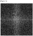
- Figure 1 is a SEM photograph of a polymer membrane formed in the above manner.
- the image of Figure 1 was Fourier-transformed using image analysis software (US National Institute of Health [NIH] open source, "Image J”).
- Figure 2 is the Fourier-transformed image of the polymer membrane.
- Figure 3 is an image obtained by blurring the image of Figure 1 using image analysis software (US National Institute of Health [NIH] open source, "Image J")
- Figure 4 is an image Fourier-transforming the blurring-processed Figure 3 using the same program.
- Figure 5 The image of Figure 5 was subjected to radial integration in the range of 0° to 360° using image analysis software (US National Institute of Health [NIH] open source, "Image J").
- Figure 6 shows the integration result, where as a result of measuring the X coordinate of the first main peak formed in the frequency region of Figure 6 with Image J, the actual region pitch 26.4 nm was measured. This means the pitch of the vertically oriented lamellar structure formed by the self-assembled structure of the polymer membrane formed inside the trench.
- a coating solution prepared by diluting a block copolymer of a compound (DPMC12) and pentafluorostyrene in toluene in a solid content concentration of 1.5 wt% was spin-coated inside the trenches manufactured by the method mentioned in Example 1, dried at room temperature for about 1 hour and then again subjected to the thermal annealing at a temperature of about 160 to 250°C for about 1 hour to form a self-assembled membrane.
- Figure 8 is a SEM photograph of a polymer membrane formed in the above manner.
- the image of Figure 8 was Fourier-transformed using image analysis software (US National Institute of Health [NIH] open source, "Image J”).
- Figure 9 is the Fourier-transformed image of the polymer membrane.
- Figure 10 is an image obtained by blurring the image of Figure 8 using image analysis software (US National Institute of Health [NIH] open source, "Image J")
- Figure 11 is an image Fourier-transforming the blurring-processed Figure 10 using the same program.
- Figure 12 The image of Figure 12 was subjected to radial integration in the range of 0° to 360° using image analysis software (US National Institute of Health [NIH] open source, "Image J").
- Figure 13 shows the integration result, where as a result of measuring the X coordinate of the first main peak formed in the frequency region of Figure 13 with Image J, the actual region pitch 27.8 nm was measured. This means the pitch of the vertically oriented lamellar structure formed by the self-assembled structure of the polymer membrane formed inside the trench.
Description
- The present application relates to a method for analyzing a polymer membrane.
- Block copolymers in which two or more chemically distinct polymer chains are linked by covalent bonds can be separated into regular microphases due to their self assembly characteristics. The microphase separation phenomenon of such a block copolymer is generally explained by volume fractions, molecular weights and mutual attraction coefficients (Flory-Huggins interaction parameter) between constituents, and it may form various structures with nano-scale spheres, cylinders, gyroids or lamellae, and the like.
- An important issue in practical applications of various nanostructures formed by the block copolymers is to control orientation of microphases of the block copolymer. If the spherical block copolymer nanostructure is a zero-dimensional structure having no direction of special orientation, the cylindrical or lamellar nanostructure has orientation as one-dimensional and two-dimensional structures, respectively. Typical orientation properties of the block copolymer may include a parallel orientation in which the orientation of the nanostructure is parallel to the substrate direction and a vertical orientation in which the orientation of the nanostructure is vertical to the substrate direction, where the vertical orientation often has greater importance than the parallel orientation.
- Typically, the orientation of the nanostructure in the membrane of the block copolymer can be determined by whether any one of the blocks of the block copolymer is exposed to the surface or air. That is, the orientation of the nanostructure can be determined by selective wetting of the relevant block, where since a plurality of substrates is generally polar and air is non-polar, a block having a larger polarity in a block copolymer is wetted on a substrate and a block with a smaller polarity is wetted at the interface with air, whereby the parallel orientation is induced.
- Welander et al. investigated constraints on the quality of topographic features needed for graphoepitaxial assembly of cylinder forming poly(styrene-b-methyl methacrylate) (PS-b-PMMA) thin films, showing the impact of trench width roughness (TWR) on feature size uniformity and defect formation. They report that the commensurability between the natural length scale of the block copolymer and the trench width had a significant effect on defectivity, whereas TWR did not play a dominant role (J. Vac. Sci. Technol. B, 2008, 26(6), pp. 2484-2488).
-
JP 2013/200298 A - In order to utilize a self-assembled structure of a block copolymer efficiently, it should be possible to first accurately analyze the structure formed by the block copolymer. However, when the structure of the block copolymer is analyzed by imaging, errors due to noise or the like may occur. Particularly, when the block copolymer is aligned in trenches using graphoepitaxy, the line structures of the trenches and the block copolymer are aligned in the same direction, so that there is a problem that many errors occur in the image analysis of the block copolymer structure.
- In this specification, the term "image" may mean visual information recognizable by human vision, which is reproduced and displayed on a two-dimensional or three-dimensional screen, and may mean various visual information such as still images and videos. The still image or video may be one obtained by using an optical sensor, such as a charge-coupled device (CCD), which is a semiconductor element and digitally acquiring an image coming from a subject to the sensor, and may comprise an image or the like obtained by visually transforming the result value measured using an electron microscope or other measurement equipment. In addition, the "original image" may mean an image itself obtained from the sensor or the like, and may mean an image in which no separate post-processing is performed.
- In this specification, the "Fourier transformation" means to transform pixel values of an image into values in a frequency domain. The Fourier transformation is a widely used technique in signal processing, which is based on the concept that one signal can be represented by synthesis of several sinusoidal signals and can analyze low frequency and high frequency components existing in the image.
- In this specification, the "transformation" may mean changing a format of data according to the designated algorithm. The transformation may mean changing the position, size or property by moving any subject to another position, enlarging, reducing or rotating it, or by expressing it by changing it from one coordinate system to another coordinate system, which may be, for example, a concept including Fourier transformation, image blurring, and the like.
- The image, transformation, Fourier transformation, and the like can be performed using a known numerical analysis program or image processing program, and the like, and the post-processing can be performed to the image using, for example, an image analysis software (US National Institute of Health [NIH] open source, "Image J" or MathWorks, Inc., "MATLAB"), and the like.
- The present application relates to a method for analyzing a polymer membrane according to claim 1. The analysis method of the present application comprises a step of blurring an original image of a polymer membrane having a block copolymer which is formed in trenches disposed at regular intervals and self-assembled. The method of obtaining the image of the polymer membrane is not particularly limited, where the image of the polymer membrane may be digitally acquired using an optical sensor, or may be acquired by visually transforming the result value measured using an electron microscope or other measurement equipment, and the image may be obtained, for example, through a scanning electron microscope (SEM), an atomic force microscope (AFM), or a transmission electron microscope (TEM).
- The method of blurring the obtained image is not particularly limited, which can be performed by a known method. The blurring processing may mean a method of blurring the part which is an outline of the digital image by removing high frequency components (those having a large change rate of pixel values) of the digital image or removing extreme values from the pixel values and assigning the result value that is averaged with neighboring pixels. The blurring processing can use various known blur methods without limitation as long as it can give a blur effect to an image, and for example, a method such as low pass filtering, Gaussian blur, motion blur or radial blur can be used. By performing the blurring processing on the image of the polymer membrane to separate the region corresponding to the trenches and the region corresponding to the self-assembled block copolymer from the original image of the polymer membrane, accurate analysis of the image of the polymer membrane can be allowed. As the method of blurring an image, a known image processing program or the like can be used, and for example, the Fourier transformation can be performed on the obtained image using an image analysis software (US National Institute of Health [NIH] open source, "Image J" or MathWorks, Inc., "MATLAB"), and the like.
- The method further comprises a step of Fourier-transforming the obtained original image and the blurred image. The method of performing the Fourier transformation on the obtained original image and the blurred image is not particularly limited, which can be performed by a known method. As the method of Fourier-transforming an image, a known image processing program or the like can be used, and for example, the Fourier transformation can be performed on the obtained image using an image analysis software (US National Institute of Health [NIH] open source, "Image J" or MathWorks, Inc., "MATLAB"), and the like.
- When the Fourier transformation is performed on the obtained image, the Fourier-transformed image can be obtained. The Fourier-transformed image shows the result that the pixel values of the image are transformed into frequency domain values. Generally, the low frequency region of the Fourier-transformed image represents information on the overall brightness of the image, and the high frequency region represents information on the edge or noise of the image. Through the Fourier transformation, only the information about the noise components included in the image of the polymer membrane can be separated and removed, thereby reducing errors upon analyzing the polymer membrane. By Fourier-transforming the blurred image, it is possible to clarify the difference between the part where the polymer membrane is formed on the substrate and the part where the polymer membrane is not formed thereon, whereby in the analysis of the polymer membrane, the analysis only on the part where the polymer membrane is formed can be allowed.
- The method for analyzing a polymer membrane according to the present application further comprises a step of removing noise from the image generated by the Fourier transformation. Noise is removed from the Fourier-transformed image, thereby reducing errors upon analyzing the polymer membrane. The step of removing noise is a step of removing the overlapping range of the Fourier transformation result of the original image and the Fourier transformation result of the blurred image. By removing the range overlapped with the result of Fourier-transforming the image subjected to the Fourier-transformation after blurring processing from the result of Fourier-transforming the original image, only the region corresponding to the noise other than the polymer membrane can be removed and only the region on the information of the polymer membrane can be acquired. The method of removing the range overlapped with the result of Fourier-transforming the image subjected to the Fourier-transformation after blurring processing from the result of Fourier-transforming the original image is not particularly limited, which can be performed, for example, using a known image analysis software or the like.
- The method for analyzing a polymer membrane of the present application may comprise a step of measuring the pitch of the pattern formed on the surface of the polymer membrane from the Fourier-transformed result of the noise-removed original image. The pattern may mean a shape formed due to a self-assembled structure of a block copolymer to be described below, and may mean a pattern including two or more lines. By measuring the pitch of the pattern from the Fourier-transformed image, it is possible to accurately analyze the self-assembled structure of the polymer membrane.
- In one example of the present application, the pitch of the pattern formed on the surface of the polymer membrane can be measured by converting a two-dimensional spectral image formed by Fourier transformation into a one-dimensional graph through radial integration. Specifically, the step of measuring a pitch is a step of measuring a peak formed by radially integrating the Fourier-transformed image of the polymer membrane in the range of 0° to 360°. If the Fourier-transformed two-dimensional image is radially integrated in the range of 0° to 360°, the one-dimensional graph expressing the density of frequency can be obtained, where the X coordinate value of the first peak on the frequency domain graph may mean the pitch of the actual region of the pattern formed on the surface of the polymer membrane. By measuring the pitch of the pattern formed on the surface of the polymer membrane using the peak value, it is possible to accurately analyze the structure of the polymer membrane.
- The polymer membrane of the present application may be formed on a substrate on which trenches are formed. The type of the substrate applied to the method of the present application is not particularly limited. As the substrate, for example, various types of substrates requiring formation of a pattern on the surface may all be used for applying each of the above-described applications. A substrate of this type may include a semiconductor substrate such as a silicon substrate, a silicon germanium substrate, a GaAs substrate and a silicon oxide substrate. As the substrate, for example, a substrate may be used, which is applied to form finFETs (fin field effect transistors) or other electronic devices such as diodes, transistors or capacitors. In addition, other materials such as ceramics may be used as the substrate depending on applications, and the types of substrates that can be applied in the present application are not limited thereto.
- Mesa structures may be formed on the surface of the substrate applied to the method of the present application from each other at intervals, and trenches may be formed by the mesa structures. For example, the mesa structures may each be in the form of a line. Such mesa structures may be spaced apart from each other at regular intervals and disposed on the substrate surface. The mesa structures may be disposed substantially parallel to one another on the surface of the substrate. At least two or more mesa structures may be formed on the surface of the substrate. That is, the number of trenches formed by the mesa structures on the surface of the substrate may be one or more. The number of the mesa structures and the trenches is not particularly limited, which may be adjusted depending on applications.
- The ratio (D/H) of the distance (D) of the mesa structures spaced apart to form the trench to the height (H) of the mesa structure is not particularly limited, which may be, for example, 0.1 or more and may be 10 or less. In addition, the ratio (D/W) of the distance (D) between the mesa structures to the width (W) of the mesa structure is not particularly limited, which may be 0.5 or more and may be 10 or less. The ratio (D/H or D/W) may be changed according to the intended use. In this specification, the term distance (D) of mesa structures means the shortest distance between adjacent mesa structures spaced apart, where the distance (D) may be, for example, 5 nm or more and may be 500 nm or less. In this specification, the term height (H) of mesa structure is a dimension of a mesa structure measured in the upward direction along the normal direction of the substrate surface based on the surface of the substrate, which may be, for example, 1 nm or more and may be 100 nm or less. In this specification, the term width (W) of mesa structure is a dimension of a mesa structure measured along the direction vertical to the normal direction of the substrate surface, which may be, for example, 5 nm or more and may be 500 nm or less. For example, when the block copolymer is applied as the inductive self-assembly material and the lamella pattern of the block copolymer is formed, the distance of mesa structures may be in a range of about 1L to 20L. In this case, the membrane comprising the block copolymer, i.e. the membrane formed in the trenches, may have a thickness in the range of about 0.1L to 10L or 1L to 8L. The dimension or the like of the mesa structure is one example of the present application, which can be changed according to a specific aspect.
- A method of forming such mesa structures on a substrate is not particularly limited, where a known method can be applied. For example, the mesa structures can be formed by etching the substrate in an appropriate manner, or by depositing an appropriate material on the substrate.
- Here, the kind of the mesa structure forming material is not particularly limited. For example, as the material, a material capable of being etched by an etching process to form a mesa structure may be used. For example, as the material, SiO2, ACL (amorphous carbon layer), SOG (spin-on-glass), SOC (spin-on-carbon) or silicon nitride, and the like may be applied. The layer of such a material may be coated by a method such as spin coating or may be formed by a vapor deposition method such as CVD (chemical vapor deposition). When the layer of the material is formed, its thickness or the like is not particularly limited, and the layer may be formed to have an appropriate thickness in consideration of the height (H) of the desired mesa structure.
- In the present application, the polymer membrane comprises a block copolymer. The block copolymer may be a block copolymer having a first block and a second block chemically distinct from the first block. The block copolymer may mean a molecular structure in which polymer blocks having different chemical structures are linked through covalent bonds.
- The block copolymer may form a self-assembled structure. The self-assembled structure may mean that a specific structure is formed by interaction between the respective blocks included in the block copolymer. The self-assembled structure of the block copolymer may be a sphere, cylinder or lamella structure. In one example, the block copolymer may be present in a vertically oriented state in the case of the sphere or lamellar of the structures. For example, within the segments of the first or second block or other blocks covalently bonded thereto in the block copolymer, the other segments may be vertically oriented, while forming a regular structure such as a lamellar shape or a cylinder shape. The block copolymer that can be included in the polymer membrane of the present application is not particularly limited.
- The block copolymer of the present application may be a diblock copolymer comprising the first block and the second block as described above, or may be a multi-block copolymer that comprises one or more of the first block and the second block by two or more, or comprises a different type of third block.
- The method of forming such a polymer membrane using a block copolymer is not particularly limited. For example, the method of forming a polymer membrane may comprise a process of forming a layer of the block copolymer or a coating solution obtained by diluting it in an appropriate solvent on a neutral layer by coating or the like, and if necessary, aging or heat-treating the layer.
- The aging or heat treatment may be performed based on, for example, the phase transition temperature or the glass transition temperature of the block copolymer, and may be performed at, for example, a temperature above the glass transition temperature or the phase transition temperature. The time for which this heat treatment is performed is not particularly limited, and it can be performed in a range of, for example, about 1 minute to 72 hours, but this can be changed as required. In addition, the heat treatment temperature of the polymer thin membrane may be, for example, 100°C to 250°C or so, but this may be changed in consideration of the block copolymer to be used. In another example, the formed layer may also be solvent-aged for about 1 minute to 72 hours in a non-polar solvent and/or a polar solvent at room temperature.
- The method for analyzing a polymer membrane of the present application can improve accuracy of structural analysis of the polymer membrane and shorten the analysis time by effectively removing noise.
-
-
Figure 1 is an SEM photograph of a polymer membrane including a block copolymer formed in trenches. -
Figure 2 is an image Fourier-transforming the image ofFigure 1 . -
Figure 3 is an image obtained by performing blurring processing on the image ofFigure 1 . -
Figure 4 is an image Fourier-transforming the image ofFigure 3 . -
Figure 5 is an image removing the region overlapping withFigure 4 fromFigure 2 . -
Figure 6 is the result of integrating the image ofFigure 5 . -
Figure 7 is the result of integrating the image ofFigure 2 . -
Figure 8 is a SEM photograph of a polymer membrane including a block copolymer formed in trenches. -
Figure 9 is an image Fourier-transforming the image ofFigure 8 . -
Figure 10 is an image obtained by performing blurring processing on the image ofFigure 8 . -
Figure 11 is an image Fourier-transforming the image ofFigure 10 . -
Figure 12 is an image removing the region overlapping withFigure 11 fromFigure 9 . -
Figure 13 is the result of integrating the image ofFigure 12 . -
Figure 14 is the result of integrating the image ofFigure 9 . - Hereinafter, the present application will be described more in detail by way of examples according to the present application and comparative examples, but the scope of the present application is not limited by the following examples.
- A trench substrate was prepared in the following manner. A silicon wafer was applied as a substrate. A layer of SiO was formed on the substrate to a thickness of about 200 nm or so by a known deposition method. Subsequently, a BARC (bottom anti-reflective coating) was coated on the layer of SiO to a thickness of about 60 nm or so, and a PR (photoresist, for KrF, positive-tone resist) layer was again coated thereon to a thickness of about 400 nm or so. Subsequently, the PR layer was patterned by a KrF stepper exposure method. Subsequently, using the patterned PR layer as a mask, the lower BARC layer and SiO layer were etched by an RIE (reactive ion etching) method, and the residue was removed to form a trench structure.
- A random copolymer of a compound (DPM-C12) and pentafluorostyrene was coated inside the trenches and fixed on the silicon wafer through a thermal annealing process at 160°C for 24 hours, and to remove unreacted materials, a sonication process was treated on a fluorobenzene solution for 10 minutes. A coating solution prepared by diluting a block copolymer of a compound (DPM-C12) of Formula A below and pentafluorostyrene in toluene in a solid content concentration of 1.5 wt% was spin-coated inside the trenches, dried at room temperature for about 1 hour and then again subjected to the thermal annealing at a temperature of about 160 to 250°C for about 1 hour to form a self-assembled membrane.

- In Formula A, R is a linear alkyl group having 12 carbon atoms.
-
Figure 1 is a SEM photograph of a polymer membrane formed in the above manner. The image ofFigure 1 was Fourier-transformed using image analysis software (US National Institute of Health [NIH] open source, "Image J").Figure 2 is the Fourier-transformed image of the polymer membrane. - Furthermore,
Figure 3 is an image obtained by blurring the image ofFigure 1 using image analysis software (US National Institute of Health [NIH] open source, "Image J"), andFigure 4 is an image Fourier-transforming the blurring-processedFigure 3 using the same program. - The region overlapping with
Figure 4 was removed from the image ofFigure 2 , whereFigure 5 is the image ofFigure 2 after removing the region overlapping withFigure 4 . - The image of
Figure 5 was subjected to radial integration in the range of 0° to 360° using image analysis software (US National Institute of Health [NIH] open source, "Image J").Figure 6 shows the integration result, where as a result of measuring the X coordinate of the first main peak formed in the frequency region ofFigure 6 with Image J, the actual region pitch 26.4 nm was measured. This means the pitch of the vertically oriented lamellar structure formed by the self-assembled structure of the polymer membrane formed inside the trench. - A coating solution prepared by diluting a block copolymer of a compound (DPMC12) and pentafluorostyrene in toluene in a solid content concentration of 1.5 wt% was spin-coated inside the trenches manufactured by the method mentioned in Example 1, dried at room temperature for about 1 hour and then again subjected to the thermal annealing at a temperature of about 160 to 250°C for about 1 hour to form a self-assembled membrane.
-
Figure 8 is a SEM photograph of a polymer membrane formed in the above manner. The image ofFigure 8 was Fourier-transformed using image analysis software (US National Institute of Health [NIH] open source, "Image J").Figure 9 is the Fourier-transformed image of the polymer membrane. - Furthermore,
Figure 10 is an image obtained by blurring the image ofFigure 8 using image analysis software (US National Institute of Health [NIH] open source, "Image J"), andFigure 11 is an image Fourier-transforming the blurring-processedFigure 10 using the same program. - The region overlapping with
Figure 11 was removed from the image ofFigure 9 , whereFigure 12 is the image ofFigure 9 after removing the region overlapping withFigure 11 . - The image of
Figure 12 was subjected to radial integration in the range of 0° to 360° using image analysis software (US National Institute of Health [NIH] open source, "Image J").Figure 13 shows the integration result, where as a result of measuring the X coordinate of the first main peak formed in the frequency region ofFigure 13 with Image J, the actual region pitch 27.8 nm was measured. This means the pitch of the vertically oriented lamellar structure formed by the self-assembled structure of the polymer membrane formed inside the trench. - The experiment was performed under the same conditions as in Example 1, except that the image of
Figure 1 was not subjected to the blurring processing and the integration of the Fourier-transformed image ofFigure 2 was performed.Figure 7 shows the result of performing the radial integration in the range of 0° to 360° using image analysis software (US National Institute of Health [NIH] open source, "Image J") on the image ofFigure 2 . As could be seen fromFigure 7 , no peak was formed as a result of transforming the image without blurring processing. This is due to the noise generated because the trench structure formed on the substrate and the vertically oriented lamellar structure formed by the self-assembled structure of the block copolymer are aligned in the same direction, which shows the result that the pitch of the vertically oriented lamellar structure cannot be calculated. - The experiment was performed under the same conditions as in Example 2, except that the image of
Figure 8 was not subjected to the blurring processing and the integration of the Fourier-transformed image ofFigure 9 was performed.Figure 14 shows the result of performing the radial integration in the range of 0° to 360° using image analysis software (US National Institute of Health [NIH] open source, "Image J") on the image ofFigure 9 . As could be seen fromFigure 14 , no peak was formed as a result of transforming the image without blurring processing. This is due to the noise generated because the trench structure formed on the substrate and the vertically oriented lamellar structure formed by the self-assembled structure of the block copolymer are aligned in the same direction, which shows the result that the pitch of the vertically oriented lamellar structure cannot be calculated.
Claims (5)
- A method for analyzing a polymer membrane having a block copolymer which is formed in trenches disposed at regular intervals and self-assembled, the method comprising:a step of blurring an original image of the polymer membrane, characterized in that the step of blurring the original image of the polymer membrane is to separate the region corresponding to the trenches and the region corresponding to the self-assembled block copolymer from the original image of the polymer membrane,and characterized in that the method further comprises:a step of Fourier-transforming the original image and the blurring-processed image, anda step of removing noise from the image generated by the Fourier transformation of the original image,wherein the step of removing noise is a step of removing the overlapping range of the Fourier transformation result of the original image and the Fourier transformation result of the blurring-processed image.
- The method for analyzing a polymer membrane according to claim 1, further comprising a step of measuring a pitch of a pattern formed on the surface of the polymer membrane from the Fourier-transformed result of the noise-removed original image.
- The method for analyzing a polymer membrane according to claim 2, wherein the step of measuring a pitch is a step of measuring a peak formed by radially integrating the Fourier-transformed image of the polymer membrane in the range of 0° to 360°.
- The method for analyzing a polymer membrane according to claim 1, wherein the self-assembled structure of the block copolymer is a cylinder, sphere or lamellar structure.
- The method for analyzing a polymer membrane according to claim 1, wherein the original image of the polymer membrane is an image obtained through a scanning electron microscope (SEM), an atomic force microscope (AFM) or a transmission electron microscope (TEM).
Applications Claiming Priority (2)
| Application Number | Priority Date | Filing Date | Title |
|---|---|---|---|
| KR1020170089864A KR102176230B1 (en) | 2017-07-14 | 2017-07-14 | Method for analyzing polymer layer |
| PCT/KR2018/008019 WO2019013603A1 (en) | 2017-07-14 | 2018-07-16 | Method for analyzing polymer layer |
Publications (3)
| Publication Number | Publication Date |
|---|---|
| EP3637366A1 EP3637366A1 (en) | 2020-04-15 |
| EP3637366A4 EP3637366A4 (en) | 2020-07-08 |
| EP3637366B1 true EP3637366B1 (en) | 2022-05-25 |
Family
ID=65002619
Family Applications (1)
| Application Number | Title | Priority Date | Filing Date |
|---|---|---|---|
| EP18832906.4A Active EP3637366B1 (en) | 2017-07-14 | 2018-07-16 | Method for analyzing polymer layer |
Country Status (6)
| Country | Link |
|---|---|
| US (1) | US11145049B2 (en) |
| EP (1) | EP3637366B1 (en) |
| JP (1) | JP6874948B2 (en) |
| KR (1) | KR102176230B1 (en) |
| CN (1) | CN110785665B (en) |
| WO (1) | WO2019013603A1 (en) |
Family Cites Families (20)
| Publication number | Priority date | Publication date | Assignee | Title |
|---|---|---|---|---|
| TW463282B (en) * | 2000-11-03 | 2001-11-11 | Promos Technologies Inc | Integrated circuit defect inspection using Fourier transform spatial filtering technique |
| JP3586431B2 (en) * | 2001-02-28 | 2004-11-10 | 松下電器産業株式会社 | Personal authentication method and device |
| JP3794361B2 (en) * | 2002-08-28 | 2006-07-05 | 三菱電機株式会社 | Radar signal processing apparatus and radar signal processing method |
| JP2004233163A (en) | 2003-01-29 | 2004-08-19 | Hitachi High-Technologies Corp | Method and device for inspecting pattern defect |
| JP3837543B2 (en) | 2003-04-24 | 2006-10-25 | 独立行政法人産業技術総合研究所 | Analytical method and analytical apparatus for polymer |
| WO2005114338A1 (en) * | 2004-05-20 | 2005-12-01 | Mcmaster University | Method for controlling the appearance of products and process performance by image analysis |
| US7437012B2 (en) * | 2004-05-27 | 2008-10-14 | United States Of America As Represented By The Secretary Of Commerce, The National Institute Of Standards & Technology | Singular integral image deblurring method |
| JP2006106243A (en) * | 2004-10-04 | 2006-04-20 | Nitto Denko Corp | Forming method of regular two dimensional periodic structure section on photosensitive high polymer film surface |
| US7970239B2 (en) * | 2006-01-19 | 2011-06-28 | Qualcomm Incorporated | Hand jitter reduction compensating for rotational motion |
| KR101120966B1 (en) | 2006-09-25 | 2012-03-05 | 퀄컴 인코포레이티드 | A hand jitter reduction system for cameras |
| KR100958962B1 (en) * | 2007-12-31 | 2010-05-20 | 주식회사 포스코아이씨티 | Apparatus and Method of fingerprint classification |
| JP5178558B2 (en) | 2009-02-03 | 2013-04-10 | 株式会社日立ハイテクノロジーズ | Method for adjusting optical axis of charged particle beam and charged particle beam apparatus |
| JP2013200298A (en) * | 2012-02-23 | 2013-10-03 | Toray Ind Inc | Dispersion property evaluation method of island part in resin composition, and dispersion property evaluation device of island part in resin composition |
| JP5957357B2 (en) | 2012-10-15 | 2016-07-27 | 株式会社日立ハイテクノロジーズ | Pattern inspection / measurement apparatus and program |
| KR101359206B1 (en) * | 2013-01-18 | 2014-02-07 | 연세대학교 산학협력단 | Method and apparatus for eliminating noise in magnetic resonance images |
| US20150022658A1 (en) * | 2013-07-16 | 2015-01-22 | University Of North Carolina At Charlotte | Noise reduction techniques, fractional bi-spectrum and fractional cross-correlation, and applications |
| CN105899557B (en) | 2013-12-06 | 2018-10-26 | 株式会社Lg化学 | Block copolymer |
| EP3029178A1 (en) | 2014-12-05 | 2016-06-08 | ATOTECH Deutschland GmbH | Method and apparatus for electroplating a metal onto a substrate |
| CN105261006B (en) * | 2015-09-11 | 2017-12-19 | 浙江工商大学 | Medical image segmentation algorithm based on Fourier transformation |
| KR101767564B1 (en) | 2015-11-12 | 2017-08-11 | 성균관대학교산학협력단 | A method of analysing images of rod-like particles |
-
2017
- 2017-07-14 KR KR1020170089864A patent/KR102176230B1/en active IP Right Grant
-
2018
- 2018-07-16 CN CN201880042248.0A patent/CN110785665B/en active Active
- 2018-07-16 EP EP18832906.4A patent/EP3637366B1/en active Active
- 2018-07-16 US US16/629,858 patent/US11145049B2/en active Active
- 2018-07-16 JP JP2019571710A patent/JP6874948B2/en active Active
- 2018-07-16 WO PCT/KR2018/008019 patent/WO2019013603A1/en unknown
Also Published As
| Publication number | Publication date |
|---|---|
| CN110785665B (en) | 2022-05-10 |
| US20200402224A1 (en) | 2020-12-24 |
| KR20190008025A (en) | 2019-01-23 |
| JP2020527781A (en) | 2020-09-10 |
| US11145049B2 (en) | 2021-10-12 |
| WO2019013603A1 (en) | 2019-01-17 |
| JP6874948B2 (en) | 2021-05-19 |
| EP3637366A1 (en) | 2020-04-15 |
| EP3637366A4 (en) | 2020-07-08 |
| CN110785665A (en) | 2020-02-11 |
| KR102176230B1 (en) | 2020-11-09 |
Similar Documents
| Publication | Publication Date | Title |
|---|---|---|
| Murphy et al. | Automated defect and correlation length analysis of block copolymer thin film nanopatterns | |
| US8551566B2 (en) | Directed material assembly | |
| Tiron et al. | Optimization of block copolymer self-assembly through graphoepitaxy: a defectivity study | |
| Tu et al. | Universal pattern transfer methods for metal nanostructures by block copolymer lithography | |
| US20130140272A1 (en) | Lithography using self-assembled polymers | |
| EP2845887B1 (en) | Process for controlling the period of a nanostructured assemblage comprising a blend of block copolymers | |
| US9367910B2 (en) | Self-assemblable polymer and methods for use in lithography | |
| EP3637366B1 (en) | Method for analyzing polymer layer | |
| Gronheid et al. | Readying directed self-assembly for patterning in semi-conductor manufacturing | |
| Ghoshal et al. | Development of a facile block copolymer method for creating hard mask patterns integrated into semiconductor manufacturing | |
| KR102171206B1 (en) | Method for quantitative measurement of defects within block-copolymer thin-flim having lamellar pattern | |
| EP3308955A1 (en) | Laminate | |
| Borah et al. | Nanoscale silicon substrate patterns from self-assembly of cylinder forming poly (styrene)-block-poly (dimethylsiloxane) block copolymer on silane functionalized surfaces | |
| Kihara et al. | Sub-10-nm patterning process using directed self-assembly with high χ block copolymers | |
| Doise et al. | Defect mitigation in sub-20nm patterning with high-chi, silicon-containing block copolymers | |
| Blachut et al. | Evolution of roughness during the pattern transfer of high-chi, 10nm half-pitch, silicon-containing block copolymer structures | |
| Zhou et al. | Studying the effects of chemistry and geometry on DSA hole-shrink process in three-dimensions | |
| Wang et al. | Double layer lift-off nanofabrication controlled gaps of nanoelectrodes with sub-100 nm by nanoimprint lithography | |
| Raczkowska et al. | Pattern replication examined with integral geometry approach: application to ion milling of polymer blend films | |
| US20170287126A1 (en) | Method of evaluating aligned patterns in directed self-assembly and using in feedback control scheme | |
| KR101030457B1 (en) | Method for detecting align mark using invariant moment and Apparatus thereof | |
| KR102425189B1 (en) | Method for analyzing polymer layer | |
| KR102171207B1 (en) | Method for quantitative measurement of defects within block-copolymer thin-flim having lamellar pattern | |
| Higo et al. | High Throughput 16 NM Nanogap by Variable Shaped Beam Method Using F7000S-VD02 EB Lithography | |
| Li | Directed Assembly of Functional Nanomaterials Using Chemical Patterns |
Legal Events
| Date | Code | Title | Description |
|---|---|---|---|
| STAA | Information on the status of an ep patent application or granted ep patent |
Free format text: STATUS: THE INTERNATIONAL PUBLICATION HAS BEEN MADE |
|
| PUAI | Public reference made under article 153(3) epc to a published international application that has entered the european phase |
Free format text: ORIGINAL CODE: 0009012 |
|
| STAA | Information on the status of an ep patent application or granted ep patent |
Free format text: STATUS: REQUEST FOR EXAMINATION WAS MADE |
|
| 17P | Request for examination filed |
Effective date: 20200110 |
|
| AK | Designated contracting states |
Kind code of ref document: A1 Designated state(s): AL AT BE BG CH CY CZ DE DK EE ES FI FR GB GR HR HU IE IS IT LI LT LU LV MC MK MT NL NO PL PT RO RS SE SI SK SM TR |
|
| AX | Request for extension of the european patent |
Extension state: BA ME |
|
| A4 | Supplementary search report drawn up and despatched |
Effective date: 20200608 |
|
| RIC1 | Information provided on ipc code assigned before grant |
Ipc: G06T 5/00 20060101ALI20200602BHEP Ipc: C08J 5/22 20060101ALI20200602BHEP Ipc: G01N 33/44 20060101ALI20200602BHEP Ipc: G06T 7/00 20170101AFI20200602BHEP Ipc: C08L 53/00 20060101ALI20200602BHEP Ipc: G06T 7/60 20170101ALI20200602BHEP Ipc: G06K 9/40 20060101ALI20200602BHEP Ipc: C09D 153/00 20060101ALI20200602BHEP Ipc: G01N 21/17 20060101ALI20200602BHEP Ipc: G01Q 30/02 20100101ALI20200602BHEP Ipc: G06T 5/50 20060101ALI20200602BHEP |
|
| DAV | Request for validation of the european patent (deleted) | ||
| DAX | Request for extension of the european patent (deleted) | ||
| GRAP | Despatch of communication of intention to grant a patent |
Free format text: ORIGINAL CODE: EPIDOSNIGR1 |
|
| STAA | Information on the status of an ep patent application or granted ep patent |
Free format text: STATUS: GRANT OF PATENT IS INTENDED |
|
| RIC1 | Information provided on ipc code assigned before grant |
Ipc: G06K 9/52 20060101ALI20211201BHEP Ipc: G06K 9/00 20060101ALI20211201BHEP Ipc: G06T 5/50 20060101ALI20211201BHEP Ipc: G06T 5/00 20060101ALI20211201BHEP Ipc: G01N 33/44 20060101ALI20211201BHEP Ipc: G01N 21/17 20060101ALI20211201BHEP Ipc: C09D 153/00 20060101ALI20211201BHEP Ipc: G06K 9/40 20060101ALI20211201BHEP Ipc: G06T 7/60 20170101ALI20211201BHEP Ipc: G06T 7/00 20170101AFI20211201BHEP |
|
| INTG | Intention to grant announced |
Effective date: 20211220 |
|
| GRAS | Grant fee paid |
Free format text: ORIGINAL CODE: EPIDOSNIGR3 |
|
| GRAA | (expected) grant |
Free format text: ORIGINAL CODE: 0009210 |
|
| STAA | Information on the status of an ep patent application or granted ep patent |
Free format text: STATUS: THE PATENT HAS BEEN GRANTED |
|
| AK | Designated contracting states |
Kind code of ref document: B1 Designated state(s): AL AT BE BG CH CY CZ DE DK EE ES FI FR GB GR HR HU IE IS IT LI LT LU LV MC MK MT NL NO PL PT RO RS SE SI SK SM TR |
|
| REG | Reference to a national code |
Ref country code: GB Ref legal event code: FG4D |
|
| REG | Reference to a national code |
Ref country code: CH Ref legal event code: EP |
|
| REG | Reference to a national code |
Ref country code: DE Ref legal event code: R096 Ref document number: 602018036039 Country of ref document: DE |
|
| REG | Reference to a national code |
Ref country code: AT Ref legal event code: REF Ref document number: 1494567 Country of ref document: AT Kind code of ref document: T Effective date: 20220615 |
|
| REG | Reference to a national code |
Ref country code: IE Ref legal event code: FG4D |
|
| REG | Reference to a national code |
Ref country code: LT Ref legal event code: MG9D |
|
| REG | Reference to a national code |
Ref country code: NL Ref legal event code: MP Effective date: 20220525 |
|
| REG | Reference to a national code |
Ref country code: AT Ref legal event code: MK05 Ref document number: 1494567 Country of ref document: AT Kind code of ref document: T Effective date: 20220525 |
|
| PG25 | Lapsed in a contracting state [announced via postgrant information from national office to epo] |
Ref country code: SE Free format text: LAPSE BECAUSE OF FAILURE TO SUBMIT A TRANSLATION OF THE DESCRIPTION OR TO PAY THE FEE WITHIN THE PRESCRIBED TIME-LIMIT Effective date: 20220525 Ref country code: PT Free format text: LAPSE BECAUSE OF FAILURE TO SUBMIT A TRANSLATION OF THE DESCRIPTION OR TO PAY THE FEE WITHIN THE PRESCRIBED TIME-LIMIT Effective date: 20220926 Ref country code: NO Free format text: LAPSE BECAUSE OF FAILURE TO SUBMIT A TRANSLATION OF THE DESCRIPTION OR TO PAY THE FEE WITHIN THE PRESCRIBED TIME-LIMIT Effective date: 20220825 Ref country code: NL Free format text: LAPSE BECAUSE OF FAILURE TO SUBMIT A TRANSLATION OF THE DESCRIPTION OR TO PAY THE FEE WITHIN THE PRESCRIBED TIME-LIMIT Effective date: 20220525 Ref country code: LT Free format text: LAPSE BECAUSE OF FAILURE TO SUBMIT A TRANSLATION OF THE DESCRIPTION OR TO PAY THE FEE WITHIN THE PRESCRIBED TIME-LIMIT Effective date: 20220525 Ref country code: HR Free format text: LAPSE BECAUSE OF FAILURE TO SUBMIT A TRANSLATION OF THE DESCRIPTION OR TO PAY THE FEE WITHIN THE PRESCRIBED TIME-LIMIT Effective date: 20220525 Ref country code: GR Free format text: LAPSE BECAUSE OF FAILURE TO SUBMIT A TRANSLATION OF THE DESCRIPTION OR TO PAY THE FEE WITHIN THE PRESCRIBED TIME-LIMIT Effective date: 20220826 Ref country code: FI Free format text: LAPSE BECAUSE OF FAILURE TO SUBMIT A TRANSLATION OF THE DESCRIPTION OR TO PAY THE FEE WITHIN THE PRESCRIBED TIME-LIMIT Effective date: 20220525 Ref country code: ES Free format text: LAPSE BECAUSE OF FAILURE TO SUBMIT A TRANSLATION OF THE DESCRIPTION OR TO PAY THE FEE WITHIN THE PRESCRIBED TIME-LIMIT Effective date: 20220525 Ref country code: BG Free format text: LAPSE BECAUSE OF FAILURE TO SUBMIT A TRANSLATION OF THE DESCRIPTION OR TO PAY THE FEE WITHIN THE PRESCRIBED TIME-LIMIT Effective date: 20220825 Ref country code: AT Free format text: LAPSE BECAUSE OF FAILURE TO SUBMIT A TRANSLATION OF THE DESCRIPTION OR TO PAY THE FEE WITHIN THE PRESCRIBED TIME-LIMIT Effective date: 20220525 |
|
| PG25 | Lapsed in a contracting state [announced via postgrant information from national office to epo] |
Ref country code: RS Free format text: LAPSE BECAUSE OF FAILURE TO SUBMIT A TRANSLATION OF THE DESCRIPTION OR TO PAY THE FEE WITHIN THE PRESCRIBED TIME-LIMIT Effective date: 20220525 Ref country code: PL Free format text: LAPSE BECAUSE OF FAILURE TO SUBMIT A TRANSLATION OF THE DESCRIPTION OR TO PAY THE FEE WITHIN THE PRESCRIBED TIME-LIMIT Effective date: 20220525 Ref country code: LV Free format text: LAPSE BECAUSE OF FAILURE TO SUBMIT A TRANSLATION OF THE DESCRIPTION OR TO PAY THE FEE WITHIN THE PRESCRIBED TIME-LIMIT Effective date: 20220525 Ref country code: IS Free format text: LAPSE BECAUSE OF FAILURE TO SUBMIT A TRANSLATION OF THE DESCRIPTION OR TO PAY THE FEE WITHIN THE PRESCRIBED TIME-LIMIT Effective date: 20220925 |
|
| PG25 | Lapsed in a contracting state [announced via postgrant information from national office to epo] |
Ref country code: SM Free format text: LAPSE BECAUSE OF FAILURE TO SUBMIT A TRANSLATION OF THE DESCRIPTION OR TO PAY THE FEE WITHIN THE PRESCRIBED TIME-LIMIT Effective date: 20220525 Ref country code: SK Free format text: LAPSE BECAUSE OF FAILURE TO SUBMIT A TRANSLATION OF THE DESCRIPTION OR TO PAY THE FEE WITHIN THE PRESCRIBED TIME-LIMIT Effective date: 20220525 Ref country code: RO Free format text: LAPSE BECAUSE OF FAILURE TO SUBMIT A TRANSLATION OF THE DESCRIPTION OR TO PAY THE FEE WITHIN THE PRESCRIBED TIME-LIMIT Effective date: 20220525 Ref country code: EE Free format text: LAPSE BECAUSE OF FAILURE TO SUBMIT A TRANSLATION OF THE DESCRIPTION OR TO PAY THE FEE WITHIN THE PRESCRIBED TIME-LIMIT Effective date: 20220525 Ref country code: DK Free format text: LAPSE BECAUSE OF FAILURE TO SUBMIT A TRANSLATION OF THE DESCRIPTION OR TO PAY THE FEE WITHIN THE PRESCRIBED TIME-LIMIT Effective date: 20220525 Ref country code: CZ Free format text: LAPSE BECAUSE OF FAILURE TO SUBMIT A TRANSLATION OF THE DESCRIPTION OR TO PAY THE FEE WITHIN THE PRESCRIBED TIME-LIMIT Effective date: 20220525 |
|
| PG25 | Lapsed in a contracting state [announced via postgrant information from national office to epo] |
Ref country code: MC Free format text: LAPSE BECAUSE OF FAILURE TO SUBMIT A TRANSLATION OF THE DESCRIPTION OR TO PAY THE FEE WITHIN THE PRESCRIBED TIME-LIMIT Effective date: 20220525 |
|
| REG | Reference to a national code |
Ref country code: DE Ref legal event code: R097 Ref document number: 602018036039 Country of ref document: DE Ref country code: CH Ref legal event code: PL |
|
| REG | Reference to a national code |
Ref country code: BE Ref legal event code: MM Effective date: 20220731 |
|
| PG25 | Lapsed in a contracting state [announced via postgrant information from national office to epo] |
Ref country code: AL Free format text: LAPSE BECAUSE OF FAILURE TO SUBMIT A TRANSLATION OF THE DESCRIPTION OR TO PAY THE FEE WITHIN THE PRESCRIBED TIME-LIMIT Effective date: 20220525 |
|
| PLBE | No opposition filed within time limit |
Free format text: ORIGINAL CODE: 0009261 |
|
| STAA | Information on the status of an ep patent application or granted ep patent |
Free format text: STATUS: NO OPPOSITION FILED WITHIN TIME LIMIT |
|
| PG25 | Lapsed in a contracting state [announced via postgrant information from national office to epo] |
Ref country code: LU Free format text: LAPSE BECAUSE OF NON-PAYMENT OF DUE FEES Effective date: 20220716 Ref country code: LI Free format text: LAPSE BECAUSE OF NON-PAYMENT OF DUE FEES Effective date: 20220731 Ref country code: CH Free format text: LAPSE BECAUSE OF NON-PAYMENT OF DUE FEES Effective date: 20220731 |
|
| 26N | No opposition filed |
Effective date: 20230228 |
|
| PG25 | Lapsed in a contracting state [announced via postgrant information from national office to epo] |
Ref country code: SI Free format text: LAPSE BECAUSE OF FAILURE TO SUBMIT A TRANSLATION OF THE DESCRIPTION OR TO PAY THE FEE WITHIN THE PRESCRIBED TIME-LIMIT Effective date: 20220525 Ref country code: BE Free format text: LAPSE BECAUSE OF NON-PAYMENT OF DUE FEES Effective date: 20220731 |
|
| PG25 | Lapsed in a contracting state [announced via postgrant information from national office to epo] |
Ref country code: IE Free format text: LAPSE BECAUSE OF NON-PAYMENT OF DUE FEES Effective date: 20220716 |
|
| PGFP | Annual fee paid to national office [announced via postgrant information from national office to epo] |
Ref country code: FR Payment date: 20230621 Year of fee payment: 6 |
|
| PGFP | Annual fee paid to national office [announced via postgrant information from national office to epo] |
Ref country code: GB Payment date: 20230620 Year of fee payment: 6 |
|
| PGFP | Annual fee paid to national office [announced via postgrant information from national office to epo] |
Ref country code: DE Payment date: 20230620 Year of fee payment: 6 |
|
| PG25 | Lapsed in a contracting state [announced via postgrant information from national office to epo] |
Ref country code: IT Free format text: LAPSE BECAUSE OF FAILURE TO SUBMIT A TRANSLATION OF THE DESCRIPTION OR TO PAY THE FEE WITHIN THE PRESCRIBED TIME-LIMIT Effective date: 20220525 |
|
| PG25 | Lapsed in a contracting state [announced via postgrant information from national office to epo] |
Ref country code: HU Free format text: LAPSE BECAUSE OF FAILURE TO SUBMIT A TRANSLATION OF THE DESCRIPTION OR TO PAY THE FEE WITHIN THE PRESCRIBED TIME-LIMIT; INVALID AB INITIO Effective date: 20180716 |
|
| PG25 | Lapsed in a contracting state [announced via postgrant information from national office to epo] |
Ref country code: MK Free format text: LAPSE BECAUSE OF FAILURE TO SUBMIT A TRANSLATION OF THE DESCRIPTION OR TO PAY THE FEE WITHIN THE PRESCRIBED TIME-LIMIT Effective date: 20220525 Ref country code: CY Free format text: LAPSE BECAUSE OF FAILURE TO SUBMIT A TRANSLATION OF THE DESCRIPTION OR TO PAY THE FEE WITHIN THE PRESCRIBED TIME-LIMIT Effective date: 20220525 |