EP3637324A1 - Geometric constellation shaping for optical data transport - Google Patents
Geometric constellation shaping for optical data transport Download PDFInfo
- Publication number
- EP3637324A1 EP3637324A1 EP18199135.7A EP18199135A EP3637324A1 EP 3637324 A1 EP3637324 A1 EP 3637324A1 EP 18199135 A EP18199135 A EP 18199135A EP 3637324 A1 EP3637324 A1 EP 3637324A1
- Authority
- EP
- European Patent Office
- Prior art keywords
- stream
- bit
- optical
- digital
- artificial neural
- Prior art date
- Legal status (The legal status is an assumption and is not a legal conclusion. Google has not performed a legal analysis and makes no representation as to the accuracy of the status listed.)
- Pending
Links
Images



Classifications
-
- H—ELECTRICITY
- H04—ELECTRIC COMMUNICATION TECHNIQUE
- H04Q—SELECTING
- H04Q11/00—Selecting arrangements for multiplex systems
- H04Q11/0001—Selecting arrangements for multiplex systems using optical switching
- H04Q11/0062—Network aspects
- H04Q11/0067—Provisions for optical access or distribution networks, e.g. Gigabit Ethernet Passive Optical Network (GE-PON), ATM-based Passive Optical Network (A-PON), PON-Ring
-
- H—ELECTRICITY
- H04—ELECTRIC COMMUNICATION TECHNIQUE
- H04B—TRANSMISSION
- H04B10/00—Transmission systems employing electromagnetic waves other than radio-waves, e.g. infrared, visible or ultraviolet light, or employing corpuscular radiation, e.g. quantum communication
- H04B10/60—Receivers
- H04B10/61—Coherent receivers
- H04B10/616—Details of the electronic signal processing in coherent optical receivers
-
- H—ELECTRICITY
- H04—ELECTRIC COMMUNICATION TECHNIQUE
- H04B—TRANSMISSION
- H04B10/00—Transmission systems employing electromagnetic waves other than radio-waves, e.g. infrared, visible or ultraviolet light, or employing corpuscular radiation, e.g. quantum communication
- H04B10/27—Arrangements for networking
-
- G—PHYSICS
- G06—COMPUTING OR CALCULATING; COUNTING
- G06N—COMPUTING ARRANGEMENTS BASED ON SPECIFIC COMPUTATIONAL MODELS
- G06N3/00—Computing arrangements based on biological models
- G06N3/02—Neural networks
- G06N3/04—Architecture, e.g. interconnection topology
- G06N3/045—Combinations of networks
-
- G—PHYSICS
- G06—COMPUTING OR CALCULATING; COUNTING
- G06N—COMPUTING ARRANGEMENTS BASED ON SPECIFIC COMPUTATIONAL MODELS
- G06N3/00—Computing arrangements based on biological models
- G06N3/02—Neural networks
- G06N3/04—Architecture, e.g. interconnection topology
- G06N3/045—Combinations of networks
- G06N3/0455—Auto-encoder networks; Encoder-decoder networks
-
- G—PHYSICS
- G06—COMPUTING OR CALCULATING; COUNTING
- G06N—COMPUTING ARRANGEMENTS BASED ON SPECIFIC COMPUTATIONAL MODELS
- G06N3/00—Computing arrangements based on biological models
- G06N3/02—Neural networks
- G06N3/04—Architecture, e.g. interconnection topology
- G06N3/0499—Feedforward networks
-
- G—PHYSICS
- G06—COMPUTING OR CALCULATING; COUNTING
- G06N—COMPUTING ARRANGEMENTS BASED ON SPECIFIC COMPUTATIONAL MODELS
- G06N3/00—Computing arrangements based on biological models
- G06N3/02—Neural networks
- G06N3/06—Physical realisation, i.e. hardware implementation of neural networks, neurons or parts of neurons
- G06N3/063—Physical realisation, i.e. hardware implementation of neural networks, neurons or parts of neurons using electronic means
-
- G—PHYSICS
- G06—COMPUTING OR CALCULATING; COUNTING
- G06N—COMPUTING ARRANGEMENTS BASED ON SPECIFIC COMPUTATIONAL MODELS
- G06N3/00—Computing arrangements based on biological models
- G06N3/02—Neural networks
- G06N3/08—Learning methods
- G06N3/09—Supervised learning
-
- H—ELECTRICITY
- H04—ELECTRIC COMMUNICATION TECHNIQUE
- H04B—TRANSMISSION
- H04B10/00—Transmission systems employing electromagnetic waves other than radio-waves, e.g. infrared, visible or ultraviolet light, or employing corpuscular radiation, e.g. quantum communication
- H04B10/50—Transmitters
- H04B10/516—Details of coding or modulation
- H04B10/532—Polarisation modulation
-
- H—ELECTRICITY
- H04—ELECTRIC COMMUNICATION TECHNIQUE
- H04B—TRANSMISSION
- H04B10/00—Transmission systems employing electromagnetic waves other than radio-waves, e.g. infrared, visible or ultraviolet light, or employing corpuscular radiation, e.g. quantum communication
- H04B10/60—Receivers
- H04B10/61—Coherent receivers
-
- H—ELECTRICITY
- H04—ELECTRIC COMMUNICATION TECHNIQUE
- H04B—TRANSMISSION
- H04B10/00—Transmission systems employing electromagnetic waves other than radio-waves, e.g. infrared, visible or ultraviolet light, or employing corpuscular radiation, e.g. quantum communication
- H04B10/60—Receivers
- H04B10/61—Coherent receivers
- H04B10/616—Details of the electronic signal processing in coherent optical receivers
- H04B10/6161—Compensation of chromatic dispersion
-
- H—ELECTRICITY
- H04—ELECTRIC COMMUNICATION TECHNIQUE
- H04B—TRANSMISSION
- H04B10/00—Transmission systems employing electromagnetic waves other than radio-waves, e.g. infrared, visible or ultraviolet light, or employing corpuscular radiation, e.g. quantum communication
- H04B10/60—Receivers
- H04B10/61—Coherent receivers
- H04B10/616—Details of the electronic signal processing in coherent optical receivers
- H04B10/6162—Compensation of polarization related effects, e.g., PMD, PDL
-
- H—ELECTRICITY
- H04—ELECTRIC COMMUNICATION TECHNIQUE
- H04Q—SELECTING
- H04Q11/00—Selecting arrangements for multiplex systems
- H04Q11/0001—Selecting arrangements for multiplex systems using optical switching
- H04Q11/0062—Network aspects
- H04Q11/0071—Provisions for the electrical-optical layer interface
-
- H—ELECTRICITY
- H04—ELECTRIC COMMUNICATION TECHNIQUE
- H04Q—SELECTING
- H04Q11/00—Selecting arrangements for multiplex systems
- H04Q11/0001—Selecting arrangements for multiplex systems using optical switching
- H04Q11/0062—Network aspects
- H04Q2011/0088—Signalling aspects
-
- H—ELECTRICITY
- H04—ELECTRIC COMMUNICATION TECHNIQUE
- H04Q—SELECTING
- H04Q2213/00—Indexing scheme relating to selecting arrangements in general and for multiplex systems
- H04Q2213/1301—Optical transmission, optical switches
-
- H—ELECTRICITY
- H04—ELECTRIC COMMUNICATION TECHNIQUE
- H04Q—SELECTING
- H04Q2213/00—Indexing scheme relating to selecting arrangements in general and for multiplex systems
- H04Q2213/13038—Optical modulation
-
- H—ELECTRICITY
- H04—ELECTRIC COMMUNICATION TECHNIQUE
- H04Q—SELECTING
- H04Q2213/00—Indexing scheme relating to selecting arrangements in general and for multiplex systems
- H04Q2213/13343—Neural networks
Definitions
- Various example embodiments relate to optical communication equipment and, more specifically but not exclusively, to methods and apparatus that can be used for geometric constellation shaping in an optical data-transport system.
- An artificial neural network may implement an information-processing paradigm developed based on certain features of biological nerve systems, such as, for example, the brain.
- An example processing circuit, device, or system for such an information-processing paradigm may be constructed using a plurality of interconnected processing elements (PEs; also sometimes referred to as ANN nodes or artificial neurons) that are designed and configured to work together to solve a specific problem.
- PEs interconnected processing elements
- the number of such PEs may be relatively large.
- ANNs can learn by example, such ANNs can be trained for a specific application, such as pattern recognition, data classification, parameter-field optimization, etc.
- the corresponding learning process typically involves iterative adjustment of synaptic connections between different artificial neurons and/or decision making in the neuron core.
- the end-to-end (e.g., data source to data sink) signal transfer can be difficult to describe with tractable mathematical models.
- conventional system designs in which the chain of signal processing has multiple independent processing blocks, each executing a well-defined and isolated function (e.g., coding, modulation, equalization, etc.), may lead to suboptimal and/or unsatisfactory performance. For this reason, ANN-based data-transport system designs are being considered as an alternative.
- an optical data-transport system configured to use one or more artificial neural networks (ANNs) for geometric constellation shaping, the determination of constellation symbols to be transmitted, and/or the determination of the transmitted bit-word(s) or codewords.
- ANNs artificial neural networks
- such geometric constellation shaping may be directed at finding a constellation that can provide a desired performance for the given optical channel between the transmitter and receiver thereof.
- an ANN used therein has a plurality of bit-level processing portions connected to a symbol-level processing portion in a manner that enables bitwise processing (e.g., assignment or recovery) of constellation-point labels. Adjustment of the ANN's configuration parameters during a training mode of operation can be used to find a better geometric arrangement of the constellation points and/or better labeling of the constellation points that can then be used during a payload mode of operation.
- the ANN configuration parameters can be used to enable a bypass of the ANNs during the payload mode of operation.
- a look-up table can be loaded with constellation data derived from the ANN configuration parameters and used to replicate the output of the transmitter ANN.
- a demapping circuit can be loaded with decision maps derived from the ANN configuration parameters and used to replicate the output of the receiver ANN.
- Various embodiments can advantageously be used, e.g., to handle optical data transport for optical channels that cannot be satisfactorily handled by conventional signal-processing chains employing multiple independent processing blocks, each executing a well-defined and isolated function.
- an apparatus comprising: an optical data transmitter that includes: an optical modulator, one or more electrical drivers connected to operate the optical modulator to modulate an optical carrier to carry a stream of digital symbols, and a digital signal processor connected to control the one or more electrical drivers in response to input data; and wherein the digital signal processor is configured to use an artificial neural network to determine values of the digital symbols corresponding to values of input bit-words applied to a plurality of inputs of the artificial neural network, each of the inputs being configured to carry a respective bit of the input bit-words to a different respective portion of the artificial neural network, each of the portions being configured to respond to a respective one of the inputs.
- an apparatus comprising: a coherent optical data receiver that includes an optical-to-electrical converter for a modulated optical carrier, a plurality of analog-to-digital converters, and a digital signal processor, the analog-to-digital converters being configured to output a stream of digitalizations of measurements of the modulated optical carrier performed by the optical-to-electrical converter; and wherein the digital signal processor is electrically connected to process the stream of digitalizations using an artificial neural network configured to generate a stream of output bit-words on a plurality of outputs in response to the stream of digitalizations, each of the outputs being configured to carry a respective bit of the output bit-words generated by a different respective portion of the artificial neural network, each of the different respective portions being connected to control a respective one of the outputs.
- Some embodiments may benefit from some features disclosed in the following international patent applications: PCT/EP2018/065422 , PCT/EP2018/062479 , PCT/EP2018/059994 , PCT/EP2017/076964 , and PCT/EP2017/076965 . All these international patent applications are incorporated herein by reference in their entirety.
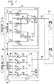
- FIG. 1 shows a block diagram of a coherent optical communication system 100 according to an embodiment.
- System 100 has an optical transmitter 110 and a coherent optical receiver 190 coupled to one another via an optical communication link 140.
- Transmitter 110 and receiver 190 may also be connected to one another by way of a control link 180, which can be used, e.g., by the receiver and/or transmitter to send service messages and/or control signals.
- control link 180 can be implemented using the control plane of system 100 and/or over an Internet connection.
- Control link 180 can be used, e.g., for ANN training purposes and/or to enable transmitter 110 and receiver 190 to operate in a collaborative manner.
- system 100 can operate in a payload mode and a training mode.
- system 100 uses pilot data sequences "known" to both transmitter 110 and receiver 190 to perform, inter alia, geometric constellation shaping, e.g., as described below in reference to FIGs. 10-13 .
- constellation shaping may include but is not limited to the steps of: (i) selecting and/or changing the size of the constellation; (ii) changing the position of one or more constellation points on the IQ plane; (iii) changing a respective binary label (e.g., bit-word) of one or more constellation points; and (iv) using a set of predetermined criteria to drive the changes made at steps (ii) and (iii).
- An example outcome upon the completion of a training-mode run can be a fixed constellation, wherein each constellation point has a respective fixed position on the IQ plane and a respective fixed binary label (e.g., a bit-word of selected length) assigned thereto (see, e.g., FIG. 12 ).
- the fixed binary label is the bit-word encoded by the constellation point. This fixed constellation can then be used for data transmission during a payload mode.
- transmitter 110 receives a digital electrical input stream 102 of payload data and applies it to a digital signal processor (DSP) 112.
- DSP 112 processes input data stream 102 to generate digital signals 114 1 -114 4 .
- DSP 112 may perform, inter alia, one or more of the following: (i) de-multiplex input stream 102 into two sub-streams, each intended for optical transmission using a respective one of the orthogonal (e.g., X and Y) polarizations of an optical output signal 130; (ii) encode each of the sub-streams using a suitable forward-error-correction (FEC) code, e.g., to enable error correction at receiver 190; and (iii) convert each of the two resulting sub-streams into a corresponding sequence of constellation symbols of the fixed constellation determined during the training mode.
- FEC forward-error-correction
- signals 114 1 and 114 2 carry digital values that represent the inphase (I) component and quadrature (Q) component, respectively, of a corresponding constellation symbol intended for transmission using a first (e.g., X) polarization of light.
- signals 114 3 and 114 4 similarly carry digital values that represent the I and Q components, respectively, of the corresponding constellation symbol intended for transmission using a second (e.g., Y) polarization of light.
- An E/O converter 116 (also sometimes referred to as a front end or front-end circuit) of transmitter 110 operates to transform digital signals 114 1 -114 4 into a corresponding modulated optical output signal 130. More specifically, drive circuits 118 1 and 118 2 transform digital signals 114 1 and 114 2 , as known in the art, into electrical analog drive signals I X and Q X , respectively, for the corresponding signaling interval. Drive signals I X and Q X are then used, in a conventional manner, to drive an I-Q modulator 124 X . In response to drive signals I X and Q X , I-Q modulator 124 X operates to modulate an X-polarized beam 122 X of light supplied by a laser source 120 as indicated in FIG. 1 , thereby generating a modulated optical signal 126 X .
- Drive circuits 118 3 and 118 4 similarly transform digital signals 1 14 3 and 114 4 into electrical analog drive signals I Y and Q Y , respectively, for the corresponding signaling interval.
- an I-Q modulator 124 Y operates to modulate a Y-polarized beam 122 Y of light supplied by laser source 120 as indicated in FIG. 1 , thereby generating a modulated optical signal 126 Y .
- a polarization beam combiner 128 operates to combine modulated optical signals 126 X and 126 Y , thereby generating optical output signal 130.
- Optical output signal 130 is then applied to optical communication link 140.
- a drive circuit 118 may include a digital-to-analog converter (DAC, not explicitly shown in FIG. 1 ).
- DAC digital-to-analog converter
- Optical communication link 140 is illustratively shown as being an amplified optical link having a plurality of optical amplifiers 144 configured to amplify the optical signals that are being transported through the optical fiber(s) of the link, e.g., to counteract signal attenuation in the fiber spans thereof. Note that optical communication link 140 that has only one or even no optical amplifiers 144 can similarly be used in an alternative embodiment. After propagating through optical communication link 140, optical signal 130 becomes optical signal 130', which is applied to receiver 190.
- Optical signal 130' may differ from optical signal 130 because optical communication link 140 typically adds noise and imposes various signal distortions, e.g., due to to optical amplifier(s) and/or due to chromatic dispersion, polarization rotation, polarization-mode dispersion, and/or nonlinear optical effects, e.g., in optical fiber(s).
- Receiver 190 has a front-end circuit 172 comprising an optical-to-electrical (O/E) converter 160, analog-to-digital converters (ADCs) 166 1 -166 4 , and an optical local-oscillator (OLO) source 156.
- O/E converter 160 has (i) two input ports labeled S and R and (ii) four output ports labeled 1 through 4.
- Input port S receives optical signal 130' from optical communication link 140.
- Input port R receives an OLO signal 158 generated by OLO source 156.
- OLO signal 158 has an optical-carrier frequency (wavelength) that is sufficiently close to that of signal 130' to enable coherent (e.g., intradyne) detection of the latter signal.
- OLO signal 158 can be generated, e.g., using a relatively stable tunable laser whose output wavelength (frequency) is approximately the same as the carrier wavelength (frequency) of optical signal 130'.
- O/E converter 160 operates to mix input signal 130' and OLO signal 158 to generate eight different mixed (e.g., by interference) optical signals (not explicitly shown in FIG. 1 ), e.g., eight such mixed signals for differential I/Q detection for two polarizations.
- O/E converter 160 then uses one or more photodetectors (e.g., one or more photodiodes, not explicitly shown in FIG. 1 ) to convert the set of mixed optical signals into four electrical signals 162 1 -162 4 that are indicative of complex values corresponding to the two orthogonal-polarization components of signal 130'.
- electrical signals 162 1 and 162 2 may be an approximate analog I signal and an approximate analog Q signal, respectively, corresponding to a first (e.g., horizontal, h) polarization component of signal 130'.
- Electrical signals 162 3 and 162 4 may similarly be an approximate analog I signal and an approximate analog Q signal, respectively, corresponding to a second (e.g., vertical, v) polarization component of signal 130'.
- the orientation of the h and v polarization axes at receiver 190 may or may not coincide with the orientation of the X and Y polarization axes at transmitter 110.
- the signal-mixing functionality of O/E converter 160 can be implemented using one or more optical hybrids.
- Each of electrical signals 162 1 -162 4 generated by O/E converter 160 is converted into digital form in a corresponding one of ADCs 166 1 -166 4 .
- each of electrical signals 162 1 -162 4 may be amplified in a corresponding electrical amplifier (e.g., a transimpedance amplifier, TIA; not explicitly shown in FIG. 1 ) prior to the resulting signal being converted into digital form.
- Digital signals 168 1 -168 4 produced by ADCs 166 1 -166 4 are then processed by a DSP 170 to recover the data of the original input data stream 102 applied to transmitter 110.
- DSP 170 may perform, inter alia, one or more of the following: (i) electronic polarization de-multiplexing; (ii) signal equalization and/or dispersion compensation; (iii) mapping signal samples onto the fixed constellation determined during the training mode; and (iv) error correction based on the FEC encoding applied at DSP 112.
- each of DSP 112 and DSP 170 includes a respective ANN.
- Example embodiments of DSP 112 and DSP 170 and the pertinent signal-processing method(s) that can be implemented therein are described in more detail below in reference to FIGs. 2-13 .
- ANN refers to a distributed and typically nonlinear trainable circuit or machine constructed using a plurality of processing elements (PEs). Also, an ANN may be dynamically adaptive. Each PE has connections with one or more other PEs. The plurality of connections between the PEs defines the ANN's topology. In some topologies, the PEs may be aggregated into layers. Different layers may have different types of PEs configured to perform different respective kinds of transformations on their inputs. Signals may travel from the first PE layer (typically referred to as the input layer) to the last PE layer (typically referred to as the output layer). In some topologies, the ANN may have one or more intermediate PE layers (typically referred to as the hidden layers) located between the input and output PE layers.
- An example PE may scale, sum, and bias the incoming signals and use an activation function to produce an output signal that is a static nonlinear function of the biased sum.
- the resulting PE output may become either one of the ANN's outputs or be sent to one or more other PEs through the corresponding connection(s).
- the respective weights and/or biases applied by individual PEs can be changed during the training mode and are typically fixed (constant) during the payload mode.
- ANN Artificial Neural Networks with Comparison to Other Networks
- an ANN can be implemented using one or more of the following: (i) a software program executed by a general-purpose or specialized electronic processor; (ii) a field-programmable gate-array (FPGA) device; and (iii) an application-specific integrated circuit (ASIC).
- Some ANNs can be implemented using an optical processor, e.g., as described in U.S. Patent No. 7,512,573 , which is incorporated herein by reference in its entirety.
- a PE can be implemented using one or more of the following electrical circuits: (i) a multiplier circuit; (ii) an adder; (iii) a comparator; and (iv) a nonvolatile-memory cell.
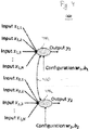
- FIG. 2 schematically illustrates a block diagram of a PE 200 that can be used in DSP 112 and/or DSP 170 according to an embodiment.
- PE 200 is a multiple-input/single-output (MISO) device having N inputs (labeled x 1 , x 2 , ..., x N ) and a single output (labeled y ), where N is a positive integer greater than one.
- MISO multiple-input/single-output
- the configuration of PE 200 is determined by the weight vector w , the bias b, and the scalar function f ( ⁇ ).
- the weight vector w ( 1 , w 2 , ..., w N ) T has N scalar components.
- the functions defined by Eqs. (2a)-(2e) are also sometimes referred to as the rectified linear unit (ReLU) function, leaky rectified linear unit (LReLU) function, sigmoid function, hyperbolic tangent function, and Gudermannian function, respectively.
- multiple copies of the output y may be generated and applied to the respective input ports of the corresponding different PEs connected to PE 200.
- FIG. 3 schematically illustrates a block diagram of a PE 300 that can be used in DSP 112 according to an embodiment.
- PE 300 may sometimes be referred to as the "normalization node.”
- the scaling variable ⁇ may not be used as a separate PE-configuration parameter, but rather be incorporated into each of the weight vector w and the bias b by redefining those quantities as ⁇ w and ⁇ b, respectively.
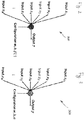
- FIG. 4 schematically illustrates a block diagram of a group 400 of PEs 410 that can be used in DSP 170 according to an embodiment.
- a group 400 may have G PEs 410, where G is a positive integer greater than one.
- G is a positive integer greater than one.
- the corresponding two PEs 410 are labeled in FIG. 4 as 410 1 and 410 2 , respectively.
- An individual PE 410 may sometimes be referred to as the "softmax node.”
- input bit-stream 502 carries a pilot data sequence.
- input bit-stream W 502 carries payload data and can be generated, e.g., by demultiplexing input stream 102 ( FIG. 1 ).
- Circuit 500 comprises an FEC encoder 510 that uses a suitable FEC code, as known in the pertinent art, to add redundancy to input bit-stream 502, thereby converting the latter into an FEC-encoded bit-stream 512.
- a serial-to-parallel (S/P) converter 520 then converts bit-stream 512 into a plurality of bit-streams 522 1 -522 m , where m is a positive integer grater than one.
- S/P converter 520 can be a demultiplexer. In some other embodiments, S/P converter 520 can be configured to implement a more-complex linear transformation of bit-stream 502 into bit-streams 522 1 -522 m . For example, such more-complex transformation may include, e.g., data interleaving, suitable linear matrix operations, etc.
- Circuit 500 further comprises an ANN 530 and a look-up table (LUT) 560, each of which is connected to receive a respective copy of bit-streams 522 1 -522 m .
- the state of a switch 540 determines whether the outputs of ANN 530 or the outputs of LUT 560 are used to generate digital signals 114 a and 114 b .
- an electronic controller 560 is configured to use a control signal 554 to cause switch 540 to: (i) use the outputs of ANN 530 during the training mode and (ii) use the outputs of LUT 560 during the payload mode.
- LUT 560 may not be used and, as such, can be disabled, disconnected, or removed from circuit 500.
- the outputs of ANN 530 are used to generate digital signals 114 a and 114 b in both training and payload modes.
- controller 550 can use a control signal 552 to change the PE-configuration parameters of ANN 530 during the training mode, e.g., as described in reference to FIG. 10 .
- the PE-configuration parameters of ANN 530 remain constant during the payload mode.
- ANN 530 uses the respective input bit-word provided by the bits of bit-streams 522 1 -522 m to generate an output symbol, the I-component of which is carried by a digital output signal 532 1 , and the Q-component of which is carried by a digital output signal 532 2 .
- the conversion of the input bit-word into the I and Q values performed by the ANN is deterministic. That is: the same input bit-word received via bit-streams 522 1 -522 m results in the same (I,Q) pair for digital output signals 532 1 and 532 2 .
- the latter property of ANN 530 can beneficially be used to reduce the computational load of DSP 112 using LUT 560 instead of ANN 530.
- controller 550 can use control signals 534 and 556 to load LUT 560 by saving therein a respective (I,Q) pair for each different input bit-word. Then, during the payload mode, the saved (I,Q) pairs can be read out from LUT 560 and applied to LUT outputs 562 1 and 562 2 to reproduce the response of ANN 530 to the same input bit-words.
- LUT 560 instead of ANN 530 can reduce the computational load in circuit 500, e.g., because a LUT is typically a simpler circuit than an ANN.
- FIG. 6 shows a block diagram of ANN 530 according to an embodiment. Digital signals 522 1 -522 m and 532 1 -532 2 are also shown in FIG. 6 to better illustrate the relationship between the circuits of FIGs. 5 and 6 .
- ANN 530 comprises one-hot vector encoders 610 1 -610 m , each configured to receive a respective one of digital signals 522 1 -522 m .
- ANN 530 further comprises an input layer 616, a bit-level section 640, a symbol-level section 650, and an output layer 660.
- Input layer 616 comprises a plurality of PEs 620, each pair of which is connected to a respective one of encoders 610 1 -610 m .
- the output of each PE 620 is copied an appropriate number of times, and the resulting copies are applied to PEs 200 of a corresponding portion 630 of section 640.
- each PE 620 can be implemented using a suitable embodiment of PE 200 ( FIG. 2 ) or PE 300 ( FIG. 3 ).
- each PE 620 may be configured to simply generate multiple copies of its input and apply each copy to a respective one of its outputs.
- Each portion 630 may have two or more layers of fully connected PEs 200.
- the term "fully connected” should be interpreted to mean that the output of a PE 200 of one PE layer of portion 630 is received by each PE 200 of the next PE layer of that portion 630.
- FIG. 6 shows only two PE layers in each portion 630. However, a person of ordinary skill in the art will readily understand how to connect additional PE layers therein.
- Different portions 630 of section 640 are not directly connected to one another.
- PEs 200 of portion 630 1 do not apply any of their outputs to any PEs 200 of portion 630 2 or 630 m .
- PEs 200 of portion 630 2 do not apply any of their outputs to any PEs 200 of portion 630 1 or 630 m , etc.
- each of portions 630 1 -630 m responds only to the corresponding one of digital signals 522 1 -522 m , and does not respond to any other ones of those digital signals.
- Section 650 may comprise two or more layers of fully connected PEs 200.
- a PE 200 of the first PE layer of section 650 is connected to receive outputs from each PE 200 of the last PE layers of portions 630 1 -630 m .
- FIG. 6 shows only two PE layers in section 650. However, a person of ordinary skill in the art will readily understand how to connect additional PE layers therein.
- section 650 may have a single layer of PEs 200.
- Output layer 660 comprises two PEs 300, each connected to receive outputs from each PE 200 of the last PE layer of section 650.
- the output of one PE 300 of output layer 660 is digital signal 532 1 (also see FIG. 5 ).
- the output of the other PE 300 of output layer 660 is digital signal 532 2 (also see FIG. 5 ).
- ANN 530 shown in FIG. 6 is designed to process two-dimensional constellation symbols, e.g., represented by the I and Q components (corresponding to the two dimensions on the complex plane).
- possible embodiments of the ANNs that can be used in system 100 are not so limited. From the provided description, a person of ordinary skill in the art will be able to make and use other embodiments, in which the corresponding ANNs are configured to process constellation symbols whose dimensionality differs from two.
- the term "constellation symbol” should be construed to encompass both constellation symbols of a one-dimensional constellation and of a multi-dimensional constellation.
- An example one-dimensional constellation enables the transmission of a single constellation symbol in a single signaling interval (time slot) over a single dimension of the carrier.
- a multi-dimensional constellation enables the transmission of a single constellation symbol using multiple signaling intervals and/or multiple dimensions of the carrier and/or link.
- a d-dimensional constellation can be constructed using d different one-dimensional constellations or d copies of the same one-dimensional constellation. Examples of possible dimensions that can be used for these purposes include but are not limited to time, quadrature, polarization, spatial mode, and carrier frequency.
- FIGs. 5-6 can be modified to be able to process four-dimensional constellation symbols, which can then be transmitted using two orthogonal (e.g., X and Y) polarizations of the carrier.
- These modifications may, e.g., include the following.
- S/P converter 520 can be modified to convert bit-stream 512 into 2m bit-streams 522 1 -522 2m .
- ANN 530 can be modified to generate four digital output signals, wherein digital output signals 532 1 -532 2 provide values for the I- and Q-components, respectively, of the X-polarization, and the two additional digital output signals provide values for the I- and Q-components, respectively, of the Y-polarization.
- LUT 560 can be modified to have 2m inputs and four outputs.
- Switch 540 can be modified to generate digital signals 114 1 -114 4 (also see FIG. 1 ) by selecting either the four outputs of the modified ANN 530 or the four outputs of the modified LUT 560.
- FIG. 7 shows a block diagram of a digital circuit 700 that can be used in DSP 170 of receiver 190 ( FIG. 1 ) according to an embodiment.
- circuit 700 converts digital signals 168 1 -168 4 ( FIG. 1 ) into output bit-stream 502 (also see FIG. 5 ).
- Circuit 700 comprises a receiver-processing circuit 710 configured to convert digital signals 168 1 -168 4 into digital signals 712 1 -712 4 .
- the signal processing implemented in circuit 710 may include some of the signal-processing operations performed in the DSP chain of conventional coherent optical receivers prior to constellation demapping. Such signal-processing operations may include, e.g., one or more of the following: (i) reduction of signal distortions caused by front-end circuit 172 ( FIG. 1 ); (ii) electronic polarization rotation and/or demultiplexing; (iii) clock recovery; (iv) OLO phase and/or frequency-offset correction, etc.
- Circuit 700 further comprises an ANN 720 and a demapping circuit 770, each of which is connected to receive a respective copy of digital signals 712 1 -712 4 .
- the state of a switch 730 determines whether the outputs of ANN 720 or the outputs of demapping circuit 770 are applied to a parallel-to-serial (P/S) converter 740.
- P/S parallel-to-serial
- an electronic controller 760 is configured to use a control signal 764 to cause switch 730 to pass through: (i) the outputs of ANN 720 during the training mode, and (ii) the outputs of demapping circuit 770 during the payload mode.
- demapping circuit 770 may not be used and, as such, can be disabled, disconnected, or removed from circuit 700.
- the outputs of ANN 720 are applied to P/S converter 740 in both training and payload modes.
- controller 760 can use a control signal 762 to change the PE-configuration parameters of ANN 720 during the training mode, e.g., as described in reference to FIG. 10 .
- the PE-configuration parameters of ANN 720 remain constant during the payload mode.
- ANN 720 uses two respective (I,Q) pairs provided by the input digital signals ( 712 1 , 712 2 ) and ( 712 3 , 712 4 ), respectively, to generate two corresponding bit-words, each having m bits.
- the m bits of the first of the two bit-words is carried by digital output signals 722 1 -722 m .
- the m bits of the second of the two bit-words is carried by digital output signals 722 m+1 -722 2m .
- the conversion of each of the input (I,Q) pairs performed by the ANN can be alternatively represented by a mapping operation configured to use a respective plurality of decision maps, each corresponding to a respective bit of the output bit-word.
- Each of the decision maps divides the I-Q plane into two portions, the first portion representing the binary "one,” and the second portion representing the binary "zero.”
- the input (I,Q) pair provided by the input digital signals ( 712 1 , 712 2 ) or ( 712 3 , 712 4 ) can then be used as the coordinates of the corresponding sample point on each of the decision maps to convert that (I,Q) pair into the output bit-word as follows.
- the map-based representation of the conversion performed by ANN 720 can beneficially be used to reduce the computational load of DSP 170 using demapping circuit 770 instead of ANN 720.
- controller 760 can use control signals 724 and 766 to: (i) generate the above-described decision maps using the PE configuration parameters of ANN 720; and (ii) load the generated decision maps into demapping circuit 770.
- the loaded decision maps can be used by demapping circuit 770 to perform the above-described conversion of the input (I,Q) pairs provided thereto by the input digital signals ( 712 1 , 712 2 ) and ( 712 3 , 712 4 ) to reproduce the response of ANN 720 to the same input (I,Q) pairs.
- the resulting bit-words are then used to generate digital output signals 772 1 -772 2m .
- the m bits of the first of the two bit-words is carried by digital output signals 772 1 -772 m
- the m bits of the second of the two bit-words is carried by digital output signals 772 m+1 -772 2m .
- the use of demapping circuit 770 instead of ANN 720 may reduce the computational load in circuit 700, e.g., because at least some mapping circuits may be less complicated than ANN 720.
- a parallel-to-serial (P/S) converter 740 operates to serialize bit-streams 732 1 -732 2m outputted by switch 730, thereby generating a bit-streams 742.
- the serialization operation performed by P/S converter 740 is configured to be the inverse of the de-serialization operations performed by the corresponding S/P converter 520 ( FIG. 5 ) located at transmitter 110 ( FIG. 1 ).
- bit-stream 742 is the same as bit-stream 512.
- An FEC decoder 750 operates to apply the operative FEC code to correct errors and remove redundancy from bit-stream 742, as known in the pertinent art, thereby recovering bit-stream 502 (also see FIG. 5 ).
- FIG. 8 shows a block diagram of an ANN 800 that can be used to implement ANN 720 according to an embodiment.
- ANN 800 is shown to process digital signals 712 1 and 712 2 and to generate digital signals 722 1 -722 2 .
- ANN 800 can be used to process signals in a manner compatible with the processing implemented in ANN 530 (see FIGs. 5-6 ).
- ANN 800 can be modified in a straightforward manner, e.g., as described further below, to process digital signals 712 1 -712 4 and to generate digital signals 722 1 -722 2m for processing signals corresponding to two polarizations.
- ANN 800 comprises a symbol-level section 810, a bit-level section 820, and an output layer 840.
- Section 810 may comprise two or more layers of fully connected PEs 200.
- a PE 200 of the first PE layer of section 810 is connected to respective copies of input digital signals 712 1 and 712 2 .
- a PE 200 of the last PE layer of section 810 is connected to apply copies of its output to each PE 200 of the first PE layer of section 820.
- FIG. 8 shows three PE layers in section 810. However, a person of ordinary skill in the art will readily understand how to connect additional PE layers therein or to remove one PE layer.
- section 810 may comprise a single layer of PEs 200.
- Section 820 comprises portions 830 1 -830 m . Different portions 830 of section 820 are not directly connected to one another. For example, PEs 200 of portion 830 1 do not apply any of their outputs to any PEs 200 of portion 830 2 or 830 m . PEs 200 of portion 830 2 do not apply any of their outputs to any PEs 200 of portion 830 1 or 830 m , etc.
- arg-max circuit 850 j operates to: (i) compare the outputs of the two PEs 410 of group 400 j and (ii) generate a binary value for output bit-stream 722 j based on the comparison.
- arg-max circuit 850 j generates a binary "zero" for output bit-stream 722 j . Otherwise, arg-max circuit 850 j generates a binary "one" for output bit-stream 722 j .
- ANN 800 can be modified, e.g., as follows.
- Section 810 can be modified to receive four digital signals 712 1 -712 4 .
- Section 820 can be modified to have 2m portions 830.
- Output layer 840 can be modified to have 2m groups 400, and the number of arg-max circuits 850 can accordingly be increased to 2m.
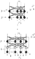
- FIGs. 9A-9B illustrate a circuit modification that can be used to implement any or all of ANNs 530, 720, and 800 according to an embodiment. More specifically, FIG. 9A shows a block diagram of an ANN portion 910 that can be used in some of the above-described embodiments of ANNs 530, 720, and 800. FIG. 9B shows a block diagram of an ANN portion 940 that can be used to replace ANN portion 910 in some embodiments of ANNs 530, 720, and 800.
- ANN portion 910 has two layers of PEs 200, which are labeled 920 1 and 920 2 , respectively.
- ANN portion 910 converts an input vector X 1 into an output vector X 3 in accordance with Eqs. (6)-(7):
- X 3, i is the i-th component of the output vector X 3 ;
- f a is the ReLU function (also see Eq.
- W 2 , i is the weight vector used in the i-th PE 200 in PE layer 920 2 ;
- X 2 is the output vector generated by PE layer 920 1 ;
- b 2, i is the bias used in the i-th PE 200 in PE layer 920 2 ;
- X 2,i is the i-th component of the output vector X 2 ;
- W 1, i is the weight vector used in the i-th PE 200 in PE layer 920 1 ;
- b 1, i is the bias used in the i-th PE 200 in PE layer 920 1 ;
- ANN portion 940 uses a PE layer 950 instead of PE layer 920 2 .
- the signal conversion performed by ANN portion 940 is described by Eqs. (6) and (8).
- each PE 900 is connected to receive a corresponding scalar component of the input vector X 1 in addition to the full vector X 2 .
- the use of one or more ANN portions 940 in system 100 may be beneficial because such use may help to improve the system's training process and/or increase the speed of convergence of the optimization algorithm(s) used therefor.
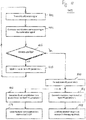
- FIG. 10 shows a flowchart of a communication method 1000 that can be used in system 100 during a training mode according to an embodiment.
- the description of some steps of method 1000 may also refer to the specific examples shown in FIGs. 11-13 .
- system 100 is operated to transmit from transmitter 110 to receiver 190 a calibration signal 130 (also see FIG. 1 ).
- calibration signal 130 may carry pilot data sequences specifically designed, e.g., as known in the pertinent art, for ANN training purposes, wherein the transmitted forms of the pilot data sequences are known by both transmitter 110 and the receiver 190.
- pilot data sequences specifically designed, e.g., as known in the pertinent art, for ANN training purposes, wherein the transmitted forms of the pilot data sequences are known by both transmitter 110 and the receiver 190.
- control link 180 FIG. 1
- the system controller (e.g., including controllers 550 and 760 and/or other pertinent entities corresponding to the control plane of system 100 ) computes a cost function L ( ⁇ ) based on at least some of the above-indicated signals (see, e.g., FIGs. 5-8 ) generated by transmitter 110 and receiver 190 during step 1002.
- An example cost function L ( ⁇ ) that is suitable for this purpose is given by Eq. (9) L B 1 ... B m Z 1 ...
- the cost function L ( ⁇ ) and/or the PE-parameter-update algorithm(s) used at step 1008 may rely on an approximate mathematical model of link 140 ( FIG. 1 ).
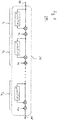
- FIG. 11 shows a schematic representation of an example mathematical model 1100 of optical link 140 that can be used in method 1000 according to an embodiment.
- Model 1100 corresponds to an optical link characterized by zero dispersion and the nonlinearity coefficient ⁇ .
- the value of the nonlinearity coefficient ⁇ can be 1.27 W/km.
- Model 1100 represents optical link 140 as K serially connected stages S 1 , S 2 , ..., S K . Each of these stages represents a section of optical fiber of length L / K , where L is the total length of fiber in link 140.
- other possible optical links 140 may have chromatic dispersion and/or nonlinear optical effects and, as such, may be modeled differently.
- each stage S k on the optical signal applied thereto is to: (i) impose a phase rotation, the magnitude of which is proportional to the intensity (squared amplitude of the electrical field) of the optical signal; and (ii) add Gaussian noise.
- the Gaussian noise imposed by stage S k is denoted therein as n k .
- An example value of K can be between 10 and 100.
- link 140 can also be used and will be able to select or construct a suitable mathematical model based on the specific technical characteristics of link 140.
- the system controller uses a predefined set of one or more criteria to evaluate the cost function L ( ⁇ ) computed at step 1004. If the criteria are not satisfied, then the processing of method 1000 is directed to step 1008. If the criteria are satisfied, then the processing of method 1000 is directed to step 1010.
- step 1006 may include one or more of the following: (i) comparing the value of the cost function L ( ⁇ ) with one or more predetermined threshold values; (ii) comparing a change in the value of the cost function L ( ⁇ ) corresponding to two different executions of the processing loop 1002-1008 with one or more other predetermined threshold values; etc.
- the system controller may use a suitable algorithm to change one or more PE-configuration parameters (e.g., see Eqs. (1), (3), (4), and (6)-(8)).
- a suitable algorithm may be directed at minimizing the cost function L ( ⁇ ) and may rely, inter alia, on a mathematical model of optical link 140 (e.g., see FIG. 11 ).
- the processing of method 1000 is directed back to step 1002.
- the system controller causes the present values of the PE-configuration parameters to be fixed, e.g., by disabling further configuration updates. These parameters values may also be saved in a non-volatile memory for future use, e.g., during the payload mode.
- Steps 1012 and 1014 may be optional and may be executed in embodiments in which LUT 560 is used during the payload mode.
- controller 550 uses the PE-configuration parameters of step 1010 to generate a fixed constellation.
- controller 550 may apply a set of different bit-words to ANN 530 using digital signals 522 1 -522 m and then use digital signals 532 1 -532 2 to determine the I and Q values corresponding to each such bit-word (also see FIG. 5 ).
- the (I,Q) pairs determined in this manner provide the coordinates of the different constellation points of the constellation defined by the fixed PE-configuration parameters. For each of such constellation points, the corresponding input bit-word applied to ANN 530 via digital signals 522 1 -522 m provides the respective binary label.
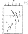
- the relative arrangement of constellation points in constellation 1200 may be irregular in the sense that the constellation points are not located on an regular square or rectangular grid, as is the case, e.g., for a conventional 16-QAM constellation.
- Two groups of constellation points can be noticed.
- a first group (labeled 1210 ) has ten constellation points, each having a relatively small amplitude.
- a second group (labeled 1220 ) has six constellation points, each having a relatively large amplitude, with the points being in an approximately linear formation.
- the binary labels in each group are quasi-Gray in nature.
- constellation 1200 can be qualitatively understood, for example, as follows. For relatively small signal amplitudes, signal distortions in channel 1100 are dominated by the Gaussian noise. In this case, an optimal performance can be achieved by appropriately spreading the constellation around the origin, e.g., as in group 1210. For relatively large signal amplitudes, signal distortions in channel 1100 are dominated by the nonlinear phase noise. In this case, an optimal performance can be achieved by appropriately limiting the possible phase values, e.g., as in group 1220.
- an optical channel that is different from channel 1100 may cause system 100 to converge, during training, on a constellation having a different set of geometric characteristics than constellation 1200.
- step 1014 of method 1000 the results of step 1012 may be loaded into LUT 560.
- Steps 1016 and 1018 may be optional and may be executed in embodiments in which demapping circuit 770 ( FIG. 7 ) is used during the payload mode.
- controller 760 uses the PE-configuration parameters of step 1010 to generate a set of decision maps corresponding to the constellation of step 1012. For example, controller 760 may generate a set of (I,Q) pairs corresponding to the nodes of a relatively tight square or rectangular grid covering the I-Q plane. In this case, the distance between the adjacent grid lines typically determines the resolution of the resulting decision maps.
- controller 760 may apply the different (I,Q) pairs corresponding to the nodes of the grid to ANN 800 1 using digital signals 712 1 -712 2 and then use digital signals 722 1 -722 m to determine the bit-words corresponding to each such (I,Q) pair (also see FIG. 8 ). In this manner, the bit value for each of the m bit positions can be determined for each (I,Q) pair. Appropriate extrapolation and/or interpolation techniques may optionally be used to obtain the bit values for the points that are located between the nodes of the used grid. The resulting body of data can then be converted into decision maps in a relatively straightforward manner.
- the decision maps generated at step 1016 may be loaded into demapping circuit 770.
- an apparatus comprising: an optical data transmitter (e.g., 110, FIG. 1 ) that includes: an optical modulator (e.g., 124, FIG. 1 ), one or more electrical drivers (e.g., 118, FIG. 1 ) connected to operate the optical modulator to modulate an optical carrier to carry a stream of digital symbols (e.g., I and Q values, FIG. 5 ), and a digital signal processor (e.g., 112, FIG.
- an optical data transmitter e.g., 110, FIG. 1
- an optical modulator e.g., 124, FIG. 1
- one or more electrical drivers e.g., 118, FIG. 1
- a digital signal processor e.g., 112, FIG.
- the digital signal processor configured to use an artificial neural network (e.g., 530, FIG. 5 ) to determine values of the digital symbols corresponding to values of input bit-words applied to a plurality of inputs (e.g., 522 1 -522 m , FIG. 5 ) of the artificial neural network, each of the inputs being configured to carry a respective bit of the input bit-words to a different respective portion (e.g., one of 630 1 -630 m , FIG. 6 ) of the artificial neural network, each of the portions being configured to respond to a respective one of the inputs.
- an artificial neural network e.g., 530, FIG. 5
- the digital signal processor configured to use an artificial neural network (e.g., 530, FIG. 5 ) to determine values of the digital symbols corresponding to values of input bit-words applied to a plurality of inputs (e.g., 522 1 -522 m , FIG. 5 ) of the artificial neural network, each of the inputs
- different ones of the respective portions are separate.
- the artificial neural network further comprises a plurality of processing elements (e.g., the first layer of 650, FIG. 6 ), wherein each of said processing elements is connected to receive digital inputs from each of the respective portions (e.g., as indicated in FIG. 6 ).
- the apparatus further comprises an electronic controller (e.g., 550, FIG. 5 ) configured to change configuration parameters of the artificial neural network based on a training mode in which the optical data transmitter transmits pilot data sequences through an optical fiber (e.g., 140, FIG. 1 ).
- an electronic controller e.g., 550, FIG. 5
- the optical data transmitter transmits pilot data sequences through an optical fiber (e.g., 140, FIG. 1 ).
- the electronic controller is further configured to fix the configuration parameters of the artificial neural network for a payload mode in which the transmitter transmits a modulated optical carrier carrying the input data to the optical fiber.
- the apparatus further comprises a look-up table (e.g., 560, FIG. 5 ) having stored therein values of the digital symbols (e.g., I and Q values, FIG. 5 ) for different values of the input bit-words; and wherein the electronic controller is further configured to load (e.g., at 1014, FIG. 10 ) the values of the digital symbols for the different values of the input bit-words into the look-up table based on the training mode.
- a look-up table e.g., 560, FIG. 5
- the electronic controller is further configured to load (e.g., at 1014, FIG. 10 ) the values of the digital symbols for the different values of the input bit-words into the look-up table based on the training mode.
- the apparatus further comprises a look-up table (e.g., 560, FIG. 5 ) connected to the plurality of inputs and configured to output the values of the digital symbols in response to the values of the input bit-words.
- a look-up table e.g., 560, FIG. 5
- the apparatus further comprises a switch (e.g., 540, FIG. 5 ) configured to select the values of the digital symbols generated by the artificial neural network or the values of the digital symbols generated by the look-up table.
- a switch e.g., 540, FIG. 5
- the apparatus further comprises a forward-error-correction encoder (e.g., 510, FIG. 5 ) configured to generate a stream of input bit-words for the plurality of electrical inputs by applying a forward-error-correction code to an input data stream (e.g., 502, FIG. 5 ).
- a forward-error-correction encoder e.g., 510, FIG. 5
- an input data stream e.g., 502, FIG. 5
- the apparatus further comprises an optical data receiver (e.g., 190, FIG. 1 ) that includes an optical-to-electrical converter (e.g., 160, FIG. 1 ), a plurality of analog-to-digital converters (e.g., 166, FIG. 1 ), and a second digital signal processor (e.g., 170, FIG. 1 ), the analog-to-digital converters being configured to output a stream of digitalizations of measurements of the modulated optical carrier, the measurements being performed by the optical-to-electrical converter; and wherein the second digital signal processor is electrically connected to process the stream of digitalizations using a second artificial neural network (e.g., 800, FIG. 8 ).
- a second artificial neural network e.g., 800, FIG. 8
- the digital signal processor is configured to determine the values of the digital symbols using a d-dimensional constellation, where d is an integer greater than two.
- the digital signal processor is electrically connected to control the one or more associated electrical drivers and comprises an artificial neural network (e.g., 530, FIG. 5 ) configured to: receive an input bit-word on a plurality of electrical inputs (e.g., 522 1 -522 m , FIG. 5 ), each of the electrical inputs being configured to carry a different respective bit of the input bit-word to a different respective portion (e.g., one of 630 1 -630 m , FIG. 6 ) of the artificial neural network, each of the different respective portions being configured to respond to a respective single one of the electrical inputs; and generate an output digital symbol (e.g., I and Q values, FIG. 5 ) for the digital-symbol stream in response to the input bit-word.
- an artificial neural network e.g., 530, FIG. 5
- receive an input bit-word on a plurality of electrical inputs e.g., 522 1 -522 m , FIG. 5
- the artificial neural network comprises a plurality of interconnected processing elements (e.g., 200, 300, 620, FIG. 6 ); and wherein any two of the different respective portions have no processing elements in common.
- the electronic controller is further configured to load constellation data (e.g., at 1014, FIG. 10 ) into the look-up table; and wherein the look-up table is configured to use the constellation data to replicate the output digital symbol generated by the artificial neural network in response to the input bit-word.
- constellation data e.g., at 1014, FIG. 10
- the apparatus further comprises an optical data receiver (e.g., 190, FIG. 1 ) that includes an optical-to-electrical converter (e.g., 160, FIG. 1 ), a plurality of analog-to-digital converters (e.g., 166, FIG. 1 ), and a second digital signal processor (e.g., 170, FIG. 1 ), the analog-to-digital converters being configured to output a stream of digitalizations of measurements of the modulated optical carrier, the measurements being performed by the optical-to-electrical converter; and wherein the second digital signal processor is electrically connected to process the stream of digitalizations and comprises a second artificial neural network (e.g., 800, FIG.
- a second artificial neural network e.g., 800, FIG.
- each of the electrical outputs being configured to carry a different respective bit of the output bit-word generated by a different respective portion (e.g., one of 400 1 -400 m , FIG. 6 ) of the second artificial neural network, each of the different respective portions of the second artificial neural network being connected to control a respective single one of the electrical outputs.
- an apparatus comprising: a coherent optical data receiver (e.g., 190, FIG. 1 ) that includes an optical-to-electrical converter (e.g., 160, FIG. 1 ) for a modulated optical carrier, a plurality of analog-to-digital converters (e.g., 166, FIG. 1 ), and a digital signal processor (e.g., 170, FIG.
- a coherent optical data receiver e.g., 190, FIG. 1
- an optical-to-electrical converter e.g., 160, FIG. 1
- analog-to-digital converters e.g., 166, FIG. 1
- digital signal processor e.g., 170, FIG.
- the analog-to-digital converters being configured to output a stream of digitalizations of measurements of the modulated optical carrier performed by the optical-to-electrical converter; and wherein the digital signal processor is electrically connected to process the stream of digitalizations using an artificial neural network (e.g., 800, FIG. 8 ) configured to generate a stream of output bit-words on a plurality of outputs (e.g., 722 1 - 722 m , FIG. 8 ) in response to the stream of digitalizations, each of the outputs being configured to carry a respective bit of the output bit-words generated by a different respective portion (e.g., one of 400 1 -400 m , FIG. 8 ) of the artificial neural network, each of the different respective portions being connected to control a respective one of the outputs.
- an artificial neural network e.g., 800, FIG. 8
- the digital signal processor is electrically connected to process the stream of digitalizations using an artificial neural network (e.g., 800, FIG. 8
- different ones of the respective portions are separate.
- the artificial neural network further comprises a plurality of processing elements (e.g., the last layer of 810, FIG. 8 ); and wherein each of said processing elements is connected to apply digital inputs to each of the different respective portions (e.g., as indicated in FIG. 8 ).
- the apparatus further comprises an electronic controller (e.g., 760, FIG. 6 ) configured to change configuration parameters of the artificial neural network based on a training mode in which the coherent optical data receiver receives pilot data sequences through an optical fiber (e.g., 140, FIG. 1 ).
- an electronic controller e.g., 760, FIG. 6
- the coherent optical data receiver receives pilot data sequences through an optical fiber (e.g., 140, FIG. 1 ).
- the apparatus further comprises a demapping circuit (e.g., 770, FIG. 7 ) configured to use a plurality of decision maps (e.g., at 1018, FIG. 10 ) to generate a stream of output bit-words in response to the stream of digitalizations; and wherein the electronic controller is further configured to load the plurality of decision maps into the demapping circuit based on the training mode.
- a demapping circuit e.g., 770, FIG. 7
- the electronic controller is further configured to load the plurality of decision maps into the demapping circuit based on the training mode.
- the apparatus further comprises a demapping circuit (e.g., 770, FIG. 7 ) configured to generate a stream of output bit-words in response to the stream of digitalizations.
- a demapping circuit e.g., 770, FIG. 7
- the apparatus further comprises a switch (e.g., 730, FIG. 7 ) configured to select the stream of output bit-word generated by the artificial neural network or the stream of output bit-words generated by the demapping circuit.
- a switch e.g., 730, FIG. 7
- the apparatus further comprises comprising a forward-error-correction decoder (e.g., 750, FIG. 7 ) configured to generate an output data stream (e.g., 502, FIG. 7 ) by applying a forward-error-correction code to the stream of output bit-words.
- a forward-error-correction decoder e.g., 750, FIG. 7
- an output data stream e.g., 502, FIG. 7
- the digital signal processor is configured to generate the stream of output bit-words using a d-dimensional constellation, where d is an integer greater than two.
- the digital signal processor is electrically connected to process the stream of digitalizations and comprises an artificial neural network (e.g., 800, FIG. 8 ) configured to: convert the stream of digitalizations into a stream of output bit-words; and generate an output bit-word of the stream of output bit-words on a plurality of electrical outputs (e.g., 722 1 -722 m , FIG. 8 ), each of the electrical outputs being configured to carry a different respective bit of the output bit-word generated by a different respective portion (e.g., one of 400 1 -400 m , FIG. 6 ) of the artificial neural network, each of the different respective portions being connected to control a respective single one of the electrical outputs.
- an artificial neural network e.g., 800, FIG. 8
- the digital signal processor is electrically connected to process the stream of digitalizations and comprises an artificial neural network (e.g., 800, FIG. 8 ) configured to: convert the stream of digitalizations into a stream of output bit-words;
- the artificial neural network comprises a plurality of interconnected processing elements (e.g., 200, 300, 410, FIG. 8 ); and wherein any two of the different respective portions have no processing elements in common.
- the apparatus further comprises a demapping circuit (e.g., 770, FIG. 7 ) configured to generate an output bit-word for the stream of output bit-words in response to the stream of digitalizations; wherein the electronic controller is further configured to load a plurality of decision maps (e.g., at 1018, FIG. 10 ) into the demapping circuit; and wherein the demapping circuit is configured to use the decision maps to replicate the output bit-word generated by the artificial neural network in response to the stream of digitalizations.
- a demapping circuit e.g., 770, FIG. 7
- the electronic controller is further configured to load a plurality of decision maps (e.g., at 1018, FIG. 10 ) into the demapping circuit
- the demapping circuit is configured to use the decision maps to replicate the output bit-word generated by the artificial neural network in response to the stream of digitalizations.
- some embodiments may be adapted to the use of non-coherent transmitters and receivers.
- Some embodiments may be implemented as circuit-based processes, including possible implementation on a single integrated circuit.
- Some embodiments can be embodied in the form of methods and apparatuses for practicing those methods. Some embodiments can also be embodied in the form of program code recorded in tangible media, such as magnetic recording media, optical recording media, solid state memory, floppy diskettes, CD-ROMs, hard drives, or any other non-transitory machine-readable storage medium, wherein, when the program code is loaded into and executed by a machine, such as a computer, the machine becomes an apparatus for practicing the patented invention(s).
- Some embodiments can also be embodied in the form of program code, for example, stored in a non-transitory machine-readable storage medium including being loaded into and/or executed by a machine, wherein, when the program code is loaded into and executed by a machine, such as a computer or a processor, the machine becomes an apparatus for practicing the patented invention(s).
- program code segments When implemented on a general-purpose processor, the program code segments combine with the processor to provide a unique device that operates analogously to specific logic circuits.
- figure numbers and/or figure reference labels in the claims is intended to identify one or more possible embodiments of the claimed subject matter in order to facilitate the interpretation of the claims. Such use is not to be construed as necessarily limiting the scope of those claims to the embodiments shown in the corresponding figures.
- Couple refers to any manner known in the art or later developed in which energy is allowed to be transferred between two or more elements, and the interposition of one or more additional elements is contemplated, although not required. Conversely, the terms “directly coupled,” “directly connected,” etc., imply the absence of such additional elements.
- processors may be provided through the use of dedicated hardware as well as hardware capable of executing software in association with appropriate software.
- the functions may be provided by a single dedicated processor, by a single shared processor, or by a plurality of individual processors, some of which may be shared.
- processor or “controller” should not be construed to refer exclusively to hardware capable of executing software, and may implicitly include, without limitation, digital signal processor (DSP) hardware, network processor, application specific integrated circuit (ASIC), field programmable gate array (FPGA), read only memory (ROM) for storing software, random access memory (RAM), and non volatile storage.
- DSP digital signal processor
- ASIC application specific integrated circuit
- FPGA field programmable gate array
- ROM read only memory
- RAM random access memory
- non volatile storage Other hardware, conventional and/or custom, may also be included.
- any switches shown in the figures are conceptual only. Their function may be carried out through the operation of program logic, through dedicated logic, through the interaction of program control and dedicated logic, or even manually, the particular technique being selectable by the implementer as more specifically understood from the context.
- circuitry may refer to one or more or all of the following: (a) hardware-only circuit implementations (such as implementations in only analog and/or digital circuitry); (b) combinations of hardware circuits and software, such as (as applicable): (i) a combination of analog and/or digital hardware circuit(s) with software/firmware and (ii) any portions of hardware processor(s) with software (including digital signal processor(s)), software, and memory(ies) that work together to cause an apparatus, such as a mobile phone or server, to perform various functions); and (c) hardware circuit(s) and or processor(s), such as a microprocessor(s) or a portion of a microprocessor(s), that requires software (e.g., firmware) for operation, but the software may not be present when it is not needed for operation.”
- This definition of circuitry applies to all uses of this term in this application, including in any claims.
- circuitry also covers an implementation of merely a hardware circuit or processor (or multiple processors) or portion of a hardware circuit or processor and its (or their) accompanying software and/or firmware.
- circuitry also covers, for example and if applicable to the particular claim element, a baseband integrated circuit or processor integrated circuit for a mobile device or a similar integrated circuit in server, a cellular network device, or other computing or network device.
- any block diagrams herein represent conceptual views of illustrative circuitry embodying the principles of the disclosure.
- any flow charts, flow diagrams, state transition diagrams, pseudo code, and the like represent various processes which may be substantially represented in computer readable medium and so executed by a computer or processor, whether or not such computer or processor is explicitly shown.
Landscapes
- Engineering & Computer Science (AREA)
- Physics & Mathematics (AREA)
- Theoretical Computer Science (AREA)
- Computer Networks & Wireless Communication (AREA)
- Electromagnetism (AREA)
- Signal Processing (AREA)
- Computing Systems (AREA)
- Health & Medical Sciences (AREA)
- Life Sciences & Earth Sciences (AREA)
- Biomedical Technology (AREA)
- Biophysics (AREA)
- Artificial Intelligence (AREA)
- Data Mining & Analysis (AREA)
- Evolutionary Computation (AREA)
- General Health & Medical Sciences (AREA)
- Molecular Biology (AREA)
- Computational Linguistics (AREA)
- General Engineering & Computer Science (AREA)
- General Physics & Mathematics (AREA)
- Mathematical Physics (AREA)
- Software Systems (AREA)
- Neurology (AREA)
- Optical Communication System (AREA)
Abstract
Description
- Various example embodiments relate to optical communication equipment and, more specifically but not exclusively, to methods and apparatus that can be used for geometric constellation shaping in an optical data-transport system.
- This section introduces aspects that may help facilitate a better understanding of the disclosure. Accordingly, the statements of this section are to be read in this light and are not to be understood as admissions about what is in the prior art or what is not in the prior art.
- An artificial neural network (ANN) may implement an information-processing paradigm developed based on certain features of biological nerve systems, such as, for example, the brain. An example processing circuit, device, or system for such an information-processing paradigm may be constructed using a plurality of interconnected processing elements (PEs; also sometimes referred to as ANN nodes or artificial neurons) that are designed and configured to work together to solve a specific problem. In some ANNs, the number of such PEs may be relatively large. Because some such ANNs can learn by example, such ANNs can be trained for a specific application, such as pattern recognition, data classification, parameter-field optimization, etc. The corresponding learning process typically involves iterative adjustment of synaptic connections between different artificial neurons and/or decision making in the neuron core.
- In some data-transport systems, the end-to-end (e.g., data source to data sink) signal transfer can be difficult to describe with tractable mathematical models. In such systems, conventional system designs, in which the chain of signal processing has multiple independent processing blocks, each executing a well-defined and isolated function (e.g., coding, modulation, equalization, etc.), may lead to suboptimal and/or unsatisfactory performance. For this reason, ANN-based data-transport system designs are being considered as an alternative.
- Disclosed herein are various embodiments of an optical data-transport system configured to use one or more artificial neural networks (ANNs) for geometric constellation shaping, the determination of constellation symbols to be transmitted, and/or the determination of the transmitted bit-word(s) or codewords. In some embodiments, such geometric constellation shaping may be directed at finding a constellation that can provide a desired performance for the given optical channel between the transmitter and receiver thereof. In an example embodiment, an ANN used therein has a plurality of bit-level processing portions connected to a symbol-level processing portion in a manner that enables bitwise processing (e.g., assignment or recovery) of constellation-point labels. Adjustment of the ANN's configuration parameters during a training mode of operation can be used to find a better geometric arrangement of the constellation points and/or better labeling of the constellation points that can then be used during a payload mode of operation.
- In some embodiments, the ANN configuration parameters can be used to enable a bypass of the ANNs during the payload mode of operation. For example, a look-up table can be loaded with constellation data derived from the ANN configuration parameters and used to replicate the output of the transmitter ANN. A demapping circuit can be loaded with decision maps derived from the ANN configuration parameters and used to replicate the output of the receiver ANN.
- Various embodiments can advantageously be used, e.g., to handle optical data transport for optical channels that cannot be satisfactorily handled by conventional signal-processing chains employing multiple independent processing blocks, each executing a well-defined and isolated function.
- According to one embodiment, provided is an apparatus comprising: an optical data transmitter that includes: an optical modulator, one or more electrical drivers connected to operate the optical modulator to modulate an optical carrier to carry a stream of digital symbols, and a digital signal processor connected to control the one or more electrical drivers in response to input data; and wherein the digital signal processor is configured to use an artificial neural network to determine values of the digital symbols corresponding to values of input bit-words applied to a plurality of inputs of the artificial neural network, each of the inputs being configured to carry a respective bit of the input bit-words to a different respective portion of the artificial neural network, each of the portions being configured to respond to a respective one of the inputs.
- According to another embodiment, provided is an apparatus comprising: a coherent optical data receiver that includes an optical-to-electrical converter for a modulated optical carrier, a plurality of analog-to-digital converters, and a digital signal processor, the analog-to-digital converters being configured to output a stream of digitalizations of measurements of the modulated optical carrier performed by the optical-to-electrical converter; and wherein the digital signal processor is electrically connected to process the stream of digitalizations using an artificial neural network configured to generate a stream of output bit-words on a plurality of outputs in response to the stream of digitalizations, each of the outputs being configured to carry a respective bit of the output bit-words generated by a different respective portion of the artificial neural network, each of the different respective portions being connected to control a respective one of the outputs.
- Other aspects, features, and benefits of various disclosed embodiments will become more fully apparent, by way of example, from the following detailed description and the accompanying drawings, in which:
-
FIG. 1 shows a block diagram of an optical communication system according to an embodiment; -
FIG. 2 shows a block diagram of a processing element (PE) that can be used in the optical communication system ofFIG. 1 according to an embodiment; -
FIG. 3 shows a block diagram of another PE that can be used in the optical communication system ofFIG. 1 according to an embodiment; -
FIG. 4 shows a block diagram of a group of PEs that can be used in the optical communication system ofFIG. 1 according to an embodiment; -
FIG. 5 shows a block diagram of a digital circuit that can be used in the transmitter of the optical communication system ofFIG. 1 according to an embodiment; -
FIG. 6 shows a block diagram of an artificial neural network (ANN) that can be used in the digital circuit ofFIG. 5 according to an embodiment; -
FIG. 7 shows a block diagram of a digital circuit that can be used in the receiver of the optical communication system ofFIG. 1 according to an embodiment; -
FIG. 8 shows a block diagram of an ANN that can be used in the digital circuit ofFIG. 7 according to an embodiment; -
FIGs. 9A-9B illustrate a circuit modification that can be used to implement any or all of the ANNs used in the optical communication system ofFIG. 1 according to an embodiment; -
FIG. 10 shows a flowchart of a communication method that can be used in the optical communication system ofFIG. 1 during a training mode according to an embodiment; -
FIG. 11 shows a schematic representation of a mathematical model of the optical link that can be used in the communication method ofFIG. 10 according to an embodiment; -
FIG. 12 graphically shows an example constellation that can be generated using the communication method ofFIG. 10 according to an embodiment; and -
FIGs. 13A-13D graphically show an example set of decision maps that can be generated using the communication method ofFIG. 10 according to an embodiment. - Some embodiments may benefit from some features disclosed in the following international patent applications:
PCT/EP2018/065422 PCT/EP2018/062479 PCT/EP2018/059994 PCT/EP2017/076964 PCT/EP2017/076965 -
FIG. 1 shows a block diagram of a coherentoptical communication system 100 according to an embodiment.System 100 has anoptical transmitter 110 and a coherentoptical receiver 190 coupled to one another via anoptical communication link 140.Transmitter 110 andreceiver 190 may also be connected to one another by way of acontrol link 180, which can be used, e.g., by the receiver and/or transmitter to send service messages and/or control signals. In an example embodiment,control link 180 can be implemented using the control plane ofsystem 100 and/or over an Internet connection.Control link 180 can be used, e.g., for ANN training purposes and/or to enabletransmitter 110 andreceiver 190 to operate in a collaborative manner. - In an example embodiment,
system 100 can operate in a payload mode and a training mode. - In a training mode,
system 100 uses pilot data sequences "known" to bothtransmitter 110 andreceiver 190 to perform, inter alia, geometric constellation shaping, e.g., as described below in reference toFIGs. 10-13 . In an example embodiment, such constellation shaping may include but is not limited to the steps of: (i) selecting and/or changing the size of the constellation; (ii) changing the position of one or more constellation points on the IQ plane; (iii) changing a respective binary label (e.g., bit-word) of one or more constellation points; and (iv) using a set of predetermined criteria to drive the changes made at steps (ii) and (iii). An example outcome upon the completion of a training-mode run can be a fixed constellation, wherein each constellation point has a respective fixed position on the IQ plane and a respective fixed binary label (e.g., a bit-word of selected length) assigned thereto (see, e.g.,FIG. 12 ). The fixed binary label is the bit-word encoded by the constellation point. This fixed constellation can then be used for data transmission during a payload mode. - In a payload mode,
transmitter 110 receives a digitalelectrical input stream 102 of payload data and applies it to a digital signal processor (DSP) 112. DSP 112 processesinput data stream 102 to generate digital signals 1141-1144. In an example embodiment, DSP 112 may perform, inter alia, one or more of the following: (i) de-multiplexinput stream 102 into two sub-streams, each intended for optical transmission using a respective one of the orthogonal (e.g., X and Y) polarizations of anoptical output signal 130; (ii) encode each of the sub-streams using a suitable forward-error-correction (FEC) code, e.g., to enable error correction atreceiver 190; and (iii) convert each of the two resulting sub-streams into a corresponding sequence of constellation symbols of the fixed constellation determined during the training mode. In each signaling interval (also referred to as a symbol period or time slot), signals 1141 and 1142 carry digital values that represent the inphase (I) component and quadrature (Q) component, respectively, of a corresponding constellation symbol intended for transmission using a first (e.g., X) polarization of light.Signals - An E/O converter 116 (also sometimes referred to as a front end or front-end circuit) of
transmitter 110 operates to transform digital signals 1141-1144 into a corresponding modulatedoptical output signal 130. More specifically, drive circuits 1181 and 1182 transformdigital signals I-Q modulator 124X. In response to drive signals IX and QX,I-Q modulator 124X operates to modulate an X-polarized beam 122X of light supplied by a laser source 120 as indicated inFIG. 1 , thereby generating a modulated optical signal 126X. - Drive circuits 1183 and 1184 similarly transform
digital signals I-Q modulator 124Y operates to modulate a Y-polarized beam 122Y of light supplied by laser source 120 as indicated inFIG. 1 , thereby generating a modulated optical signal 126Y. Apolarization beam combiner 128 operates to combine modulated optical signals 126X and 126Y, thereby generatingoptical output signal 130.Optical output signal 130 is then applied tooptical communication link 140. - In an example embodiment, a drive circuit 118 may include a digital-to-analog converter (DAC, not explicitly shown in
FIG. 1 ). -
Optical communication link 140 is illustratively shown as being an amplified optical link having a plurality ofoptical amplifiers 144 configured to amplify the optical signals that are being transported through the optical fiber(s) of the link, e.g., to counteract signal attenuation in the fiber spans thereof. Note thatoptical communication link 140 that has only one or even nooptical amplifiers 144 can similarly be used in an alternative embodiment. After propagating throughoptical communication link 140,optical signal 130 becomes optical signal 130', which is applied toreceiver 190. Optical signal 130' may differ fromoptical signal 130 becauseoptical communication link 140 typically adds noise and imposes various signal distortions, e.g., due to to optical amplifier(s) and/or due to chromatic dispersion, polarization rotation, polarization-mode dispersion, and/or nonlinear optical effects, e.g., in optical fiber(s). -
Receiver 190 has a front-end circuit 172 comprising an optical-to-electrical (O/E)converter 160, analog-to-digital converters (ADCs) 1661-1664, and an optical local-oscillator (OLO)source 156. O/E converter 160 has (i) two input ports labeled S and R and (ii) four output ports labeled 1 through 4. Input port S receives optical signal 130' fromoptical communication link 140. Input port R receives anOLO signal 158 generated byOLO source 156. OLO signal 158 has an optical-carrier frequency (wavelength) that is sufficiently close to that of signal 130' to enable coherent (e.g., intradyne) detection of the latter signal. OLO signal 158 can be generated, e.g., using a relatively stable tunable laser whose output wavelength (frequency) is approximately the same as the carrier wavelength (frequency) of optical signal 130'. - In an example embodiment, O/
E converter 160 operates to mix input signal 130' and OLO signal 158 to generate eight different mixed (e.g., by interference) optical signals (not explicitly shown inFIG. 1 ), e.g., eight such mixed signals for differential I/Q detection for two polarizations. O/E converter 160 then uses one or more photodetectors (e.g., one or more photodiodes, not explicitly shown inFIG. 1 ) to convert the set of mixed optical signals into four electrical signals 1621-1624 that are indicative of complex values corresponding to the two orthogonal-polarization components of signal 130'. For example, electrical signals 1621 and 1622 may be an approximate analog I signal and an approximate analog Q signal, respectively, corresponding to a first (e.g., horizontal, h) polarization component of signal 130'. Electrical signals 1623 and 1624 may similarly be an approximate analog I signal and an approximate analog Q signal, respectively, corresponding to a second (e.g., vertical, v) polarization component of signal 130'. Note that the orientation of the h and v polarization axes atreceiver 190 may or may not coincide with the orientation of the X and Y polarization axes attransmitter 110. - In an example embodiment, the signal-mixing functionality of O/
E converter 160 can be implemented using one or more optical hybrids. - Each of electrical signals 1621-1624 generated by O/
E converter 160 is converted into digital form in a corresponding one of ADCs 1661-1664. Optionally, each of electrical signals 1621-1624 may be amplified in a corresponding electrical amplifier (e.g., a transimpedance amplifier, TIA; not explicitly shown inFIG. 1 ) prior to the resulting signal being converted into digital form. Digital signals 1681-1684 produced by ADCs 1661-1664 are then processed by aDSP 170 to recover the data of the originalinput data stream 102 applied totransmitter 110. In an example embodiment,DSP 170 may perform, inter alia, one or more of the following: (i) electronic polarization de-multiplexing; (ii) signal equalization and/or dispersion compensation; (iii) mapping signal samples onto the fixed constellation determined during the training mode; and (iv) error correction based on the FEC encoding applied atDSP 112. - In an example embodiment, each of
DSP 112 andDSP 170 includes a respective ANN. Example embodiments ofDSP 112 andDSP 170 and the pertinent signal-processing method(s) that can be implemented therein are described in more detail below in reference toFIGs. 2-13 . - As used herein, the term "ANN" refers to a distributed and typically nonlinear trainable circuit or machine constructed using a plurality of processing elements (PEs). Also, an ANN may be dynamically adaptive. Each PE has connections with one or more other PEs. The plurality of connections between the PEs defines the ANN's topology. In some topologies, the PEs may be aggregated into layers. Different layers may have different types of PEs configured to perform different respective kinds of transformations on their inputs. Signals may travel from the first PE layer (typically referred to as the input layer) to the last PE layer (typically referred to as the output layer). In some topologies, the ANN may have one or more intermediate PE layers (typically referred to as the hidden layers) located between the input and output PE layers. An example PE may scale, sum, and bias the incoming signals and use an activation function to produce an output signal that is a static nonlinear function of the biased sum. The resulting PE output may become either one of the ANN's outputs or be sent to one or more other PEs through the corresponding connection(s). The respective weights and/or biases applied by individual PEs can be changed during the training mode and are typically fixed (constant) during the payload mode.
- Some additional features and characteristics that may be pertinent to the definition of the term "ANN" are reviewed, e.g., in E. Guresen, G. Kayakutlu, "Definition of Artificial Neural Networks with Comparison to Other Networks," Procedia Computer Science, 3 (2011), pp. 426-433, which is incorporated herein by reference in its entirety.
- In an example embodiment, an ANN can be implemented using one or more of the following: (i) a software program executed by a general-purpose or specialized electronic processor; (ii) a field-programmable gate-array (FPGA) device; and (iii) an application-specific integrated circuit (ASIC). Some ANNs can be implemented using an optical processor, e.g., as described in
U.S. Patent No. 7,512,573 , which is incorporated herein by reference in its entirety. - In an example embodiment, a PE can be implemented using one or more of the following electrical circuits: (i) a multiplier circuit; (ii) an adder; (iii) a comparator; and (iv) a nonvolatile-memory cell.
-
FIG. 2 schematically illustrates a block diagram of aPE 200 that can be used inDSP 112 and/orDSP 170 according to an embodiment.PE 200 is a multiple-input/single-output (MISO) device having N inputs (labeled x 1 , x 2 , ..., x N) and a single output (labeled y), where N is a positive integer greater than one. Each of the inputs x 1 , x 2 , ..., x N is applied to a respective input port ofPE 200 and can deliver a real number or an integer. Collectively, the inputs x 1 x 2 , ..., x N can be represented by a column vector x =(x 1, x 2 , ..., x N) T, where the superscript T denotes the transpose. - The configuration of
PE 200 is determined by the weight vector w, the bias b, and the scalar function f(▪). The weight vector w =(1, w 2, ..., w N) T has N scalar components. In operation, an example ofPE 200 may compute the output y in accordance with Eq. (1):



- In a typical configuration of
PE 200, multiple copies of the output y may be generated and applied to the respective input ports of the corresponding different PEs connected toPE 200. -
FIG. 3 schematically illustrates a block diagram of aPE 300 that can be used inDSP 112 according to an embodiment.PE 300 is generally similar toPE 200, except thatPE 300 computes the output y in accordance with Eq. (3):
PE 300 may sometimes be referred to as the "normalization node." - In some embodiments, the scaling variable α may not be used as a separate PE-configuration parameter, but rather be incorporated into each of the weight vector w and the bias b by redefining those quantities as αw and αb, respectively.
-
FIG. 4 schematically illustrates a block diagram of agroup 400 ofPEs 410 that can be used inDSP 170 according to an embodiment. In general, agroup 400 may haveG PEs 410, where G is a positive integer greater than one. For illustration purposes and without any implied limitations,FIG. 4 shows agroup 400 for which G=2. The corresponding twoPEs 410 are labeled inFIG. 4 as 4101 and 4102, respectively. Anindividual PE 410 may sometimes be referred to as the "softmax node." - Each PE 410i (where i=1, 2, ..., G) has N inputs and one output. The N inputs to
PE 410i can be represented by the column vector xi =(x i,1, x i,2, ..., x i,N) T . The configuration ofPE 410i is determined by the weight vector w i =(w i,1, w i,2, ..., w i,N) T and the bias bi . - In operation,
PE 410i may compute the output yi in two steps. For example, during the first step,PE 410i may compute an intermediate result Yi in accordance with Eq. (4):
connections 420, withother PEs 410 of thesame group 400. During the second step,PE 410i may use the shared intermediate results Yi of thatgroup 400 to compute the output yi in accordance with Eq. (5):
-
FIG. 5 shows a block diagram of a digital circuit 500 that can be used inDSP 112 of transmitter 110 (FIG. 1 ) according to an embodiment. More specifically,DSP 112 may employ two instances (nominal copies) of circuit 500, e.g., one per polarization. In operation, circuit 500 converts an input bit-stream 502 intodigital signals DSP 112, a=1 and b=2. For the second instance of circuit 500 inDSP 112, a=3 and b=4. During a training mode, input bit-stream 502 carries a pilot data sequence. During a payload mode, input bit-stream W502 carries payload data and can be generated, e.g., by demultiplexing input stream 102 (FIG. 1 ). - Circuit 500 comprises an
FEC encoder 510 that uses a suitable FEC code, as known in the pertinent art, to add redundancy to input bit-stream 502, thereby converting the latter into an FEC-encoded bit-stream 512. A serial-to-parallel (S/P)converter 520 then converts bit-stream 512 into a plurality of bit-streams 5221-522m, where m is a positive integer grater than one. In an example embodiment, the number m is related to the constellation size and represents the length of binary labels assigned to the constellation points. For example, the number M of constellation points in the used constellation and the number m may be related as M=2m. - In some embodiments, S/
P converter 520 can be a demultiplexer. In some other embodiments, S/P converter 520 can be configured to implement a more-complex linear transformation of bit-stream 502 into bit-streams 5221-522m. For example, such more-complex transformation may include, e.g., data interleaving, suitable linear matrix operations, etc. - Circuit 500 further comprises an
ANN 530 and a look-up table (LUT) 560, each of which is connected to receive a respective copy of bit-streams 5221-522m. The state of aswitch 540 determines whether the outputs ofANN 530 or the outputs of LUT 560 are used to generatedigital signals control signal 554 to causeswitch 540 to: (i) use the outputs ofANN 530 during the training mode and (ii) use the outputs of LUT 560 during the payload mode. - In some embodiments, LUT 560 may not be used and, as such, can be disabled, disconnected, or removed from circuit 500. In such embodiments, the outputs of
ANN 530 are used to generatedigital signals controller 550 can use acontrol signal 552 to change the PE-configuration parameters ofANN 530 during the training mode, e.g., as described in reference toFIG. 10 . In contrast, the PE-configuration parameters ofANN 530 remain constant during the payload mode. - In each time slot,
ANN 530 uses the respective input bit-word provided by the bits of bit-streams 5221-522m to generate an output symbol, the I-component of which is carried by adigital output signal 5321, and the Q-component of which is carried by adigital output signal 5322. When the PE-configuration parameters ofANN 530 are constant, the conversion of the input bit-word into the I and Q values performed by the ANN is deterministic. That is: the same input bit-word received via bit-streams 5221-522m results in the same (I,Q) pair for digital output signals 5321 and 5322. The latter property ofANN 530 can beneficially be used to reduce the computational load ofDSP 112 using LUT 560 instead ofANN 530. - For example, upon completion of the training mode,
controller 550 can usecontrol signals LUT outputs ANN 530 to the same input bit-words. The use of LUT 560 instead ofANN 530 can reduce the computational load in circuit 500, e.g., because a LUT is typically a simpler circuit than an ANN. -
FIG. 6 shows a block diagram ofANN 530 according to an embodiment. Digital signals 5221-522m and 5321-5322 are also shown inFIG. 6 to better illustrate the relationship between the circuits ofFIGs. 5 and6 . -
ANN 530 comprises one-hot vector encoders 6101-610m, each configured to receive a respective one of digital signals 5221-522m. In operation, an encoder 610i (where i=1, 2, ..., m) generates digital output signals 612ai and 612bi. More specifically, in response to a binary "one" applied thereto by thecorresponding input 522,encoder 610i outputs a binary "zero" for signal 612ai and a binary "one" for signal 612bi. In response to a binary "zero" applied thereto by thecorresponding input 522,encoder 610i outputs a binary "one" for signal 612ai and a binary "zero" for signal 612bi. -
ANN 530 further comprises aninput layer 616, a bit-level section 640, a symbol-level section 650, and anoutput layer 660. -
Input layer 616 comprises a plurality ofPEs 620, each pair of which is connected to a respective one of encoders 6101-610m. The output of eachPE 620 is copied an appropriate number of times, and the resulting copies are applied to PEs 200 of acorresponding portion 630 ofsection 640. In an example embodiment, eachPE 620 can be implemented using a suitable embodiment of PE 200 (FIG. 2 ) or PE 300 (FIG. 3 ). In some embodiments, eachPE 620 may be configured to simply generate multiple copies of its input and apply each copy to a respective one of its outputs. - Each
portion 630 may have two or more layers of fully connectedPEs 200. As used herein, the term "fully connected" should be interpreted to mean that the output of aPE 200 of one PE layer ofportion 630 is received by eachPE 200 of the next PE layer of thatportion 630. For illustration purposes and without any implied limitations,FIG. 6 shows only two PE layers in eachportion 630. However, a person of ordinary skill in the art will readily understand how to connect additional PE layers therein. -
Different portions 630 ofsection 640 are not directly connected to one another. For example,PEs 200 ofportion 6301 do not apply any of their outputs to anyPEs 200 ofportion PEs 200 ofportion 6302 do not apply any of their outputs to anyPEs 200 ofportion -
Section 650 may comprise two or more layers of fully connectedPEs 200. APE 200 of the first PE layer ofsection 650 is connected to receive outputs from eachPE 200 of the last PE layers of portions 6301-630m. For illustration purposes and without any implied limitations,FIG. 6 shows only two PE layers insection 650. However, a person of ordinary skill in the art will readily understand how to connect additional PE layers therein. - In some embodiments,
section 650 may have a single layer ofPEs 200. -
Output layer 660 comprises twoPEs 300, each connected to receive outputs from eachPE 200 of the last PE layer ofsection 650. The output of onePE 300 ofoutput layer 660 is digital signal 5321 (also seeFIG. 5 ). The output of theother PE 300 ofoutput layer 660 is digital signal 5322 (also seeFIG. 5 ). - A person of ordinary skill in the art will understand that the embodiment of
ANN 530 shown inFIG. 6 is designed to process two-dimensional constellation symbols, e.g., represented by the I and Q components (corresponding to the two dimensions on the complex plane). However, possible embodiments of the ANNs that can be used insystem 100 are not so limited. From the provided description, a person of ordinary skill in the art will be able to make and use other embodiments, in which the corresponding ANNs are configured to process constellation symbols whose dimensionality differs from two. - As used herein, the term "constellation symbol" should be construed to encompass both constellation symbols of a one-dimensional constellation and of a multi-dimensional constellation. An example one-dimensional constellation enables the transmission of a single constellation symbol in a single signaling interval (time slot) over a single dimension of the carrier. In contrast, a multi-dimensional constellation enables the transmission of a single constellation symbol using multiple signaling intervals and/or multiple dimensions of the carrier and/or link. For example, a d-dimensional constellation can be constructed using d different one-dimensional constellations or d copies of the same one-dimensional constellation. Examples of possible dimensions that can be used for these purposes include but are not limited to time, quadrature, polarization, spatial mode, and carrier frequency.
- For example, the embodiments of
FIGs. 5-6 can be modified to be able to process four-dimensional constellation symbols, which can then be transmitted using two orthogonal (e.g., X and Y) polarizations of the carrier. These modifications may, e.g., include the following. - S/
P converter 520 can be modified to convert bit-stream 512 into 2m bit-streams 5221-5222m. -
ANN 530 can be modified to generate four digital output signals, wherein digital output signals 5321-5322 provide values for the I- and Q-components, respectively, of the X-polarization, and the two additional digital output signals provide values for the I- and Q-components, respectively, of the Y-polarization. - LUT 560 can be modified to have 2m inputs and four outputs.
- Switch 540 can be modified to generate digital signals 1141-1144 (also see
FIG. 1 ) by selecting either the four outputs of the modifiedANN 530 or the four outputs of the modified LUT 560. -
FIG. 7 shows a block diagram of adigital circuit 700 that can be used inDSP 170 of receiver 190 (FIG. 1 ) according to an embodiment. In operation,circuit 700 converts digital signals 1681-1684 (FIG. 1 ) into output bit-stream 502 (also seeFIG. 5 ). -
Circuit 700 comprises a receiver-processing circuit 710 configured to convert digital signals 1681-1684 into digital signals 7121-7124. The signal processing implemented incircuit 710 may include some of the signal-processing operations performed in the DSP chain of conventional coherent optical receivers prior to constellation demapping. Such signal-processing operations may include, e.g., one or more of the following: (i) reduction of signal distortions caused by front-end circuit 172 (FIG. 1 ); (ii) electronic polarization rotation and/or demultiplexing; (iii) clock recovery; (iv) OLO phase and/or frequency-offset correction, etc. -
Circuit 700 further comprises anANN 720 and ademapping circuit 770, each of which is connected to receive a respective copy of digital signals 7121-7124. The state of aswitch 730 determines whether the outputs ofANN 720 or the outputs ofdemapping circuit 770 are applied to a parallel-to-serial (P/S)converter 740. In an example embodiment, anelectronic controller 760 is configured to use acontrol signal 764 to causeswitch 730 to pass through: (i) the outputs ofANN 720 during the training mode, and (ii) the outputs ofdemapping circuit 770 during the payload mode. - In some embodiments,
demapping circuit 770 may not be used and, as such, can be disabled, disconnected, or removed fromcircuit 700. In such embodiments, the outputs ofANN 720 are applied to P/S converter 740 in both training and payload modes. Note however thatcontroller 760 can use acontrol signal 762 to change the PE-configuration parameters ofANN 720 during the training mode, e.g., as described in reference toFIG. 10 . In contrast, the PE-configuration parameters ofANN 720 remain constant during the payload mode. - In each time slot,
ANN 720 uses two respective (I,Q) pairs provided by the input digital signals (7121, 7122 ) and (7123, 7124 ), respectively, to generate two corresponding bit-words, each having m bits. The m bits of the first of the two bit-words is carried by digital output signals 7221-722m. The m bits of the second of the two bit-words is carried by digital output signals 722m+1-7222m. - When the PE-configuration parameters of
ANN 720 are constant, the conversion of each of the input (I,Q) pairs performed by the ANN can be alternatively represented by a mapping operation configured to use a respective plurality of decision maps, each corresponding to a respective bit of the output bit-word. Each of the decision maps divides the I-Q plane into two portions, the first portion representing the binary "one," and the second portion representing the binary "zero." The input (I,Q) pair provided by the input digital signals (7121, 7122 ) or (7123, 7124 ) can then be used as the coordinates of the corresponding sample point on each of the decision maps to convert that (I,Q) pair into the output bit-word as follows. If the sample point falls within the first portion of the map, then the corresponding bit of the output bit-word is set to binary "one." If the sample point falls within the second portion of the map, then the corresponding bit of the output bit-word is set to binary "zero." An example plurality of decision maps that can be used for this purpose is shown inFIGs. 13A-13D . - In some embodiments, the map-based representation of the conversion performed by
ANN 720 can beneficially be used to reduce the computational load ofDSP 170 usingdemapping circuit 770 instead ofANN 720. For example, upon completion of the training mode,controller 760 can usecontrol signals ANN 720; and (ii) load the generated decision maps intodemapping circuit 770. Then, during the payload mode, the loaded decision maps can be used bydemapping circuit 770 to perform the above-described conversion of the input (I,Q) pairs provided thereto by the input digital signals (7121, 7122 ) and (7123, 7124 ) to reproduce the response ofANN 720 to the same input (I,Q) pairs. The resulting bit-words are then used to generate digital output signals 7721-7722m. In each time slot, the m bits of the first of the two bit-words is carried by digital output signals 7721-772m, and the m bits of the second of the two bit-words is carried by digital output signals 772m+1-7722m . - In some embodiments, the use of
demapping circuit 770 instead ofANN 720 may reduce the computational load incircuit 700, e.g., because at least some mapping circuits may be less complicated thanANN 720. - A parallel-to-serial (P/S)
converter 740 operates to serialize bit-streams 7321-7322m outputted byswitch 730, thereby generating a bit-streams 742. In an example embodiment, the serialization operation performed by P/S converter 740 is configured to be the inverse of the de-serialization operations performed by the corresponding S/P converter 520 (FIG. 5 ) located at transmitter 110 (FIG. 1 ). As a result, in the absence of errors, bit-stream 742 is the same as bit-stream 512. - An
FEC decoder 750 operates to apply the operative FEC code to correct errors and remove redundancy from bit-stream 742, as known in the pertinent art, thereby recovering bit-stream 502 (also seeFIG. 5 ). -
FIG. 8 shows a block diagram of anANN 800 that can be used to implementANN 720 according to an embodiment. For illustration purposes and without any implied limitations,ANN 800 is shown to processdigital signals ANN 800 can be used to process signals in a manner compatible with the processing implemented in ANN 530 (seeFIGs. 5-6 ).ANN 800 can be modified in a straightforward manner, e.g., as described further below, to process digital signals 7121-7124 and to generate digital signals 7221-7222m for processing signals corresponding to two polarizations. -
ANN 800 comprises a symbol-level section 810, a bit-level section 820, and anoutput layer 840. -
Section 810 may comprise two or more layers of fully connectedPEs 200. APE 200 of the first PE layer ofsection 810 is connected to respective copies of inputdigital signals PE 200 of the last PE layer ofsection 810 is connected to apply copies of its output to eachPE 200 of the first PE layer ofsection 820. For illustration purposes and without any implied limitations,FIG. 8 shows three PE layers insection 810. However, a person of ordinary skill in the art will readily understand how to connect additional PE layers therein or to remove one PE layer. - In some embodiments,
section 810 may comprise a single layer ofPEs 200. -
Section 820 comprises portions 8301-830m.Different portions 830 ofsection 820 are not directly connected to one another. For example,PEs 200 ofportion 8301 do not apply any of their outputs to anyPEs 200 ofportion PEs 200 ofportion 8302 do not apply any of their outputs to anyPEs 200 ofportion -
Output layer 840 comprises groups 4001-400m, each having two respective PEs 410 (i.e., G=2; also seeFIG. 4 ). EachPE 410 of group 400j (where j=1, 2, ..., m) is connected to: (i) receive copies of the outputs fromPEs 200 of the last PE layer ofportion 830j ofsection 820; and (ii) apply its output to an arg-max circuit 850j. In each time slot, arg-max circuit 850j operates to: (i) compare the outputs of the twoPEs 410 ofgroup 400j and (ii) generate a binary value for output bit-stream 722j based on the comparison. More specifically, if the output ofPE 4101 ofgroup 400j is greater than the output ofPE 4102 of that group (also seeFIG. 4 ), then arg-max circuit 850j generates a binary "zero" for output bit-stream 722j. Otherwise, arg-max circuit 850j generates a binary "one" for output bit-stream 722j. - To be able to process four-dimensional constellation symbols transmitted using two orthogonal (e.g., X and Y) polarizations of the carrier,
ANN 800 can be modified, e.g., as follows. -
Section 810 can be modified to receive four digital signals 7121-7124. -
Section 820 can be modified to have 2mportions 830. -
Output layer 840 can be modified to have 2mgroups 400, and the number of arg-max circuits 850 can accordingly be increased to 2m. -
FIGs. 9A-9B illustrate a circuit modification that can be used to implement any or all ofANNs FIG. 9A shows a block diagram of anANN portion 910 that can be used in some of the above-described embodiments ofANNs FIG. 9B shows a block diagram of an ANN portion 940 that can be used to replaceANN portion 910 in some embodiments ofANNs - Referring to
FIG. 9A ,ANN portion 910 has two layers ofPEs 200, which are labeled 9201 and 9202, respectively. In operation,ANN portion 910 converts an input vector X 1 into an output vector X 3 in accordance with Eqs. (6)-(7):

th PE 200 inPE layer 9202; X 2 is the output vector generated byPE layer 9201; b 2,i is the bias used in the i-th PE 200 inPE layer 9202; X2,i is the i-th component of the output vector X 2 ; W 1,i is the weight vector used in the i-th PE 200 inPE layer 9201; b 1,i is the bias used in the i-th PE 200 inPE layer 9201; the superscript T denotes the transpose; i=1, 2, ..., N; and N is the number ofPEs 200 in each of PE layers 9201 and 9202. - Referring to
FIG. 9B , ANN portion 940 uses aPE layer 950 instead ofPE layer 9202.PE layer 950 hasN PEs 900, each of which is configured to operate in accordance with Eq. (8):
PE layer 950; and X 1,i is the i-th component of the input vector X 1. As a result, the signal conversion performed by ANN portion 940 is described by Eqs. (6) and (8). As indicated by Eq. (8) and the circuit structure shown inFIG. 9B , eachPE 900 is connected to receive a corresponding scalar component of the input vector X 1 in addition to the full vector X 2. - In some embodiments, the use of one or more ANN portions 940 in
system 100 may be beneficial because such use may help to improve the system's training process and/or increase the speed of convergence of the optimization algorithm(s) used therefor. -
FIG. 10 shows a flowchart of acommunication method 1000 that can be used insystem 100 during a training mode according to an embodiment. For illustration purposes and without any implied limitations, the description of some steps ofmethod 1000 may also refer to the specific examples shown inFIGs. 11-13 . - At
step 1002 ofmethod 1000,system 100 is operated to transmit fromtransmitter 110 to receiver 190 a calibration signal 130 (also seeFIG. 1 ). In an example embodiment,calibration signal 130 may carry pilot data sequences specifically designed, e.g., as known in the pertinent art, for ANN training purposes, wherein the transmitted forms of the pilot data sequences are known by bothtransmitter 110 and thereceiver 190. Such common knowledge can be achieved, e.g., using control link 180 (FIG. 1 ). - At
step 1004, the system controller (e.g., includingcontrollers FIGs. 5-8 ) generated bytransmitter 110 andreceiver 190 duringstep 1002. - In an example embodiment, the cost function L( ▪ ) can be constructed to enable approximate minimization of the average cross entropy between the m parallel auto-encoders, each being coupled between the input represented by signal 522i (
FIG. 6 ) and the output represented by signal 722i (FIG. 8 ), where i=1, 2, ..., m. An example cost function L( ▪ ) that is suitable for this purpose is given by Eq. (9)
FIG. 6 ) in response to a pilot data sequence used atstep 1002; and Zi ={z i,1, ..., z i,MB} is the set of outputs z i,j generated by output layer 840 (FIG. 8 ) in response to the mini-batch Bi . In other embodiments, other suitable cost functions L( ▪ ) can alternatively be used. - In some embodiments, the cost function L( ▪ ) and/or the PE-parameter-update algorithm(s) used at
step 1008 may rely on an approximate mathematical model of link 140 (FIG. 1 ). -
FIG. 11 shows a schematic representation of an examplemathematical model 1100 ofoptical link 140 that can be used inmethod 1000 according to an embodiment.Model 1100 corresponds to an optical link characterized by zero dispersion and the nonlinearity coefficient γ. As an example, the value of the nonlinearity coefficient γ can be 1.27 W/km.Model 1100 representsoptical link 140 as K serially connected stages S1, S2, ..., SK. Each of these stages represents a section of optical fiber of length L/K, where L is the total length of fiber inlink 140. Of course, other possibleoptical links 140 may have chromatic dispersion and/or nonlinear optical effects and, as such, may be modeled differently. - The effect of each stage Sk on the optical signal applied thereto is to: (i) impose a phase rotation, the magnitude of which is proportional to the intensity (squared amplitude of the electrical field) of the optical signal; and (ii) add Gaussian noise. In
FIG. 11 , the phase rotation imposed by stage Sk (where k=1, 2, ..., K) is represented by the complex exponent exp(j γ|▪|2 L/K), where |▪|2 denotes the light intensity. The Gaussian noise imposed by stage Sk is denoted therein as nk. An example value of K can be between 10 and 100. - A person of ordinary skill in the art will understand that other mathematical models of
link 140 can also be used and will be able to select or construct a suitable mathematical model based on the specific technical characteristics oflink 140. - At
step 1006 ofmethod 1000, the system controller uses a predefined set of one or more criteria to evaluate the cost function L( ▪ ) computed atstep 1004. If the criteria are not satisfied, then the processing ofmethod 1000 is directed to step 1008. If the criteria are satisfied, then the processing ofmethod 1000 is directed to step 1010. - Depending on the embodiment,
step 1006 may include one or more of the following: (i) comparing the value of the cost function L( ▪ ) with one or more predetermined threshold values; (ii) comparing a change in the value of the cost function L( ▪ ) corresponding to two different executions of the processing loop 1002-1008 with one or more other predetermined threshold values; etc. - At
step 1008, the system controller may use a suitable algorithm to change one or more PE-configuration parameters (e.g., see Eqs. (1), (3), (4), and (6)-(8)). As already indicated above, such an algorithm may be directed at minimizing the cost function L( ▪ ) and may rely, inter alia, on a mathematical model of optical link 140 (e.g., seeFIG. 11 ). Upon execution ofstep 1008, the processing ofmethod 1000 is directed back tostep 1002. - At
step 1010, the system controller causes the present values of the PE-configuration parameters to be fixed, e.g., by disabling further configuration updates. These parameters values may also be saved in a non-volatile memory for future use, e.g., during the payload mode. -
Steps - At
step 1012,controller 550 uses the PE-configuration parameters ofstep 1010 to generate a fixed constellation. For example,controller 550 may apply a set of different bit-words toANN 530 using digital signals 5221-522m and then use digital signals 5321-5322 to determine the I and Q values corresponding to each such bit-word (also seeFIG. 5 ). The (I,Q) pairs determined in this manner provide the coordinates of the different constellation points of the constellation defined by the fixed PE-configuration parameters. For each of such constellation points, the corresponding input bit-word applied toANN 530 via digital signals 5221-522m provides the respective binary label. -
FIG. 12 graphically shows anexample constellation 1200 that can be defined atstep 1012 according to an embodiment. More specifically,constellation 1200 corresponds to m=4 and anoptical link 140 that is well described bymodel 1100. Also shown inFIG. 12 are the constellation labels for each of the sixteen constellation points ofconstellation 1200. - It can be noted that the relative arrangement of constellation points in
constellation 1200 may be irregular in the sense that the constellation points are not located on an regular square or rectangular grid, as is the case, e.g., for a conventional 16-QAM constellation. Two groups of constellation points can be noticed. A first group (labeled 1210) has ten constellation points, each having a relatively small amplitude. A second group (labeled 1220) has six constellation points, each having a relatively large amplitude, with the points being in an approximately linear formation. The binary labels in each group are quasi-Gray in nature. - These geometric properties of
constellation 1200 can be qualitatively understood, for example, as follows. For relatively small signal amplitudes, signal distortions inchannel 1100 are dominated by the Gaussian noise. In this case, an optimal performance can be achieved by appropriately spreading the constellation around the origin, e.g., as ingroup 1210. For relatively large signal amplitudes, signal distortions inchannel 1100 are dominated by the nonlinear phase noise. In this case, an optimal performance can be achieved by appropriately limiting the possible phase values, e.g., as ingroup 1220. - A person of ordinary skill in the art will understand that an optical channel that is different from
channel 1100 may causesystem 100 to converge, during training, on a constellation having a different set of geometric characteristics thanconstellation 1200. - At
step 1014 ofmethod 1000, the results ofstep 1012 may be loaded into LUT 560. -
Steps FIG. 7 ) is used during the payload mode. - At
step 1016,controller 760 uses the PE-configuration parameters ofstep 1010 to generate a set of decision maps corresponding to the constellation ofstep 1012. For example,controller 760 may generate a set of (I,Q) pairs corresponding to the nodes of a relatively tight square or rectangular grid covering the I-Q plane. In this case, the distance between the adjacent grid lines typically determines the resolution of the resulting decision maps. - For example,
controller 760 may apply the different (I,Q) pairs corresponding to the nodes of the grid toANN 8001 using digital signals 7121-7122 and then use digital signals 7221-722m to determine the bit-words corresponding to each such (I,Q) pair (also seeFIG. 8 ). In this manner, the bit value for each of the m bit positions can be determined for each (I,Q) pair. Appropriate extrapolation and/or interpolation techniques may optionally be used to obtain the bit values for the points that are located between the nodes of the used grid. The resulting body of data can then be converted into decision maps in a relatively straightforward manner. -
FIGs. 13A-13D graphically show an example set of decision maps 1310-1340 that can be generated atstep 1016 according to an embodiment. More specifically, decision maps 1310-1340 correspond to constellation 1200 (FIG. 12 ) and channel 1100 (FIG. 11 ). As already indicated above, the binary labels inconstellation 1200 have four bits (i.e., m=4). Decision map 1310 (FIG. 13A ) corresponds to the most-significant bit of the labels. Decision map 1320 (FIG. 13B ) corresponds to the next most-significant bit of the labels. Decision map 1330 (FIG. 13C ) corresponds to the third bit of the labels. Decision map 1340 (FIG. 13D ) corresponds to the least-significant bit of the labels. - At
step 1018 ofmethod 1000, the decision maps generated atstep 1016 may be loaded intodemapping circuit 770. - According to an example embodiment disclosed above, e.g., in the summary section and/or in reference to any one or any combination of some or all of
FIGs. 1-13 , provided is an apparatus comprising: an optical data transmitter (e.g., 110,FIG. 1 ) that includes: an optical modulator (e.g., 124,FIG. 1 ), one or more electrical drivers (e.g., 118,FIG. 1 ) connected to operate the optical modulator to modulate an optical carrier to carry a stream of digital symbols (e.g., I and Q values,FIG. 5 ), and a digital signal processor (e.g., 112,FIG. 1 ) connected to control the one or more electrical drivers in response to input data; and wherein the digital signal processor configured to use an artificial neural network (e.g., 530,FIG. 5 ) to determine values of the digital symbols corresponding to values of input bit-words applied to a plurality of inputs (e.g., 5221-522m,FIG. 5 ) of the artificial neural network, each of the inputs being configured to carry a respective bit of the input bit-words to a different respective portion (e.g., one of 6301-630m,FIG. 6 ) of the artificial neural network, each of the portions being configured to respond to a respective one of the inputs. - In some embodiments of the above apparatus, different ones of the respective portions are separate.
- In some embodiments of any of the above apparatus, the artificial neural network further comprises a plurality of processing elements (e.g., the first layer of 650,
FIG. 6 ), wherein each of said processing elements is connected to receive digital inputs from each of the respective portions (e.g., as indicated inFIG. 6 ). - In some embodiments of any of the above apparatus, the apparatus further comprises an electronic controller (e.g., 550,
FIG. 5 ) configured to change configuration parameters of the artificial neural network based on a training mode in which the optical data transmitter transmits pilot data sequences through an optical fiber (e.g., 140,FIG. 1 ). - In some embodiments of any of the above apparatus, the electronic controller is further configured to fix the configuration parameters of the artificial neural network for a payload mode in which the transmitter transmits a modulated optical carrier carrying the input data to the optical fiber.
- In some embodiments of any of the above apparatus, the apparatus further comprises a look-up table (e.g., 560,
FIG. 5 ) having stored therein values of the digital symbols (e.g., I and Q values,FIG. 5 ) for different values of the input bit-words; and wherein the electronic controller is further configured to load (e.g., at 1014,FIG. 10 ) the values of the digital symbols for the different values of the input bit-words into the look-up table based on the training mode. - In some embodiments of any of the above apparatus, the apparatus further comprises a look-up table (e.g., 560,
FIG. 5 ) connected to the plurality of inputs and configured to output the values of the digital symbols in response to the values of the input bit-words. - In some embodiments of any of the above apparatus, the apparatus further comprises a switch (e.g., 540,
FIG. 5 ) configured to select the values of the digital symbols generated by the artificial neural network or the values of the digital symbols generated by the look-up table. - In some embodiments of any of the above apparatus, the apparatus further comprises a forward-error-correction encoder (e.g., 510,
FIG. 5 ) configured to generate a stream of input bit-words for the plurality of electrical inputs by applying a forward-error-correction code to an input data stream (e.g., 502,FIG. 5 ). - In some embodiments of any of the above apparatus, the apparatus further comprises an optical data receiver (e.g., 190,
FIG. 1 ) that includes an optical-to-electrical converter (e.g., 160,FIG. 1 ), a plurality of analog-to-digital converters (e.g., 166,FIG. 1 ), and a second digital signal processor (e.g., 170,FIG. 1 ), the analog-to-digital converters being configured to output a stream of digitalizations of measurements of the modulated optical carrier, the measurements being performed by the optical-to-electrical converter; and wherein the second digital signal processor is electrically connected to process the stream of digitalizations using a second artificial neural network (e.g., 800,FIG. 8 ). - In some embodiments of any of the above apparatus, the digital signal processor is configured to determine the values of the digital symbols using a d-dimensional constellation, where d is an integer greater than two.
- In some embodiments of any of the above apparatus, the digital signal processor is electrically connected to control the one or more associated electrical drivers and comprises an artificial neural network (e.g., 530,
FIG. 5 ) configured to: receive an input bit-word on a plurality of electrical inputs (e.g., 5221-522m,FIG. 5 ), each of the electrical inputs being configured to carry a different respective bit of the input bit-word to a different respective portion (e.g., one of 6301-630m,FIG. 6 ) of the artificial neural network, each of the different respective portions being configured to respond to a respective single one of the electrical inputs; and generate an output digital symbol (e.g., I and Q values,FIG. 5 ) for the digital-symbol stream in response to the input bit-word. - In some embodiments of any of the above apparatus, the artificial neural network comprises a plurality of interconnected processing elements (e.g., 200, 300, 620,
FIG. 6 ); and wherein any two of the different respective portions have no processing elements in common. - In some embodiments of any of the above apparatus, the electronic controller is further configured to load constellation data (e.g., at 1014,
FIG. 10 ) into the look-up table; and wherein the look-up table is configured to use the constellation data to replicate the output digital symbol generated by the artificial neural network in response to the input bit-word. - In some embodiments of any of the above apparatus, the apparatus further comprises an optical data receiver (e.g., 190,
FIG. 1 ) that includes an optical-to-electrical converter (e.g., 160,FIG. 1 ), a plurality of analog-to-digital converters (e.g., 166,FIG. 1 ), and a second digital signal processor (e.g., 170,FIG. 1 ), the analog-to-digital converters being configured to output a stream of digitalizations of measurements of the modulated optical carrier, the measurements being performed by the optical-to-electrical converter; and wherein the second digital signal processor is electrically connected to process the stream of digitalizations and comprises a second artificial neural network (e.g., 800,FIG. 8 ) configured to: convert the stream of digitalizations into a stream of output bit-words; and generate an output bit-word of the stream of output bit-words on a plurality of electrical outputs (e.g., 7221-722m,FIG. 8 ), each of the electrical outputs being configured to carry a different respective bit of the output bit-word generated by a different respective portion (e.g., one of 4001-400m,FIG. 6 ) of the second artificial neural network, each of the different respective portions of the second artificial neural network being connected to control a respective single one of the electrical outputs. - According to another example embodiment disclosed above, e.g., in the summary section and/or in reference to any one or any combination of some or all of
FIGs. 1-13 , provided an apparatus comprising: a coherent optical data receiver (e.g., 190,FIG. 1 ) that includes an optical-to-electrical converter (e.g., 160,FIG. 1 ) for a modulated optical carrier, a plurality of analog-to-digital converters (e.g., 166,FIG. 1 ), and a digital signal processor (e.g., 170,FIG. 1 ), the analog-to-digital converters being configured to output a stream of digitalizations of measurements of the modulated optical carrier performed by the optical-to-electrical converter; and wherein the digital signal processor is electrically connected to process the stream of digitalizations using an artificial neural network (e.g., 800,FIG. 8 ) configured to generate a stream of output bit-words on a plurality of outputs (e.g., 7221 -722m,FIG. 8 ) in response to the stream of digitalizations, each of the outputs being configured to carry a respective bit of the output bit-words generated by a different respective portion (e.g., one of 4001-400m,FIG. 8 ) of the artificial neural network, each of the different respective portions being connected to control a respective one of the outputs. - In some embodiments of the above apparatus, different ones of the respective portions are separate.
- In some embodiments of any of the above apparatus, the artificial neural network further comprises a plurality of processing elements (e.g., the last layer of 810,
FIG. 8 ); and wherein each of said processing elements is connected to apply digital inputs to each of the different respective portions (e.g., as indicated inFIG. 8 ). - In some embodiments of any of the above apparatus, the apparatus further comprises an electronic controller (e.g., 760,
FIG. 6 ) configured to change configuration parameters of the artificial neural network based on a training mode in which the coherent optical data receiver receives pilot data sequences through an optical fiber (e.g., 140,FIG. 1 ). - In some embodiments of any of the above apparatus, the apparatus further comprises a demapping circuit (e.g., 770,
FIG. 7 ) configured to use a plurality of decision maps (e.g., at 1018,FIG. 10 ) to generate a stream of output bit-words in response to the stream of digitalizations; and wherein the electronic controller is further configured to load the plurality of decision maps into the demapping circuit based on the training mode. - In some embodiments of any of the above apparatus, the apparatus further comprises a demapping circuit (e.g., 770,
FIG. 7 ) configured to generate a stream of output bit-words in response to the stream of digitalizations. - In some embodiments of any of the above apparatus, the apparatus further comprises a switch (e.g., 730,
FIG. 7 ) configured to select the stream of output bit-word generated by the artificial neural network or the stream of output bit-words generated by the demapping circuit. - In some embodiments of any of the above apparatus, the apparatus further comprises comprising a forward-error-correction decoder (e.g., 750,
FIG. 7 ) configured to generate an output data stream (e.g., 502,FIG. 7 ) by applying a forward-error-correction code to the stream of output bit-words. - In some embodiments of any of the above apparatus, the digital signal processor is configured to generate the stream of output bit-words using a d-dimensional constellation, where d is an integer greater than two.
- In some embodiments of any of the above apparatus, the digital signal processor is electrically connected to process the stream of digitalizations and comprises an artificial neural network (e.g., 800,
FIG. 8 ) configured to: convert the stream of digitalizations into a stream of output bit-words; and generate an output bit-word of the stream of output bit-words on a plurality of electrical outputs (e.g., 7221-722m,FIG. 8 ), each of the electrical outputs being configured to carry a different respective bit of the output bit-word generated by a different respective portion (e.g., one of 4001-400m,FIG. 6 ) of the artificial neural network, each of the different respective portions being connected to control a respective single one of the electrical outputs. - In some embodiments of any of the above apparatus, the artificial neural network comprises a plurality of interconnected processing elements (e.g., 200, 300, 410,
FIG. 8 ); and wherein any two of the different respective portions have no processing elements in common. - In some embodiments of any of the above apparatus, the apparatus further comprises a demapping circuit (e.g., 770,
FIG. 7 ) configured to generate an output bit-word for the stream of output bit-words in response to the stream of digitalizations; wherein the electronic controller is further configured to load a plurality of decision maps (e.g., at 1018,FIG. 10 ) into the demapping circuit; and wherein the demapping circuit is configured to use the decision maps to replicate the output bit-word generated by the artificial neural network in response to the stream of digitalizations. - While this disclosure includes references to illustrative embodiments, this specification is not intended to be construed in a limiting sense.
- For example, some embodiments may be adapted to the use of non-coherent transmitters and receivers.
- Various modifications of the described embodiments, as well as other embodiments within the scope of the disclosure, which are apparent to persons skilled in the art to which the disclosure pertains are deemed to lie within the principle and scope of the disclosure, e.g., as expressed in the following claims.
- Some embodiments may be implemented as circuit-based processes, including possible implementation on a single integrated circuit.
- Some embodiments can be embodied in the form of methods and apparatuses for practicing those methods. Some embodiments can also be embodied in the form of program code recorded in tangible media, such as magnetic recording media, optical recording media, solid state memory, floppy diskettes, CD-ROMs, hard drives, or any other non-transitory machine-readable storage medium, wherein, when the program code is loaded into and executed by a machine, such as a computer, the machine becomes an apparatus for practicing the patented invention(s). Some embodiments can also be embodied in the form of program code, for example, stored in a non-transitory machine-readable storage medium including being loaded into and/or executed by a machine, wherein, when the program code is loaded into and executed by a machine, such as a computer or a processor, the machine becomes an apparatus for practicing the patented invention(s). When implemented on a general-purpose processor, the program code segments combine with the processor to provide a unique device that operates analogously to specific logic circuits.
- Unless explicitly stated otherwise, each numerical value and range should be interpreted as being approximate as if the word "about" or "approximately" preceded the value or range.
- It will be further understood that various changes in the details, materials, and arrangements of the parts which have been described and illustrated in order to explain the nature of this disclosure may be made by those skilled in the art without departing from the scope of the disclosure, e.g., as expressed in the following claims.
- The use of figure numbers and/or figure reference labels in the claims is intended to identify one or more possible embodiments of the claimed subject matter in order to facilitate the interpretation of the claims. Such use is not to be construed as necessarily limiting the scope of those claims to the embodiments shown in the corresponding figures.
- Although the elements in the following method claims, if any, are recited in a particular sequence with corresponding labeling, unless the claim recitations otherwise imply a particular sequence for implementing some or all of those elements, those elements are not necessarily intended to be limited to being implemented in that particular sequence.
- Reference herein to "one embodiment" or "an embodiment" means that a particular feature, structure, or characteristic described in connection with the embodiment can be included in at least one embodiment of the disclosure. The appearances of the phrase "in one embodiment" in various places in the specification are not necessarily all referring to the same embodiment, nor are separate or alternative embodiments necessarily mutually exclusive of other embodiments. The same applies to the term "implementation."
- Unless otherwise specified herein, the use of the ordinal adjectives "first," "second," "third," etc., to refer to an object of a plurality of like objects merely indicates that different instances of such like objects are being referred to, and is not intended to imply that the like objects so referred-to have to be in a corresponding order or sequence, either temporally, spatially, in ranking, or in any other manner.
- Also for purposes of this description, the terms "couple," "coupling," "coupled," "connect," "connecting," or "connected" refer to any manner known in the art or later developed in which energy is allowed to be transferred between two or more elements, and the interposition of one or more additional elements is contemplated, although not required. Conversely, the terms "directly coupled," "directly connected," etc., imply the absence of such additional elements.
- The described embodiments are to be considered in all respects as only illustrative and not restrictive. In particular, the scope of the disclosure is indicated by the appended claims rather than by the description and figures herein. All changes that come within the meaning and range of equivalency of the claims are to be embraced within their scope.
- The functions of the various elements shown in the figures, including any functional blocks labeled as "processors" and/or "controllers," may be provided through the use of dedicated hardware as well as hardware capable of executing software in association with appropriate software. When provided by a processor, the functions may be provided by a single dedicated processor, by a single shared processor, or by a plurality of individual processors, some of which may be shared. Moreover, explicit use of the term "processor" or "controller" should not be construed to refer exclusively to hardware capable of executing software, and may implicitly include, without limitation, digital signal processor (DSP) hardware, network processor, application specific integrated circuit (ASIC), field programmable gate array (FPGA), read only memory (ROM) for storing software, random access memory (RAM), and non volatile storage. Other hardware, conventional and/or custom, may also be included. Similarly, any switches shown in the figures are conceptual only. Their function may be carried out through the operation of program logic, through dedicated logic, through the interaction of program control and dedicated logic, or even manually, the particular technique being selectable by the implementer as more specifically understood from the context.
- As used in this application, the term "circuitry" may refer to one or more or all of the following: (a) hardware-only circuit implementations (such as implementations in only analog and/or digital circuitry); (b) combinations of hardware circuits and software, such as (as applicable): (i) a combination of analog and/or digital hardware circuit(s) with software/firmware and (ii) any portions of hardware processor(s) with software (including digital signal processor(s)), software, and memory(ies) that work together to cause an apparatus, such as a mobile phone or server, to perform various functions); and (c) hardware circuit(s) and or processor(s), such as a microprocessor(s) or a portion of a microprocessor(s), that requires software (e.g., firmware) for operation, but the software may not be present when it is not needed for operation." This definition of circuitry applies to all uses of this term in this application, including in any claims. As a further example, as used in this application, the term circuitry also covers an implementation of merely a hardware circuit or processor (or multiple processors) or portion of a hardware circuit or processor and its (or their) accompanying software and/or firmware. The term circuitry also covers, for example and if applicable to the particular claim element, a baseband integrated circuit or processor integrated circuit for a mobile device or a similar integrated circuit in server, a cellular network device, or other computing or network device.
- It should be appreciated by those of ordinary skill in the art that any block diagrams herein represent conceptual views of illustrative circuitry embodying the principles of the disclosure. Similarly, it will be appreciated that any flow charts, flow diagrams, state transition diagrams, pseudo code, and the like represent various processes which may be substantially represented in computer readable medium and so executed by a computer or processor, whether or not such computer or processor is explicitly shown.
Claims (20)
- An apparatus comprising:an optical data transmitter (110) that includes:an optical modulator (124),one or more electrical drivers (118) connected to operate the optical modulator to modulate an optical carrier to carry a stream of digital symbols, anda digital signal processor (112) connected to control the one or more electrical drivers in response to input data; andwherein the digital signal processor is configured to use an artificial neural network (530) to determine values of the digital symbols corresponding to values of input bit-words applied to a plurality of inputs (5221-522m) of the artificial neural network, each of the inputs being configured to carry a respective bit of the input bit-words to a different respective portion (6301-630m) of the artificial neural network, each of the portions being configured to respond to a respective one of the inputs.
- The apparatus of claim 1, wherein different ones of the respective portions are separate.
- The apparatus of claim 1,
wherein the artificial neural network further comprises a plurality of processing elements; and
wherein each of said processing elements is connected to receive digital inputs from each of the respective portions. - The apparatus of claim 1, further comprising an electronic controller configured to change configuration parameters of the artificial neural network based on a training mode in which the optical data transmitter transmits pilot data sequences through an optical fiber.
- The apparatus of claim 4, wherein the electronic controller is further configured to fix the configuration parameters of the artificial neural network for a payload mode in which the transmitter transmits a modulated optical carrier carrying the input data to the optical fiber.
- The apparatus of claim 5, further comprising a look-up table having stored therein values of the digital symbols for different values of the input bit-words; and
wherein the electronic controller is further configured to load the values of the digital symbols for the different values of the input bit-words into the look-up table based on the training mode. - The apparatus of claim 1, further comprising a look-up table connected to the plurality of inputs and configured to output the values of the digital symbols in response to the values of the input bit-words.
- The apparatus of claim 7, further comprising a switch configured to select the values of the digital symbols generated by the artificial neural network or the values of the digital symbols generated by the look-up table.
- The apparatus of claim 1, further comprising a forward-error-correction encoder configured to generate a stream of input bit-words for the plurality of electrical inputs by applying a forward-error-correction code to an input data stream.
- The apparatus of claim 1, further comprising:an optical data receiver that includes an optical-to-electrical converter, a plurality of analog-to-digital converters , and a second digital signal processor, the analog-to-digital converters being configured to output a stream of digitalizations of measurements of the modulated optical carrier, the measurements being performed by the optical-to-electrical converter; andwherein the second digital signal processor is electrically connected to process the stream of digitalizations using a second artificial neural network.
- The apparatus of claim 1, wherein the digital signal processor is configured to determine the values of the digital symbols using a d-dimensional constellation, where d is an integer greater than two.
- An apparatus comprising:a coherent optical data receiver (190) that includes an optical-to-electrical converter (160) for a modulated optical carrier, a plurality of analog-to-digital converters (166), and a digital signal processor (170), the analog-to-digital converters being configured to output a stream of digitalizations of measurements of the modulated optical carrier performed by the optical-to-electrical converter; andwherein the digital signal processor is electrically connected to process the stream of digitalizations using an artificial neural network (800) configured to generate a stream of output bit-words on a plurality of outputs (7221-722m) in response to the stream of digitalizations, each of the outputs being configured to carry a respective bit of the output bit-words generated by a different respective portion (400) of the artificial neural network, each of the different respective portions being connected to control a respective one of the outputs.
- The apparatus of claim 12, wherein different ones of the respective portions are separate.
- The apparatus of claim 12,
wherein the artificial neural network further comprises a plurality of processing elements; and
wherein each of said processing elements is connected to apply digital inputs to each of the different respective portions. - The apparatus of claim 12, further comprising an electronic controller configured to change configuration parameters of the artificial neural network based on a training mode in which the coherent optical data receiver receives pilot data sequences through an optical fiber.
- The apparatus of claim 15, further comprising a demapping circuit configured to use a plurality of decision maps to generate a stream of output bit-words in response to the stream of digitalizations; and
wherein the electronic controller is further configured to load the plurality of decision maps into the demapping circuit based on the training mode. - The apparatus of claim 12, further comprising a demapping circuit configured to generate a stream of output bit-words in response to the stream of digitalizations.
- The apparatus of claim 17, further comprising a switch configured to select the stream of output bit-word generated by the artificial neural network or the stream of output bit-words generated by the demapping circuit.
- The apparatus of claim 12, further comprising a forward-error-correction decoder configured to generate an output data stream by applying a forward-error-correction code to the stream of output bit-words.
- The apparatus of claim 12, wherein the digital signal processor is configured to generate the stream of output bit-words using a d-dimensional constellation, where d is an integer greater than two.
Priority Applications (3)
| Application Number | Priority Date | Filing Date | Title |
|---|---|---|---|
| EP18199135.7A EP3637324A1 (en) | 2018-10-08 | 2018-10-08 | Geometric constellation shaping for optical data transport |
| US16/595,031 US10834485B2 (en) | 2018-10-08 | 2019-10-07 | Geometric constellation shaping for optical data transport |
| CN201910950023.1A CN111010237B (en) | 2018-10-08 | 2019-10-08 | Apparatus for optical communication |
Applications Claiming Priority (1)
| Application Number | Priority Date | Filing Date | Title |
|---|---|---|---|
| EP18199135.7A EP3637324A1 (en) | 2018-10-08 | 2018-10-08 | Geometric constellation shaping for optical data transport |
Publications (1)
| Publication Number | Publication Date |
|---|---|
| EP3637324A1 true EP3637324A1 (en) | 2020-04-15 |
Family
ID=63794391
Family Applications (1)
| Application Number | Title | Priority Date | Filing Date |
|---|---|---|---|
| EP18199135.7A Pending EP3637324A1 (en) | 2018-10-08 | 2018-10-08 | Geometric constellation shaping for optical data transport |
Country Status (3)
| Country | Link |
|---|---|
| US (1) | US10834485B2 (en) |
| EP (1) | EP3637324A1 (en) |
| CN (1) | CN111010237B (en) |
Families Citing this family (4)
| Publication number | Priority date | Publication date | Assignee | Title |
|---|---|---|---|---|
| CN112243166B (en) * | 2019-07-19 | 2023-04-07 | 上海诺基亚贝尔股份有限公司 | Method, apparatus, device and computer readable medium for optical communication |
| US11258519B2 (en) * | 2020-03-02 | 2022-02-22 | Arizona Board Of Regents On Behalf Of The University Of Arizona | Quantum receiver and method for decoding an optical signal |
| US12526054B2 (en) * | 2021-02-08 | 2026-01-13 | Nec Corporation | Symbol constellation generation apparatus, control method, and computer-readable storage medium |
| CN114978278B (en) * | 2022-04-29 | 2023-04-14 | 北京科技大学 | A multi-beam giant constellation satellite frequency and power joint allocation method and device |
Citations (1)
| Publication number | Priority date | Publication date | Assignee | Title |
|---|---|---|---|---|
| US7512573B2 (en) | 2006-10-16 | 2009-03-31 | Alcatel-Lucent Usa Inc. | Optical processor for an artificial neural network |
Family Cites Families (21)
| Publication number | Priority date | Publication date | Assignee | Title |
|---|---|---|---|---|
| US6601049B1 (en) * | 1996-05-02 | 2003-07-29 | David L. Cooper | Self-adjusting multi-layer neural network architectures and methods therefor |
| US6434188B1 (en) * | 1999-04-07 | 2002-08-13 | Legerity, Inc. | Differential encoding arrangement for a discrete multi-tone transmission system |
| US8744275B2 (en) * | 2011-03-05 | 2014-06-03 | LGS Innovations LLC | System, method, and apparatus for high-sensitivity optical detection |
| US8824501B2 (en) * | 2011-09-16 | 2014-09-02 | Alcatel Lucent | Performance enhancement through optical variants |
| US8761285B2 (en) * | 2012-02-22 | 2014-06-24 | Cisco Technology, Inc. | Application-aware dynamic bit-level error protection for modulation-based communication |
| US8983294B2 (en) * | 2012-06-29 | 2015-03-17 | Alcatel Lucent | Forward error correction for an optical transport system |
| CN103023840B (en) * | 2012-12-04 | 2015-08-12 | 温州大学 | Multiple-input and multiple-output Functional Network realizes wireless laser communication electrical domain signal blind balance method |
| US9154231B2 (en) * | 2013-01-17 | 2015-10-06 | Alcatel Lucent | Generation of an optical local-oscillator signal for a coherent-detection scheme |
| US10331997B2 (en) * | 2014-05-07 | 2019-06-25 | Seagate Technology Llc | Adaptive configuration of a neural network device |
| EP3202056B1 (en) * | 2014-10-02 | 2019-06-19 | B.G. Negev Technologies & Applications Ltd., at Ben-Gurion University | All-optical silicon-photonic constellation conversion of amplitude-phase modulation formats |
| CN107113258B (en) * | 2014-11-13 | 2020-10-09 | 瑞典爱立信有限公司 | Digital Signal Processing of Optical Communication Signals in Coherent Optical Receivers |
| US10027423B1 (en) * | 2015-06-22 | 2018-07-17 | Inphi Corporation | Adaptive demapper |
| US10014947B2 (en) * | 2016-02-18 | 2018-07-03 | Ciena Corporation | Mitigation of electrical-to-optical conversion impairments induced at transmitter |
| US20180024248A1 (en) * | 2016-07-20 | 2018-01-25 | Honeywell International Inc. | Systems and methods for nequick modeling using neural networks |
| US9929813B1 (en) * | 2017-03-06 | 2018-03-27 | Tyco Electronics Subsea Communications Llc | Optical communication system and method using a nonlinear reversible code for probablistic constellation shaping |
| ES2895925T3 (en) | 2017-04-20 | 2022-02-23 | Nokia Technologies Oy | Procedure and device for configuring a data transmission and processing system |
| EP3418821B1 (en) | 2017-06-19 | 2021-09-08 | Nokia Technologies Oy | Method and device for configuring a data transmission system |
| EP3418948B1 (en) | 2017-06-19 | 2020-06-03 | Nokia Technologies Oy | Data transmission network configuration |
| CN111566673B (en) | 2017-10-23 | 2023-09-19 | 诺基亚技术有限公司 | End-to-end learning in communication systems |
| WO2019080988A1 (en) | 2017-10-23 | 2019-05-02 | Nokia Technologies Oy | End-to-end learning in communication systems |
| CN107883947B (en) * | 2017-12-28 | 2020-12-22 | 常州工学院 | Recognition method of star map of star sensor based on convolutional neural network |
-
2018
- 2018-10-08 EP EP18199135.7A patent/EP3637324A1/en active Pending
-
2019
- 2019-10-07 US US16/595,031 patent/US10834485B2/en active Active
- 2019-10-08 CN CN201910950023.1A patent/CN111010237B/en active Active
Patent Citations (1)
| Publication number | Priority date | Publication date | Assignee | Title |
|---|---|---|---|---|
| US7512573B2 (en) | 2006-10-16 | 2009-03-31 | Alcatel-Lucent Usa Inc. | Optical processor for an artificial neural network |
Non-Patent Citations (5)
| Title |
|---|
| BORIS KARANOV ET AL: "End-to-End Deep Learning of Optical Fiber Communications", JOURNAL OF LIGHTWAVE TECHNOLOGY, vol. 36, no. 20, 3 August 2018 (2018-08-03), USA, pages 4843 - 4855, XP055571157, ISSN: 0733-8724, DOI: 10.1109/JLT.2018.2865109 * |
| E. GURESEN; G. KAYAKUTLU: "Definition of Artificial Neural Networks with Comparison to Other Networks", PROCEDIA COMPUTER SCIENCE, vol. 3, 2011, pages 426 - 433, XP028184355, DOI: doi:10.1016/j.procs.2010.12.071 |
| RASMUS T JONES ET AL: "Geometric Constellation Shaping for Fiber Optic Communication Systems via End-to-end Learning", 1 October 2018 (2018-10-01), XP055569426, Retrieved from the Internet <URL:https://arxiv.org/pdf/1810.00774.pdf> [retrieved on 20190319] * |
| SHEN LI ET AL: "Achievable Information Rates for Nonlinear Fiber Communication via End-to-end Autoencoder Learning", 2018 EUROPEAN CONFERENCE ON OPTICAL COMMUNICATION (ECOC), 1 September 2018 (2018-09-01), pages 1 - 3, XP055571162, ISBN: 978-1-5386-4862-9, DOI: 10.1109/ECOC.2018.8535456 * |
| TIMOTHY O'SHEA ET AL: "An Introduction to Deep Learning for the Physical Layer", IEEE TRANSACTIONS ON COGNITIVE COMMUNICATIONS AND NETWORKING, 11 July 2017 (2017-07-11), pages 563 - 575, XP055569291, Retrieved from the Internet <URL:https://arxiv.org/pdf/1702.00832.pdf> [retrieved on 20190319], DOI: 10.1109/TCCN.2017.2758370 * |
Also Published As
| Publication number | Publication date |
|---|---|
| CN111010237B (en) | 2023-03-14 |
| US10834485B2 (en) | 2020-11-10 |
| CN111010237A (en) | 2020-04-14 |
| US20200112777A1 (en) | 2020-04-09 |
Similar Documents
| Publication | Publication Date | Title |
|---|---|---|
| US10834485B2 (en) | Geometric constellation shaping for optical data transport | |
| Qu et al. | On the probabilistic shaping and geometric shaping in optical communication systems | |
| Schädler et al. | Soft-demapping for short reach optical communication: A comparison of deep neural networks and volterra series | |
| Li et al. | Achievable information rates for nonlinear fiber communication via end-to-end autoencoder learning | |
| Zhang et al. | Non-data-aided k-nearest neighbors technique for optical fiber nonlinearity mitigation | |
| US12052055B2 (en) | Method of equalizing waveform distortion, terminal device, and optical communication system | |
| US11662645B2 (en) | Multi-stage probabilistic signal shaping | |
| US11196594B2 (en) | Probabilistic signal shaping using multiple codebooks | |
| CN119602870B (en) | Optical fiber terahertz communication system optimization method based on artificial intelligence | |
| US20140003813A1 (en) | Forward error correction for an optical transport system | |
| CN112583458A (en) | MIMO end-to-end transmission system based on deep learning and wireless transformation network | |
| Freire et al. | Domain adaptation: The key enabler of neural network equalizers in coherent optical systems | |
| US11356181B2 (en) | Backward propagation with compensation of some nonlinear effects of polarization mode dispersion | |
| US12519547B2 (en) | Photonic machine learning based signal recovery in self-coherent detectors | |
| US12074612B2 (en) | Reduced-power implementation of error-correction processing | |
| CN117675027A (en) | Nonlinear compensation equalization method, device, equipment and storage medium | |
| Hu et al. | Multi-impairment compensation for CO-OFDM system based on deep learning and LDPC code | |
| Kuschnerov et al. | Advances in deep learning for digital signal processing in coherent optical modems | |
| Jovanovic et al. | End-to-end learning for fiber-optic communication systems | |
| CN115987397B (en) | Flexible rate regulation access network system based on bidirectional constellation graph probabilistic shaping | |
| CN114629553B (en) | Multi-body satellite-to-ground laser communication atmospheric turbulence channel estimation system based on element learning | |
| Song | Autoencoders for physical-layer communications: Approaches and applications | |
| CN114650100B (en) | 16-CAP mapping transmission method with adjustable constellation point probability | |
| Binyamini et al. | Estimating and Optimizing of Deep Relay Networks | |
| Schädler et al. | Machine learning in digital signal processing for optical transmission systems |
Legal Events
| Date | Code | Title | Description |
|---|---|---|---|
| PUAI | Public reference made under article 153(3) epc to a published international application that has entered the european phase |
Free format text: ORIGINAL CODE: 0009012 |
|
| STAA | Information on the status of an ep patent application or granted ep patent |
Free format text: STATUS: THE APPLICATION HAS BEEN PUBLISHED |
|
| AK | Designated contracting states |
Kind code of ref document: A1 Designated state(s): AL AT BE BG CH CY CZ DE DK EE ES FI FR GB GR HR HU IE IS IT LI LT LU LV MC MK MT NL NO PL PT RO RS SE SI SK SM TR |
|
| AX | Request for extension of the european patent |
Extension state: BA ME |
|
| STAA | Information on the status of an ep patent application or granted ep patent |
Free format text: STATUS: REQUEST FOR EXAMINATION WAS MADE |
|
| 17P | Request for examination filed |
Effective date: 20201014 |
|
| RBV | Designated contracting states (corrected) |
Designated state(s): AL AT BE BG CH CY CZ DE DK EE ES FI FR GB GR HR HU IE IS IT LI LT LU LV MC MK MT NL NO PL PT RO RS SE SI SK SM TR |
|
| STAA | Information on the status of an ep patent application or granted ep patent |
Free format text: STATUS: EXAMINATION IS IN PROGRESS |
|
| 17Q | First examination report despatched |
Effective date: 20210528 |
|
| REG | Reference to a national code |
Ref country code: DE Ref legal event code: R079 Free format text: PREVIOUS MAIN CLASS: G06N0003040000 Ipc: G06N0003063000 |
|
| GRAP | Despatch of communication of intention to grant a patent |
Free format text: ORIGINAL CODE: EPIDOSNIGR1 |
|
| STAA | Information on the status of an ep patent application or granted ep patent |
Free format text: STATUS: GRANT OF PATENT IS INTENDED |
|
| RIC1 | Information provided on ipc code assigned before grant |
Ipc: G06N 3/063 20060101AFI20260114BHEP Ipc: G06N 3/045 20230101ALI20260114BHEP Ipc: G06N 3/0455 20230101ALI20260114BHEP Ipc: G06N 3/0499 20230101ALI20260114BHEP Ipc: G06N 3/09 20230101ALI20260114BHEP Ipc: H04B 10/27 20130101ALI20260114BHEP |
|
| INTG | Intention to grant announced |
Effective date: 20260123 |