EP3633855A1 - Clock buffer having low power, low noise and low spur - Google Patents
Clock buffer having low power, low noise and low spur Download PDFInfo
- Publication number
- EP3633855A1 EP3633855A1 EP19199448.2A EP19199448A EP3633855A1 EP 3633855 A1 EP3633855 A1 EP 3633855A1 EP 19199448 A EP19199448 A EP 19199448A EP 3633855 A1 EP3633855 A1 EP 3633855A1
- Authority
- EP
- European Patent Office
- Prior art keywords
- clock signal
- type transistor
- coupled
- circuit
- pmos
- Prior art date
- Legal status (The legal status is an assumption and is not a legal conclusion. Google has not performed a legal analysis and makes no representation as to the accuracy of the status listed.)
- Granted
Links
Images






Classifications
-
- H—ELECTRICITY
- H03—ELECTRONIC CIRCUITRY
- H03K—PULSE TECHNIQUE
- H03K19/00—Logic circuits, i.e. having at least two inputs acting on one output; Inverting circuits
- H03K19/0175—Coupling arrangements; Interface arrangements
- H03K19/017545—Coupling arrangements; Impedance matching circuits
-
- H—ELECTRICITY
- H03—ELECTRONIC CIRCUITRY
- H03K—PULSE TECHNIQUE
- H03K19/00—Logic circuits, i.e. having at least two inputs acting on one output; Inverting circuits
- H03K19/0008—Arrangements for reducing power consumption
- H03K19/0013—Arrangements for reducing power consumption in field effect transistor circuits
-
- G—PHYSICS
- G06—COMPUTING OR CALCULATING; COUNTING
- G06F—ELECTRIC DIGITAL DATA PROCESSING
- G06F1/00—Details not covered by groups G06F3/00 - G06F13/00 and G06F21/00
- G06F1/04—Generating or distributing clock signals or signals derived directly therefrom
- G06F1/06—Clock generators producing several clock signals
-
- H—ELECTRICITY
- H03—ELECTRONIC CIRCUITRY
- H03K—PULSE TECHNIQUE
- H03K17/00—Electronic switching or gating, i.e. not by contact-making and –breaking
- H03K17/51—Electronic switching or gating, i.e. not by contact-making and –breaking characterised by the components used
- H03K17/56—Electronic switching or gating, i.e. not by contact-making and –breaking characterised by the components used by the use, as active elements, of semiconductor devices
- H03K17/687—Electronic switching or gating, i.e. not by contact-making and –breaking characterised by the components used by the use, as active elements, of semiconductor devices the devices being field-effect transistors
-
- H—ELECTRICITY
- H03—ELECTRONIC CIRCUITRY
- H03K—PULSE TECHNIQUE
- H03K19/00—Logic circuits, i.e. having at least two inputs acting on one output; Inverting circuits
- H03K19/0008—Arrangements for reducing power consumption
- H03K19/0016—Arrangements for reducing power consumption by using a control or a clock signal, e.g. in order to apply power supply
-
- H—ELECTRICITY
- H03—ELECTRONIC CIRCUITRY
- H03K—PULSE TECHNIQUE
- H03K19/00—Logic circuits, i.e. having at least two inputs acting on one output; Inverting circuits
- H03K19/003—Modifications for increasing the reliability for protection
- H03K19/00315—Modifications for increasing the reliability for protection in field-effect transistor circuits
-
- H—ELECTRICITY
- H03—ELECTRONIC CIRCUITRY
- H03K—PULSE TECHNIQUE
- H03K19/00—Logic circuits, i.e. having at least two inputs acting on one output; Inverting circuits
- H03K19/003—Modifications for increasing the reliability for protection
- H03K19/00346—Modifications for eliminating interference or parasitic voltages or currents
- H03K19/00361—Modifications for eliminating interference or parasitic voltages or currents in field effect transistor circuits
-
- H—ELECTRICITY
- H03—ELECTRONIC CIRCUITRY
- H03K—PULSE TECHNIQUE
- H03K19/00—Logic circuits, i.e. having at least two inputs acting on one output; Inverting circuits
- H03K19/0175—Coupling arrangements; Interface arrangements
- H03K19/0185—Coupling arrangements; Interface arrangements using field effect transistors only
- H03K19/018557—Coupling arrangements; Impedance matching circuits
-
- H—ELECTRICITY
- H03—ELECTRONIC CIRCUITRY
- H03K—PULSE TECHNIQUE
- H03K19/00—Logic circuits, i.e. having at least two inputs acting on one output; Inverting circuits
- H03K19/20—Logic circuits, i.e. having at least two inputs acting on one output; Inverting circuits characterised by logic function, e.g. AND, OR, NOR, NOT circuits
-
- H—ELECTRICITY
- H03—ELECTRONIC CIRCUITRY
- H03K—PULSE TECHNIQUE
- H03K5/00—Manipulating of pulses not covered by one of the other main groups of this subclass
- H03K5/156—Arrangements in which a continuous pulse train is transformed into a train having a desired pattern
- H03K5/1565—Arrangements in which a continuous pulse train is transformed into a train having a desired pattern the output pulses having a constant duty cycle
Definitions
- a conventional clock buffer is generally implemented by an inverter whose N-type Metal-Oxide-Semiconductor (NMOS) and P-type MOS (PMOS) are generally designed larger for better noise performance.
- NMOS N-type Metal-Oxide-Semiconductor
- PMOS P-type MOS
- the NMOS and the PMOS are both turned on for a long duration, and a static current generated in this duration can dominate a power consumption of the clock signal and cause a spur to affect the other circuits, wherein the static current is greater if the NMOS and the PMOS have larger size.
- US Patent US8,427,209 provides a delay circuit in front of the PMOS to control the turn-on period of the PMOS to lower the power consumption, however, this method will shorten a duty cycle of an output clock signal, and the edge of the output clock signal may be drifted to worsen the phase noise.
- a clock buffer comprises a first circuit, a second circuit and an edge collector, wherein the first circuit is arranged to receive an input clock signal to generate a first clock signal, the second circuit is arranged to receive the input clock signal to generate a second clock signal, and the edge collector is arranged to generate an output clock signal by using a falling edge of the first clock signal and a rising edge of the second clock signal.
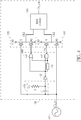
- FIG. 1 is a diagram illustrating a clock buffer 100 according to a first embodiment of the present invention.
- the clock buffer 100 comprises a first circuit (in this embodiment, the first circuit is an inverter 110), a second circuit (in this embodiment, the second circuit is an inverter 120) and an edge collector 130.
- the inverter 110 comprises a PMOS MP1 and an NMOS MN1, wherein a source electrode of the PMOS MP1 is coupled to a supply voltage VDD, a drain electrode of the PMOS MP1 is coupled to a drain electrode of the NMOS MN1, a source electrode of the NMOS MN1 is coupled to a ground voltage, and a size of the NMOS MN1 is greater than a size of the PMOS MP1.
- the inverter 120 comprises a PMOS MP2 and an NMOS MN2, wherein a source electrode of the PMOS MP2 is coupled to the supply voltage VDD, a drain electrode of the PMOS MP2 is coupled to a drain electrode of the NMOS MN2, a source electrode of the NMOS MN2 is coupled to the ground voltage, and a size of the PMOS MP2 is greater than a size of the NMOS MN2.
- the clock buffer 100 is configured to receive an input clock signal CK_in to generate an output clock signal CK_out, wherein the input clock signal CK_in is generated from a crystal oscillator (XO oscillator) 102.
- the inverter 110 receives the input clock signal CK_in to generate a first clock signal CK1
- the inverter 120 receives the input clock signal CK_in to generate a second clock signal CK2
- the edge collector 130 generates the output clock signal CK_out by using a falling edge of the first clock signal CK1 and a rising edge of the second clock signal CK2.
- the PMOS MP1 of the inverter 110 and the NMOS MN2 of the inverter 120 have small size, the static currents of the inverter 110 and the inverter 120 are much smaller than the conventional clock buffer, therefore, this skew design of the inverter 110 and the inverter 120 can significantly reduce the current consumption of the clock buffer 100 and mitigate the spur leakage.
- the PMOS MP1 of the inverter 110 has smaller size, the rising edge of the first clock signal CK1 may not good enough for the high performance applications, so only the falling edge of the first clock signal CK1 is used to generate the output clock signal CK_out.
- the clock buffer 100 can generate the output clock signal CK_out having better edges (i.e. less drift and phase noise) with lower power consumption.
- FIG. 2 shows a clock buffer 200 according to a second embodiment of the present invention. As shown in FIG.
- the clock buffer 200 comprises a first circuit (in this embodiment, the first circuit is an inverter 210), a second circuit (in this embodiment, the second circuit is an inverter 220), an edge collector 230, a first logical circuit 240, a first high-pass filter 250, a second logical circuit 260 and a second high-pass filter 270.
- the inverter 210 comprises a PMOS MP1 and an NMOS MN1, wherein a source electrode of the PMOS MP1 is coupled to a supply voltage VDD, a drain electrode of the PMOS MP1 is coupled to a drain electrode of the NMOS MN1, a source electrode of the NMOS MN1 is coupled to a ground voltage.
- the inverter 220 comprises a PMOS MP2 and an NMOS MN2, wherein a source electrode of the PMOS MP2 is coupled to the supply voltage VDD, a drain electrode of the PMOS MP2 is coupled to a drain electrode of the NMOS MN2, a source electrode of the NMOS MN2 is coupled to the ground voltage.
- the first logical circuit 240 comprises an inverter 242, a delay circuit 244 and an NAND gate 246.
- the high pass filter 250 comprises a capacitor C1 and a resistor R1 coupled to a bias voltage Vb1.
- the second logical circuit 260 comprises an inverter 262, a delay circuit 264 and a NOR gate 266.
- the high pass filter 270 comprises a capacitor C2 and a resistor R2 coupled to a bias voltage Vb2.
- the clock buffer 200 is configured to receive an input clock signal CK_in to generate an output clock signal CK_out, wherein the input clock signal CK_in is generated from a crystal oscillator 202.
- a size of the NMOS MN1 is greater than a size of the PMOS MP1
- a size of the PMOS MP2 is greater than a size of the NMOS MN2, but it's not a limitation of the present invention.
- the high pass-filter 250 filters the input clock signal CK_in to cause a negative phase shift, and the logical circuit 240 delays the input clock signal CK_in (filtered input clock signal) to generate a signal Vx to the PMOS MP1, and the PMOS MP1 and the NMOS MN1 receive the signal Vx and the input clock signal CK_in, respectively, to generate a first clock signal CK1.
- the high pass-filter 270 filters the input clock signal CK_in to cause a negative phase shift
- the logical circuit 260 delays the input clock signal CK_in (filtered input clock signal) to generate a signal to the NMOS MN2
- the PMOS MP2 and the NMOS MN2 receive the input clock signal CK_in and the signal outputted by the logical circuit 260, respectively, to generate a second clock signal CK2.
- the edge collector 230 generates the output clock signal CK_out by using a falling edge of the first clock signal CK1 and a rising edge of the second clock signal CK2.
- the time when the PMOS MP1 is turned on is delayed to avoid turning on the PMOS MP1 and the NMOS MN1 of the inverter 210 at the same time.
- the time when the NMOS MN2 is turned on is delayed to avoid turning on the PMOS MP2 and the NMOS MN2 of the inverter 220 at the same time.
- FIG. 3 shows the timing diagram of the signals related to the inverter 210 of the clock buffer 200, the symbol CK' is an output of the inverter 242, the symbol CK" is an output of the delay circuit 244, the symbol ⁇ is a phase shift provided by the high-pass filter 250, the symbol ⁇ t is a delay amount of the delay circuit 244.
- the signal Vx for turning on the PMOS MP1 is not overlapped with the period that the NMOS MN1 is turned on, the static current of the inverter 210 can be greatly reduced to improve the power consumption.
- the clock buffer 200 can generate the output clock signal CK_out having better edges with lower power consumption.
- the high-pass filter 250 is used to provide the negative phase shift to control the delay amount of the signal inputted into the PMOS MP1 (the bias voltage Vb1 allows fine adjustment)
- the high-pass filter 270 is used to provide the negative phase shift to control the delay amount of the signal inputted into the NMOS MN2 (the bias voltage Vb1 allows fine adjustment)
- the overall delay control can be simplified by using the high-pass filters 250 and 270.
- the high-pass filters 250 and 270 can be removed from the clock buffer 200, this alternative design shall fall within the scope of the present invention.
- FIG. 4 shows a clock buffer 400 according to a third embodiment of the present invention.
- the clock buffer 400 comprises a first circuit (in this embodiment, the first circuit is an inverter 41 0), a second circuit (in this embodiment, the second circuit is an inverter 420), an edge collector 430, a logical circuit 440 and a high-pass filter 450.
- the inverter 410 comprises a PMOS MP1 and an NMOS MN1, wherein a source electrode of the PMOS MP1 is coupled to a supply voltage VDD, a drain electrode of the PMOS MP1 is coupled to a drain electrode of the NMOS MN1, a source electrode of the NMOS MN1 is coupled to a ground voltage.
- the inverter 420 comprises a PMOS MP2 and an NMOS MN2, wherein a source electrode of the PMOS MP2 is coupled to the supply voltage VDD, a drain electrode of the PMOS MP2 is coupled to a drain electrode of the NMOS MN2, a source electrode of the NMOS MN2 is coupled to the ground voltage.
- the first logical circuit 440 comprises an inverter 442, a delay circuit 444, a NOR gate 446 and an NAND gate 448.
- the high-pass filter 450 comprises a capacitor C and a resistor R coupled to a bias voltage Vb.
- the clock buffer 400 is configured to receive an input clock signal CK_in to generate an output clock signal CK_out, wherein the input clock signal CK_in is generated from a crystal oscillator 402.
- a size of the NMOS MN1 is greater than a size of the PMOS MP1
- a size of the PMOS MP2 is greater than a size of the NMOS MN2, but it's not a limitation of the present invention.
- the high pass-filter 450 filters the input clock signal CK_in to cause a negative phase shift, and the logical circuit 440 delays the input clock signal CK_in (filtered input clock signal) to generate signals the PMOS MP1 and the NMOS MN2, respectively. Then, the PMOS MP1 and the NMOS MN1 of the inverter 410 receive the signal from the logical circuit 440 and the input clock signal CK_in to generate a first clock signal CK1, and the PMOS MP2 and the NMOS MN2 of the inverter 420 receive the input clock signal CK_in and the signal outputted by the logical circuit 440 to generate a second clock signal CK2.
- the edge collector 430 generates the output clock signal CK_out by using a falling edge of the first clock signal CK1 and a rising edge of the second clock signal CK2.
- the edge collector 430 because of the high-pass filter 450 and the logical circuit 440, the time when the PMOS MP1 is turned on is delayed to avoid turning on the PMOS MP1 and the NMOS MN1 of the inverter 410 at the same time, and the time when the NMOS MN2 is turned on is delayed to avoid turning on the PMOS MP2 and the NMOS MN2 of the inverter 420 at the same time. Therefore, the static currents of the inverter 410 and 420 can be greatly reduced to improve the power consumption.
- the clock buffer 400 is similar to the clock buffer 200 shown in FIG. 2 , and the difference is that the logical circuits 240 and 260 and the high-pass filters 250 and 270 shown in FIG. 2 are integrated and modified to be the logical circuit 440 and the high-pass filter 450, in order to save the chip area.
- the rising edge of the first clock signal CK1 and the falling edge of the second clock signal CK2 may have phase noise and larger transition time. Therefore, the rising edge of the first clock signal CK1 and the falling edge of the second clock signal CK2 are regarded as the unwanted edge, and the falling edge of the first clock signal CK1 and the rising edge of the second clock signal CK2 are regarded as the wanted edge, as shown in FIG. 5 , for the edge collector 130/230/430 to generate the output clock signal CK_out.
- FIG. 6 is a diagram illustrating an edge collector 600 according to one embodiment of the present invention, wherein the edge collector 600 can be any one of the edge collector 130, 230 and 430.
- the edge collector 600 comprises an inverter 610, a delay circuit 620, a NOR gate 630 and a D-type flip-flop (DFF).
- DFF D-type flip-flop
- the inverter 610 receives the second clock signal CK2 to generate an inverted second clock signal
- the NOR gate 630 receives the inverted second clock signal and the first clock signal CK1 to generate an NOR output
- the delay circuit 620 delays the inverted second clock signal CK2_B
- the DFF 640 uses the NOR output to sample the output of the delay circuit 620 to generate the output clock signal CK_out.
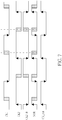
- FIG. 7 shows a timing diagram of the signals shown in FIG. 6 .
- the first clock signal CK1 and the second clock signal CK2 shown in FIG. 2 and FIG. 4 may become unbalance due to the logical circuits in front of the inverters, for example, the first clock signal CK1 may have the duty cycle less than 50%, and the second clock signal may have the duty cycle greater than 50% shown in FIG. 7 .
- the output clock signal CK_out has the balanced duty cycle, and is more suitable for use in the following circuits.
- FIG. 8 is a diagram illustrating an edge collector 800 according to another embodiment of the preset invention.
- the edge collector 800 comprises an inverter 810, a latch circuit comprising two NAND gates 820 and 830, and a multiplexer 840.
- the inverter 810 receives the first clock signal CK1 to generate an inverted first clock signal
- the latch circuit receives the inverted first clock signal and the second clock signal CK2 to generate a selection signal SEL to control the multiplexer 840 to output one of the first clock signal CK1 and the second clock signal CK2.
- FIG. 9 shows a timing diagram of the signals shown in FIG. 8 .
- edge collectors 800 and 600 are for illustrative purposes only, that is the detailed circuit structures edge collectors 800 and 600 are not limitations of the present invention.
- the clock buffer has a first circuit and a second circuit for receiving the input clock signal to generate a first clock signal and a second clock signal, respectively, wherein the first clock signal may have a better falling edge and worse rising edge, and the second clock signal may have a better rising edge and worse falling edge due to the circuit design for the power consumption.
- the clock buffer further uses an edge collector to use the better falling edge of the first clock signal and the better rising edge of the second clock signal to generate the output clock signal. Therefore, the clock buffer has lower power consumption and is able to generate the output clock signal with higher quality, and the spur leakage is improved by removing the static current.
Landscapes
- Engineering & Computer Science (AREA)
- Physics & Mathematics (AREA)
- Computer Hardware Design (AREA)
- General Engineering & Computer Science (AREA)
- Computing Systems (AREA)
- Mathematical Physics (AREA)
- Theoretical Computer Science (AREA)
- General Physics & Mathematics (AREA)
- Nonlinear Science (AREA)
- Manipulation Of Pulses (AREA)
- Logic Circuits (AREA)
Abstract
Description
- This application claims the priority of
US Provisional Application No. 62/741,006, filed on October 4th, 2018 - A conventional clock buffer is generally implemented by an inverter whose N-type Metal-Oxide-Semiconductor (NMOS) and P-type MOS (PMOS) are generally designed larger for better noise performance. However, because of the rising/falling time, the NMOS and the PMOS are both turned on for a long duration, and a static current generated in this duration can dominate a power consumption of the clock signal and cause a spur to affect the other circuits, wherein the static current is greater if the NMOS and the PMOS have larger size. To solve this problem,
US Patent US8,427,209 provides a delay circuit in front of the PMOS to control the turn-on period of the PMOS to lower the power consumption, however, this method will shorten a duty cycle of an output clock signal, and the edge of the output clock signal may be drifted to worsen the phase noise. - It is therefore an objective of the present invention to provide a clock buffer which has lower power consumption, and the output clock signal generated by the clock buffer has better edges and duty cycle, to solve the above-mentioned problems.
- In one embodiment of the present invention, a clock buffer comprises a first circuit, a second circuit and an edge collector, wherein the first circuit is arranged to receive an input clock signal to generate a first clock signal, the second circuit is arranged to receive the input clock signal to generate a second clock signal, and the edge collector is arranged to generate an output clock signal by using a falling edge of the first clock signal and a rising edge of the second clock signal.
- These and other objectives of the present invention will no doubt become obvious to those of ordinary skill in the art after reading the following detailed description of the preferred embodiment that is illustrated in the various figures and drawings.
-
-
FIG. 1 is a diagram illustrating a clock buffer according to a first embodiment of the present invention. -
FIG. 2 is a diagram illustrating a clock buffer according to a second embodiment of the present invention. -
FIG. 3 shows the timing diagram of the signals related to the inverter shown inFIG. 2 -
FIG. 4 is a diagram illustrating a clock buffer according to a third embodiment of the present invention. -
FIG. 5 shows edges of the first clock signal and the second clock signal. -
FIG. 6 is a diagram illustrating an edge collector according to one embodiment of the present invention. -
FIG. 7 shows a timing diagram of the signals shown inFIG. 6 . -
FIG. 8 is a diagram illustrating an edge collector according to another embodiment of the present invention. -
FIG. 9 shows a timing diagram of the signals shown inFIG. 8 . - Certain terms are used throughout the following description and claims to refer to particular system components. As one skilled in the art will appreciate, manufacturers may refer to a component by different names. This document does not intend to distinguish between components that differ in name but not function. In the following discussion and in the claims, the terms "including" and "comprising" are used in an open-ended fashion, and thus should be interpreted to mean "including, but not limited to ...". The terms "couple" and "couples" are intended to mean either an indirect or a direct electrical connection. Thus, if a first device couples to a second device, that connection may be through a direct electrical connection, or through an indirect electrical connection via other devices and connections.
-
FIG. 1 is a diagram illustrating aclock buffer 100 according to a first embodiment of the present invention. As shown inFIG. 1 , theclock buffer 100 comprises a first circuit (in this embodiment, the first circuit is an inverter 110), a second circuit (in this embodiment, the second circuit is an inverter 120) and anedge collector 130. Theinverter 110 comprises a PMOS MP1 and an NMOS MN1, wherein a source electrode of the PMOS MP1 is coupled to a supply voltage VDD, a drain electrode of the PMOS MP1 is coupled to a drain electrode of the NMOS MN1, a source electrode of the NMOS MN1 is coupled to a ground voltage, and a size of the NMOS MN1 is greater than a size of the PMOS MP1. Theinverter 120 comprises a PMOS MP2 and an NMOS MN2, wherein a source electrode of the PMOS MP2 is coupled to the supply voltage VDD, a drain electrode of the PMOS MP2 is coupled to a drain electrode of the NMOS MN2, a source electrode of the NMOS MN2 is coupled to the ground voltage, and a size of the PMOS MP2 is greater than a size of the NMOS MN2. In this embodiment, theclock buffer 100 is configured to receive an input clock signal CK_in to generate an output clock signal CK_out, wherein the input clock signal CK_in is generated from a crystal oscillator (XO oscillator) 102. - In the operations of the
clock buffer 100, theinverter 110 receives the input clock signal CK_in to generate a first clock signal CK1, theinverter 120 receives the input clock signal CK_in to generate a second clock signal CK2, and theedge collector 130 generates the output clock signal CK_out by using a falling edge of the first clock signal CK1 and a rising edge of the second clock signal CK2. In this embodiment, because the PMOS MP1 of theinverter 110 and the NMOS MN2 of theinverter 120 have small size, the static currents of theinverter 110 and theinverter 120 are much smaller than the conventional clock buffer, therefore, this skew design of theinverter 110 and theinverter 120 can significantly reduce the current consumption of theclock buffer 100 and mitigate the spur leakage. In addition, because the PMOS MP1 of theinverter 110 has smaller size, the rising edge of the first clock signal CK1 may not good enough for the high performance applications, so only the falling edge of the first clock signal CK1 is used to generate the output clock signal CK_out. Similarly, because the NMOS MN2 of theinverter 120 has smaller size, the falling edge of the second clock signal CK2 may not good enough for the high performance applications, so only the rising edge of the second clock signal CK2 is used to generate the output clock signal CK_out. In light of above, theclock buffer 100 can generate the output clock signal CK_out having better edges (i.e. less drift and phase noise) with lower power consumption. - In the embodiment shown in
FIG. 1 , although the power consumption of theclock buffer 100 is better than the conventional art, the PMOS MP1 and the NMOS MN1 of theinverter 110 still have time to be turned on at the same time, the PMOS MP2 and the NMOS MN2 of theinverter 120 still have time to be turned on at the same time, and the static current is generated accordingly. Therefore, in order to further reduce the power consumption, other circuits may be positioned between the input clock signal CK_in and theinverters 110/120 to avoid turning on the PMOS and NMOS at the same time.FIG. 2 shows aclock buffer 200 according to a second embodiment of the present invention. As shown inFIG. 2 , theclock buffer 200 comprises a first circuit (in this embodiment, the first circuit is an inverter 210), a second circuit (in this embodiment, the second circuit is an inverter 220), anedge collector 230, a firstlogical circuit 240, a first high-pass filter 250, a secondlogical circuit 260 and a second high-pass filter 270. Theinverter 210 comprises a PMOS MP1 and an NMOS MN1, wherein a source electrode of the PMOS MP1 is coupled to a supply voltage VDD, a drain electrode of the PMOS MP1 is coupled to a drain electrode of the NMOS MN1, a source electrode of the NMOS MN1 is coupled to a ground voltage. Theinverter 220 comprises a PMOS MP2 and an NMOS MN2, wherein a source electrode of the PMOS MP2 is coupled to the supply voltage VDD, a drain electrode of the PMOS MP2 is coupled to a drain electrode of the NMOS MN2, a source electrode of the NMOS MN2 is coupled to the ground voltage. The firstlogical circuit 240 comprises aninverter 242, adelay circuit 244 and anNAND gate 246. Thehigh pass filter 250 comprises a capacitor C1 and a resistor R1 coupled to a bias voltage Vb1. The secondlogical circuit 260 comprises aninverter 262, adelay circuit 264 and aNOR gate 266. Thehigh pass filter 270 comprises a capacitor C2 and a resistor R2 coupled to a bias voltage Vb2. In this embodiment, theclock buffer 200 is configured to receive an input clock signal CK_in to generate an output clock signal CK_out, wherein the input clock signal CK_in is generated from acrystal oscillator 202. - In this embodiment, a size of the NMOS MN1 is greater than a size of the PMOS MP1, and a size of the PMOS MP2 is greater than a size of the NMOS MN2, but it's not a limitation of the present invention.
- In the operations of the
clock buffer 200, the high pass-filter 250 filters the input clock signal CK_in to cause a negative phase shift, and thelogical circuit 240 delays the input clock signal CK_in (filtered input clock signal) to generate a signal Vx to the PMOS MP1, and the PMOS MP1 and the NMOS MN1 receive the signal Vx and the input clock signal CK_in, respectively, to generate a first clock signal CK1. Similarly, the high pass-filter 270 filters the input clock signal CK_in to cause a negative phase shift, and thelogical circuit 260 delays the input clock signal CK_in (filtered input clock signal) to generate a signal to the NMOS MN2, and the PMOS MP2 and the NMOS MN2 receive the input clock signal CK_in and the signal outputted by thelogical circuit 260, respectively, to generate a second clock signal CK2. Then, theedge collector 230 generates the output clock signal CK_out by using a falling edge of the first clock signal CK1 and a rising edge of the second clock signal CK2. In this embodiment, because of the high-pass filter 250 and thelogical circuit 240, the time when the PMOS MP1 is turned on is delayed to avoid turning on the PMOS MP1 and the NMOS MN1 of theinverter 210 at the same time. Similarly, because of the high-pass filter 270 and thelogical circuit 260, the time when the NMOS MN2 is turned on is delayed to avoid turning on the PMOS MP2 and the NMOS MN2 of theinverter 220 at the same time.FIG. 3 shows the timing diagram of the signals related to theinverter 210 of theclock buffer 200, the symbol CK' is an output of theinverter 242, the symbol CK" is an output of thedelay circuit 244, the symbol Φ is a phase shift provided by the high-pass filter 250, the symbol Δt is a delay amount of thedelay circuit 244. As shown inFIG. 3 , because the signal Vx for turning on the PMOS MP1 is not overlapped with the period that the NMOS MN1 is turned on, the static current of theinverter 210 can be greatly reduced to improve the power consumption. - In this embodiment, because the high-
pass filter 250 and thelogical circuit 240 is coupled between the input clock signal CK_in and theinverter 210, the rising edge of the first clock signal CK1 may not good enough for the high performance applications, so only the falling edge of the first clock signal CK1 is used to generate the output clock signal CK_out. Similarly, because the high-pass filter 270 and thelogical circuit 260 is coupled between the input clock signal CK_in and theinverter 220, the falling edge of the second clock signal CK2 may not good enough for the high performance applications, so only the rising edge of the second clock signal CK2 is used to generate the output clock signal CK_out. In light of above, theclock buffer 200 can generate the output clock signal CK_out having better edges with lower power consumption. - In this embodiment, the high-
pass filter 250 is used to provide the negative phase shift to control the delay amount of the signal inputted into the PMOS MP1 (the bias voltage Vb1 allows fine adjustment), and the high-pass filter 270 is used to provide the negative phase shift to control the delay amount of the signal inputted into the NMOS MN2 (the bias voltage Vb1 allows fine adjustment), and the overall delay control can be simplified by using the high-pass filters pass filters clock buffer 200, this alternative design shall fall within the scope of the present invention. -
FIG. 4 shows aclock buffer 400 according to a third embodiment of the present invention. As shown inFIG. 4 , theclock buffer 400 comprises a first circuit (in this embodiment, the first circuit is an inverter 41 0), a second circuit (in this embodiment, the second circuit is an inverter 420), anedge collector 430, alogical circuit 440 and a high-pass filter 450. Theinverter 410 comprises a PMOS MP1 and an NMOS MN1, wherein a source electrode of the PMOS MP1 is coupled to a supply voltage VDD, a drain electrode of the PMOS MP1 is coupled to a drain electrode of the NMOS MN1, a source electrode of the NMOS MN1 is coupled to a ground voltage. Theinverter 420 comprises a PMOS MP2 and an NMOS MN2, wherein a source electrode of the PMOS MP2 is coupled to the supply voltage VDD, a drain electrode of the PMOS MP2 is coupled to a drain electrode of the NMOS MN2, a source electrode of the NMOS MN2 is coupled to the ground voltage. The firstlogical circuit 440 comprises aninverter 442, adelay circuit 444, aNOR gate 446 and anNAND gate 448. The high-pass filter 450 comprises a capacitor C and a resistor R coupled to a bias voltage Vb. In this embodiment, theclock buffer 400 is configured to receive an input clock signal CK_in to generate an output clock signal CK_out, wherein the input clock signal CK_in is generated from acrystal oscillator 402. - In this embodiment, a size of the NMOS MN1 is greater than a size of the PMOS MP1, and a size of the PMOS MP2 is greater than a size of the NMOS MN2, but it's not a limitation of the present invention.
- In the operations of the
clock buffer 400, the high pass-filter 450 filters the input clock signal CK_in to cause a negative phase shift, and thelogical circuit 440 delays the input clock signal CK_in (filtered input clock signal) to generate signals the PMOS MP1 and the NMOS MN2, respectively. Then, the PMOS MP1 and the NMOS MN1 of theinverter 410 receive the signal from thelogical circuit 440 and the input clock signal CK_in to generate a first clock signal CK1, and the PMOS MP2 and the NMOS MN2 of theinverter 420 receive the input clock signal CK_in and the signal outputted by thelogical circuit 440 to generate a second clock signal CK2. Then, theedge collector 430 generates the output clock signal CK_out by using a falling edge of the first clock signal CK1 and a rising edge of the second clock signal CK2. In this embodiment, because of the high-pass filter 450 and thelogical circuit 440, the time when the PMOS MP1 is turned on is delayed to avoid turning on the PMOS MP1 and the NMOS MN1 of theinverter 410 at the same time, and the time when the NMOS MN2 is turned on is delayed to avoid turning on the PMOS MP2 and the NMOS MN2 of theinverter 420 at the same time. Therefore, the static currents of theinverter - The
clock buffer 400 is similar to theclock buffer 200 shown inFIG. 2 , and the difference is that thelogical circuits pass filters FIG. 2 are integrated and modified to be thelogical circuit 440 and the high-pass filter 450, in order to save the chip area. - In the embodiments, because of the skew design of the
inverters FIG. 1 , thelogical circuits FIG. 2 and thelogical circuit 440 shown inFIG. 4 , the rising edge of the first clock signal CK1 and the falling edge of the second clock signal CK2 may have phase noise and larger transition time. Therefore, the rising edge of the first clock signal CK1 and the falling edge of the second clock signal CK2 are regarded as the unwanted edge, and the falling edge of the first clock signal CK1 and the rising edge of the second clock signal CK2 are regarded as the wanted edge, as shown inFIG. 5 , for theedge collector 130/230/430 to generate the output clock signal CK_out. -
FIG. 6 is a diagram illustrating anedge collector 600 according to one embodiment of the present invention, wherein theedge collector 600 can be any one of theedge collector FIG. 6 , theedge collector 600 comprises aninverter 610, adelay circuit 620, a NORgate 630 and a D-type flip-flop (DFF). In the operations of theedge collector 600, theinverter 610 receives the second clock signal CK2 to generate an inverted second clock signal, the NORgate 630 receives the inverted second clock signal and the first clock signal CK1 to generate an NOR output, thedelay circuit 620 delays the inverted second clock signal CK2_B, and theDFF 640 uses the NOR output to sample the output of thedelay circuit 620 to generate the output clock signal CK_out.FIG. 7 shows a timing diagram of the signals shown inFIG. 6 . - In addition, if the input clock signal CK_in has the duty cycle 50%, the first clock signal CK1 and the second clock signal CK2 shown in
FIG. 2 andFIG. 4 may become unbalance due to the logical circuits in front of the inverters, for example, the first clock signal CK1 may have the duty cycle less than 50%, and the second clock signal may have the duty cycle greater than 50% shown inFIG. 7 . By using theedge collector 600, the output clock signal CK_out has the balanced duty cycle, and is more suitable for use in the following circuits. -
FIG. 8 is a diagram illustrating anedge collector 800 according to another embodiment of the preset invention. InFIG. 8 , theedge collector 800 comprises aninverter 810, a latch circuit comprising twoNAND gates multiplexer 840. In the operations of theedge collector 800, theinverter 810 receives the first clock signal CK1 to generate an inverted first clock signal, and the latch circuit receives the inverted first clock signal and the second clock signal CK2 to generate a selection signal SEL to control themultiplexer 840 to output one of the first clock signal CK1 and the second clock signal CK2.FIG. 9 shows a timing diagram of the signals shown inFIG. 8 . - It is noted that the
edge collectors collectors - Briefly summarized, in the clock buffer of the present invention, the clock buffer has a first circuit and a second circuit for receiving the input clock signal to generate a first clock signal and a second clock signal, respectively, wherein the first clock signal may have a better falling edge and worse rising edge, and the second clock signal may have a better rising edge and worse falling edge due to the circuit design for the power consumption. Then, the clock buffer further uses an edge collector to use the better falling edge of the first clock signal and the better rising edge of the second clock signal to generate the output clock signal. Therefore, the clock buffer has lower power consumption and is able to generate the output clock signal with higher quality, and the spur leakage is improved by removing the static current.
- Those skilled in the art will readily observe that numerous modifications and alterations of the device and method may be made while retaining the teachings of the invention. Accordingly, the above disclosure should be construed as limited only by the metes and bounds of the appended claims.
Claims (12)
- A clock buffer (100, 200, 400), comprising:a first circuit (110, 210, 410), for receiving an input clock signal to generate a first clock signal;a second circuit (120, 220, 420), for receiving the input clock signal to generate a second clock signal; andan edge collector (1 30, 230, 430, 600, 800), coupled to the first circuit (1 10, 210, 410) and the second circuit (120, 220, 420), for generating an output clock signal by using a falling edge of the first clock signal and a rising edge of the second clock signal.
- The clock buffer (100, 200, 400) of claim 1, wherein the edge collector (130, 230, 430, 600, 800) does not use a rising edge of the first clock signal and a falling edge of the second clock signal to generate the output clock signal.
- The clock buffer (100, 200, 400) of claim 1, wherein the first circuit (110, 210, 410) comprises:a first P-type transistor, wherein a source electrode of the first P-type transistor is coupled to a first reference voltage, and the input clock signal is inputted into a gate electrode of the first P-type transistor; anda first N-type transistor, wherein a source electrode of the first N-type transistor is coupled to a second reference voltage, a drain electrode of the first N-type transistor is coupled to a drain electrode of the first P-type transistor for outputting the first clock signal, and the input clock signal is inputted into a gate electrode of the first N-type transistor;wherein a size of the first N-type transistor is larger than a size of the first P-type transistor.
- The clock buffer (100, 200, 400) of claim 3, wherein the second circuit (120, 220, 420) comprises:a second P-type transistor, wherein a source electrode of the second P-type transistor is coupled to the first reference voltage, and the input clock signal is inputted into a gate electrode of the second P-type transistor; anda second N-type transistor, wherein a source electrode of the second N-type transistor is coupled to the second reference voltage, a drain electrode of the second N-type transistor is coupled to a drain electrode of the second P-type transistor for outputting the second clock signal, and the input clock signal is inputted into a gate electrode of the second N-type transistor;wherein a size of the second P-type transistor is larger than a size of the second N-type transistor.
- The clock buffer (100, 200, 400) of claim 1, wherein the first circuit (110, 210, 410) comprises:a first P-type transistor, wherein a source electrode of the first P-type transistor is coupled to a first reference voltage;a first logical circuit, for generating a first delayed input clock signal to a gate electrode of the first P-type transistor according to the input clock signal; anda first N-type transistor, wherein a source electrode of the first N-type transistor is coupled to a second reference voltage, a drain electrode of the first N-type transistor is coupled to a drain electrode of the first P-type transistor for outputting the first clock signal, and the input clock signal is inputted into a gate electrode of the first N-type transistor;
- The clock buffer (100, 200, 400) of claim 5, wherein a size of the first N-type transistor is larger than a size of the first P-type transistor.
- The clock buffer (100, 200, 400) of claim 5, wherein the first circuit (110, 210, 410) further comprises:
a first high-pass filter, coupled between the first logical circuit and the input clock signal. - The clock buffer (100, 200, 400) of claim 5, wherein the second circuit (120, 220, 420) comprises:a second P-type transistor, wherein a source electrode of the second P-type transistor is coupled to the first reference voltage, and the input clock signal is inputted into a gate electrode of the second P-type transistor; anda second N-type transistor, wherein a source electrode of the second N-type transistor is coupled to the second reference voltage, a drain electrode of the second N-type transistor is coupled to a drain electrode of the second P-type transistor for outputting the second clock signal; anda second logical circuit, for generating a second delayed input clock signal to a gate electrode of the second N-type transistor according to the input clock signal.
- The clock buffer (100, 200, 400) of claim 8, wherein a size of the second P-type transistor is larger than a size of the second N-type transistor.
- The clock buffer (100, 200, 400) of claim 8, wherein the second circuit (120, 220, 420) further comprises:
a second high-pass filter, coupled between the second logical circuit and the input clock signal. - The clock buffer (100, 200, 400) of claim 1, wherein the first circuit (110, 210, 410) comprises:a first P-type transistor, wherein a source electrode of the first P-type transistor is coupled to a first reference voltage, and the input clock signal is inputted into a gate electrode of the first P-type transistor; anda first N-type transistor, wherein a source electrode of the first N-type transistor is coupled to a second reference voltage, a drain electrode of the first N-type transistor is coupled to a drain electrode of the first P-type transistor for outputting the first clock signal; andthe second circuit (120, 220, 420) comprises:a second P-type transistor, wherein a source electrode of the second P-type transistor is coupled to the first reference voltage; anda second N-type transistor, wherein a source electrode of the second N-type transistor is coupled to the second reference voltage, a drain electrode of the second N-type transistor is coupled to a drain electrode of the second P-type transistor for outputting the second clock signal, and the input clock signal is inputted into a gate electrode of the second N-type transistor; andthe clock buffer (100, 200, 400) further comprises:
a logical circuit, for generating a first delayed clock signal and a second delayed clock signal according to the input clock signal, wherein the first delayed clock signal is inputted into a gate electrode of the first P-type transistor, and the second delayed clock signal is inputted into a gate electrode of the second N-type transistor. - The clock buffer (100, 200, 400) of claim 11, further comprising:
a high-pass filter, coupled between the logical circuit and the input clock signal.
Applications Claiming Priority (2)
| Application Number | Priority Date | Filing Date | Title |
|---|---|---|---|
| US201862741006P | 2018-10-04 | 2018-10-04 | |
| US16/553,163 US10809757B2 (en) | 2018-10-04 | 2019-08-27 | Clock buffer having low power, low noise and low spur |
Publications (2)
| Publication Number | Publication Date |
|---|---|
| EP3633855A1 true EP3633855A1 (en) | 2020-04-08 |
| EP3633855B1 EP3633855B1 (en) | 2024-09-11 |
Family
ID=68066725
Family Applications (1)
| Application Number | Title | Priority Date | Filing Date |
|---|---|---|---|
| EP19199448.2A Active EP3633855B1 (en) | 2018-10-04 | 2019-09-25 | Clock buffer having low power, low noise and low spur |
Country Status (4)
| Country | Link |
|---|---|
| US (1) | US10809757B2 (en) |
| EP (1) | EP3633855B1 (en) |
| CN (1) | CN111010165B (en) |
| TW (1) | TWI698089B (en) |
Citations (4)
| Publication number | Priority date | Publication date | Assignee | Title |
|---|---|---|---|---|
| US6025738A (en) * | 1997-08-22 | 2000-02-15 | International Business Machines Corporation | Gain enhanced split drive buffer |
| US20010025913A1 (en) * | 2000-02-04 | 2001-10-04 | Takashi Tanimoto | Drive apparatus for CCD image sensor |
| EP1271285A2 (en) * | 2001-06-29 | 2003-01-02 | Fujitsu Limited | Low latency clock distribution |
| US8427209B2 (en) | 2010-12-20 | 2013-04-23 | National Semiconductor Corporation | Sampling phase lock loop (PLL) with low power clock buffer |
Family Cites Families (9)
| Publication number | Priority date | Publication date | Assignee | Title |
|---|---|---|---|---|
| DE4231175C1 (en) * | 1992-09-17 | 1994-01-13 | Siemens Ag | Arrangement for clock recovery |
| US5610548A (en) * | 1995-09-08 | 1997-03-11 | International Business Machines Corporation | Split drive clock buffer |
| US6094086A (en) | 1997-05-12 | 2000-07-25 | Industrial Technology Research Institute | High drive CMOS output buffer with fast and slow speed controls |
| US6040713A (en) | 1998-04-22 | 2000-03-21 | Micron Technology, Inc. | Buffer with fast edge propagation |
| US6310499B1 (en) * | 2000-07-17 | 2001-10-30 | Hewlett-Packard Company | Methods and apparatus for adjusting the deadtime between non-overlapping clock signals |
| KR100894984B1 (en) | 2003-01-20 | 2009-04-24 | 삼성전자주식회사 | Synchronous output buffer, synchronous memory device and access time measurement method |
| GB2459451A (en) * | 2008-04-22 | 2009-10-28 | Sharp Kk | A scan pulse shift register for an active matrix display |
| US7924066B2 (en) | 2009-03-25 | 2011-04-12 | Fairchild Semiconductor Corporation | Low speed, load independent, slew rate controlled output buffer with no DC power consumption |
| US9473120B1 (en) * | 2015-05-18 | 2016-10-18 | Qualcomm Incorporated | High-speed AC-coupled inverter-based buffer with replica biasing |
-
2019
- 2019-08-27 US US16/553,163 patent/US10809757B2/en active Active
- 2019-09-19 CN CN201910886694.6A patent/CN111010165B/en active Active
- 2019-09-25 EP EP19199448.2A patent/EP3633855B1/en active Active
- 2019-10-02 TW TW108135712A patent/TWI698089B/en active
Patent Citations (4)
| Publication number | Priority date | Publication date | Assignee | Title |
|---|---|---|---|---|
| US6025738A (en) * | 1997-08-22 | 2000-02-15 | International Business Machines Corporation | Gain enhanced split drive buffer |
| US20010025913A1 (en) * | 2000-02-04 | 2001-10-04 | Takashi Tanimoto | Drive apparatus for CCD image sensor |
| EP1271285A2 (en) * | 2001-06-29 | 2003-01-02 | Fujitsu Limited | Low latency clock distribution |
| US8427209B2 (en) | 2010-12-20 | 2013-04-23 | National Semiconductor Corporation | Sampling phase lock loop (PLL) with low power clock buffer |
Also Published As
| Publication number | Publication date |
|---|---|
| TW202015335A (en) | 2020-04-16 |
| EP3633855B1 (en) | 2024-09-11 |
| CN111010165A (en) | 2020-04-14 |
| CN111010165B (en) | 2023-11-10 |
| US10809757B2 (en) | 2020-10-20 |
| US20200110435A1 (en) | 2020-04-09 |
| TWI698089B (en) | 2020-07-01 |
Similar Documents
| Publication | Publication Date | Title |
|---|---|---|
| JP3532153B2 (en) | Level shifter control circuit | |
| US20160118962A1 (en) | Signal generating system and signal generating method | |
| WO2018113668A1 (en) | Wide capture range reference-less frequency detector | |
| US20230006659A1 (en) | Duty-cycle corrector circuits and related apparatuses and methods | |
| CN112438021B (en) | High Speed Low Power Level Shift Clock Buffer | |
| US20170257080A1 (en) | Low-area low clock-power flip-flop | |
| US20080001628A1 (en) | Level conversion circuit | |
| US8138800B2 (en) | Phase detecting circuit and PLL circuit | |
| EP3633855B1 (en) | Clock buffer having low power, low noise and low spur | |
| US20160147252A1 (en) | Clock circuit and method of operating the same | |
| WO2022247681A1 (en) | Delay modulation circuit and method, chip, and server | |
| JP2005167804A (en) | Noise reduction circuit | |
| US7453294B1 (en) | Dynamic frequency divider with improved leakage tolerance | |
| US9742413B2 (en) | Electronic device and information processing apparatus | |
| JP2006211158A (en) | Semiconductor device provided with MOS transistor | |
| US11329639B1 (en) | Delay cell for quadrature clock generation with insensitivity to PVT variation and equal rising/falling edges | |
| US6900684B2 (en) | Pulse processing circuit and frequency multiplier circuit | |
| US7317345B2 (en) | Anti-gate leakage programmable capacitor | |
| US8344782B2 (en) | Method and apparatus to limit circuit delay dependence on voltage for single phase transition | |
| US20120169382A1 (en) | Dividing method and dividing apparatus for generating noise-reduced frequency divided signal by utilizing noise reducing circuit | |
| GB2473180A (en) | Voltage controlled oscillator with reduced noise | |
| US20160226469A1 (en) | Flip-flop devices with clock sharing | |
| JP2017050777A (en) | Output buffer circuit | |
| JP2000114939A (en) | Clock signal generating device | |
| CN115459750A (en) | Non-overlapping clock signal generating circuit |
Legal Events
| Date | Code | Title | Description |
|---|---|---|---|
| PUAI | Public reference made under article 153(3) epc to a published international application that has entered the european phase |
Free format text: ORIGINAL CODE: 0009012 |
|
| STAA | Information on the status of an ep patent application or granted ep patent |
Free format text: STATUS: THE APPLICATION HAS BEEN PUBLISHED |
|
| AK | Designated contracting states |
Kind code of ref document: A1 Designated state(s): AL AT BE BG CH CY CZ DE DK EE ES FI FR GB GR HR HU IE IS IT LI LT LU LV MC MK MT NL NO PL PT RO RS SE SI SK SM TR |
|
| AX | Request for extension of the european patent |
Extension state: BA ME |
|
| STAA | Information on the status of an ep patent application or granted ep patent |
Free format text: STATUS: REQUEST FOR EXAMINATION WAS MADE |
|
| 17P | Request for examination filed |
Effective date: 20200930 |
|
| RBV | Designated contracting states (corrected) |
Designated state(s): AL AT BE BG CH CY CZ DE DK EE ES FI FR GB GR HR HU IE IS IT LI LT LU LV MC MK MT NL NO PL PT RO RS SE SI SK SM TR |
|
| STAA | Information on the status of an ep patent application or granted ep patent |
Free format text: STATUS: EXAMINATION IS IN PROGRESS |
|
| 17Q | First examination report despatched |
Effective date: 20211201 |
|
| P01 | Opt-out of the competence of the unified patent court (upc) registered |
Effective date: 20230607 |
|
| GRAP | Despatch of communication of intention to grant a patent |
Free format text: ORIGINAL CODE: EPIDOSNIGR1 |
|
| STAA | Information on the status of an ep patent application or granted ep patent |
Free format text: STATUS: GRANT OF PATENT IS INTENDED |
|
| INTG | Intention to grant announced |
Effective date: 20240409 |
|
| GRAS | Grant fee paid |
Free format text: ORIGINAL CODE: EPIDOSNIGR3 |
|
| GRAA | (expected) grant |
Free format text: ORIGINAL CODE: 0009210 |
|
| STAA | Information on the status of an ep patent application or granted ep patent |
Free format text: STATUS: THE PATENT HAS BEEN GRANTED |
|
| AK | Designated contracting states |
Kind code of ref document: B1 Designated state(s): AL AT BE BG CH CY CZ DE DK EE ES FI FR GB GR HR HU IE IS IT LI LT LU LV MC MK MT NL NO PL PT RO RS SE SI SK SM TR |
|
| REG | Reference to a national code |
Ref country code: GB Ref legal event code: FG4D |
|
| RIN1 | Information on inventor provided before grant (corrected) |
Inventor name: HSUEH, YU-LI Inventor name: CHEN, CHIEN-WEI |
|
| REG | Reference to a national code |
Ref country code: CH Ref legal event code: EP |
|
| REG | Reference to a national code |
Ref country code: DE Ref legal event code: R096 Ref document number: 602019058612 Country of ref document: DE |
|
| REG | Reference to a national code |
Ref country code: IE Ref legal event code: FG4D |
|
| REG | Reference to a national code |
Ref country code: LT Ref legal event code: MG9D |
|
| PG25 | Lapsed in a contracting state [announced via postgrant information from national office to epo] |
Ref country code: NO Free format text: LAPSE BECAUSE OF FAILURE TO SUBMIT A TRANSLATION OF THE DESCRIPTION OR TO PAY THE FEE WITHIN THE PRESCRIBED TIME-LIMIT Effective date: 20241211 |
|
| REG | Reference to a national code |
Ref country code: NL Ref legal event code: MP Effective date: 20240911 |
|
| PG25 | Lapsed in a contracting state [announced via postgrant information from national office to epo] |
Ref country code: GR Free format text: LAPSE BECAUSE OF FAILURE TO SUBMIT A TRANSLATION OF THE DESCRIPTION OR TO PAY THE FEE WITHIN THE PRESCRIBED TIME-LIMIT Effective date: 20241212 Ref country code: FI Free format text: LAPSE BECAUSE OF FAILURE TO SUBMIT A TRANSLATION OF THE DESCRIPTION OR TO PAY THE FEE WITHIN THE PRESCRIBED TIME-LIMIT Effective date: 20240911 |
|
| PG25 | Lapsed in a contracting state [announced via postgrant information from national office to epo] |
Ref country code: BG Free format text: LAPSE BECAUSE OF FAILURE TO SUBMIT A TRANSLATION OF THE DESCRIPTION OR TO PAY THE FEE WITHIN THE PRESCRIBED TIME-LIMIT Effective date: 20240911 |
|
| PG25 | Lapsed in a contracting state [announced via postgrant information from national office to epo] |
Ref country code: LV Free format text: LAPSE BECAUSE OF FAILURE TO SUBMIT A TRANSLATION OF THE DESCRIPTION OR TO PAY THE FEE WITHIN THE PRESCRIBED TIME-LIMIT Effective date: 20240911 |
|
| PG25 | Lapsed in a contracting state [announced via postgrant information from national office to epo] |
Ref country code: HR Free format text: LAPSE BECAUSE OF FAILURE TO SUBMIT A TRANSLATION OF THE DESCRIPTION OR TO PAY THE FEE WITHIN THE PRESCRIBED TIME-LIMIT Effective date: 20240911 |
|
| PG25 | Lapsed in a contracting state [announced via postgrant information from national office to epo] |
Ref country code: ES Free format text: LAPSE BECAUSE OF FAILURE TO SUBMIT A TRANSLATION OF THE DESCRIPTION OR TO PAY THE FEE WITHIN THE PRESCRIBED TIME-LIMIT Effective date: 20240911 Ref country code: RS Free format text: LAPSE BECAUSE OF FAILURE TO SUBMIT A TRANSLATION OF THE DESCRIPTION OR TO PAY THE FEE WITHIN THE PRESCRIBED TIME-LIMIT Effective date: 20241211 |
|
| PG25 | Lapsed in a contracting state [announced via postgrant information from national office to epo] |
Ref country code: RS Free format text: LAPSE BECAUSE OF FAILURE TO SUBMIT A TRANSLATION OF THE DESCRIPTION OR TO PAY THE FEE WITHIN THE PRESCRIBED TIME-LIMIT Effective date: 20241211 Ref country code: NO Free format text: LAPSE BECAUSE OF FAILURE TO SUBMIT A TRANSLATION OF THE DESCRIPTION OR TO PAY THE FEE WITHIN THE PRESCRIBED TIME-LIMIT Effective date: 20241211 Ref country code: LV Free format text: LAPSE BECAUSE OF FAILURE TO SUBMIT A TRANSLATION OF THE DESCRIPTION OR TO PAY THE FEE WITHIN THE PRESCRIBED TIME-LIMIT Effective date: 20240911 Ref country code: HR Free format text: LAPSE BECAUSE OF FAILURE TO SUBMIT A TRANSLATION OF THE DESCRIPTION OR TO PAY THE FEE WITHIN THE PRESCRIBED TIME-LIMIT Effective date: 20240911 Ref country code: GR Free format text: LAPSE BECAUSE OF FAILURE TO SUBMIT A TRANSLATION OF THE DESCRIPTION OR TO PAY THE FEE WITHIN THE PRESCRIBED TIME-LIMIT Effective date: 20241212 Ref country code: FI Free format text: LAPSE BECAUSE OF FAILURE TO SUBMIT A TRANSLATION OF THE DESCRIPTION OR TO PAY THE FEE WITHIN THE PRESCRIBED TIME-LIMIT Effective date: 20240911 Ref country code: ES Free format text: LAPSE BECAUSE OF FAILURE TO SUBMIT A TRANSLATION OF THE DESCRIPTION OR TO PAY THE FEE WITHIN THE PRESCRIBED TIME-LIMIT Effective date: 20240911 Ref country code: BG Free format text: LAPSE BECAUSE OF FAILURE TO SUBMIT A TRANSLATION OF THE DESCRIPTION OR TO PAY THE FEE WITHIN THE PRESCRIBED TIME-LIMIT Effective date: 20240911 |
|
| REG | Reference to a national code |
Ref country code: AT Ref legal event code: MK05 Ref document number: 1723584 Country of ref document: AT Kind code of ref document: T Effective date: 20240911 |
|
| PG25 | Lapsed in a contracting state [announced via postgrant information from national office to epo] |
Ref country code: NL Free format text: LAPSE BECAUSE OF FAILURE TO SUBMIT A TRANSLATION OF THE DESCRIPTION OR TO PAY THE FEE WITHIN THE PRESCRIBED TIME-LIMIT Effective date: 20240911 |
|
| PG25 | Lapsed in a contracting state [announced via postgrant information from national office to epo] |
Ref country code: PT Free format text: LAPSE BECAUSE OF FAILURE TO SUBMIT A TRANSLATION OF THE DESCRIPTION OR TO PAY THE FEE WITHIN THE PRESCRIBED TIME-LIMIT Effective date: 20250113 Ref country code: IS Free format text: LAPSE BECAUSE OF FAILURE TO SUBMIT A TRANSLATION OF THE DESCRIPTION OR TO PAY THE FEE WITHIN THE PRESCRIBED TIME-LIMIT Effective date: 20250111 |
|
| PG25 | Lapsed in a contracting state [announced via postgrant information from national office to epo] |
Ref country code: RO Free format text: LAPSE BECAUSE OF FAILURE TO SUBMIT A TRANSLATION OF THE DESCRIPTION OR TO PAY THE FEE WITHIN THE PRESCRIBED TIME-LIMIT Effective date: 20240911 Ref country code: SM Free format text: LAPSE BECAUSE OF FAILURE TO SUBMIT A TRANSLATION OF THE DESCRIPTION OR TO PAY THE FEE WITHIN THE PRESCRIBED TIME-LIMIT Effective date: 20240911 |
|
| PG25 | Lapsed in a contracting state [announced via postgrant information from national office to epo] |
Ref country code: EE Free format text: LAPSE BECAUSE OF FAILURE TO SUBMIT A TRANSLATION OF THE DESCRIPTION OR TO PAY THE FEE WITHIN THE PRESCRIBED TIME-LIMIT Effective date: 20240911 Ref country code: AT Free format text: LAPSE BECAUSE OF FAILURE TO SUBMIT A TRANSLATION OF THE DESCRIPTION OR TO PAY THE FEE WITHIN THE PRESCRIBED TIME-LIMIT Effective date: 20240911 |
|
| PG25 | Lapsed in a contracting state [announced via postgrant information from national office to epo] |
Ref country code: CZ Free format text: LAPSE BECAUSE OF FAILURE TO SUBMIT A TRANSLATION OF THE DESCRIPTION OR TO PAY THE FEE WITHIN THE PRESCRIBED TIME-LIMIT Effective date: 20240911 Ref country code: PL Free format text: LAPSE BECAUSE OF FAILURE TO SUBMIT A TRANSLATION OF THE DESCRIPTION OR TO PAY THE FEE WITHIN THE PRESCRIBED TIME-LIMIT Effective date: 20240911 |
|
| PG25 | Lapsed in a contracting state [announced via postgrant information from national office to epo] |
Ref country code: IT Free format text: LAPSE BECAUSE OF FAILURE TO SUBMIT A TRANSLATION OF THE DESCRIPTION OR TO PAY THE FEE WITHIN THE PRESCRIBED TIME-LIMIT Effective date: 20240911 Ref country code: SK Free format text: LAPSE BECAUSE OF FAILURE TO SUBMIT A TRANSLATION OF THE DESCRIPTION OR TO PAY THE FEE WITHIN THE PRESCRIBED TIME-LIMIT Effective date: 20240911 |
|
| REG | Reference to a national code |
Ref country code: CH Ref legal event code: PL |
|
| PG25 | Lapsed in a contracting state [announced via postgrant information from national office to epo] |
Ref country code: LU Free format text: LAPSE BECAUSE OF NON-PAYMENT OF DUE FEES Effective date: 20240925 |
|
| REG | Reference to a national code |
Ref country code: DE Ref legal event code: R097 Ref document number: 602019058612 Country of ref document: DE |
|
| PG25 | Lapsed in a contracting state [announced via postgrant information from national office to epo] |
Ref country code: MC Free format text: LAPSE BECAUSE OF FAILURE TO SUBMIT A TRANSLATION OF THE DESCRIPTION OR TO PAY THE FEE WITHIN THE PRESCRIBED TIME-LIMIT Effective date: 20240911 |
|
| PG25 | Lapsed in a contracting state [announced via postgrant information from national office to epo] |
Ref country code: DK Free format text: LAPSE BECAUSE OF FAILURE TO SUBMIT A TRANSLATION OF THE DESCRIPTION OR TO PAY THE FEE WITHIN THE PRESCRIBED TIME-LIMIT Effective date: 20240911 |
|
| REG | Reference to a national code |
Ref country code: BE Ref legal event code: MM Effective date: 20240930 |
|
| PG25 | Lapsed in a contracting state [announced via postgrant information from national office to epo] |
Ref country code: BE Free format text: LAPSE BECAUSE OF NON-PAYMENT OF DUE FEES Effective date: 20240930 |
|
| PLBE | No opposition filed within time limit |
Free format text: ORIGINAL CODE: 0009261 |
|
| STAA | Information on the status of an ep patent application or granted ep patent |
Free format text: STATUS: NO OPPOSITION FILED WITHIN TIME LIMIT |
|
| PG25 | Lapsed in a contracting state [announced via postgrant information from national office to epo] |
Ref country code: CH Free format text: LAPSE BECAUSE OF NON-PAYMENT OF DUE FEES Effective date: 20240930 |
|
| PG25 | Lapsed in a contracting state [announced via postgrant information from national office to epo] |
Ref country code: IE Free format text: LAPSE BECAUSE OF NON-PAYMENT OF DUE FEES Effective date: 20240925 |
|
| 26N | No opposition filed |
Effective date: 20250612 |
|
| PG25 | Lapsed in a contracting state [announced via postgrant information from national office to epo] |
Ref country code: SE Free format text: LAPSE BECAUSE OF FAILURE TO SUBMIT A TRANSLATION OF THE DESCRIPTION OR TO PAY THE FEE WITHIN THE PRESCRIBED TIME-LIMIT Effective date: 20240911 |
|
| PGFP | Annual fee paid to national office [announced via postgrant information from national office to epo] |
Ref country code: DE Payment date: 20250702 Year of fee payment: 7 |
|
| PGFP | Annual fee paid to national office [announced via postgrant information from national office to epo] |
Ref country code: GB Payment date: 20250703 Year of fee payment: 7 |
|
| PGFP | Annual fee paid to national office [announced via postgrant information from national office to epo] |
Ref country code: FR Payment date: 20250808 Year of fee payment: 7 |
|
| PG25 | Lapsed in a contracting state [announced via postgrant information from national office to epo] |
Ref country code: CY Free format text: LAPSE BECAUSE OF FAILURE TO SUBMIT A TRANSLATION OF THE DESCRIPTION OR TO PAY THE FEE WITHIN THE PRESCRIBED TIME-LIMIT; INVALID AB INITIO Effective date: 20190925 |
|
| PG25 | Lapsed in a contracting state [announced via postgrant information from national office to epo] |
Ref country code: HU Free format text: LAPSE BECAUSE OF FAILURE TO SUBMIT A TRANSLATION OF THE DESCRIPTION OR TO PAY THE FEE WITHIN THE PRESCRIBED TIME-LIMIT; INVALID AB INITIO Effective date: 20190925 |