EP3633842A1 - Power conversion device and refrigeration device - Google Patents
Power conversion device and refrigeration device Download PDFInfo
- Publication number
- EP3633842A1 EP3633842A1 EP18810261.0A EP18810261A EP3633842A1 EP 3633842 A1 EP3633842 A1 EP 3633842A1 EP 18810261 A EP18810261 A EP 18810261A EP 3633842 A1 EP3633842 A1 EP 3633842A1
- Authority
- EP
- European Patent Office
- Prior art keywords
- capacitor
- switch
- reactor
- power source
- disposed
- Prior art date
- Legal status (The legal status is an assumption and is not a legal conclusion. Google has not performed a legal analysis and makes no representation as to the accuracy of the status listed.)
- Granted
Links
Images



Classifications
-
- H—ELECTRICITY
- H02—GENERATION; CONVERSION OR DISTRIBUTION OF ELECTRIC POWER
- H02M—APPARATUS FOR CONVERSION BETWEEN AC AND AC, BETWEEN AC AND DC, OR BETWEEN DC AND DC, AND FOR USE WITH MAINS OR SIMILAR POWER SUPPLY SYSTEMS; CONVERSION OF DC OR AC INPUT POWER INTO SURGE OUTPUT POWER; CONTROL OR REGULATION THEREOF
- H02M7/00—Conversion of AC power input into DC power output; Conversion of DC power input into AC power output
- H02M7/003—Constructional details, e.g. physical layout, assembly, wiring or busbar connections
-
- F—MECHANICAL ENGINEERING; LIGHTING; HEATING; WEAPONS; BLASTING
- F24—HEATING; RANGES; VENTILATING
- F24F—AIR-CONDITIONING; AIR-HUMIDIFICATION; VENTILATION; USE OF AIR CURRENTS FOR SCREENING
- F24F1/00—Room units for air-conditioning, e.g. separate or self-contained units or units receiving primary air from a central station
- F24F1/06—Separate outdoor units, e.g. outdoor unit to be linked to a separate room comprising a compressor and a heat exchanger
- F24F1/20—Electric components for separate outdoor units
- F24F1/24—Cooling of electric components
-
- F—MECHANICAL ENGINEERING; LIGHTING; HEATING; WEAPONS; BLASTING
- F25—REFRIGERATION OR COOLING; COMBINED HEATING AND REFRIGERATION SYSTEMS; HEAT PUMP SYSTEMS; MANUFACTURE OR STORAGE OF ICE; LIQUEFACTION SOLIDIFICATION OF GASES
- F25B—REFRIGERATION MACHINES, PLANTS OR SYSTEMS; COMBINED HEATING AND REFRIGERATION SYSTEMS; HEAT PUMP SYSTEMS
- F25B31/00—Compressor arrangements
- F25B31/006—Cooling of compressor or motor
-
- H—ELECTRICITY
- H02—GENERATION; CONVERSION OR DISTRIBUTION OF ELECTRIC POWER
- H02M—APPARATUS FOR CONVERSION BETWEEN AC AND AC, BETWEEN AC AND DC, OR BETWEEN DC AND DC, AND FOR USE WITH MAINS OR SIMILAR POWER SUPPLY SYSTEMS; CONVERSION OF DC OR AC INPUT POWER INTO SURGE OUTPUT POWER; CONTROL OR REGULATION THEREOF
- H02M3/00—Conversion of DC power input into DC power output
- H02M3/02—Conversion of DC power input into DC power output without intermediate conversion into AC
- H02M3/04—Conversion of DC power input into DC power output without intermediate conversion into AC by static converters
- H02M3/10—Conversion of DC power input into DC power output without intermediate conversion into AC by static converters using discharge tubes with control electrode or semiconductor devices with control electrode
- H02M3/145—Conversion of DC power input into DC power output without intermediate conversion into AC by static converters using discharge tubes with control electrode or semiconductor devices with control electrode using devices of a triode or transistor type requiring continuous application of a control signal
- H02M3/155—Conversion of DC power input into DC power output without intermediate conversion into AC by static converters using discharge tubes with control electrode or semiconductor devices with control electrode using devices of a triode or transistor type requiring continuous application of a control signal using semiconductor devices only
-
- H—ELECTRICITY
- H02—GENERATION; CONVERSION OR DISTRIBUTION OF ELECTRIC POWER
- H02M—APPARATUS FOR CONVERSION BETWEEN AC AND AC, BETWEEN AC AND DC, OR BETWEEN DC AND DC, AND FOR USE WITH MAINS OR SIMILAR POWER SUPPLY SYSTEMS; CONVERSION OF DC OR AC INPUT POWER INTO SURGE OUTPUT POWER; CONTROL OR REGULATION THEREOF
- H02M5/00—Conversion of AC power input into AC power output, e.g. for change of voltage, for change of frequency, for change of number of phases
- H02M5/40—Conversion of AC power input into AC power output, e.g. for change of voltage, for change of frequency, for change of number of phases with intermediate conversion into DC
- H02M5/42—Conversion of AC power input into AC power output, e.g. for change of voltage, for change of frequency, for change of number of phases with intermediate conversion into DC by static converters
- H02M5/44—Conversion of AC power input into AC power output, e.g. for change of voltage, for change of frequency, for change of number of phases with intermediate conversion into DC by static converters using discharge tubes or semiconductor devices to convert the intermediate DC into AC
- H02M5/453—Conversion of AC power input into AC power output, e.g. for change of voltage, for change of frequency, for change of number of phases with intermediate conversion into DC by static converters using discharge tubes or semiconductor devices to convert the intermediate DC into AC using devices of a triode or transistor type requiring continuous application of a control signal
- H02M5/458—Conversion of AC power input into AC power output, e.g. for change of voltage, for change of frequency, for change of number of phases with intermediate conversion into DC by static converters using discharge tubes or semiconductor devices to convert the intermediate DC into AC using devices of a triode or transistor type requiring continuous application of a control signal using semiconductor devices only
-
- H—ELECTRICITY
- H02—GENERATION; CONVERSION OR DISTRIBUTION OF ELECTRIC POWER
- H02M—APPARATUS FOR CONVERSION BETWEEN AC AND AC, BETWEEN AC AND DC, OR BETWEEN DC AND DC, AND FOR USE WITH MAINS OR SIMILAR POWER SUPPLY SYSTEMS; CONVERSION OF DC OR AC INPUT POWER INTO SURGE OUTPUT POWER; CONTROL OR REGULATION THEREOF
- H02M7/00—Conversion of AC power input into DC power output; Conversion of DC power input into AC power output
- H02M7/42—Conversion of DC power input into AC power output without possibility of reversal
- H02M7/44—Conversion of DC power input into AC power output without possibility of reversal by static converters
- H02M7/48—Conversion of DC power input into AC power output without possibility of reversal by static converters using discharge tubes with control electrode or semiconductor devices with control electrode
-
- H—ELECTRICITY
- H05—ELECTRIC TECHNIQUES NOT OTHERWISE PROVIDED FOR
- H05K—PRINTED CIRCUITS; CASINGS OR CONSTRUCTIONAL DETAILS OF ELECTRIC APPARATUS; MANUFACTURE OF ASSEMBLAGES OF ELECTRICAL COMPONENTS
- H05K1/00—Printed circuits
- H05K1/02—Details
- H05K1/0213—Electrical arrangements not otherwise provided for
- H05K1/0254—High voltage adaptations; Electrical insulation details; Overvoltage or electrostatic discharge protection ; Arrangements for regulating voltages or for using plural voltages
-
- H—ELECTRICITY
- H05—ELECTRIC TECHNIQUES NOT OTHERWISE PROVIDED FOR
- H05K—PRINTED CIRCUITS; CASINGS OR CONSTRUCTIONAL DETAILS OF ELECTRIC APPARATUS; MANUFACTURE OF ASSEMBLAGES OF ELECTRICAL COMPONENTS
- H05K1/00—Printed circuits
- H05K1/02—Details
- H05K1/0213—Electrical arrangements not otherwise provided for
- H05K1/0254—High voltage adaptations; Electrical insulation details; Overvoltage or electrostatic discharge protection ; Arrangements for regulating voltages or for using plural voltages
- H05K1/0262—Arrangements for regulating voltages or for using plural voltages
Definitions
- the present invention relates to a power conversion device, and particularly to a direct-type power conversion device with a power buffer circuit.
- a direct-type power conversion device there has been known a configuration including a converter for performing AC-DC conversion, an inverter for performing DC-AC conversion, a pair of DC power source lines that connects the converter and the inverter, and a power buffer circuit for transferring power between the power buffer circuit and the pair of DC power source lines.
- the power buffer circuit includes a charging circuit and a discharging circuit.
- the discharging circuit includes a capacitor and a switching element.
- the switching element controls whether to allow discharge from the capacitor to the pair of DC power source lines.
- the charging circuit includes a reactor and a switching element. The switching element controls whether to store energy in the reactor or charge the capacitor of the discharging circuit with the stored energy.
- a direct-type power conversion device having the configuration described above is temporarily referred to as a "power conversion device with a power buffer”.
- an interleaved power source circuit including a power factor improvement circuit including a reactor, a diode, and a switching element, and a smoothing capacitor.
- a reactor is disposed on an opposite side of a smoothing capacitor across a diode and a switching element that are to be cooled by a refrigerant jacket.
- Patent Document 3 The configuration described above is introduced, for example, in Patent Document 3.
- Patent Document 4 is listed as a prior art document that discloses a common mode choke for subsequent description.
- Patent Document 3 prevents the wiring pattern from becoming complicated in the printed wiring board on which the power factor improvement circuit and the smoothing capacitor are mounted. Moreover, through separate disposition of a low-voltage component group from a high-voltage component group, a low-voltage component is less likely to be adversely affected by a high-voltage component.
- the reactor included in the power factor improvement circuit and the smoothing capacitor are separated from each other by the switching element included in the power factor improvement circuit. Therefore, if the separation described above is applied to the power conversion device with a power buffer, and the switching element included in the discharging circuit and the switching element included in the charging circuit separate the capacitor included in the discharging circuit from the reactor included in the charging circuit, the wiring pattern may be rather complicated.
- an object of the present invention is to simplify a wiring pattern in a power conversion device with a power buffer.
- a power conversion device includes a converter (2) connected to an AC power source (1) to perform AC-DC conversion, a pair of DC power source lines (LH, LL) connected to an output side of the converter, a charging circuit (41) that includes a first reactor (L4) and a first switch (Sl) mutually connected in series between the pair of DC power source lines, receives power from the pair of DC power source lines via the first switch to store energy in the first reactor, and charges a first capacitor (C4) with the energy, a discharging circuit (42) that includes the first capacitor and a second switch (Sc) mutually connected in series between the pair of DC power source lines and applies power to the pair of DC power source lines through a discharge of the first capacitor via the second switch, and an inverter (5) that outputs an AC current (Iu, Iv, Iw) to a load (6) through DC-AC conversion of a first voltage (Vdc) between the pair of DC power source lines.
- a charging circuit (41) that includes a first reactor (L4) and a first
- the converter, the first switch, the second switch, and the inverter are disposed in that order along a second direction (Q2) that is different from the first direction.
- the first reactor and the first capacitor are disposed in that order along the second direction.
- at least one of a set of the first reactor and the converter, and a set of the first capacitor and the inverter is disposed side by side along the first direction.
- a wiring pattern can be easily simplified in a power conversion device with a power buffer.
- Fig. 1 is a circuit diagram showing an electrical configuration and transfer of signals of a power conversion device 201 according to the embodiment. Note that, since a detail of each component of the configuration described above is disclosed in Patent Documents 1 and 2, for example, detailed description is omitted.
- the power conversion device 201 includes a converter 2, a pair of DC power source lines LH and LL, a charging circuit 41, a discharging circuit 42, an inverter 5, and a control unit 109. It can be said that the power conversion device 201 is the power conversion device with a power buffer described above.
- the converter 2 is connected to an AC power source 1 to perform AC-DC conversion.
- the pair of DC power source lines LH and LL is connected to an output side of the converter 2.
- a diode bridge that performs full-wave rectification is shown as the converter 2.
- the converter 2 includes diodes D21, D22, D23, and D24.
- the AC power source 1 outputs single-phase AC voltage Vin
- the diodes D21 to D24 subject the single-phase AC voltage Vin to single-phase full-wave rectification to convert the single-phase AC voltage Vin into a rectified voltage, and then output the rectified voltage between the pair of DC power source lines LH and LL.
- An input side of the converter 2, that is, where the single-phase AC voltage Vin is input, is a pair of a connection point between an anode of the diode D21 and a cathode of the diode D22, and a connection point between an anode of the diode D23 and a cathode of the diode D24.
- the output side of the converter 2, that is, where the pair of DC power source lines LH and LL is connected, is a pair of a connection point between a cathode of the diode D21 and a cathode of the diode D23, and a connection point between an anode of the diode D22 and an anode of the diode D24.
- the DC power source line LH is connected to the former connection point, and the DC power source line LL is connected to the latter connection point. Therefore, a potential higher than that of the DC power source line LL is applied to the DC power source line LH.
- the charging circuit 41 includes a reactor L4 and a switch Sl.
- the reactor L4 and the switch Sl are mutually connected in series between the pair of DC power source lines LH and LL.
- the charging circuit 41 receives power from the pair of DC power source lines LH and LL via the switch Sl, and stores energy in the reactor L4. Then, the charging circuit 41 charges a capacitor C4 with the energy stored in the reactor L4.
- the switch Sl is realized by, for example, a transistor (here, an insulated gate bipolar transistor (IGBT)).
- a transistor here, an insulated gate bipolar transistor (IGBT)
- a diode D41 is connected reversely in parallel to the transistor that configures the switch Sl.
- “connected reversely in parallel” refers to a parallel connection in which forward directions are opposite to each other.
- a forward direction of the transistor that realizes the switch Sl is a direction from the DC power source line LH to the DC power source line LL
- a forward direction of the diode D41 is a direction from the DC power source line LL to the DC power source line LH.
- the DC power source line LH has a higher potential than the DC power source line LL, basically no current flows in the diode D41. Conduction or non-conduction of the switch Sl therefore depends almost exclusively on conduction or non-conduction of the transistor which realizes the switch Sl. Therefore, the transistor and the diode D41 may be collectively regarded as the switch Sl.
- the charging circuit 41 further includes a diode D40.
- the diode D40 includes a cathode and an anode, and a charging current flows in the diode D40 to charge the capacitor C4.
- the cathode of the diode D40 is connected to the capacitor C4.
- the reactor L4 is connected between the DC power source line LH and the anode of the diode D40.
- the switch Sl is connected between the DC power source line LL and the anode of the diode D40.
- the configuration described above is known as a so-called boost chopper.
- the discharging circuit 42 includes the capacitor C4 and a switch Sc.
- the capacitor C4 and the switch Sc are mutually connected in series between the pair of DC power source lines LH and LL. Discharge of the capacitor C4 via the switch Sc causes the discharging circuit 42 to apply power to the pair of DC power source lines LH and LL.
- the switch Sc is realized by, for example, a transistor (here, an IGBT).
- the diode D42 is connected reversely in parallel to the transistor that configures the switch Sc.
- a forward direction of the transistor that realizes the switch Sc is a direction from the DC power source line LL to the DC power source line LH
- a forward direction of the diode D42 is a direction from the DC power source line LH to the DC power source line LL.
- the charging circuit 41 and the discharging circuit 42 configure a power buffer circuit 4 for transferring power between the pair of DC power source lines LH and LL.
- the inverter 5 inputs a voltage Vdc that is output from the power buffer circuit 4 to the pair of DC power source lines LH and LL, performs DC-AC conversion on the voltage Vdc, and outputs an AC current to a load 6.
- the load 6 is a three-phase inductive load, and the inverter 5 outputs AC currents Iu, Iv, and Iw.
- the inverter 5 includes output terminals Pu, Pv, and Pw, and outputs the AC currents Iu, Iv, and Iw therefrom.
- the inverter 5 includes six switching elements Sup, Svp, Swp, Sun, Svn, and Swn.
- IGBTs are adopted as the switching elements Sup, Svp, Swp, Sun, Svn, and Swn.
- the switching elements Sup, Svp, and Swp are respectively connected between the output terminals Pu, Pv, and Pw and the DC power source line LH, and the switching elements Sun, Svn, and Swn are respectively connected between the output terminals Pu, Pv, and Pw and the DC power source line LL.
- the inverter 5 configures a so-called voltage source inverter and includes six diodes.
- All of the diodes described above have cathodes directed to the DC power source line LH side and anodes directed to the DC power source line LL side, and are connected reversely in parallel to the switching elements Sup, Svp, Swp, Sun, Svn, and Swn, respectively.
- the control unit 109 includes a speed detection unit 9 and a control signal generation unit 10.
- the load 6 is a compressor that compresses a refrigerant
- the speed detection unit 9 detects the AC currents Iu, Iv, and Iw, and gives a rotational angular velocity ⁇ m of the compressor obtained therefrom, and a q axis current Iq and a d axis current Id to the control signal generation unit 10.
- the control signal generation unit 10 further inputs amplitude Vm of the single-phase AC voltage Vin, amplitude Im and an electrical angular velocity ⁇ of a current that flows into the converter 2, and a command value ⁇ m* of the rotational angular velocity ⁇ m, and outputs switch control signals S41 and S42 for controlling the switches Sl and Sc, respectively, and an inverter control signal S5 for controlling the inverter 5.
- Fig. 1 shows a configuration in which the power conversion device 201 also includes, although not necessary, a low pass filter 3.
- the low pass filter 3 is interposed between the output side of the converter 2 and the pair of DC power source lines LH and LL.
- the low pass filter 3 includes a capacitor C3 and a reactor L3.
- the low pass filter 3 transmits, to the pair of DC power source lines LH and LL, a voltage v3 obtained through filtration of the output voltage of the converter 2.
- the low pass filter 3 has a function of preventing noise from the inverter 5 from being transmitted to a side of the AC power source 1.
- the voltage v3 is supported by the capacitor C3. It can be said that the charging circuit 41 boosts the voltage v3 to apply a voltage vc to the capacitor C4.
- the discharging circuit 42 further includes a current blocking element D43 in order to prevent discharge from the capacitor C4 to the capacitor C3 through conduction of the switch Sc.
- the current blocking element D43 is provided on the DC power source line LH or the DC power source line LL between the capacitors C3 and C4.
- the current blocking element D43 is realized by, for example, a diode. In the example of Fig. 1 , the diode is provided on the DC power source line LH, and the forward direction thereof is a direction from the converter 2 to the inverter 5.
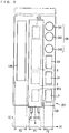
- Figs. 2 and 3 are plan views schematically showing spatial disposition of each part in the configuration of the power conversion device 201.
- the power conversion device 201 is disposed on a substrate 100, and Fig. 2 is a plan view as seen along a thickness direction of the substrate 100.
- the substrate 100 extends along a first direction Q1 and a second direction Q2 (here, a direction orthogonal to the first direction Q1) that are different from each other.
- a set 41d includes the switch Sl and the diode D40
- a set 42d includes the switch Sc and the current blocking element D43 on the assumption that the current blocking element D43 is provided. That is, Fig. 2 shows a case where the converter 2, the sets 41d and 42d, and the inverter 5 are disposed in that order along the second direction Q2.
- the power conversion device 201 further includes a cooler 8, which is not described in Fig. 1 , in addition to the components described in Fig. 1 .
- the cooler 8 extends along the second direction Q2 at the first position P1 in the first direction Q1, and cools at least the inverter 5 and, further in the examples of Figs. 2 and 3 , the converter 2 and the sets 41d and 42d.
- the capacitor C4 includes three capacitors C41, C42, and C43.
- the capacitors C41, C42, and C43, the capacitor C3, and the reactors L3 and L4 are disposed along the second direction Q2 at a second position P2, which is different from the first position P1, in the first direction Q1.
- the reactor L4 and the capacitor C4 are disposed in that order along the second direction Q2.
- Fig. 2 shows a case where the reactors L3 and L4 and the capacitors C3 and C4 are disposed in that order along the second direction Q2.
- At least one of a set of the reactor L4 and the converter 2 and a set of the capacitor C4 and the inverter 5 is disposed side by side along the first direction Q1.
- the disposition described above facilitates simplification of the wiring pattern in the power conversion device with a power buffer.
- the set of the reactor L4 and the converter 2 is not disposed side by side along the first direction Q1, but is disposed side by side with the set 41d (including the switch Sl). It is obvious that the disposition described above facilitates simplification of the wiring pattern that configures the charging circuit 41.
- the set of the capacitor C4 and the inverter 5 is disposed side by side along the first direction Q1.
- the output side of the discharging circuit 42 including the capacitor C4 is connected to the input side of the inverter 5, it is obvious that the disposition described above facilitates simplification of the wiring pattern provided between the discharging circuit 42 and the inverter 5.
- Fig. 3 shows a case where the set of the reactor L4 and the converter 2 is disposed side by side along the first direction Q1.
- the input side of the charging circuit 41 including the reactor L4 is connected to the output side of the converter 2, even with the low pass filter 3 interposed therebetween when the low pass filter 3 is provided, it is obvious that the disposition described above facilitates simplification of the wiring pattern provided between the charging circuit 41 and the converter 2.
- the capacitor C4 may be disposed side by side with the set 42d (including the switch Sc) along the first direction Q1. It is obvious that the disposition described above facilitates simplification of the wiring pattern that configures the discharging circuit 42.
- the diode D40 included in the charging circuit 41 is included in the set 41d as described above.
- the switch Sc included in the discharging circuit 42 is included in the set 42d. Therefore, it can be said that the diode D40 is disposed between the converter 2 and the switch Sc along the second direction Q2 at the first position P1.
- the discharging circuit 42 desirably includes the current blocking element D43 as described above.
- the current blocking element D43 is included in the set 42d as described above.
- the switch Sl included in the charging circuit 41 is included in the set 41d. Therefore, it can be said that the current blocking element D43 is disposed between the switch Sl and the inverter 5 along the second direction Q2 at the first position P1.
- the capacitor C3 and the reactor L3 thereof are desirably disposed along the second direction Q2 at the second position P2 while sandwiching the reactor L4.
- Figs. 2 and 3 show a case where the reactors L3 and L4 and the capacitor C3 are disposed in that order along the second direction Q2. This disposition is given in consideration of the fact that an amount of heat radiation of the capacitor C4 and the reactor L4, which store energy, is larger than that of the capacitor C3 and the reactor L3.
- the capacitor C3 and the reactor L3 sandwich the reactor L4, the capacitor C4 and the reactor L4 each having a large amount of heat radiation are prevented from being adjacent to each other, thereby preventing deterioration of the capacitor C4 (or of the reactor L4 as well) due to heat generation.
- the capacitor C3 and the reactors L4 and L3 being disposed in that order along the second direction Q2
- the control unit 109 is disposed at a third position P0 opposite to the second position P2 with respect to the first position P1. That is, the control unit 109 is disposed on the opposite side of the capacitor C4 and the reactor L4, or further of the capacitor C3 and the reactor L3 across the cooler 8. In the examples of Figs. 2 and 3 , the control unit 109, the cooler 8, the capacitor C4, and the reactor L4 are disposed in that order along the first direction Q1.
- the control unit 109 is disposed at the third position P0, the capacitor C4 and the reactor L4, or further the capacitor C3 and the reactor L3 are disposed at the second position P2, and the cooler 8 is disposed at the first position P1.
- the power conversion device 201 has the cooler 8 between the reactor L4 of the charging circuit 41 and the capacitor C4 of the discharging circuit 42, and the control unit 109. Therefore, the cooler 8 can reduce an influence of the heat radiation from the reactor L4 and the capacitor C4 on the control unit 109.
- the inverter 5 is cooled by the cooler 8, an influence of the heat radiation from the inverter 5 on the control unit 109 can also be reduced.
- the cooler 8 has a cooling jacket 80 and inflow and outflow pipes 81 and 82.
- the inflow and outflow pipes 81 and 82 guide inflow and outflow of the refrigerant to and from the cooling jacket 80.
- Fig. 4 is a schematic diagram showing a configuration of a refrigeration apparatus 300 including the power conversion device 201 and the load 6.
- the load 6 included in the refrigeration apparatus 300 is a compressor that includes a motor 61 and a compression element 62.
- the compression element 62 is driven by the motor 61 to compress a refrigerant M.
- Refrigerant paths B1 and B2 are connected to the compression element 62, and refrigerant paths B4 and B3 are connected to the inflow and outflow pipes 81 and 82, respectively.
- the refrigeration apparatus 300 configures a heat pump unit.
- the refrigerant M flows into the compression element 62 through the refrigerant path B1, and flows out of the compression element 62 through the refrigerant path B2.
- the refrigerant M flows into the cooling jacket 80 through the refrigerant path B4 and the inflow and outflow pipe 81, and flows out of the cooling jacket 80 through the inflow and outflow pipe 82 and the refrigerant path B3.
- heat exchangers such as an evaporator and a condenser, and an expander may be provided between the refrigerant paths B1 and B2 and the refrigerant paths B3 and B4.
- Fig. 4 shows a case where the refrigerant path B2, a condenser, an expander, and the refrigerant path B4 are connected in that order and the refrigerant M flows in that order, while the refrigerant path B3, an evaporator, and the refrigerant path B1 are connected in that order and the refrigerant M flows in that order.
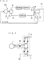
- Fig. 5 is a circuit diagram partially showing an electrical configuration of a power conversion device 202 according to a modification of the embodiment.
- the power conversion device 202 has a configuration in which a common mode choke CMC is added to the power conversion device 201.
- the common mode choke CMC is interposed between an AC power source 1 and a converter 2 (see, for example, Patent Document 4). That is, the configuration of the power conversion device 202 on a side electrically closer to an inverter 5 from the converter 2 is the same as that of the power conversion device 201. Therefore, in Fig. 5 , the diagram of the configuration on the side closer to the inverter 5 from the converter 2 is omitted.
- Fig. 6 is a plan view schematically showing spatial disposition of each part in the configuration of the power conversion device 202. Except for the disposition of the common mode choke CMC, the spatial disposition of the power conversion device 202 is the same as the spatial disposition of the power conversion device 201.
- the common mode choke CMC is disposed at a third position P0.
- the common mode choke CMC and a control unit 109 are disposed in that order along a second direction Q2.
- the common mode choke CMC, a cooler 8, and a reactor L3 are disposed in that order along a first direction Q1.
- the common mode choke CMC has a lower amount of heat radiation than the inverter 5, sets 41d and 42d, a capacitor C3, and a reactor L4. Therefore, even if the common mode choke CMC and the control unit 109 are disposed at the third position P0, which is the same side with respect to the cooler 8, the control unit 109 is not heavily affected by the heat generation from the common mode choke CMC.
- the common mode choke CMC is interposed between the AC power source 1 and the converter 2. Therefore, it is obvious that the disposition along the first direction Q1 side by side with the converter 2 facilitates simplification of the wiring pattern.
- the refrigeration apparatus 300 including the power conversion device 202 can be configured.
Landscapes
- Engineering & Computer Science (AREA)
- Power Engineering (AREA)
- Mechanical Engineering (AREA)
- General Engineering & Computer Science (AREA)
- Physics & Mathematics (AREA)
- Thermal Sciences (AREA)
- Chemical & Material Sciences (AREA)
- Combustion & Propulsion (AREA)
- Inverter Devices (AREA)
- Rectifiers (AREA)
- Dc-Dc Converters (AREA)
Abstract
Description
- The present invention relates to a power conversion device, and particularly to a direct-type power conversion device with a power buffer circuit.
- As a direct-type power conversion device, there has been known a configuration including a converter for performing AC-DC conversion, an inverter for performing DC-AC conversion, a pair of DC power source lines that connects the converter and the inverter, and a power buffer circuit for transferring power between the power buffer circuit and the pair of DC power source lines. The power buffer circuit includes a charging circuit and a discharging circuit.
- The discharging circuit includes a capacitor and a switching element. The switching element controls whether to allow discharge from the capacitor to the pair of DC power source lines. The charging circuit includes a reactor and a switching element. The switching element controls whether to store energy in the reactor or charge the capacitor of the discharging circuit with the stored energy. Hereinafter, a direct-type power conversion device having the configuration described above is temporarily referred to as a "power conversion device with a power buffer".
- There has also been known a configuration in which, in the power conversion device with a power buffer, a low pass filter is provided between the converter and the pair of DC power source lines. The configuration described above is introduced, for example, in
Patent Documents 1 and 2. Compared with a case where the low pass filter is provided on a front stage (AC power source side) of the converter, the configuration in which the low pass filter is provided between the converter and the pair of DC power source lines has an advantage of reducing a rated voltage of the capacitor that forms the low pass filter (see, for example, Patent Document 1). - In addition, there has been known an interleaved power source circuit including a power factor improvement circuit including a reactor, a diode, and a switching element, and a smoothing capacitor. There has also been known a configuration in which a reactor is disposed on an opposite side of a smoothing capacitor across a diode and a switching element that are to be cooled by a refrigerant jacket. The configuration described above is introduced, for example, in Patent Document 3.
- Note that
Patent Document 4 is listed as a prior art document that discloses a common mode choke for subsequent description. -
- Patent Document 1:
JP 2014-096976 A - Patent Document 2:
JP 2015-084637 A - Patent Document 3:
JP 2015-121364 A - Patent Document 4:
JP 2016-073025 A - It is true that the technique introduced in Patent Document 3 prevents the wiring pattern from becoming complicated in the printed wiring board on which the power factor improvement circuit and the smoothing capacitor are mounted. Moreover, through separate disposition of a low-voltage component group from a high-voltage component group, a low-voltage component is less likely to be adversely affected by a high-voltage component.
- However, the reactor included in the power factor improvement circuit and the smoothing capacitor are separated from each other by the switching element included in the power factor improvement circuit. Therefore, if the separation described above is applied to the power conversion device with a power buffer, and the switching element included in the discharging circuit and the switching element included in the charging circuit separate the capacitor included in the discharging circuit from the reactor included in the charging circuit, the wiring pattern may be rather complicated.
- Accordingly, an object of the present invention is to simplify a wiring pattern in a power conversion device with a power buffer.
- A power conversion device according to the present invention includes a converter (2) connected to an AC power source (1) to perform AC-DC conversion, a pair of DC power source lines (LH, LL) connected to an output side of the converter, a charging circuit (41) that includes a first reactor (L4) and a first switch (Sl) mutually connected in series between the pair of DC power source lines, receives power from the pair of DC power source lines via the first switch to store energy in the first reactor, and charges a first capacitor (C4) with the energy, a discharging circuit (42) that includes the first capacitor and a second switch (Sc) mutually connected in series between the pair of DC power source lines and applies power to the pair of DC power source lines through a discharge of the first capacitor via the second switch, and an inverter (5) that outputs an AC current (Iu, Iv, Iw) to a load (6) through DC-AC conversion of a first voltage (Vdc) between the pair of DC power source lines.
- Then, at a first position (P1) in a first direction (Q1), the converter, the first switch, the second switch, and the inverter are disposed in that order along a second direction (Q2) that is different from the first direction. Moreover, at a second position (P2) that is different from the first position in the first direction, the first reactor and the first capacitor are disposed in that order along the second direction. Furthermore, at least one of a set of the first reactor and the converter, and a set of the first capacitor and the inverter is disposed side by side along the first direction.
- A wiring pattern can be easily simplified in a power conversion device with a power buffer.
- The objects, features, aspects, and advantages of the present invention will be more apparent from the following detailed description and the accompanying drawings.
-
- [
Fig. 1 ] A circuit diagram showing a power conversion device according to the embodiment. - [
Fig. 2 ] A plan view showing the power conversion device according to the embodiment. - [
Fig. 3 ] A plan view showing the power conversion device according to the embodiment. - [
Fig. 4 ] A schematic diagram showing a refrigeration apparatus including the power conversion device according to the embodiment. - [
Fig. 5 ] A circuit diagram partially showing a power conversion device according to a modification of the embodiment. - [
Fig. 6 ] A plan view showing the power conversion device according to the modification of the embodiment. -
Fig. 1 is a circuit diagram showing an electrical configuration and transfer of signals of apower conversion device 201 according to the embodiment. Note that, since a detail of each component of the configuration described above is disclosed inPatent Documents 1 and 2, for example, detailed description is omitted. - In the circuit diagram, the
power conversion device 201 includes aconverter 2, a pair of DC power source lines LH and LL, acharging circuit 41, adischarging circuit 42, aninverter 5, and acontrol unit 109. It can be said that thepower conversion device 201 is the power conversion device with a power buffer described above. - The
converter 2 is connected to an AC power source 1 to perform AC-DC conversion. The pair of DC power source lines LH and LL is connected to an output side of theconverter 2. - In
Fig. 1 , a diode bridge that performs full-wave rectification is shown as theconverter 2. Specifically, theconverter 2 includes diodes D21, D22, D23, and D24. The AC power source 1 outputs single-phase AC voltage Vin, and the diodes D21 to D24 subject the single-phase AC voltage Vin to single-phase full-wave rectification to convert the single-phase AC voltage Vin into a rectified voltage, and then output the rectified voltage between the pair of DC power source lines LH and LL. - An input side of the
converter 2, that is, where the single-phase AC voltage Vin is input, is a pair of a connection point between an anode of the diode D21 and a cathode of the diode D22, and a connection point between an anode of the diode D23 and a cathode of the diode D24. - The output side of the
converter 2, that is, where the pair of DC power source lines LH and LL is connected, is a pair of a connection point between a cathode of the diode D21 and a cathode of the diode D23, and a connection point between an anode of the diode D22 and an anode of the diode D24. Specifically, the DC power source line LH is connected to the former connection point, and the DC power source line LL is connected to the latter connection point. Therefore, a potential higher than that of the DC power source line LL is applied to the DC power source line LH. - The
charging circuit 41 includes a reactor L4 and a switch Sl. The reactor L4 and the switch Sl are mutually connected in series between the pair of DC power source lines LH and LL. Thecharging circuit 41 receives power from the pair of DC power source lines LH and LL via the switch Sl, and stores energy in the reactor L4. Then, thecharging circuit 41 charges a capacitor C4 with the energy stored in the reactor L4. - The switch Sl is realized by, for example, a transistor (here, an insulated gate bipolar transistor (IGBT)).
- A diode D41 is connected reversely in parallel to the transistor that configures the switch Sl. Here, "connected reversely in parallel" refers to a parallel connection in which forward directions are opposite to each other. Specifically, a forward direction of the transistor that realizes the switch Sl is a direction from the DC power source line LH to the DC power source line LL, and a forward direction of the diode D41 is a direction from the DC power source line LL to the DC power source line LH.
- Since the DC power source line LH has a higher potential than the DC power source line LL, basically no current flows in the diode D41. Conduction or non-conduction of the switch Sl therefore depends almost exclusively on conduction or non-conduction of the transistor which realizes the switch Sl. Therefore, the transistor and the diode D41 may be collectively regarded as the switch Sl.
- The charging
circuit 41 further includes a diode D40. The diode D40 includes a cathode and an anode, and a charging current flows in the diode D40 to charge the capacitor C4. The cathode of the diode D40 is connected to the capacitor C4. - The reactor L4 is connected between the DC power source line LH and the anode of the diode D40. The switch Sl is connected between the DC power source line LL and the anode of the diode D40. The configuration described above is known as a so-called boost chopper.
- The discharging
circuit 42 includes the capacitor C4 and a switch Sc. The capacitor C4 and the switch Sc are mutually connected in series between the pair of DC power source lines LH and LL. Discharge of the capacitor C4 via the switch Sc causes the dischargingcircuit 42 to apply power to the pair of DC power source lines LH and LL. - The switch Sc is realized by, for example, a transistor (here, an IGBT). The diode D42 is connected reversely in parallel to the transistor that configures the switch Sc. A forward direction of the transistor that realizes the switch Sc is a direction from the DC power source line LL to the DC power source line LH, and a forward direction of the diode D42 is a direction from the DC power source line LH to the DC power source line LL.
- Since a voltage vc supported by the capacitor C4 is boosted by the charging
circuit 41, basically no current flows in the diode D42. Conduction or non-conduction of the switch Sc therefore depends exclusively on conduction or non-conduction of the transistor which realizes the switch Sc. Therefore, the transistor and the diode D42 may be collectively regarded as the switch Sc. - The charging
circuit 41 and the dischargingcircuit 42 configure apower buffer circuit 4 for transferring power between the pair of DC power source lines LH and LL. - The
inverter 5 inputs a voltage Vdc that is output from thepower buffer circuit 4 to the pair of DC power source lines LH and LL, performs DC-AC conversion on the voltage Vdc, and outputs an AC current to a load 6. For example, the load 6 is a three-phase inductive load, and theinverter 5 outputs AC currents Iu, Iv, and Iw. - The
inverter 5 includes output terminals Pu, Pv, and Pw, and outputs the AC currents Iu, Iv, and Iw therefrom. Theinverter 5 includes six switching elements Sup, Svp, Swp, Sun, Svn, and Swn. For example, IGBTs are adopted as the switching elements Sup, Svp, Swp, Sun, Svn, and Swn. - The switching elements Sup, Svp, and Swp are respectively connected between the output terminals Pu, Pv, and Pw and the DC power source line LH, and the switching elements Sun, Svn, and Swn are respectively connected between the output terminals Pu, Pv, and Pw and the DC power source line LL. The
inverter 5 configures a so-called voltage source inverter and includes six diodes. - All of the diodes described above have cathodes directed to the DC power source line LH side and anodes directed to the DC power source line LL side, and are connected reversely in parallel to the switching elements Sup, Svp, Swp, Sun, Svn, and Swn, respectively.
- The
control unit 109 includes aspeed detection unit 9 and a controlsignal generation unit 10. For example, the load 6 is a compressor that compresses a refrigerant, thespeed detection unit 9 detects the AC currents Iu, Iv, and Iw, and gives a rotational angular velocity ωm of the compressor obtained therefrom, and a q axis current Iq and a d axis current Id to the controlsignal generation unit 10. - The control
signal generation unit 10 further inputs amplitude Vm of the single-phase AC voltage Vin, amplitude Im and an electrical angular velocity ω of a current that flows into theconverter 2, and a command value ωm* of the rotational angular velocity ωm, and outputs switch control signals S41 and S42 for controlling the switches Sl and Sc, respectively, and an inverter control signal S5 for controlling theinverter 5. -
Fig. 1 shows a configuration in which thepower conversion device 201 also includes, although not necessary, a low pass filter 3. The low pass filter 3 is interposed between the output side of theconverter 2 and the pair of DC power source lines LH and LL. The low pass filter 3 includes a capacitor C3 and a reactor L3. The low pass filter 3 transmits, to the pair of DC power source lines LH and LL, a voltage v3 obtained through filtration of the output voltage of theconverter 2. However, rather than having a smoothing function, the low pass filter 3 has a function of preventing noise from theinverter 5 from being transmitted to a side of the AC power source 1. - The voltage v3 is supported by the capacitor C3. It can be said that the charging
circuit 41 boosts the voltage v3 to apply a voltage vc to the capacitor C4. - In this manner, in a case where the low pass filter 3 is provided, the discharging
circuit 42 further includes a current blocking element D43 in order to prevent discharge from the capacitor C4 to the capacitor C3 through conduction of the switch Sc. Specifically, the current blocking element D43 is provided on the DC power source line LH or the DC power source line LL between the capacitors C3 and C4. The current blocking element D43 is realized by, for example, a diode. In the example ofFig. 1 , the diode is provided on the DC power source line LH, and the forward direction thereof is a direction from theconverter 2 to theinverter 5. -
Figs. 2 and3 are plan views schematically showing spatial disposition of each part in the configuration of thepower conversion device 201. Thepower conversion device 201 is disposed on asubstrate 100, andFig. 2 is a plan view as seen along a thickness direction of thesubstrate 100. Thesubstrate 100 extends along a first direction Q1 and a second direction Q2 (here, a direction orthogonal to the first direction Q1) that are different from each other. - In
Figs.2 and3 , for simplicity, description of wiring that connects each element included in thepower conversion device 201 is omitted. For example, inFigs. 2 and3 , the pair of DC power source lines LH and LL is omitted. - At a first position P1 in the first direction Q1, the
converter 2, the switch Sl, the switch Sc, and theinverter 5 are disposed in that order along the second direction Q2. However, inFigs. 2 and3 , aset 41d includes the switch Sl and the diode D40, and aset 42d includes the switch Sc and the current blocking element D43 on the assumption that the current blocking element D43 is provided. That is,Fig. 2 shows a case where theconverter 2, thesets inverter 5 are disposed in that order along the second direction Q2. - In the configuration, the
power conversion device 201 further includes acooler 8, which is not described inFig. 1 , in addition to the components described inFig. 1 . Thecooler 8 extends along the second direction Q2 at the first position P1 in the first direction Q1, and cools at least theinverter 5 and, further in the examples ofFigs. 2 and3 , theconverter 2 and thesets - The capacitor C4 includes three capacitors C41, C42, and C43. The capacitors C41, C42, and C43, the capacitor C3, and the reactors L3 and L4 are disposed along the second direction Q2 at a second position P2, which is different from the first position P1, in the first direction Q1. Specifically, the reactor L4 and the capacitor C4 are disposed in that order along the second direction Q2. Although specific disposition of the capacitor C3 and the reactor L3 will be described later,
Fig. 2 shows a case where the reactors L3 and L4 and the capacitors C3 and C4 are disposed in that order along the second direction Q2. - In the
power conversion device 201, at least one of a set of the reactor L4 and theconverter 2 and a set of the capacitor C4 and theinverter 5 is disposed side by side along the first direction Q1. - The disposition described above facilitates simplification of the wiring pattern in the power conversion device with a power buffer. Specifically, in the example shown in
Fig. 2 , the set of the reactor L4 and theconverter 2 is not disposed side by side along the first direction Q1, but is disposed side by side with theset 41d (including the switch Sl). It is obvious that the disposition described above facilitates simplification of the wiring pattern that configures the chargingcircuit 41. - On the other hand, the set of the capacitor C4 and the
inverter 5 is disposed side by side along the first direction Q1. With reference toFig. 1 , in view of the fact that the output side of the dischargingcircuit 42 including the capacitor C4 is connected to the input side of theinverter 5, it is obvious that the disposition described above facilitates simplification of the wiring pattern provided between the dischargingcircuit 42 and theinverter 5. -
Fig. 3 shows a case where the set of the reactor L4 and theconverter 2 is disposed side by side along the first direction Q1. In this case, in view of the fact that the input side of the chargingcircuit 41 including the reactor L4 is connected to the output side of theconverter 2, even with the low pass filter 3 interposed therebetween when the low pass filter 3 is provided, it is obvious that the disposition described above facilitates simplification of the wiring pattern provided between the chargingcircuit 41 and theconverter 2. - As shown in
Fig. 3 , the capacitor C4 may be disposed side by side with theset 42d (including the switch Sc) along the first direction Q1. It is obvious that the disposition described above facilitates simplification of the wiring pattern that configures the dischargingcircuit 42. - Note that the diode D40 included in the charging
circuit 41 is included in theset 41d as described above. Moreover, the switch Sc included in the dischargingcircuit 42 is included in theset 42d. Therefore, it can be said that the diode D40 is disposed between theconverter 2 and the switch Sc along the second direction Q2 at the first position P1. - In addition, when the low pass filter 3 is provided, the discharging
circuit 42 desirably includes the current blocking element D43 as described above. The current blocking element D43 is included in theset 42d as described above. Moreover, the switch Sl included in the chargingcircuit 41 is included in theset 41d. Therefore, it can be said that the current blocking element D43 is disposed between the switch Sl and theinverter 5 along the second direction Q2 at the first position P1. - As described thus far, it is obvious that combining the diode D40 with the switch Sl in the
set 41d and the current blocking element D43 with the switch Sc in theset 42d also facilitates simplification of the wiring pattern. - Further, when the low pass filter 3 is provided, the capacitor C3 and the reactor L3 thereof are desirably disposed along the second direction Q2 at the second position P2 while sandwiching the reactor L4.
Figs. 2 and3 show a case where the reactors L3 and L4 and the capacitor C3 are disposed in that order along the second direction Q2. This disposition is given in consideration of the fact that an amount of heat radiation of the capacitor C4 and the reactor L4, which store energy, is larger than that of the capacitor C3 and the reactor L3. Since the capacitor C3 and the reactor L3 sandwich the reactor L4, the capacitor C4 and the reactor L4 each having a large amount of heat radiation are prevented from being adjacent to each other, thereby preventing deterioration of the capacitor C4 (or of the reactor L4 as well) due to heat generation. - However, rather than the capacitor C3 and the reactors L4 and L3 being disposed in that order along the second direction Q2, it is desirable, as shown in
Figs. 2 and3 , that the reactors L3 and L4 and the capacitor C3 be disposed in that order. That is, the capacitor C3 is desirably disposed between the reactor L4 and the capacitor C4 along the second direction Q2 at the second position P2. This is because the reactor L3 is connected on a side closer to theconverter 2 than the capacitor C3 is (see alsoFig. 1 ), the wiring pattern can be easily simplified. - The
control unit 109 is disposed at a third position P0 opposite to the second position P2 with respect to the first position P1. That is, thecontrol unit 109 is disposed on the opposite side of the capacitor C4 and the reactor L4, or further of the capacitor C3 and the reactor L3 across thecooler 8. In the examples ofFigs. 2 and3 , thecontrol unit 109, thecooler 8, the capacitor C4, and the reactor L4 are disposed in that order along the first direction Q1. - The
control unit 109 is disposed at the third position P0, the capacitor C4 and the reactor L4, or further the capacitor C3 and the reactor L3 are disposed at the second position P2, and thecooler 8 is disposed at the first position P1. By adopting such disposition, thepower conversion device 201 has thecooler 8 between the reactor L4 of the chargingcircuit 41 and the capacitor C4 of the dischargingcircuit 42, and thecontrol unit 109. Therefore, thecooler 8 can reduce an influence of the heat radiation from the reactor L4 and the capacitor C4 on thecontrol unit 109. In addition, since theinverter 5 is cooled by thecooler 8, an influence of the heat radiation from theinverter 5 on thecontrol unit 109 can also be reduced. - The
cooler 8 has a coolingjacket 80 and inflow andoutflow pipes outflow pipes jacket 80. -
Fig. 4 is a schematic diagram showing a configuration of arefrigeration apparatus 300 including thepower conversion device 201 and the load 6. InFig. 4 , the internal configuration of thepower conversion device 201 is omitted except for thecooler 8. The load 6 included in therefrigeration apparatus 300 is a compressor that includes amotor 61 and acompression element 62. Thecompression element 62 is driven by themotor 61 to compress a refrigerant M. Refrigerant paths B1 and B2 are connected to thecompression element 62, and refrigerant paths B4 and B3 are connected to the inflow andoutflow pipes refrigeration apparatus 300 configures a heat pump unit. - The refrigerant M flows into the
compression element 62 through the refrigerant path B1, and flows out of thecompression element 62 through the refrigerant path B2. The refrigerant M flows into the coolingjacket 80 through the refrigerant path B4 and the inflow andoutflow pipe 81, and flows out of the coolingjacket 80 through the inflow andoutflow pipe 82 and the refrigerant path B3. - For example, heat exchangers such as an evaporator and a condenser, and an expander may be provided between the refrigerant paths B1 and B2 and the refrigerant paths B3 and B4.
Fig. 4 shows a case where the refrigerant path B2, a condenser, an expander, and the refrigerant path B4 are connected in that order and the refrigerant M flows in that order, while the refrigerant path B3, an evaporator, and the refrigerant path B1 are connected in that order and the refrigerant M flows in that order. -
Fig. 5 is a circuit diagram partially showing an electrical configuration of apower conversion device 202 according to a modification of the embodiment. Thepower conversion device 202 has a configuration in which a common mode choke CMC is added to thepower conversion device 201. The common mode choke CMC is interposed between an AC power source 1 and a converter 2 (see, for example, Patent Document 4). That is, the configuration of thepower conversion device 202 on a side electrically closer to aninverter 5 from theconverter 2 is the same as that of thepower conversion device 201. Therefore, inFig. 5 , the diagram of the configuration on the side closer to theinverter 5 from theconverter 2 is omitted. -
Fig. 6 is a plan view schematically showing spatial disposition of each part in the configuration of thepower conversion device 202. Except for the disposition of the common mode choke CMC, the spatial disposition of thepower conversion device 202 is the same as the spatial disposition of thepower conversion device 201. - The common mode choke CMC is disposed at a third position P0. In the example of
Fig. 6 , the common mode choke CMC and acontrol unit 109 are disposed in that order along a second direction Q2. Moreover, in the example ofFig. 6 , the common mode choke CMC, acooler 8, and a reactor L3 are disposed in that order along a first direction Q1. - The common mode choke CMC has a lower amount of heat radiation than the
inverter 5, sets 41d and 42d, a capacitor C3, and a reactor L4. Therefore, even if the common mode choke CMC and thecontrol unit 109 are disposed at the third position P0, which is the same side with respect to thecooler 8, thecontrol unit 109 is not heavily affected by the heat generation from the common mode choke CMC. - In addition, the common mode choke CMC is interposed between the AC power source 1 and the
converter 2. Therefore, it is obvious that the disposition along the first direction Q1 side by side with theconverter 2 facilitates simplification of the wiring pattern. - Of course, in the same manner as the
power conversion device 201 shown inFig. 4 , therefrigeration apparatus 300 including thepower conversion device 202 can be configured. - Although the present invention has been described in detail, the above description is illustrative in all aspects, and the present invention is not limited to the above description. It is understood that countless variations not illustrated are conceivable without departing from the scope of the present invention.
Claims (8)
- A power conversion device (201, 202) comprising:a converter (2) connected to an AC power source (1) to perform AC-DC conversion;a pair of DC power source lines (LH, LL) connected to an output side of the converter;a charging circuit (41) that includes a first reactor (L4) and a first switch (S1) mutually connected in series between the pair of DC power source lines, receives power from the pair of DC power source lines via the first switch to store energy in the first reactor, and charges a first capacitor (C4) with the energy;a discharging circuit (42) that includes the first capacitor and a second switch (Sc) mutually connected in series between the pair of DC power source lines, and applies power to the pair of DC power source lines through a discharge of the first capacitor via the second switch; andan inverter (5) that outputs an AC current (Iu, Iv, Iw) to a load (6) through DC-AC conversion of a first voltage (Vdc) between the pair of DC power source lines,wherein at a first position (P1) in a first direction (Q1), the converter, the first switch, the second switch, and the inverter are disposed in that order along a second direction (Q2) that is different from the first direction,at a second position (P2) that is different from the first position in the first direction, the first reactor and the first capacitor are disposed in that order along the second direction, andat least one of a set of the first reactor and the converter, and a set of the first capacitor and the inverter is disposed side by side along the first direction.
- The power conversion device (201, 202) according to claim 1,
wherein the first reactor is disposed side by side with the converter or the first switch along the first direction, and
the first capacitor is disposed side by side with the inverter or the second switch along the first direction. - The power conversion device according to claim 1 or 2,
wherein the charging circuit (41) further includes a diode (D40) through which a charging current for charging the first capacitor (C4) flows, and
the diode is disposed between the converter (2) and the second switch (Sc) along the second direction (Q2) at the first position (P1). - The power conversion device according to any one of claims 1 to 3, further comprising a low pass filter (3) that is interposed between an output side of the converter (2) and the pair of DC power source lines (LH, LL), includes a second capacitor (C3) and a second reactor (L3), and transmits, to the pair of DC power source lines, a second voltage (v3) obtained through filtration of an output voltage of the converter,
wherein the discharging circuit (42) further includes a current blocking element (D43) that blocks a current from the first capacitor to the low pass filter (3),
the current blocking element is disposed between the first switch (Sl) and the inverter (5) along the second direction (Q2) at the first position (P1), and
the second capacitor (C3) and the second reactor (L3) are disposed while sandwiching the first reactor along the second direction (Q2) at the second position (P2). - The power conversion device according to claim 4,
wherein the second capacitor (C3) is disposed between the first reactor (L4) and the first capacitor (C4) along the second direction (Q2) at the second position (P2). - The power conversion device (202) according to any one of claims 1 to 5, further comprising a common mode choke (CMC) that is interposed between the AC power source (1) and the converter (2), disposed at a third position (P0) opposite to the second position with respect to the first position (P1), and disposed side by side with the converter (2) along the first direction (Q1).
- The power conversion device (201, 202) according to any one of claims 1 to 6, further comprising a cooler (8) that is disposed at the first position (P1) and cools at least the inverter (5).
- A refrigeration apparatus (300) comprising:the power conversion device (201, 202) according to claim 7; andthe load (6),wherein the load is a compressor that compresses a refrigerant (M) that flows into the cooler.
Applications Claiming Priority (2)
| Application Number | Priority Date | Filing Date | Title |
|---|---|---|---|
| JP2017106358A JP6394741B1 (en) | 2017-05-30 | 2017-05-30 | Power converter, refrigeration equipment |
| PCT/JP2018/020151 WO2018221407A1 (en) | 2017-05-30 | 2018-05-25 | Power conversion device and refrigeration device |
Publications (3)
| Publication Number | Publication Date |
|---|---|
| EP3633842A1 true EP3633842A1 (en) | 2020-04-08 |
| EP3633842A4 EP3633842A4 (en) | 2021-01-13 |
| EP3633842B1 EP3633842B1 (en) | 2023-05-03 |
Family
ID=63668483
Family Applications (1)
| Application Number | Title | Priority Date | Filing Date |
|---|---|---|---|
| EP18810261.0A Active EP3633842B1 (en) | 2017-05-30 | 2018-05-25 | Power conversion device and refrigeration device |
Country Status (6)
| Country | Link |
|---|---|
| US (1) | US10739019B2 (en) |
| EP (1) | EP3633842B1 (en) |
| JP (1) | JP6394741B1 (en) |
| CN (1) | CN110679075B (en) |
| AU (1) | AU2018276521B2 (en) |
| WO (1) | WO2018221407A1 (en) |
Families Citing this family (2)
| Publication number | Priority date | Publication date | Assignee | Title |
|---|---|---|---|---|
| CN211908640U (en) * | 2020-05-19 | 2020-11-10 | 阳光电源股份有限公司 | Power conversion device |
| GB2604188A (en) * | 2021-02-22 | 2022-08-31 | Edwards Tech Vacuum Engineering Qingdao Co Ltd | Control of liquid ring pump |
Family Cites Families (30)
| Publication number | Priority date | Publication date | Assignee | Title |
|---|---|---|---|---|
| JP2001054286A (en) * | 1999-08-06 | 2001-02-23 | Mitsubishi Electric Corp | Electronic control board |
| JP2002291260A (en) * | 2001-03-26 | 2002-10-04 | Mitsubishi Electric Corp | Motor control device and compressor using the same |
| US7164242B2 (en) * | 2004-02-27 | 2007-01-16 | York International Corp. | Variable speed drive for multiple loads |
| US7176648B2 (en) * | 2004-05-18 | 2007-02-13 | Husky Injection Molding Systems Ltd. | Energy management apparatus and method for injection molding systems |
| FR2881018B1 (en) * | 2005-01-19 | 2007-04-06 | Intelligent Electronic Systems | METHOD FOR COOLING A STATIC POWER CONVERSION DEVICE AND CORRESPONDING DEVICE |
| US9192079B2 (en) * | 2008-09-26 | 2015-11-17 | Rockwell Automation Technologies, Inc. | Power electronic module cooling system and method |
| CN201336630Y (en) | 2009-01-04 | 2009-10-28 | 青岛海信电器股份有限公司 | Power supply circuit and electrical appliance with same |
| CN102971946B (en) * | 2010-07-06 | 2016-03-16 | 三菱电机株式会社 | inverter |
| JP5472364B2 (en) * | 2012-04-20 | 2014-04-16 | ダイキン工業株式会社 | Refrigeration equipment |
| JP5397497B2 (en) * | 2012-04-20 | 2014-01-22 | ダイキン工業株式会社 | Refrigeration equipment |
| JP5408285B2 (en) * | 2012-04-27 | 2014-02-05 | ダイキン工業株式会社 | Refrigerator, electrical component unit and refrigeration system |
| CN104641543B (en) * | 2012-09-21 | 2016-04-27 | 大金工业株式会社 | Control method of direct type power conversion device |
| EP2903148B1 (en) * | 2012-09-27 | 2021-02-17 | Daikin Industries, Ltd. | Direct ac power conversion device |
| WO2014057883A1 (en) * | 2012-10-10 | 2014-04-17 | ダイキン工業株式会社 | Direct power conversion device and method for controlling direct power conversion device |
| JP6065262B2 (en) * | 2012-10-12 | 2017-01-25 | 富士電機株式会社 | Power supply |
| JP5804167B2 (en) | 2013-09-19 | 2015-11-04 | ダイキン工業株式会社 | Power converter |
| JP5794273B2 (en) * | 2013-10-07 | 2015-10-14 | ダイキン工業株式会社 | Control method for direct power converter |
| JP5804019B2 (en) * | 2013-10-16 | 2015-11-04 | ダイキン工業株式会社 | Power converter |
| JP5842905B2 (en) * | 2013-12-24 | 2016-01-13 | ダイキン工業株式会社 | Refrigeration equipment |
| US9353968B2 (en) * | 2014-03-27 | 2016-05-31 | Daikin Industries, Ltd. | Heat source unit of refrigerating apparatus |
| CN106471725B (en) * | 2014-07-18 | 2018-02-27 | 大金工业株式会社 | Direct Type AC Power Converter |
| JP5930108B2 (en) * | 2014-09-25 | 2016-06-08 | ダイキン工業株式会社 | Power converter |
| JP5850116B1 (en) * | 2014-09-26 | 2016-02-03 | ダイキン工業株式会社 | Power converter |
| JP2016109350A (en) * | 2014-12-05 | 2016-06-20 | ダイキン工業株式会社 | Refrigeration device |
| EP3273585B1 (en) * | 2015-03-16 | 2023-04-26 | Mitsubishi Electric Corporation | Power circuit device |
| JP6103031B1 (en) * | 2015-12-28 | 2017-03-29 | ダイキン工業株式会社 | Control device for power converter |
| JP6094665B1 (en) * | 2015-12-28 | 2017-03-15 | ダイキン工業株式会社 | Control device for power converter |
| JP6265297B1 (en) * | 2016-09-30 | 2018-01-24 | ダイキン工業株式会社 | Control device for direct power converter. |
| JP6702209B2 (en) * | 2017-01-26 | 2020-05-27 | 株式会社デンソー | Power converter |
| WO2019088678A1 (en) * | 2017-11-02 | 2019-05-09 | Samsung Electronics Co., Ltd. | Air conditioner and rectifier |
-
2017
- 2017-05-30 JP JP2017106358A patent/JP6394741B1/en active Active
-
2018
- 2018-05-25 EP EP18810261.0A patent/EP3633842B1/en active Active
- 2018-05-25 WO PCT/JP2018/020151 patent/WO2018221407A1/en not_active Ceased
- 2018-05-25 CN CN201880034374.1A patent/CN110679075B/en active Active
- 2018-05-25 AU AU2018276521A patent/AU2018276521B2/en active Active
- 2018-05-25 US US16/617,700 patent/US10739019B2/en active Active
Also Published As
| Publication number | Publication date |
|---|---|
| EP3633842A4 (en) | 2021-01-13 |
| US20200112248A1 (en) | 2020-04-09 |
| CN110679075B (en) | 2021-01-05 |
| AU2018276521A1 (en) | 2019-12-19 |
| JP6394741B1 (en) | 2018-09-26 |
| CN110679075A (en) | 2020-01-10 |
| WO2018221407A1 (en) | 2018-12-06 |
| JP2018207555A (en) | 2018-12-27 |
| EP3633842B1 (en) | 2023-05-03 |
| US10739019B2 (en) | 2020-08-11 |
| AU2018276521B2 (en) | 2020-01-16 |
Similar Documents
| Publication | Publication Date | Title |
|---|---|---|
| US10230298B2 (en) | Resistorless precharging | |
| US7830036B2 (en) | Power electronic module pre-charge system and method | |
| EP3048718B1 (en) | Power conversion device | |
| US9450502B2 (en) | Direct power conversion device and method for controlling direct power conversion device | |
| US20120069604A1 (en) | Compact power converter with high efficiency in operation | |
| US20160036323A1 (en) | Three port dc-dc converter | |
| US9035578B2 (en) | System for coupling at least one DC source to a controllable energy store and associated operating method | |
| US20130285456A1 (en) | Controllable energy store and method for operating a controllable energy store | |
| US9793710B2 (en) | Energy storing device with cooling elements, and method for cooling energy storing cells | |
| US9564797B2 (en) | Indirect matrix converter | |
| WO2013035383A1 (en) | Power conversion device | |
| WO2024032463A1 (en) | Dc/dc converter, method for controlling output voltage thereof, and energy storage system | |
| US20130257355A1 (en) | System for charging an energy store, and method for operating the charging system | |
| CN114337328A (en) | Electronic circuit and air conditioner | |
| EP3633842B1 (en) | Power conversion device and refrigeration device | |
| WO2017096355A1 (en) | Power converter circuitry for photovoltaic devices | |
| CN109450243B (en) | PFC circuit, motor control system and air conditioner | |
| US9425723B2 (en) | System comprising an electrically excited machine | |
| EP4216427B1 (en) | Motor control system and vehicle | |
| CN103296910A (en) | Direct voltage capture device for energy storage device and method for generating direct voltage by energy storage device | |
| JP6597714B2 (en) | Power converter, refrigeration equipment | |
| US20230275525A1 (en) | Electric circuit and air conditioner | |
| CN209233733U (en) | The frequency-variable controller and air conditioner of three phase mains | |
| EP4550647A1 (en) | Power converters and methods of controlling a power converter | |
| CN120613940B (en) | AC-DC converter with AC-DC common ground and bipolar DC voltage balance function |
Legal Events
| Date | Code | Title | Description |
|---|---|---|---|
| STAA | Information on the status of an ep patent application or granted ep patent |
Free format text: STATUS: THE INTERNATIONAL PUBLICATION HAS BEEN MADE |
|
| PUAI | Public reference made under article 153(3) epc to a published international application that has entered the european phase |
Free format text: ORIGINAL CODE: 0009012 |
|
| STAA | Information on the status of an ep patent application or granted ep patent |
Free format text: STATUS: REQUEST FOR EXAMINATION WAS MADE |
|
| 17P | Request for examination filed |
Effective date: 20191122 |
|
| AK | Designated contracting states |
Kind code of ref document: A1 Designated state(s): AL AT BE BG CH CY CZ DE DK EE ES FI FR GB GR HR HU IE IS IT LI LT LU LV MC MK MT NL NO PL PT RO RS SE SI SK SM TR |
|
| AX | Request for extension of the european patent |
Extension state: BA ME |
|
| DAV | Request for validation of the european patent (deleted) | ||
| DAX | Request for extension of the european patent (deleted) | ||
| A4 | Supplementary search report drawn up and despatched |
Effective date: 20201215 |
|
| RIC1 | Information provided on ipc code assigned before grant |
Ipc: H02M 7/00 20060101AFI20201209BHEP Ipc: H02M 5/458 20060101ALN20201209BHEP |
|
| STAA | Information on the status of an ep patent application or granted ep patent |
Free format text: STATUS: EXAMINATION IS IN PROGRESS |
|
| 17Q | First examination report despatched |
Effective date: 20210802 |
|
| RIC1 | Information provided on ipc code assigned before grant |
Ipc: H02M 5/458 20060101ALN20220719BHEP Ipc: H02M 7/00 20060101AFI20220719BHEP |
|
| GRAP | Despatch of communication of intention to grant a patent |
Free format text: ORIGINAL CODE: EPIDOSNIGR1 |
|
| STAA | Information on the status of an ep patent application or granted ep patent |
Free format text: STATUS: GRANT OF PATENT IS INTENDED |
|
| RIC1 | Information provided on ipc code assigned before grant |
Ipc: H02M 5/458 20060101ALN20220819BHEP Ipc: H02M 7/00 20060101AFI20220819BHEP |
|
| INTG | Intention to grant announced |
Effective date: 20220913 |
|
| GRAJ | Information related to disapproval of communication of intention to grant by the applicant or resumption of examination proceedings by the epo deleted |
Free format text: ORIGINAL CODE: EPIDOSDIGR1 |
|
| STAA | Information on the status of an ep patent application or granted ep patent |
Free format text: STATUS: EXAMINATION IS IN PROGRESS |
|
| REG | Reference to a national code |
Ref country code: DE Ref legal event code: R079 Ref document number: 602018049313 Country of ref document: DE Free format text: PREVIOUS MAIN CLASS: H02M0007480000 Ipc: H02M0007000000 |
|
| GRAP | Despatch of communication of intention to grant a patent |
Free format text: ORIGINAL CODE: EPIDOSNIGR1 |
|
| STAA | Information on the status of an ep patent application or granted ep patent |
Free format text: STATUS: GRANT OF PATENT IS INTENDED |
|
| INTC | Intention to grant announced (deleted) | ||
| RIC1 | Information provided on ipc code assigned before grant |
Ipc: H02M 5/458 20060101ALN20221110BHEP Ipc: H02M 7/00 20060101AFI20221110BHEP |
|
| INTG | Intention to grant announced |
Effective date: 20221130 |
|
| RAP3 | Party data changed (applicant data changed or rights of an application transferred) |
Owner name: DAIKIN INDUSTRIES, LTD. |
|
| GRAS | Grant fee paid |
Free format text: ORIGINAL CODE: EPIDOSNIGR3 |
|
| GRAA | (expected) grant |
Free format text: ORIGINAL CODE: 0009210 |
|
| STAA | Information on the status of an ep patent application or granted ep patent |
Free format text: STATUS: THE PATENT HAS BEEN GRANTED |
|
| AK | Designated contracting states |
Kind code of ref document: B1 Designated state(s): AL AT BE BG CH CY CZ DE DK EE ES FI FR GB GR HR HU IE IS IT LI LT LU LV MC MK MT NL NO PL PT RO RS SE SI SK SM TR |
|
| REG | Reference to a national code |
Ref country code: GB Ref legal event code: FG4D |
|
| REG | Reference to a national code |
Ref country code: DE Ref legal event code: R096 Ref document number: 602018049313 Country of ref document: DE |
|
| REG | Reference to a national code |
Ref country code: AT Ref legal event code: REF Ref document number: 1565531 Country of ref document: AT Kind code of ref document: T Effective date: 20230515 Ref country code: CH Ref legal event code: EP |
|
| REG | Reference to a national code |
Ref country code: IE Ref legal event code: FG4D |
|
| P01 | Opt-out of the competence of the unified patent court (upc) registered |
Effective date: 20230525 |
|
| REG | Reference to a national code |
Ref country code: LT Ref legal event code: MG9D |
|
| REG | Reference to a national code |
Ref country code: NL Ref legal event code: MP Effective date: 20230503 |
|
| REG | Reference to a national code |
Ref country code: AT Ref legal event code: MK05 Ref document number: 1565531 Country of ref document: AT Kind code of ref document: T Effective date: 20230503 |
|
| PG25 | Lapsed in a contracting state [announced via postgrant information from national office to epo] |
Ref country code: SE Free format text: LAPSE BECAUSE OF FAILURE TO SUBMIT A TRANSLATION OF THE DESCRIPTION OR TO PAY THE FEE WITHIN THE PRESCRIBED TIME-LIMIT Effective date: 20230503 Ref country code: PT Free format text: LAPSE BECAUSE OF FAILURE TO SUBMIT A TRANSLATION OF THE DESCRIPTION OR TO PAY THE FEE WITHIN THE PRESCRIBED TIME-LIMIT Effective date: 20230904 Ref country code: NO Free format text: LAPSE BECAUSE OF FAILURE TO SUBMIT A TRANSLATION OF THE DESCRIPTION OR TO PAY THE FEE WITHIN THE PRESCRIBED TIME-LIMIT Effective date: 20230803 Ref country code: NL Free format text: LAPSE BECAUSE OF FAILURE TO SUBMIT A TRANSLATION OF THE DESCRIPTION OR TO PAY THE FEE WITHIN THE PRESCRIBED TIME-LIMIT Effective date: 20230503 Ref country code: ES Free format text: LAPSE BECAUSE OF FAILURE TO SUBMIT A TRANSLATION OF THE DESCRIPTION OR TO PAY THE FEE WITHIN THE PRESCRIBED TIME-LIMIT Effective date: 20230503 Ref country code: AT Free format text: LAPSE BECAUSE OF FAILURE TO SUBMIT A TRANSLATION OF THE DESCRIPTION OR TO PAY THE FEE WITHIN THE PRESCRIBED TIME-LIMIT Effective date: 20230503 |
|
| PG25 | Lapsed in a contracting state [announced via postgrant information from national office to epo] |
Ref country code: RS Free format text: LAPSE BECAUSE OF FAILURE TO SUBMIT A TRANSLATION OF THE DESCRIPTION OR TO PAY THE FEE WITHIN THE PRESCRIBED TIME-LIMIT Effective date: 20230503 Ref country code: PL Free format text: LAPSE BECAUSE OF FAILURE TO SUBMIT A TRANSLATION OF THE DESCRIPTION OR TO PAY THE FEE WITHIN THE PRESCRIBED TIME-LIMIT Effective date: 20230503 Ref country code: LV Free format text: LAPSE BECAUSE OF FAILURE TO SUBMIT A TRANSLATION OF THE DESCRIPTION OR TO PAY THE FEE WITHIN THE PRESCRIBED TIME-LIMIT Effective date: 20230503 Ref country code: LT Free format text: LAPSE BECAUSE OF FAILURE TO SUBMIT A TRANSLATION OF THE DESCRIPTION OR TO PAY THE FEE WITHIN THE PRESCRIBED TIME-LIMIT Effective date: 20230503 Ref country code: IS Free format text: LAPSE BECAUSE OF FAILURE TO SUBMIT A TRANSLATION OF THE DESCRIPTION OR TO PAY THE FEE WITHIN THE PRESCRIBED TIME-LIMIT Effective date: 20230903 Ref country code: HR Free format text: LAPSE BECAUSE OF FAILURE TO SUBMIT A TRANSLATION OF THE DESCRIPTION OR TO PAY THE FEE WITHIN THE PRESCRIBED TIME-LIMIT Effective date: 20230503 Ref country code: GR Free format text: LAPSE BECAUSE OF FAILURE TO SUBMIT A TRANSLATION OF THE DESCRIPTION OR TO PAY THE FEE WITHIN THE PRESCRIBED TIME-LIMIT Effective date: 20230804 |
|
| PG25 | Lapsed in a contracting state [announced via postgrant information from national office to epo] |
Ref country code: FI Free format text: LAPSE BECAUSE OF FAILURE TO SUBMIT A TRANSLATION OF THE DESCRIPTION OR TO PAY THE FEE WITHIN THE PRESCRIBED TIME-LIMIT Effective date: 20230503 |
|
| REG | Reference to a national code |
Ref country code: CH Ref legal event code: PL |
|
| PG25 | Lapsed in a contracting state [announced via postgrant information from national office to epo] |
Ref country code: SK Free format text: LAPSE BECAUSE OF FAILURE TO SUBMIT A TRANSLATION OF THE DESCRIPTION OR TO PAY THE FEE WITHIN THE PRESCRIBED TIME-LIMIT Effective date: 20230503 |
|
| REG | Reference to a national code |
Ref country code: BE Ref legal event code: MM Effective date: 20230531 |
|
| PG25 | Lapsed in a contracting state [announced via postgrant information from national office to epo] |
Ref country code: SM Free format text: LAPSE BECAUSE OF FAILURE TO SUBMIT A TRANSLATION OF THE DESCRIPTION OR TO PAY THE FEE WITHIN THE PRESCRIBED TIME-LIMIT Effective date: 20230503 Ref country code: SK Free format text: LAPSE BECAUSE OF FAILURE TO SUBMIT A TRANSLATION OF THE DESCRIPTION OR TO PAY THE FEE WITHIN THE PRESCRIBED TIME-LIMIT Effective date: 20230503 Ref country code: RO Free format text: LAPSE BECAUSE OF FAILURE TO SUBMIT A TRANSLATION OF THE DESCRIPTION OR TO PAY THE FEE WITHIN THE PRESCRIBED TIME-LIMIT Effective date: 20230503 Ref country code: LU Free format text: LAPSE BECAUSE OF NON-PAYMENT OF DUE FEES Effective date: 20230525 Ref country code: LI Free format text: LAPSE BECAUSE OF NON-PAYMENT OF DUE FEES Effective date: 20230531 Ref country code: EE Free format text: LAPSE BECAUSE OF FAILURE TO SUBMIT A TRANSLATION OF THE DESCRIPTION OR TO PAY THE FEE WITHIN THE PRESCRIBED TIME-LIMIT Effective date: 20230503 Ref country code: DK Free format text: LAPSE BECAUSE OF FAILURE TO SUBMIT A TRANSLATION OF THE DESCRIPTION OR TO PAY THE FEE WITHIN THE PRESCRIBED TIME-LIMIT Effective date: 20230503 Ref country code: CZ Free format text: LAPSE BECAUSE OF FAILURE TO SUBMIT A TRANSLATION OF THE DESCRIPTION OR TO PAY THE FEE WITHIN THE PRESCRIBED TIME-LIMIT Effective date: 20230503 Ref country code: CH Free format text: LAPSE BECAUSE OF NON-PAYMENT OF DUE FEES Effective date: 20230531 |
|
| REG | Reference to a national code |
Ref country code: DE Ref legal event code: R097 Ref document number: 602018049313 Country of ref document: DE |
|
| PG25 | Lapsed in a contracting state [announced via postgrant information from national office to epo] |
Ref country code: MC Free format text: LAPSE BECAUSE OF FAILURE TO SUBMIT A TRANSLATION OF THE DESCRIPTION OR TO PAY THE FEE WITHIN THE PRESCRIBED TIME-LIMIT Effective date: 20230503 |
|
| REG | Reference to a national code |
Ref country code: IE Ref legal event code: MM4A |
|
| PG25 | Lapsed in a contracting state [announced via postgrant information from national office to epo] |
Ref country code: MC Free format text: LAPSE BECAUSE OF FAILURE TO SUBMIT A TRANSLATION OF THE DESCRIPTION OR TO PAY THE FEE WITHIN THE PRESCRIBED TIME-LIMIT Effective date: 20230503 |
|
| PLBE | No opposition filed within time limit |
Free format text: ORIGINAL CODE: 0009261 |
|
| STAA | Information on the status of an ep patent application or granted ep patent |
Free format text: STATUS: NO OPPOSITION FILED WITHIN TIME LIMIT |
|
| 26N | No opposition filed |
Effective date: 20240206 |
|
| PG25 | Lapsed in a contracting state [announced via postgrant information from national office to epo] |
Ref country code: IE Free format text: LAPSE BECAUSE OF NON-PAYMENT OF DUE FEES Effective date: 20230525 |
|
| PG25 | Lapsed in a contracting state [announced via postgrant information from national office to epo] |
Ref country code: IE Free format text: LAPSE BECAUSE OF NON-PAYMENT OF DUE FEES Effective date: 20230525 |
|
| PG25 | Lapsed in a contracting state [announced via postgrant information from national office to epo] |
Ref country code: SI Free format text: LAPSE BECAUSE OF FAILURE TO SUBMIT A TRANSLATION OF THE DESCRIPTION OR TO PAY THE FEE WITHIN THE PRESCRIBED TIME-LIMIT Effective date: 20230503 |
|
| PG25 | Lapsed in a contracting state [announced via postgrant information from national office to epo] |
Ref country code: SI Free format text: LAPSE BECAUSE OF FAILURE TO SUBMIT A TRANSLATION OF THE DESCRIPTION OR TO PAY THE FEE WITHIN THE PRESCRIBED TIME-LIMIT Effective date: 20230503 Ref country code: IT Free format text: LAPSE BECAUSE OF FAILURE TO SUBMIT A TRANSLATION OF THE DESCRIPTION OR TO PAY THE FEE WITHIN THE PRESCRIBED TIME-LIMIT Effective date: 20230503 Ref country code: BE Free format text: LAPSE BECAUSE OF NON-PAYMENT OF DUE FEES Effective date: 20230531 |
|
| PG25 | Lapsed in a contracting state [announced via postgrant information from national office to epo] |
Ref country code: BG Free format text: LAPSE BECAUSE OF FAILURE TO SUBMIT A TRANSLATION OF THE DESCRIPTION OR TO PAY THE FEE WITHIN THE PRESCRIBED TIME-LIMIT Effective date: 20230503 |
|
| PG25 | Lapsed in a contracting state [announced via postgrant information from national office to epo] |
Ref country code: BG Free format text: LAPSE BECAUSE OF FAILURE TO SUBMIT A TRANSLATION OF THE DESCRIPTION OR TO PAY THE FEE WITHIN THE PRESCRIBED TIME-LIMIT Effective date: 20230503 |
|
| PGFP | Annual fee paid to national office [announced via postgrant information from national office to epo] |
Ref country code: DE Payment date: 20250402 Year of fee payment: 8 |
|
| PGFP | Annual fee paid to national office [announced via postgrant information from national office to epo] |
Ref country code: FR Payment date: 20250401 Year of fee payment: 8 |
|
| PG25 | Lapsed in a contracting state [announced via postgrant information from national office to epo] |
Ref country code: CY Free format text: LAPSE BECAUSE OF FAILURE TO SUBMIT A TRANSLATION OF THE DESCRIPTION OR TO PAY THE FEE WITHIN THE PRESCRIBED TIME-LIMIT; INVALID AB INITIO Effective date: 20180525 |
|
| PG25 | Lapsed in a contracting state [announced via postgrant information from national office to epo] |
Ref country code: HU Free format text: LAPSE BECAUSE OF FAILURE TO SUBMIT A TRANSLATION OF THE DESCRIPTION OR TO PAY THE FEE WITHIN THE PRESCRIBED TIME-LIMIT; INVALID AB INITIO Effective date: 20180525 |
|
| PG25 | Lapsed in a contracting state [announced via postgrant information from national office to epo] |
Ref country code: TR Free format text: LAPSE BECAUSE OF FAILURE TO SUBMIT A TRANSLATION OF THE DESCRIPTION OR TO PAY THE FEE WITHIN THE PRESCRIBED TIME-LIMIT Effective date: 20230503 |
|
| PGFP | Annual fee paid to national office [announced via postgrant information from national office to epo] |
Ref country code: GB Payment date: 20260323 Year of fee payment: 9 |