EP3633739B1 - Solar cell panel - Google Patents
Solar cell panel Download PDFInfo
- Publication number
- EP3633739B1 EP3633739B1 EP19201450.4A EP19201450A EP3633739B1 EP 3633739 B1 EP3633739 B1 EP 3633739B1 EP 19201450 A EP19201450 A EP 19201450A EP 3633739 B1 EP3633739 B1 EP 3633739B1
- Authority
- EP
- European Patent Office
- Prior art keywords
- solar cell
- wiring member
- width
- wiring
- solar
- Prior art date
- Legal status (The legal status is an assumption and is not a legal conclusion. Google has not performed a legal analysis and makes no representation as to the accuracy of the status listed.)
- Not-in-force
Links
Images





Classifications
-
- H—ELECTRICITY
- H10—SEMICONDUCTOR DEVICES; ELECTRIC SOLID-STATE DEVICES NOT OTHERWISE PROVIDED FOR
- H10F—INORGANIC SEMICONDUCTOR DEVICES SENSITIVE TO INFRARED RADIATION, LIGHT, ELECTROMAGNETIC RADIATION OF SHORTER WAVELENGTH OR CORPUSCULAR RADIATION
- H10F19/00—Integrated devices, or assemblies of multiple devices, comprising at least one photovoltaic cell covered by group H10F10/00, e.g. photovoltaic modules
- H10F19/90—Structures for connecting between photovoltaic cells, e.g. interconnections or insulating spacers
- H10F19/902—Structures for connecting between photovoltaic cells, e.g. interconnections or insulating spacers for series or parallel connection of photovoltaic cells
- H10F19/904—Structures for connecting between photovoltaic cells, e.g. interconnections or insulating spacers for series or parallel connection of photovoltaic cells characterised by the shapes of the structures
-
- H—ELECTRICITY
- H10—SEMICONDUCTOR DEVICES; ELECTRIC SOLID-STATE DEVICES NOT OTHERWISE PROVIDED FOR
- H10F—INORGANIC SEMICONDUCTOR DEVICES SENSITIVE TO INFRARED RADIATION, LIGHT, ELECTROMAGNETIC RADIATION OF SHORTER WAVELENGTH OR CORPUSCULAR RADIATION
- H10F19/00—Integrated devices, or assemblies of multiple devices, comprising at least one photovoltaic cell covered by group H10F10/00, e.g. photovoltaic modules
- H10F19/80—Encapsulations or containers for integrated devices, or assemblies of multiple devices, having photovoltaic cells
-
- H—ELECTRICITY
- H10—SEMICONDUCTOR DEVICES; ELECTRIC SOLID-STATE DEVICES NOT OTHERWISE PROVIDED FOR
- H10F—INORGANIC SEMICONDUCTOR DEVICES SENSITIVE TO INFRARED RADIATION, LIGHT, ELECTROMAGNETIC RADIATION OF SHORTER WAVELENGTH OR CORPUSCULAR RADIATION
- H10F19/00—Integrated devices, or assemblies of multiple devices, comprising at least one photovoltaic cell covered by group H10F10/00, e.g. photovoltaic modules
- H10F19/80—Encapsulations or containers for integrated devices, or assemblies of multiple devices, having photovoltaic cells
- H10F19/807—Double-glass encapsulation, e.g. photovoltaic cells arranged between front and rear glass sheets
-
- H—ELECTRICITY
- H10—SEMICONDUCTOR DEVICES; ELECTRIC SOLID-STATE DEVICES NOT OTHERWISE PROVIDED FOR
- H10F—INORGANIC SEMICONDUCTOR DEVICES SENSITIVE TO INFRARED RADIATION, LIGHT, ELECTROMAGNETIC RADIATION OF SHORTER WAVELENGTH OR CORPUSCULAR RADIATION
- H10F77/00—Constructional details of devices covered by this subclass
- H10F77/20—Electrodes
- H10F77/206—Electrodes for devices having potential barriers
- H10F77/211—Electrodes for devices having potential barriers for photovoltaic cells
- H10F77/215—Geometries of grid contacts
-
- H—ELECTRICITY
- H10—SEMICONDUCTOR DEVICES; ELECTRIC SOLID-STATE DEVICES NOT OTHERWISE PROVIDED FOR
- H10F—INORGANIC SEMICONDUCTOR DEVICES SENSITIVE TO INFRARED RADIATION, LIGHT, ELECTROMAGNETIC RADIATION OF SHORTER WAVELENGTH OR CORPUSCULAR RADIATION
- H10F77/00—Constructional details of devices covered by this subclass
- H10F77/50—Encapsulations or containers
-
- H—ELECTRICITY
- H10—SEMICONDUCTOR DEVICES; ELECTRIC SOLID-STATE DEVICES NOT OTHERWISE PROVIDED FOR
- H10F—INORGANIC SEMICONDUCTOR DEVICES SENSITIVE TO INFRARED RADIATION, LIGHT, ELECTROMAGNETIC RADIATION OF SHORTER WAVELENGTH OR CORPUSCULAR RADIATION
- H10F77/00—Constructional details of devices covered by this subclass
- H10F77/93—Interconnections
-
- H—ELECTRICITY
- H10—SEMICONDUCTOR DEVICES; ELECTRIC SOLID-STATE DEVICES NOT OTHERWISE PROVIDED FOR
- H10F—INORGANIC SEMICONDUCTOR DEVICES SENSITIVE TO INFRARED RADIATION, LIGHT, ELECTROMAGNETIC RADIATION OF SHORTER WAVELENGTH OR CORPUSCULAR RADIATION
- H10F77/00—Constructional details of devices covered by this subclass
- H10F77/93—Interconnections
- H10F77/933—Interconnections for devices having potential barriers
- H10F77/935—Interconnections for devices having potential barriers for photovoltaic devices or modules
-
- Y—GENERAL TAGGING OF NEW TECHNOLOGICAL DEVELOPMENTS; GENERAL TAGGING OF CROSS-SECTIONAL TECHNOLOGIES SPANNING OVER SEVERAL SECTIONS OF THE IPC; TECHNICAL SUBJECTS COVERED BY FORMER USPC CROSS-REFERENCE ART COLLECTIONS [XRACs] AND DIGESTS
- Y02—TECHNOLOGIES OR APPLICATIONS FOR MITIGATION OR ADAPTATION AGAINST CLIMATE CHANGE
- Y02E—REDUCTION OF GREENHOUSE GAS [GHG] EMISSIONS, RELATED TO ENERGY GENERATION, TRANSMISSION OR DISTRIBUTION
- Y02E10/00—Energy generation through renewable energy sources
- Y02E10/50—Photovoltaic [PV] energy
Definitions
- Embodiments of the invention relate to a solar cell panel, and more particularly, to a solar cell panel having an improved structure.
- a plurality of solar cells are connected by ribbons, interconnectors, and the like, and are protected by sealing members and cover members to produce solar cell panels.
- the solar cell panels can have desired outputs and can be safely protected even when exposed to an external environment for a long period of time.
- US 2016/0093752 A1 discloses a plurality of solar cells which are electrically interconnected in series by a plurality of leads thereby forming a solar cell string of a solar cell panel.
- the solar cell panels including the various members are integrated by a lamination process for applying heat and pressure.
- a part that receives a large load due to the pressure applied during the lamination process can have characteristics different from those of other parts, so that when the solar cell panels are used for a long period of time, undesirable problems can occur in the part. These problems can be more serious when the cover members constituting both outer surfaces of the solar panel are composed of a glass substrate and a larger pressure is provided.
- each of the cover members forming the both outer surfaces of the solar cell panel is composed of a glass substrate
- the thickness of the sealing members at the edges of the solar cell panel is reduced by the weight of the cover member during the lamination process.
- problems such as damage or disconnection of the ribbon, the interconnector, and the like can be caused at the edge of the solar cell panel where the relatively thin sealing members are positioned. These problems can occur more seriously when the thickness of the ribbon, the interconnector, etc. is relatively large in comparison with the width.
- An object of the present invention is to provide a solar cell panel capable of improving long-term reliability with a simple structure.
- the present invention is intended to provide a solar cell panel capable of preventing damage or disconnection of wiring members which can occur when a front cover member and a back cover member are composed of a glass substrate and the wiring members including a relatively large thickness compared to its width or a circular shape or a rounded part are used.
- the invention provides a solar cell panel according to claim 1.
- a solar cell panel includes a solar cell string including a plurality of solar cells and a plurality of wiring members connecting the plurality of solar cells in first direction, a sealing member sealing the solar cell string, a first cover member positioned on one surface of the solar cell string on the sealing member, a second cover member positioned on other surface of the solar cell string on the sealing member, wherein the plurality of wiring members positioned in at least one of the plurality of solar cells include, a first wiring member having a first width, a second wiring member having a second width less than the first width and positioned outside the first wiring member.
- the solar cell string includes a first solar cell string positioned close to a first edge of the solar cell panel in an second direction intersecting the first direction and a second solar cell string positioned close to a second edge of the solar cell panel in the second direction,
- the second wiring member is positioned close to a first side of a first solar cell adjacent to the first edge, and wherein in at least one of a plurality of second solar cells included in the second solar cell string, the second wiring member is positioned close to a second side of a second solar cell adjacent to the second edge.
- the second wiring member can be provided in one or a plural in a region from the first side to about 15% of a width of the first solar cell along the second direction, and wherein in the second solar cell, the second wiring member can be provided in one or a plural in a region from the second side to about 15% of a width of the second solar cell along the second direction.
- a ratio (w2/w1) of the second width (w1) of the second wiring member to the first width (w1) of the first wiring member can be about 0.5 or more.
- the ratio (w2/w1) of the second width (w2) of the second wiring member to the first width (w1) of the first wiring member can be about 0.6 to 0.9.
- the first width of the first wiring member can be about; 200 ⁇ m to 500 ⁇ m, or the first or second wiring member has a circular or rounded part.
- a number of the second wiring member can be less than a number of the first wiring member.
- a thickness of the sealing member positioned on one side of the solar cell panel can be two times or less with respect to the first width of the first wiring member.
- Each of the first and second cover members includes a glass substrate.
- the second wiring member can be positioned to be adjacent to the first side of the first solar cell and the second side of the second solar cell, and is not positioned to be adjacent to a second side of the first solar cell and a first side of the second solar cell, or in the first and second solar cells, the second wiring member can be positioned to be adjacent to the first side and the second side of the first solar cell and the first side and the second side of the second solar cell, respectively.
- the solar cell string further can include at least one inner solar cell string positioned between the first solar cell string and the second solar cell string, and the second wiring member can be provided in the first and second solar cell strings, and the second wiring member is not provided in the inner solar cell string.
- Each of the first and second solar cells can include a semiconductor substrate, a conductive type region positioned in one surface of the semiconductor substrate or on the one surface of the semiconductor substrate, an electrode electrically connected to the conductive type region, wherein the electrode includes a plurality of finger lines parallel to each other, a plurality of bus bars respectively including a plurality of pads electrically connected to the plurality of finger lines and positioned along a direction intersecting the finger lines, and wherein at least one of a size and a number of the plurality of pads of the bus bar corresponding to the second wiring member is greater than a size and a number of the plurality of pads of the bus bar corresponding to the first wiring member.
- the present embodiment it is possible to prevent problems such as damage and disconnection of the wiring members that can occur at the edges of the solar cell panel by a simple structure using the wiring members having different widths. Thereby, the long-term reliability of the solar cell panel can be improved while manufacturing the solar cell panel by a simple process.
- This effect can be particularly doubled in a structure in which the thickness of the sealing member is below a certain level, the wiring member includes a circular shape or a rounded part, the wiring member has a relatively large thickness as compared with the width, or the first and second cover members each include a glass substrate.
- FIG. 1 is a perspective view illustrating a solar cell panel according to an embodiment of the present invention
- FIG. 2 is a cross-sectional view taken along a line II-II in FIG. 1 .
- a solar cell panel 100 includes a plurality of solar cells 150 and a wiring member (or a wire, an interconnector, etc.) 142 for electrically connecting the plurality of solar cells 150 in first direction.
- the solar cell panel 100 includes a sealing member 130 that surrounds and seals the solar cell strings OS1, OS2 and IS, a first cover member 110 positioned on a front surface of the solar cell strings OS1, OS2 and IS on the sealing member 130, and a second cover member 120 positioned on a back surface of the solar cell strings OS1, OS2 and IS on the sealing member 130. This will be explained in more detail.
- the solar cell 150 can include a photoelectric conversion unit that converts the solar cell into electric energy, and an electrode that is electrically connected to the photoelectric conversion unit to collects and transfers a current.
- the plurality of solar cells 150 can be electrically connected in series, parallel, or series-parallel by the wiring member 142.
- the wiring member 142 electrically connects two neighboring solar cells 150 among the plurality of solar cells 150.
- a bus ribbon 145 alternately connects two ends of the wiring member 142 of the solar cell 150 (i.e., the solar cell string OS1, OS2 and IS) connected by the wiring material 142 to form one row.
- the bus ribbon 145 can be positioned at an end of the solar cell string OS1, OS2 and IS in a direction intersecting the end.
- This bus ribbon 145 can connect the solar cell strings OS1, OS2 and IS adjacent to each other, or can connect the solar cell string OS1, OS2 and IS to a junction box (not shown) that prevents reverse flow of the current.
- the material, shape, connection structure, etc. of the bus ribbon 145 can be variously modified, and the present invention is not limited thereto.
- the sealing member 130 can include a first sealing member 131 positioned on the front surface of the solar cell 150 connected by the wiring member 142, and a second sealing member 132 positioned on the back surface of the solar cell 150.
- the first sealing member 131 and the second sealing member 132 prevent moisture and oxygen from entering and chemically bind each element of the solar cell panel 100.
- the first and second sealing members 131 and 132 can be made of an insulating material having transparency and adhesiveness. For example, an ethylene-vinyl acetate copolymer resin (EVA), a polyvinyl butyral, a silicon resin, an ester-based resin, an olefin-based resin, or the like can be used for the first sealing member 131 and the second sealing member 132.
- EVA ethylene-vinyl acetate copolymer resin
- the second cover member 120, the second sealing member 132, the solar cell 150, the first sealing member 131, and the first cover member 110 are integrated to form the solar cell panel 100 by a la
- the first cover member 110 is positioned on the first sealing member 131 to constitute the front surface of the solar cell panel 100
- the second cover member 120 is positioned on the second sealing member 132 to constitute the back surface of the solar cell panel 100.
- the first cover member 110 and the second cover member 120 can be made of an insulating material capable of protecting the solar cell 150 from external shock, moisture, ultraviolet rays, or the like.
- each of the first and second cover members 110 and 120 can include a glass substrate, and can have excellent light transmittance, insulation characteristics, durability, and the like.
- a bi-facial structure or a transparent panel structure capable of utilizing light incident on both surfaces of the solar cell panel 100 can improve the output.
- first and second sealing members 131 and 132 can include various materials other than those described above, and can have various shapes.
- FIG. 3 is a partial cross-sectional view illustrating the solar cell 150 and the wiring member 142 connected thereto which are included in the solar cell panel 100 shown in FIG. 1 .
- electrodes 42 and 44 are schematically shown in FIG. 3 .
- the solar cell 150 includes a semiconductor substrate 160, conductive type regions 20 and 30 formed at or on the semiconductor substrate 160, and electrodes 42 and 44 connected to the conductive type regions 20 and 30.
- the conductive type regions 20 and 30 can include a first conductive type region 20 having a first conductive type and a second conductive type region 30 having a second conductive type.
- the electrodes 42 and 44 can include a first electrode 42 connected to the first conductive type region 20 and a second electrode 44 connected to the second conductive type region 30.
- the solar cell 150 can further include first and second passivation layers 22 and 32, an anti-reflection layer 24, and the like.
- the semiconductor substrate 160 can be composed of a crystalline semiconductor (for example, a single crystal or polycrystalline semiconductor, for example, a single crystal or polycrystalline silicon) including a single semiconductor material (for example, a group 4 element). Then, since the semiconductor substrate 160 having a high degree of crystallinity and having few defects is used as a base, the solar cell 150 can have excellent electrical characteristics.
- a crystalline semiconductor for example, a single crystal or polycrystalline semiconductor, for example, a single crystal or polycrystalline silicon
- a single semiconductor material for example, a group 4 element
- the front surface and/or the back surface of the semiconductor substrate 160 can be textured to have unevenness.
- the unevenness can have, for example, a pyramid shape having an irregular size, whose outer surface is composed of the plane (111) of the semiconductor substrate 160.
- the reflectance of light can be reduced if having a relatively large surface roughness.
- the present invention is not limited thereto.
- the semiconductor substrate 160 includes a base region 10 having the first or second conductive type by doping a first or second conductive type dopant with a lower doping concentration than the first or second conductive type region 20, 30.
- the base region 10 can have the second conductive type in this embodiment.
- the first conductive type region 20 can constitute an emitter region that forms a p-n junction with the base region 10.
- the second conductive type region 30 can form a back surface field to form a back field region for preventing recombination.
- the first and second conductive type regions 20 and 30 can be formed as a whole on the front surface and the back surface of the semiconductor substrate 160.
- the first and second conductive type regions 20 and 30 can be formed with a sufficient area without additional patterning.
- the present invention is not limited thereto.
- the base region 10 and the conductive type regions 20 and 30 constituting the semiconductor substrate 160 are exemplified as regions having a crystal structure of the semiconductor substrate 160 and different conductive type, doping concentration. That is, it is illustrated that the conductive type regions 20 and 30 are doped regions constituting a part of the semiconductor substrate 160.
- the present invention is not limited thereto. Therefore, at least one of the first conductive type region 20 and the second conductive type region 30 can be formed of an amorphous, microcrystalline or polycrystalline semiconductor layer or the like, which is formed on the semiconductor substrate 160 as a separate layer. Other variations are possible.
- the first conductive type dopant included in the first conductive type region 20 can be an n-type or p-type dopant
- the second conductive type dopant included in the base region 10 and the second conductive type region 30 can be a p-type or n-type dopant.
- Group 3 elements such as boron (B), aluminum (Al), gallium (Ga), or indium (In) can be used as the p-type dopant
- group 5 elements such as phosphorus (P), arsenic (As), bismuth (Bi), and antimony (Sb) can be used as the n-type dopant.
- the second conductive type dopant in the base region 10 and the second conductive type dopant in the second conductive type region 30 can be the same material or different materials.
- the first conductive type region 20 can have a p-type
- the base region 10 and the second conductive type region 30 can have an n-type. Then, holes having a slower moving speed than electrons can move to the front surface of the semiconductor substrate 160, rather than the back surface thereof, thereby improving the conversion efficiency.
- the present invention is not limited thereto, and the opposite case is also possible.
- An insulating layer such as the first and second passivation layers 22 and 32 for immobilizing defects of the conductive type regions 20 and 30 and the anti-reflection layer 24 for preventing reflection of light can be formed on the surface of the semiconductor substrate 160.
- Such an insulating layer can be composed of an undoped insulating layer which does not contain a dopant separately.
- the first and second passivation layers 22 and 32 and the anti-reflection layer 24 can be formed substantially entirely on the front surface and back surface of the semiconductor substrate 160 except for parts (more precisely, parts where a first or second opening is formed) corresponding to the first or second electrode 42, 44.
- the first or second passivation layer 22, 32 or the anti-reflection layer 24 can have a silicon nitride layer, a silicon nitride layer containing hydrogen, a silicon oxide layer, a silicon oxynitride layer, an aluminum oxide layer, any one single layer selected from a group consisting of MgF 2 , ZnS, TiO 2 and CeO 2 or a multi-layered structure in which two or more layers are combined.
- the first or second passivation layer 22 or 32 can include a silicon oxide layer, a silicon nitride layer, or the like having a fixed positive charge when the first or second conductive type region 20 or 30 has an n-type, and can include an aluminum oxide layer, or the like having a fixed negative charge when the first or second conductive type region 20 or 30 has a p-type.
- the anti-reflection layer 24 can include silicon nitride.
- the material of the insulating layer, the multi-layered structure, and the like can be variously modified.
- the first electrode 42 is electrically connected to the first conductive type region 20 through a first opening and the second electrode 44 is electrically connected to the second conductive type region 30 through a second opening.
- the first and second electrodes 42 and 44 are made of various materials (for example, metal materials) and can be formed to have various shapes. The shape of the first and second electrodes 42 and 44 will be described later.
- the solar cell 150 since the first and second electrodes 42 and 44 of the solar cell 150 have a certain pattern, the solar cell 150 has a bi-facial structure in which light can be incident on the front surface and the back surface of the semiconductor substrate 160. Accordingly, the amount of light used in the solar cell 150 can be increased to contribute to the efficiency improvement of the solar cell 150.
- the present invention is not limited thereto, and it is also possible that the second electrode 44 is formed entirely on the back surface of the semiconductor substrate 160. It is also possible that the first and second conductive type regions 20 and 30 and the first and second electrodes 42 and 44 are positioned together on one surface (for example, the back surface) of the semiconductor substrate 160, and it is also possible that at least one of the first and second conductive type regions 20 and 30 is formed over both surface of the semiconductor substrate 160. That is, the solar cell 150 described above is merely an example, and the present invention is not limited thereto.
- the solar cell 150 described above is electrically connected to the neighboring solar cell 150 by the wiring member 142 positioned (e.g., in contact with) on the first electrode 42 or the second electrode 44, and this will be described in more detail with reference to FIG. 4 together with FIG. 1 to FIG. 3 .
- FIG. 4 is a perspective view schematically illustrating two neighboring solar cells 150a, 150b which are included in the solar cell panel 100 shown in FIG. 1 and connected by the wiring member 142.
- the two neighboring solar cells 150a, 150b are schematically shown mainly on the semiconductor substrate 160 and the electrodes 42 and 44.
- the wiring member 142 connects the first electrode 42 positioned on a front surface of one solar cell 150a and the second electrode 44 positioned on a back surface of neighboring solar cell 150b positioned at one side (lower left of the drawing) of the one solar cell 150a.
- Another wiring member 142 connects the second electrode 44 positioned on the back surface of the one solar cell 150a and the first electrode 42 positioned on the front surface of another solar cell to be positioned on another side (upper right of the drawing) of the one solar cell 150a.
- Other wiring member 142 connects the first electrode 42 positioned on the front surface of the neighboring solar cell 150b and the second electrode 44 positioned on the back surface of other solar cell to be positioned at one side (lower left of the drawing) of the neighboring solar cell 150b. Accordingly, the plurality of solar cells 150 can be connected to each other by the wiring member 142 to form one row.
- the description of the wiring member 142 can be applied to all the wiring member 142 connecting two neighboring solar cells 150.
- the plurality of wiring members 142 can be extended to be positioned along first direction (an x-axis direction in the drawing, a direction intersecting a first finger line (reference numeral 42a in FIG. 5 , hereafter the same), or an extending direction of a first bus bar (reference numeral 42b in FIG. 5 hereafter the same)) on one surface of each solar cell 150 to improve electrical connection characteristics of neighboring solar cells 150.
- the wiring member 142 can be formed of a wire having a width smaller than that of a ribbon having a relatively wide width (for example, more than 1 mm) which has been used conventionally.
- a maximum width of the wiring member 142 can be 1 mm or less (for example, 500 ⁇ m or less).
- the maximum width of the wiring member 142 can mean a largest width among widths passing the center of the wiring member 142.
- the number of the wiring members 142 can be greater than the number (for example, 2 to 5) of the conventional ribbons on the basis of one surface of each solar cell 150. Then, a movement distance of carriers can be reduced by a large number of the wiring members 142 while minimizing the optical loss and material cost by the wiring member 142 having a small width. Thus, the efficiency of the solar cell 150 and the output of the solar cell panel 100 can be improved by reducing the movement distance of the carriers while reducing the optical loss, and productivity of the solar cell panel 100 can be improved by reducing the material cost due to the wiring member 142.
- the wiring member 142 can have a structure including a core layer 142a and a solder layer 142b formed on the surface of the core layer 142a. Then, a large number of the wiring member 142 can be effectively attached by the process of applying heat and pressure while the wiring member 142 is placed on the solar cell 150.
- the wiring member 142 or the core layer 142a which is included in the wiring material 142 and occupies most of the wiring member 142, can include rounded parts. That is, at least a part of the cross section of the wiring member 142 or the core layer 142a can include a circle, a part of a circle, an ellipse, a part of an ellipse, or a part made of a curve.
- the wiring member 142 is formed in a structure in which the solder layer 142b is entirely positioned on the surface of the core layer 142a, the process of separately applying the solder material and the like are omitted, so that the wiring member 142 can be attached by positioning the wiring member 142 directly on the solar cell 150.
- the process of attaching the wiring member 142 can be simplified.
- light reflected by the wiring member 142 can be re-incident on the solar cell 150 and reused by being reflected or diffused by the rounded parts of the wiring member 142. Accordingly, since the amount of light incident on the solar cell 150 is increased, the efficiency of the solar cell 150 and the output of the solar cell panel 100 can be improved.
- the wire constituting the wiring member 142 can have a polygonal shape such as a quadrangle, or can have various other shapes.
- the number of the wiring members 142 can be 6 to 33 (for example, 8 to 33, for example, 10 to 33, particularly 10 to 15), and they can be spaced apart from each other at a uniform distance.
- the plurality of the wiring member 142 in each solar cell 150 can have a symmetrical shape when viewed in an extending direction of the first finger line 42a. Thus, a sufficient number of the wiring members 142 can be provided, and the movement distance of the carriers can be minimized.
- the wiring member 142 can include the core layer 142a made of metals and the solder layer 142b that is formed on the surface of the core layer 142a and includes solder material to enable soldering with the electrodes 42,44. That is, the solder layer 142b can serve as a kind of adhesive layer.
- the core layer 142a can include Ni, Cu, Ag, Al, or the like as a main material (for example, a material containing 50 wt% or more, more specifically, a material containing 90 wt% or more).
- the solder layer 142b can include a solder material such as Pb, Sn, SnIn, SnBi, SnPb, SnPbAg, SnCuAg, SnCu, or the like as a main material.
- a solder material such as Pb, Sn, SnIn, SnBi, SnPb, SnPbAg, SnCuAg, SnCu, or the like as a main material.
- the present invention is not limited thereto, and the core layer 142a and the solder layer 142b can include various materials.
- the wiring member 142 is attached to at least pads 422 and 442 by the solder layer 142b.
- the solder layer 142b of each wiring member 142 is separately positioned with other wiring member 142 or solder layer 142b.
- each solder layer 142b flows down to the first or second electrodes 42, 44 (more specifically, the pads 422 and 424) as a whole during the tabbing process, and a width of the solder layer 142b can gradually increase toward the pads 422, 442 at a part adjacent to each pad part 422, 442 or a part positioned between the pads 422, 442 and the core layer 142a.
- the part adjacent to the pads 422 and 442 in the solder layer 142b can have a width equal to or greater than a diameter of the core layer 142a.
- the width of the solder layer 142b can be equal to or less than a width of the pads 422, 442.
- the solder layer 142b has a shape protruding toward the outside of the solar cell 150 along the shape of the core layer 142a in an upper part of the core layer 142a.
- the solder layer 142b includes a part having a concave shape with respect to the outside of the solar cell 150 in a lower part of the core layer 142a or a part adjacent to the pads 422 and 442.
- an inflection point where the curvature changes is positioned on the side of the solder layer 142b.
- the wiring member 142 are individually attached and fixed by the solder layer 142b without being inserted or covered in a separate layer, film, or the like from this shape of the solder layer 142b.
- the solar cell 150 and the wiring member 142 can be connected by a simple structure and a process by fixing the wiring member 142 by the solder layer 142b without using a separate layer or a film.
- the wiring member 142 having a narrow width and a rounded shape as in the present embodiment can be attached without using a separate layer, a film, (for example, a conductive adhesive film including a resin and a conductive material) or the like, so that the process cost and time of the wiring member 142 can be minimized.
- the part of the wiring member 142 positioned between the neighboring solar cells 150 (that is, outside the solar cell 150), which is not applied with heat or is applied with relatively less heat even after the tabbing process, can have a shape in which the solder layer 142b has a uniform thickness as shown in FIG. 4 .
- optical loss can be minimized by diffused reflection or the like using a wire-shaped wiring material 142, and it is possible to reduce the movement path of the carrier by increasing the number of the wiring member 142 and reducing a pitch of the wiring member 142.
- the width or diameter of the wiring member 142 can be reduced, so that the material cost can be greatly reduced. Accordingly, the efficiency of the solar cell 150 and the output of the solar cell panel 100 can be improved.
- FIG. 5 with FIGS. 1 to 4 , an example of the electrodes 42 and 44 of the solar cell 150 to which the wiring member 142 according to an embodiment of the present invention is attached will be described in detail.
- the first electrode 42 will be described in detail, and for the second electrode 44, the same or similar parts as the first electrode 42 and the different parts from the first electrode 42 will be described.
- FIG. 5 is a front plan view of the solar cell 150 shown in FIG. 4 .
- the first electrode 42 includes a plurality of first finger lines 42a being extended in a first direction (an y-axis direction in the drawing) and positioned parallel to each other, and a first bus bar 42b formed in a second direction (an x-axis direction in the drawing) intersecting (for example, orthogonal) with the first finger line 42a and electrically connected to the first finger line 42a and connected or attached to the wiring member 142.
- a rim line 42c that connects the ends of the plurality of first finger lines 42a as a whole in the vicinity of both side edges.
- the rim line 42c can have the same or similar width as the first finger line 42a and can be composed of the same material as the first finger line 42a. However, it is also possible not to include the rim line 42c.
- the solar cell 150 (or the semiconductor substrate 160) can be partitioned into an electrode area EA and an edge area PA.
- the electrode area EA can be an area in which the first finger lines 42a formed in parallel to each other are arranged at a uniform pitch.
- the electrode area EA can include a plurality of electrode areas EA partitioned by the wiring member 142.
- the edge area PA is an area positioned between two adjacent electrode areas EA and positioned adjacent to an edge of the semiconductor substrate 160 or the solar cell 150 outside a plurality of first pad part 422 (particularly, first outer pads 424).
- the edge area PA can be an area where an electrode part 42d is positioned at a density lower than a density of the first finger line 42a of the electrode area EA, or an area where the electrode part 42d is not positioned.
- the electrode parts 42d positioned on both sides of each other have the same shape.
- the present invention is not limited thereto, and various other modifications are possible.
- At least a part of the plurality of first finger lines 42a include a contact part which is in direct contact with the first conductive type region 20, and serve to collect carriers generated by the photoelectric conversion from the first conductive type region 20.
- the plurality of first finger lines 42a can be extended in parallel to each other and spaced apart from each other so as to have a constant pitch.
- the first bus bar 42b can include the plurality of first pad part 422 positioned in the second direction and can further include a first line part 421 which is elongated with a relatively narrow width along a direction in which the wiring member 142 is connected.
- the first pad part 422 can improve the adhesion with the wiring member 142 and reduce the contact resistance, and the first line part 421 can minimize the optical loss.
- the first line part 421 can provide a path through which the carrier can bypass when some of the first finger lines 42a are broken.
- the wiring material 142 can be attached to the first line part 421, or the wiring member 142 can be placed on the first line part 421 in a state where the wiring member 142 is not attached to the first line part 421.
- the plurality of first pads 422 includes the outer pad 424 positioned to be adjacent to the edge of the semiconductor substrate 160 in the second direction, and an inner pad 426 positioned inside the outer pad.
- the outer pad 424 can mean two pads positioned to be closest to each of the two side edges when viewed in the second direction among the plurality of first pads 422, and the first inner pad 426 can mean a pad positioned between two first outer pads 424.
- the first line part 421 can be positioned outside the first outer pad 424.
- a width of the first pad part 422 in the first direction can be greater than a width of the first line part 421 in the first direction and a width of the first finger line 42a in the second direction, respectively.
- a length of the first pad part 422 in the first direction can be greater than the width of the first line part 421 in the first direction and the width of the first finger line 42a in the second direction, respectively.
- the width of the first line part 421 can be equal to or less than a width of the wiring member 142 and the width of the first pad part 422 can be equal to or greater than the width of the wiring member 142.
- the first pad part 422 can improve the adhesion with the wiring member 142 and reduce the contact resistance.
- the width of the wiring member 142 can be less than a pitch of the first finger line 42a and can be greater than the width of the first finger line 42a.
- the present invention is not limited thereto and various modifications are possible.
- a plurality of inner pads 426 can be arranged at a predetermined interval in each first bus bar 42b.
- 6 to 40 inner pads 426 e.g., 12 to 24
- each of the first inner pads 426 can be positioned for each of the plurality of first finger lines 42a, and for example, a pitch of the inner pad 426 can be 2 to 20 times (e.g., 3 times or more, 10 times or less) the pitch of the first finger line 42a.
- the number, arrangement, and the like of the first inner pads 426 can be variously modified.
- the inner pads 426 are spaced at equal intervals, but the present invention is not limited thereto. Therefore, the number and density of the first inner pads 426 can be increased in a part where a large force acts.
- the first outer pads 424 positioned at both ends of the first bus bar 42b of the first electrode 42 are formed to have a larger area (for example, a length) than the first inner pads 426.
- the widths of the first outer pads 424 determined in relation to the width (or the diameter) of the wiring member 142 are different from each other, they are not related to a contact area of the wiring member 142.
- the widths of the first outer pad 424 and the first inner pad 426 can be substantially the same in the first direction, and the length of the first outer pad 424 can be greater than the length of the first inner pad 426 in the second direction.
- substantially the same can mean that they have an error of less than 5%
- a larger area or length can mean having a larger area or length of 5% or more (for example, 10% or more, for example, 20% or more).
- the first outer pads 424 are positioned near both side edges of the semiconductor substrate 160 and are last parts in which the wiring member 142 is substantially attached inside the solar cell 150. Accordingly, whether the wiring member 142 is attached or not is determined based on the outer edge of the first outer pad 424, so thermal stress can be generated in the first outer pad 424 rather than the first inner pad 426. In consideration of this, the area of the first outer pad 424 can be larger than that of the first inner pad 426 in this embodiment. Thereby, the attachment area of the first outer pad 424 to the wiring member 142 can be increased to maintain excellent attachment characteristics of the wiring member 142. Accordingly, defects of the solar cell panel 100 can be reduced, and reliability and productivity can be improved.
- the area of the first inner pad 426 having a relatively low problem in deterioration of the attachment characteristics of the wiring member 142 can be made relatively small, so that the area of the first electrode 42 can be reduced.
- the present invention is not limited thereto, and the first outer pad 424 can have an area (for example, a length) that is equal to or smaller than the first inner pad 426. Many other variations are possible.
- the second electrode 44 can include a second pad part 442, a second line part, or a second bus bar corresponding to the first pad part 422, the first line part 421, or the first bus bar 42b, and can further include a second finger line corresponding to the first finger line 42a of the first electrode 42.
- the width, pitch, thickness, etc. of the first finger line 42a, the first pad part 422 and the first line part 421 of the first electrodes 42 can be the same as or different from the width, pitch, thickness, etc. of the second finger line, the second pad part 442 and the second line part of the second electrodes 44.
- the first bus bar 42b and the second bus bar can be formed at the same position and can be formed in the same number.
- the second electrode 44 can further include a rim line and/or an electrode part corresponding to the rim line 42c and/or the electrode part 42d of the first electrode 42. If there is no other description, the content of the first electrode 42 can be applied to the second electrode 44 as it is, and the content of the first insulating layer (the first passivation layer 22, anti-reflection layer 24, etc. formed on the front surface of semiconductor substrate 160) in relation to the first electrode 42 can be directly applied to a second insulating layer (the second passivation layer 32 formed on the back surface of the semiconductor substrate 160) in relation to the second electrode 44.
- the first or second finger lines 42a of the first or second electrodes 42 and 44 can be formed in contact with the first or second conductive type regions 20 and 30 through the insulating layer.
- the first or second bus bars 42b of the first or second electrodes 42 and 44 can be formed in contact with the first or second conductive type regions 20 and 30 through the insulating layer, or can be spaced apart from the first or second conductive type regions 20 and 30 on the insulating layer.
- the structures of the first and second finger lines 42a and/or the first and second bus bars 42b in the first electrode 42 and the second electrode 44 can be the same or different from each other.
- the structures of the edge parts of the solar cell panel 100 can be improved to prevent damage or disconnection of the wiring member 142 at the edge parts of the solar panel 100 in which the thickness of the sealing member 130 can be thinner than other parts during the lamination process. This will be described in more detail with reference to FIGS. 6 and 7 with FIGS. 1 to 5 .
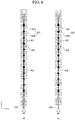
- FIG. 6 , (a) and (b) are front plan views illustrating enlarged views of a part A and a part B of FIG. 5
- FIG. 7 is a cross-sectional view taken along a line VII-VII of FIG. 1 .
- FIGS. 7 to 9 schematically illustrate the shapes of the solar cell 150 and the wiring member 142.
- each of solar cell strings OS1, OS2, and IS includes a plurality of solar cells 150 and a plurality of wiring members 142 connecting the plurality of solar cells 150 in first direction (an extension direction, a second direction), respectively.
- the solar cell strings OS1, OS2, and IS can be provided in a plurality so as to be spaced apart from each other in a direction (the second direction, the first direction) intersecting with first direction.
- the plurality of solar cell strings OS1, OS2, and IS can include a first solar cell string (a first outer solar cell string, OS1) positioned at a first edge 101 of the solar panel 100 in the second direction and a second solar cell string (a second outer solar cell string, OS2) positioned to be adjacent to a second edge 102 of the solar panel 100 opposite the first edge 101 in the second direction, and can further include an inner solar cell string IS positioned between the first and second solar cell strings OS1, OS2.
- a plurality of wiring members 142 positioned in at least one of first and second solar cells 151 and 152 included in the first and second solar cell strings OS1 and OS2 and a third solar cell 153 included in the inner solar cell string IS include a first wiring member 1421 having a first width (or a first diameter, W1) and a second wiring member 1422 having a second width (or a second diameter, W2) less than the first width W1 and positioned outside or outer to the first wiring member 1421.
- the solar cell 150 including the first and second wiring members 1421 and 1422 can be used as at least one of the first to third solar cells 151, 152, and 153.
- the second wiring member 1422 can be positioned to be adjacent to a first side of the first solar cell 151 adjacent to at least the first edge 101.
- the second wiring member 1422 can be positioned adjacent to a second side of the second solar cell 152 adjacent to at least the second edge 102. Then, the second wiring member 1422 having a small width (or diameter) is positioned at positions adjacent to the first and second edges 101, 102 of the solar panel 100, which are parts in which the thickness of the sealing member 130 can be reduced during the lamination process.
- the wiring member 142 includes a circular or rounded part, and/or has a relatively large thickness (a thickness substantially equal to the width, for example, a thickness of 80% to 120% of the width, or a thickness of 1 mm or less) compared to the width (for example, 1 mm or less), or the first and second cover members 110 and 120 each have a glass substrate.
- the first and second cover members 110 and 120 each include the glass substrate, and a ratio of the thickness of the sealing member 130 (that is, the first or second sealing member 131 and 132) positioned on one side of the solar cell 150 to the first width W1 of the relatively large first wiring member 1421 can be two times or less.
- the thickness (that is, a thickness of the first or second sealing member 131 and 132) of the sealing member 130 positioned on one side of the solar cell 150 can mean a thinnest thickness as a distance between the solar cell 150 and the first or second cover member 110 and 120.
- the first or second sealing member 131, 132 are difficult to be made to have a predetermined thickness or more, in order to increase the thickness, the first or second sealing member 131, 132 must be provided in a plurality of layers to form one first or second sealing member 131 and 132, the process cost can increase significantly, and accordingly, the thickness and weight of the solar panel 100 can also increase significantly. Accordingly, in the present embodiment, the first or second sealing member 131, 132 can be formed to have a predetermined thickness or less to reduce the number or thickness of layers constituting the sealing member 130.
- the ratio of the second width W2 of the second wiring member 1422 to the first width W1 of the first wiring member 1421 can be 0.5 or more (for example, 0.5 to 0.95). More specifically, the ratio of the second width W2 of the second wiring member 1422 to the first width W1 of the first wiring member 1421 can be 0.6 to 0.9.
- the first width W1 of the first wiring member 142 can be 200 to 500 ⁇ m.
- the plurality of solar cells 150 can be electrically connected to each other stably by the first and second wiring members 1421 and 1422, and the effect by the second wiring member 1422 can be effectively exhibited.
- the number of second wiring members 1422 can be less than the number of first wiring members 1421 when viewed on one surface of the solar cell 150 including the first and second wiring members 1421 and 1422.
- the number of first wiring members 1421 is greater than the number of second wiring members 1422 so that carriers can be stably transmitted, and the second wiring members 1422 can be positioned in a less number only in necessary parts.
- each second wiring member 1422 is positioned on both sides of the first and second solar cells 151 and 152, and a plurality of first wiring members 1421 are positioned inside the second wiring member 1422 positioned on the both sides.
- each of the third solar cells 153 positioned on the inner solar cell string IS also has one second wiring member 1422 on both sides thereof, and the plurality of first wiring members 1421 can be positioned inside the second wiring members 1422 positioned on the both sides.
- the solar cell strings OS1, OS2, and IS that include the plurality of solar cells 150 connected to each other so that each of the second wiring member 1422 is positioned on the both sides thereof and the first wiring member 1421 is positioned therein, they can be connected with the bus ribbon 145 or the like. Then, in manufacturing the solar panel 100, the first to third solar cells 151, 152 and 153 or the first and second solar cell strings OS1 and OS2 and the inner solar cell string IS are not distinguished, so that the manufacturing process can be simplified.
- the present invention is not limited thereto.
- a plurality of second wiring members 1422 can be provided when viewed from one side.
- the second wiring member 1422 in the first solar cell 151, can be provided in a plurality in a region S1 from the first side of the first solar cell 151 to 15% of a width of the first solar cell 151 along the second direction.
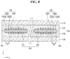
- the plurality of second wiring members 1422 positioned on one side of the first solar cell 151 can have the same width or diameter as each other, or as shown in FIG. 8 , the plurality of second wiring members 1422a and 1422b can be positioned to be less in width or diameter as they are adjacent to the first side.
- the second wiring member 1422 can be provided in a plurality in a region S2 from the second side of the second solar cell 152 to 15% of a width of the second solar cell 152 along the second direction.
- the plurality of second wiring members 1422 positioned on one side of the second solar cell 152 can have the same width or diameter as each other, or as shown in FIG. 8 , the plurality of second wiring members 1422a and 1422b can be positioned to be less in width or diameter as they are adjacent to the second side.
- the second wiring members 1422 are positioned at both sides of the first to third solar cells 151, 152, and 153, and the width, diameter, number, and the like of the second wiring members 1422 positioned on the both sides are symmetrical to each other. Accordingly, although the first to third solar cells 151, 152, and 153 can have a symmetrical structure to have structural stability, the present invention is not limited thereto.
- one or a plurality of second wiring members 1422 are positioned only at a part adjacent to the first side, and the first wiring member 1421 can be positioned in the remaining part, so the first wiring member 1421 can be positioned instead of the second wiring member 1422 on the second side.
- the second solar cell 152 one or a plurality of second wiring members 1422 are positioned only at a part adjacent to the second side, and the first wiring member 1421 can be positioned in the remaining part, so the first wiring member 1421 can be positioned instead of the second wiring member 1422 on the first side.
- the second wiring member 1422 can be positioned only at a part where the second wiring member 1422 having a relatively small width should be positioned to increase the number of the first wiring members 1421, thereby stably transmitting the carriers.
- the second wiring member 1422 is positioned on the first side and the second side, respectively, but the width, diameter, number, etc. of the second wiring members 1422 can be different from each other on the first side and the second side. Many other variations are possible.
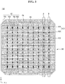
- the first and second solar cells (see reference numerals 151 and 152 of FIGS. 7 to 9 ) included in the first and second solar cell strings OS1 and OS2 can form a first region A1 including the first wiring member 1421 and the second wiring member 1422 together, and the third solar cell 153 included in the inner solar cell string IS can form a second region A2 that does not include the second wiring member 1422, but includes only the plurality of first wiring members 1421 having substantially the same width.
- the carrier can be stably transmitted by positioning the first wiring member 1421 only in the first region A1 where a problem such as disconnection of the wiring member 142 is likely to occur.
- FIG. 11 schematically illustrates the third solar cell 153 and the wiring member 142.
- the pads 422 corresponding to the first and second wiring members 1421 and 1422 have substantially the same shape.
- the present invention is not limited thereto.
- the number, area (for example, the length), etc. of the pad part 422 corresponding to the second wiring member 1422 can be greater than the number, area (for example, the length), etc. of the pad part 422 corresponding to the first wiring member 1421.
- the number, area (for example, the length), etc. of the pad part 422 corresponding to the first wiring member 1421 can be greater than the number, area (for example, the length), etc.
- a length of each of the first outer pad 424 and the first inner pad 426 corresponding to the second wiring member 1422 is longer than a length of each of the first outer pad 424 and the first inner pad 426 corresponding to the first wiring member 1421.
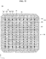
- the second wiring members 1422 are provided on the first and second sides of the solar cell 150, respectively, it is illustrated that the number, area, etc. of the pad part 422 of the first bus bar 42b adjacent to each of the first and second sides are different from the number, area, etc. of the first pad part 422 of the first bus bar 42b positioned therein.
- the present invention is not limited thereto, and the length of at least one of the first outer pad 424 and the first inner pad 426 corresponding to the second wiring member 1422 can be longer than the length of at least one of the first outer pad 424 and the first inner pad 426 corresponding to the first wiring member 1421.
- the number of first pads 422 corresponding to the second wiring members 1422 can be greater than the number of first pads 422 corresponding to the first wiring members 1421.
- the first electrode 42 is illustrated as an example, at least one of the first and second electrodes 42 and 44 can have the above-described structure.
- the position, number, etc. of the bus bars 42b positioned in the first pad part 422 which differs in number, area, etc. according to the position, number, etc. of the second wiring member 1422 can also vary.
- the number, area, etc. of the first pad part 422 corresponding to the second wiring member 1422 which can reduce the attachment characteristics due to a small width, are greater than the number, area, etc. of the first pad part 422 corresponding to the first wiring member 1421, so that the fall of the attachment characteristics of the wiring member 1422 can be prevented.
- the present invention is not limited thereto. Accordingly, the number, area, etc. (for example, length, width, etc.) of the first pads 422 corresponding to the second wiring member 1422 can be less than the number, area, etc. (for example, length, width, etc.) of the first pad part 422 corresponding to the first wiring member 1421. Many other variations are possible.
- each of the above structures is applied, and the effect of the second wiring member 1422 can be greatly improved in the plurality of first solar cells 151 included in the first solar cell string OS1 and the plurality of second solar cells 152 included in the second solar cell string OS2.
- the present invention is not limited thereto. Even when the above-mentioned second wiring member 1422 is positioned only in at least one of the plurality of first solar cells 151 or at least one of the plurality of second solar cells 152, it is within the scope of the present invention.
- At least one of the plurality of first to third solar cells 151, 152, and 153 includes the first wiring member 1411 having the first width W1 and the second wiring member 1422 positioned outside the first width W1 and having the second width W2 less than the first width W1, so that the problems that can occur at the edge parts of the first, second, or third solar cells 151, 152, and 153 can be effectively prevented. Accordingly, this also belongs to the scope of the present invention.
- the problems such as damage and disconnection of the wiring member 142 that can occur at the edges 101 and 102 of the solar panel 100 can be prevented by a simple structure in which the first wiring member 1421 and the second wiring member 1422 are positioned.
- the long-term reliability of the solar panel 100 can be improved while the solar panel 100 is manufactured by a simple process.
- This effect can be especially doubled in a structure in which the thickness of the sealing member 130 is below a certain level, the wiring member 142 includes a circular shape or rounded part or has a relatively large thickness compared to the width, or the first and second cover members 110 and 120 each have a glass substrate.
Landscapes
- Photovoltaic Devices (AREA)
- Engineering & Computer Science (AREA)
- Life Sciences & Earth Sciences (AREA)
- Sustainable Development (AREA)
- Sustainable Energy (AREA)
- Microelectronics & Electronic Packaging (AREA)
Description
- Embodiments of the invention relate to a solar cell panel, and more particularly, to a solar cell panel having an improved structure.
- A plurality of solar cells are connected by ribbons, interconnectors, and the like, and are protected by sealing members and cover members to produce solar cell panels. As a result, the solar cell panels can have desired outputs and can be safely protected even when exposed to an external environment for a long period of time. For example,
US 2016/0093752 A1 discloses a plurality of solar cells which are electrically interconnected in series by a plurality of leads thereby forming a solar cell string of a solar cell panel. - The solar cell panels including the various members are integrated by a lamination process for applying heat and pressure. A part that receives a large load due to the pressure applied during the lamination process can have characteristics different from those of other parts, so that when the solar cell panels are used for a long period of time, undesirable problems can occur in the part. These problems can be more serious when the cover members constituting both outer surfaces of the solar panel are composed of a glass substrate and a larger pressure is provided.
- For example, in the case where each of the cover members forming the both outer surfaces of the solar cell panel is composed of a glass substrate, the thickness of the sealing members at the edges of the solar cell panel is reduced by the weight of the cover member during the lamination process. When a thermal cycle test in which the temperature is repeatedly changed in the solar cell panel is performed, problems such as damage or disconnection of the ribbon, the interconnector, and the like can be caused at the edge of the solar cell panel where the relatively thin sealing members are positioned. These problems can occur more seriously when the thickness of the ribbon, the interconnector, etc. is relatively large in comparison with the width.
- An object of the present invention is to provide a solar cell panel capable of improving long-term reliability with a simple structure.
- In particular, the present invention is intended to provide a solar cell panel capable of preventing damage or disconnection of wiring members which can occur when a front cover member and a back cover member are composed of a glass substrate and the wiring members including a relatively large thickness compared to its width or a circular shape or a rounded part are used. The invention provides a solar cell panel according to
claim 1. - A solar cell panel according to an embodiment of the present invention includes a solar cell string including a plurality of solar cells and a plurality of wiring members connecting the plurality of solar cells in first direction, a sealing member sealing the solar cell string, a first cover member positioned on one surface of the solar cell string on the sealing member, a second cover member positioned on other surface of the solar cell string on the sealing member, wherein the plurality of wiring members positioned in at least one of the plurality of solar cells include, a first wiring member having a first width, a second wiring member having a second width less than the first width and positioned outside the first wiring member.
- The solar cell string includes a first solar cell string positioned close to a first edge of the solar cell panel in an second direction intersecting the first direction and a second solar cell string positioned close to a second edge of the solar cell panel in the second direction,
- In at least one of a plurality of first solar cells included in the first solar cell string, the second wiring member is positioned close to a first side of a first solar cell adjacent to the first edge, and wherein in at least one of a plurality of second solar cells included in the second solar cell string, the second wiring member is positioned close to a second side of a second solar cell adjacent to the second edge.
- In the first solar cell, the second wiring member can be provided in one or a plural in a region from the first side to about 15% of a width of the first solar cell along the second direction, and wherein in the second solar cell, the second wiring member can be provided in one or a plural in a region from the second side to about 15% of a width of the second solar cell along the second direction.
- A ratio (w2/w1) of the second width (w1) of the second wiring member to the first width (w1) of the first wiring member can be about 0.5 or more.
- The ratio (w2/w1) of the second width (w2) of the second wiring member to the first width (w1) of the first wiring member can be about 0.6 to 0.9.
- The first width of the first wiring member can be about; 200 µm to 500 µm, or the first or second wiring member has a circular or rounded part.
- A number of the second wiring member can be less than a number of the first wiring member.
- A thickness of the sealing member positioned on one side of the solar cell panel can be two times or less with respect to the first width of the first wiring member.
- Each of the first and second cover members includes a glass substrate.
- In the first and second solar cells, the second wiring member can be positioned to be adjacent to the first side of the first solar cell and the second side of the second solar cell, and is not positioned to be adjacent to a second side of the first solar cell and a first side of the second solar cell, or in the first and second solar cells, the second wiring member can be positioned to be adjacent to the first side and the second side of the first solar cell and the first side and the second side of the second solar cell, respectively.
- The solar cell string further can include at least one inner solar cell string positioned between the first solar cell string and the second solar cell string, and the second wiring member can be provided in the first and second solar cell strings, and the second wiring member is not provided in the inner solar cell string.
- Each of the first and second solar cells can include a semiconductor substrate, a conductive type region positioned in one surface of the semiconductor substrate or on the one surface of the semiconductor substrate, an electrode electrically connected to the conductive type region, wherein the electrode includes a plurality of finger lines parallel to each other, a plurality of bus bars respectively including a plurality of pads electrically connected to the plurality of finger lines and positioned along a direction intersecting the finger lines, and wherein at least one of a size and a number of the plurality of pads of the bus bar corresponding to the second wiring member is greater than a size and a number of the plurality of pads of the bus bar corresponding to the first wiring member.
- According to the present embodiment, it is possible to prevent problems such as damage and disconnection of the wiring members that can occur at the edges of the solar cell panel by a simple structure using the wiring members having different widths. Thereby, the long-term reliability of the solar cell panel can be improved while manufacturing the solar cell panel by a simple process. This effect can be particularly doubled in a structure in which the thickness of the sealing member is below a certain level, the wiring member includes a circular shape or a rounded part, the wiring member has a relatively large thickness as compared with the width, or the first and second cover members each include a glass substrate.
-
-
FIG. 1 is a perspective view illustrating a solar cell panel according to an embodiment of the present invention. -
FIG. 2 is a cross-sectional view taken along a line II-II inFIG. 1 . -
FIG. 3 is a partial cross-sectional view illustrating a solar cell and a wiring member connected thereto which are included in a solar cell panel shown inFIG. 1 . -
FIG. 4 is a perspective view schematically illustrating two neighboring solar cells which are included in a solar cell panel shown inFIG. 1 and connected by a wiring member. -
FIG. 5 is a front plan view of a solar cell shown inFIG. 4 . -
FIG. 6 includes (a) and (b) that are front plan views illustrating enlarged views of a part A and a part B ofFIG. 5 . -
FIG. 7 is a cross-sectional view taken along the line VII-VII ofFIG. 1 . -
FIG. 8 is a cross-sectional view of a solar cell panel according to a modification of the present invention. -
FIG. 9 is a cross-sectional view of a solar cell panel according to another modification of the present invention. -
FIG. 10 is a plan view schematically illustrating a solar cell panel according to another embodiment of the present invention. -
FIG. 11 is a cross-sectional view illustrating a third solar cell provided in a second region of a solar cell panel illustrated inFIG. 10 . -
FIG. 12 is a front plan view of a solar cell included in a solar cell panel according to another embodiment of the present invention. - Hereinafter, embodiments of the present invention will be described in detail with reference to the accompanying drawings. However, it is needless to say that the present invention is not limited to these embodiments and can be modified into various forms.
- In the drawings, illustration of the parts not related to the description is omitted in order to clarify and briefly describe the present invention, and the same reference numerals are used for the same or very similar parts throughout the specification. In the drawings, the thickness, width, and the like are enlarged or reduced to make the explanation more clear, and the thickness, width, etc. of the present invention are not limited to those shown in the drawings.
- When a part is referred to as "including" another part throughout the specification, it does not exclude other parts and can further include other parts unless specifically stated otherwise. Further, when a part of a layer, a film, a region, a plate, or the like is referred to as being "on" other part, this includes not only the case where it is "directly on" the other part but also the case where the other part is positioned in the middle. When the part of the layer, the film, the region, the plate, or the like is referred to as being "directly on" the other part, it means that no other part is positioned in the middle.
- Hereinafter, a solar cell and a solar cell panel including the solar cell according to an embodiment of the present invention will be described in detail with reference to the accompanying drawings. In the following, the expressions "first", "second", "third", etc. are used only to distinguish each other, but the present invention is not limited thereto.
-
FIG. 1 is a perspective view illustrating a solar cell panel according to an embodiment of the present invention, andFIG. 2 is a cross-sectional view taken along a line II-II inFIG. 1 . - Referring to
FIGS. 1 and2 , asolar cell panel 100 according to the present embodiment includes a plurality ofsolar cells 150 and a wiring member (or a wire, an interconnector, etc.) 142 for electrically connecting the plurality ofsolar cells 150 in first direction. Thesolar cell panel 100 includes asealing member 130 that surrounds and seals the solar cell strings OS1, OS2 and IS, afirst cover member 110 positioned on a front surface of the solar cell strings OS1, OS2 and IS on thesealing member 130, and asecond cover member 120 positioned on a back surface of the solar cell strings OS1, OS2 and IS on the sealingmember 130. This will be explained in more detail. - First, the
solar cell 150 can include a photoelectric conversion unit that converts the solar cell into electric energy, and an electrode that is electrically connected to the photoelectric conversion unit to collects and transfers a current. The plurality ofsolar cells 150 can be electrically connected in series, parallel, or series-parallel by thewiring member 142. Specifically, thewiring member 142 electrically connects two neighboringsolar cells 150 among the plurality ofsolar cells 150. - A
bus ribbon 145 alternately connects two ends of thewiring member 142 of the solar cell 150 (i.e., the solar cell string OS1, OS2 and IS) connected by thewiring material 142 to form one row. Thebus ribbon 145 can be positioned at an end of the solar cell string OS1, OS2 and IS in a direction intersecting the end. Thisbus ribbon 145 can connect the solar cell strings OS1, OS2 and IS adjacent to each other, or can connect the solar cell string OS1, OS2 and IS to a junction box (not shown) that prevents reverse flow of the current. The material, shape, connection structure, etc. of thebus ribbon 145 can be variously modified, and the present invention is not limited thereto. - The sealing
member 130 can include afirst sealing member 131 positioned on the front surface of thesolar cell 150 connected by thewiring member 142, and asecond sealing member 132 positioned on the back surface of thesolar cell 150. Thefirst sealing member 131 and thesecond sealing member 132 prevent moisture and oxygen from entering and chemically bind each element of thesolar cell panel 100. The first andsecond sealing members first sealing member 131 and thesecond sealing member 132. Thesecond cover member 120, thesecond sealing member 132, thesolar cell 150, thefirst sealing member 131, and thefirst cover member 110 are integrated to form thesolar cell panel 100 by a lamination process or the like using the first andsecond sealing members - The
first cover member 110 is positioned on thefirst sealing member 131 to constitute the front surface of thesolar cell panel 100, and thesecond cover member 120 is positioned on thesecond sealing member 132 to constitute the back surface of thesolar cell panel 100. Thefirst cover member 110 and thesecond cover member 120 can be made of an insulating material capable of protecting thesolar cell 150 from external shock, moisture, ultraviolet rays, or the like. For example, in this embodiment, each of the first andsecond cover members solar cell panel 100 can improve the output. - However, the present invention is not limited thereto. Accordingly, the first and
second sealing members - The
solar cell 150 and thewiring member 142 connected thereto according to the embodiment of the present invention will be described in more detail with reference toFIG. 3. FIG. 3 is a partial cross-sectional view illustrating thesolar cell 150 and thewiring member 142 connected thereto which are included in thesolar cell panel 100 shown inFIG. 1 . For simplicity,electrodes FIG. 3 . - Referring to
FIG. 3 , thesolar cell 150 includes asemiconductor substrate 160,conductive type regions semiconductor substrate 160, andelectrodes conductive type regions conductive type regions conductive type region 20 having a first conductive type and a secondconductive type region 30 having a second conductive type. Theelectrodes first electrode 42 connected to the firstconductive type region 20 and asecond electrode 44 connected to the secondconductive type region 30. Furthermore, thesolar cell 150 can further include first and second passivation layers 22 and 32, ananti-reflection layer 24, and the like. - The
semiconductor substrate 160 can be composed of a crystalline semiconductor (for example, a single crystal or polycrystalline semiconductor, for example, a single crystal or polycrystalline silicon) including a single semiconductor material (for example, a group 4 element). Then, since thesemiconductor substrate 160 having a high degree of crystallinity and having few defects is used as a base, thesolar cell 150 can have excellent electrical characteristics. - The front surface and/or the back surface of the
semiconductor substrate 160 can be textured to have unevenness. The unevenness can have, for example, a pyramid shape having an irregular size, whose outer surface is composed of the plane (111) of thesemiconductor substrate 160. As a result, the reflectance of light can be reduced if having a relatively large surface roughness. However, the present invention is not limited thereto. - In this embodiment, the
semiconductor substrate 160 includes abase region 10 having the first or second conductive type by doping a first or second conductive type dopant with a lower doping concentration than the first or secondconductive type region base region 10 can have the second conductive type in this embodiment. - As an example, the first
conductive type region 20 can constitute an emitter region that forms a p-n junction with thebase region 10. The secondconductive type region 30 can form a back surface field to form a back field region for preventing recombination. Here, the first and secondconductive type regions semiconductor substrate 160. Thus, the first and secondconductive type regions - In this embodiment, the
base region 10 and theconductive type regions semiconductor substrate 160 are exemplified as regions having a crystal structure of thesemiconductor substrate 160 and different conductive type, doping concentration. That is, it is illustrated that theconductive type regions semiconductor substrate 160. However, the present invention is not limited thereto. Therefore, at least one of the firstconductive type region 20 and the secondconductive type region 30 can be formed of an amorphous, microcrystalline or polycrystalline semiconductor layer or the like, which is formed on thesemiconductor substrate 160 as a separate layer. Other variations are possible. - The first conductive type dopant included in the first
conductive type region 20 can be an n-type or p-type dopant, and the second conductive type dopant included in thebase region 10 and the secondconductive type region 30 can be a p-type or n-type dopant. Group 3 elements such as boron (B), aluminum (Al), gallium (Ga), or indium (In) can be used as the p-type dopant, and group 5 elements such as phosphorus (P), arsenic (As), bismuth (Bi), and antimony (Sb) can be used as the n-type dopant. The second conductive type dopant in thebase region 10 and the second conductive type dopant in the secondconductive type region 30 can be the same material or different materials. - For example, the first
conductive type region 20 can have a p-type, thebase region 10 and the secondconductive type region 30 can have an n-type. Then, holes having a slower moving speed than electrons can move to the front surface of thesemiconductor substrate 160, rather than the back surface thereof, thereby improving the conversion efficiency. However, the present invention is not limited thereto, and the opposite case is also possible. - An insulating layer such as the first and second passivation layers 22 and 32 for immobilizing defects of the
conductive type regions anti-reflection layer 24 for preventing reflection of light can be formed on the surface of thesemiconductor substrate 160. Such an insulating layer can be composed of an undoped insulating layer which does not contain a dopant separately. The first and second passivation layers 22 and 32 and theanti-reflection layer 24 can be formed substantially entirely on the front surface and back surface of thesemiconductor substrate 160 except for parts (more precisely, parts where a first or second opening is formed) corresponding to the first orsecond electrode - For example, the first or
second passivation layer anti-reflection layer 24 can have a silicon nitride layer, a silicon nitride layer containing hydrogen, a silicon oxide layer, a silicon oxynitride layer, an aluminum oxide layer, any one single layer selected from a group consisting of MgF2, ZnS, TiO2 and CeO2 or a multi-layered structure in which two or more layers are combined. For example, the first orsecond passivation layer conductive type region conductive type region anti-reflection layer 24 can include silicon nitride. In addition, the material of the insulating layer, the multi-layered structure, and the like can be variously modified. - The
first electrode 42 is electrically connected to the firstconductive type region 20 through a first opening and thesecond electrode 44 is electrically connected to the secondconductive type region 30 through a second opening. The first andsecond electrodes second electrodes - As described above, in this embodiment, since the first and
second electrodes solar cell 150 have a certain pattern, thesolar cell 150 has a bi-facial structure in which light can be incident on the front surface and the back surface of thesemiconductor substrate 160. Accordingly, the amount of light used in thesolar cell 150 can be increased to contribute to the efficiency improvement of thesolar cell 150. - However, the present invention is not limited thereto, and it is also possible that the
second electrode 44 is formed entirely on the back surface of thesemiconductor substrate 160. It is also possible that the first and secondconductive type regions second electrodes semiconductor substrate 160, and it is also possible that at least one of the first and secondconductive type regions semiconductor substrate 160. That is, thesolar cell 150 described above is merely an example, and the present invention is not limited thereto. - The
solar cell 150 described above is electrically connected to the neighboringsolar cell 150 by thewiring member 142 positioned (e.g., in contact with) on thefirst electrode 42 or thesecond electrode 44, and this will be described in more detail with reference toFIG. 4 together withFIG. 1 to FIG. 3 . -
FIG. 4 is a perspective view schematically illustrating two neighboringsolar cells 150a, 150b which are included in thesolar cell panel 100 shown inFIG. 1 and connected by thewiring member 142. InFIG. 4 , the two neighboringsolar cells 150a, 150b are schematically shown mainly on thesemiconductor substrate 160 and theelectrodes - As shown in
FIGS. 1 to 4 , thewiring member 142 connects thefirst electrode 42 positioned on a front surface of one solar cell 150a and thesecond electrode 44 positioned on a back surface of neighboringsolar cell 150b positioned at one side (lower left of the drawing) of the one solar cell 150a. Anotherwiring member 142 connects thesecond electrode 44 positioned on the back surface of the one solar cell 150a and thefirst electrode 42 positioned on the front surface of another solar cell to be positioned on another side (upper right of the drawing) of the one solar cell 150a.Other wiring member 142 connects thefirst electrode 42 positioned on the front surface of the neighboringsolar cell 150b and thesecond electrode 44 positioned on the back surface of other solar cell to be positioned at one side (lower left of the drawing) of the neighboringsolar cell 150b. Accordingly, the plurality ofsolar cells 150 can be connected to each other by thewiring member 142 to form one row. Hereinafter, the description of thewiring member 142 can be applied to all thewiring member 142 connecting two neighboringsolar cells 150. - At this time, the plurality of
wiring members 142 can be extended to be positioned along first direction (an x-axis direction in the drawing, a direction intersecting a first finger line (reference numeral 42a inFIG. 5 , hereafter the same), or an extending direction of a first bus bar (reference numeral 42b inFIG. 5 hereafter the same)) on one surface of eachsolar cell 150 to improve electrical connection characteristics of neighboringsolar cells 150. - In this embodiment, the
wiring member 142 can be formed of a wire having a width smaller than that of a ribbon having a relatively wide width (for example, more than 1 mm) which has been used conventionally. For example, a maximum width of thewiring member 142 can be 1 mm or less (for example, 500 µm or less). Here, the maximum width of thewiring member 142 can mean a largest width among widths passing the center of thewiring member 142. When thewiring member 142 has such a maximum width, it can be smoothly attached to thesolar cell 150 while the resistance of thewiring member 142 can be kept low and the optical loss can be minimized. - The number of the
wiring members 142 can be greater than the number (for example, 2 to 5) of the conventional ribbons on the basis of one surface of eachsolar cell 150. Then, a movement distance of carriers can be reduced by a large number of thewiring members 142 while minimizing the optical loss and material cost by thewiring member 142 having a small width. Thus, the efficiency of thesolar cell 150 and the output of thesolar cell panel 100 can be improved by reducing the movement distance of the carriers while reducing the optical loss, and productivity of thesolar cell panel 100 can be improved by reducing the material cost due to thewiring member 142. - In order to prevent the process of attaching the
wiring member 142 to thesolar cell 150 from becoming complicated when the number of thewiring member 142 having the small width is used in a large number, in this embodiment, thewiring member 142 can have a structure including acore layer 142a and asolder layer 142b formed on the surface of thecore layer 142a. Then, a large number of thewiring member 142 can be effectively attached by the process of applying heat and pressure while thewiring member 142 is placed on thesolar cell 150. - The
wiring member 142 or thecore layer 142a, which is included in thewiring material 142 and occupies most of thewiring member 142, can include rounded parts. That is, at least a part of the cross section of thewiring member 142 or thecore layer 142a can include a circle, a part of a circle, an ellipse, a part of an ellipse, or a part made of a curve. - If it has such a shape, the
wiring member 142 is formed in a structure in which thesolder layer 142b is entirely positioned on the surface of thecore layer 142a, the process of separately applying the solder material and the like are omitted, so that thewiring member 142 can be attached by positioning thewiring member 142 directly on thesolar cell 150. Thus, the process of attaching thewiring member 142 can be simplified. In addition, light reflected by thewiring member 142 can be re-incident on thesolar cell 150 and reused by being reflected or diffused by the rounded parts of thewiring member 142. Accordingly, since the amount of light incident on thesolar cell 150 is increased, the efficiency of thesolar cell 150 and the output of thesolar cell panel 100 can be improved. However, the present invention is not limited thereto. Therefore, the wire constituting thewiring member 142 can have a polygonal shape such as a quadrangle, or can have various other shapes. - At this time, the number of the
wiring members 142 can be 6 to 33 (for example, 8 to 33, for example, 10 to 33, particularly 10 to 15), and they can be spaced apart from each other at a uniform distance. The plurality of thewiring member 142 in eachsolar cell 150 can have a symmetrical shape when viewed in an extending direction of thefirst finger line 42a. Thus, a sufficient number of thewiring members 142 can be provided, and the movement distance of the carriers can be minimized. - In this embodiment, the
wiring member 142 can include thecore layer 142a made of metals and thesolder layer 142b that is formed on the surface of thecore layer 142a and includes solder material to enable soldering with theelectrodes solder layer 142b can serve as a kind of adhesive layer. For example, thecore layer 142a can include Ni, Cu, Ag, Al, or the like as a main material (for example, a material containing 50 wt% or more, more specifically, a material containing 90 wt% or more). Thesolder layer 142b can include a solder material such as Pb, Sn, SnIn, SnBi, SnPb, SnPbAg, SnCuAg, SnCu, or the like as a main material. However, the present invention is not limited thereto, and thecore layer 142a and thesolder layer 142b can include various materials. - On the other hand, when the
wiring member 142 is attached to thesolar cell 150 by a tabbing process, as shown inFIG. 3 , a shape of thesolder layer 142b is changed in a part of thewiring member 142 attached to or connected to thesolar cell 150. - More specifically, the
wiring member 142 is attached to atleast pads 422 and 442 by thesolder layer 142b. At this time, thesolder layer 142b of eachwiring member 142 is separately positioned withother wiring member 142 orsolder layer 142b. When thewiring member 142 is attached to thesolar cell 150 by the tabbing process, eachsolder layer 142b flows down to the first orsecond electrodes 42, 44 (more specifically, thepads 422 and 424) as a whole during the tabbing process, and a width of thesolder layer 142b can gradually increase toward thepads 422, 442 at a part adjacent to eachpad part 422, 442 or a part positioned between thepads 422, 442 and thecore layer 142a. As one example, the part adjacent to thepads 422 and 442 in thesolder layer 142b can have a width equal to or greater than a diameter of thecore layer 142a. At this time, the width of thesolder layer 142b can be equal to or less than a width of thepads 422, 442. - More specifically, the
solder layer 142b has a shape protruding toward the outside of thesolar cell 150 along the shape of thecore layer 142a in an upper part of thecore layer 142a. On the other hand, thesolder layer 142b includes a part having a concave shape with respect to the outside of thesolar cell 150 in a lower part of thecore layer 142a or a part adjacent to thepads 422 and 442. As a result, an inflection point where the curvature changes is positioned on the side of thesolder layer 142b. It can be seen that thewiring member 142 are individually attached and fixed by thesolder layer 142b without being inserted or covered in a separate layer, film, or the like from this shape of thesolder layer 142b. Thesolar cell 150 and thewiring member 142 can be connected by a simple structure and a process by fixing thewiring member 142 by thesolder layer 142b without using a separate layer or a film. Particularly, thewiring member 142 having a narrow width and a rounded shape as in the present embodiment can be attached without using a separate layer, a film, (for example, a conductive adhesive film including a resin and a conductive material) or the like, so that the process cost and time of thewiring member 142 can be minimized. - On the other hand, the part of the
wiring member 142 positioned between the neighboring solar cells 150 (that is, outside the solar cell 150), which is not applied with heat or is applied with relatively less heat even after the tabbing process, can have a shape in which thesolder layer 142b has a uniform thickness as shown inFIG. 4 . - According to the present embodiment, optical loss can be minimized by diffused reflection or the like using a wire-shaped
wiring material 142, and it is possible to reduce the movement path of the carrier by increasing the number of thewiring member 142 and reducing a pitch of thewiring member 142. In addition, the width or diameter of thewiring member 142 can be reduced, so that the material cost can be greatly reduced. Accordingly, the efficiency of thesolar cell 150 and the output of thesolar cell panel 100 can be improved. - Referring to
FIG. 5 withFIGS. 1 to 4 , an example of theelectrodes solar cell 150 to which thewiring member 142 according to an embodiment of the present invention is attached will be described in detail. Hereinafter, with reference toFIG. 5 thefirst electrode 42 will be described in detail, and for thesecond electrode 44, the same or similar parts as thefirst electrode 42 and the different parts from thefirst electrode 42 will be described. -
FIG. 5 is a front plan view of thesolar cell 150 shown inFIG. 4 . - Referring to
FIGS. 1 to 5 , in this embodiment, thefirst electrode 42 includes a plurality offirst finger lines 42a being extended in a first direction (an y-axis direction in the drawing) and positioned parallel to each other, and afirst bus bar 42b formed in a second direction (an x-axis direction in the drawing) intersecting (for example, orthogonal) with thefirst finger line 42a and electrically connected to thefirst finger line 42a and connected or attached to thewiring member 142. In the drawing, it is further formed arim line 42c that connects the ends of the plurality offirst finger lines 42a as a whole in the vicinity of both side edges. Therim line 42c can have the same or similar width as thefirst finger line 42a and can be composed of the same material as thefirst finger line 42a. However, it is also possible not to include therim line 42c. - At this time, in this embodiment, the solar cell 150 (or the semiconductor substrate 160) can be partitioned into an electrode area EA and an edge area PA. Here, the electrode area EA can be an area in which the
first finger lines 42a formed in parallel to each other are arranged at a uniform pitch. The electrode area EA can include a plurality of electrode areas EA partitioned by thewiring member 142. The edge area PA is an area positioned between two adjacent electrode areas EA and positioned adjacent to an edge of thesemiconductor substrate 160 or thesolar cell 150 outside a plurality of first pad part 422 (particularly, first outer pads 424). At this time, the edge area PA can be an area where anelectrode part 42d is positioned at a density lower than a density of thefirst finger line 42a of the electrode area EA, or an area where theelectrode part 42d is not positioned. In the drawing, it is illustrated that theelectrode parts 42d positioned on both sides of each other have the same shape. However, the present invention is not limited thereto, and various other modifications are possible. - In this embodiment, at least a part of the plurality of
first finger lines 42a include a contact part which is in direct contact with the firstconductive type region 20, and serve to collect carriers generated by the photoelectric conversion from the firstconductive type region 20. In one example, the plurality offirst finger lines 42a can be extended in parallel to each other and spaced apart from each other so as to have a constant pitch. - In this embodiment, the
first bus bar 42b can include the plurality offirst pad part 422 positioned in the second direction and can further include afirst line part 421 which is elongated with a relatively narrow width along a direction in which thewiring member 142 is connected. Thefirst pad part 422 can improve the adhesion with thewiring member 142 and reduce the contact resistance, and thefirst line part 421 can minimize the optical loss. Thefirst line part 421 can provide a path through which the carrier can bypass when some of thefirst finger lines 42a are broken. Thewiring material 142 can be attached to thefirst line part 421, or thewiring member 142 can be placed on thefirst line part 421 in a state where thewiring member 142 is not attached to thefirst line part 421. - More specifically, the plurality of
first pads 422 includes theouter pad 424 positioned to be adjacent to the edge of thesemiconductor substrate 160 in the second direction, and aninner pad 426 positioned inside the outer pad. Here, theouter pad 424 can mean two pads positioned to be closest to each of the two side edges when viewed in the second direction among the plurality offirst pads 422, and the firstinner pad 426 can mean a pad positioned between two firstouter pads 424. Here, since the outer/inner reference is based on only the plurality offirst pads 422, unlike the drawing, thefirst line part 421 can be positioned outside the firstouter pad 424. - A width of the
first pad part 422 in the first direction can be greater than a width of thefirst line part 421 in the first direction and a width of thefirst finger line 42a in the second direction, respectively. A length of thefirst pad part 422 in the first direction can be greater than the width of thefirst line part 421 in the first direction and the width of thefirst finger line 42a in the second direction, respectively. The width of thefirst line part 421 can be equal to or less than a width of thewiring member 142 and the width of thefirst pad part 422 can be equal to or greater than the width of thewiring member 142. As described above, if thefirst pad part 422 has a sufficient width, thefirst pad part 422 can improve the adhesion with thewiring member 142 and reduce the contact resistance. The width of thewiring member 142 can be less than a pitch of thefirst finger line 42a and can be greater than the width of thefirst finger line 42a. However, the present invention is not limited thereto and various modifications are possible. - At this time, a plurality of
inner pads 426 can be arranged at a predetermined interval in eachfirst bus bar 42b. For example, 6 to 40 inner pads 426 (e.g., 12 to 24) can be arranged in eachfirst bus bar 42b. Here, each of the firstinner pads 426 can be positioned for each of the plurality offirst finger lines 42a, and for example, a pitch of theinner pad 426 can be 2 to 20 times (e.g., 3 times or more, 10 times or less) the pitch of thefirst finger line 42a. However, the number, arrangement, and the like of the firstinner pads 426 can be variously modified. InFIG. 5 , theinner pads 426 are spaced at equal intervals, but the present invention is not limited thereto. Therefore, the number and density of the firstinner pads 426 can be increased in a part where a large force acts. - In the present embodiment, the first
outer pads 424 positioned at both ends of thefirst bus bar 42b of thefirst electrode 42 are formed to have a larger area (for example, a length) than the firstinner pads 426. At this time, even if the widths of the firstouter pads 424 determined in relation to the width (or the diameter) of thewiring member 142 are different from each other, they are not related to a contact area of thewiring member 142. Accordingly, the widths of the firstouter pad 424 and the firstinner pad 426 can be substantially the same in the first direction, and the length of the firstouter pad 424 can be greater than the length of the firstinner pad 426 in the second direction. Here, substantially the same can mean that they have an error of less than 5%, and a larger area or length can mean having a larger area or length of 5% or more (for example, 10% or more, for example, 20% or more). - The first
outer pads 424 are positioned near both side edges of thesemiconductor substrate 160 and are last parts in which thewiring member 142 is substantially attached inside thesolar cell 150. Accordingly, whether thewiring member 142 is attached or not is determined based on the outer edge of the firstouter pad 424, so thermal stress can be generated in the firstouter pad 424 rather than the firstinner pad 426. In consideration of this, the area of the firstouter pad 424 can be larger than that of the firstinner pad 426 in this embodiment. Thereby, the attachment area of the firstouter pad 424 to thewiring member 142 can be increased to maintain excellent attachment characteristics of thewiring member 142. Accordingly, defects of thesolar cell panel 100 can be reduced, and reliability and productivity can be improved. In addition, the area of the firstinner pad 426 having a relatively low problem in deterioration of the attachment characteristics of thewiring member 142 can be made relatively small, so that the area of thefirst electrode 42 can be reduced. However, the present invention is not limited thereto, and the firstouter pad 424 can have an area (for example, a length) that is equal to or smaller than the firstinner pad 426. Many other variations are possible. - Similarly, the
second electrode 44 can include a second pad part 442, a second line part, or a second bus bar corresponding to thefirst pad part 422, thefirst line part 421, or thefirst bus bar 42b, and can further include a second finger line corresponding to thefirst finger line 42a of thefirst electrode 42. At this time, the width, pitch, thickness, etc. of thefirst finger line 42a, thefirst pad part 422 and thefirst line part 421 of thefirst electrodes 42 can be the same as or different from the width, pitch, thickness, etc. of the second finger line, the second pad part 442 and the second line part of thesecond electrodes 44. Thefirst bus bar 42b and the second bus bar can be formed at the same position and can be formed in the same number. In addition, thesecond electrode 44 can further include a rim line and/or an electrode part corresponding to therim line 42c and/or theelectrode part 42d of thefirst electrode 42. If there is no other description, the content of thefirst electrode 42 can be applied to thesecond electrode 44 as it is, and the content of the first insulating layer (thefirst passivation layer 22,anti-reflection layer 24, etc. formed on the front surface of semiconductor substrate 160) in relation to thefirst electrode 42 can be directly applied to a second insulating layer (thesecond passivation layer 32 formed on the back surface of the semiconductor substrate 160) in relation to thesecond electrode 44. - For example, in the present embodiment, the first or
second finger lines 42a of the first orsecond electrodes conductive type regions second electrodes conductive type regions conductive type regions second finger lines 42a and/or the first and second bus bars 42b in thefirst electrode 42 and thesecond electrode 44 can be the same or different from each other. - In the present embodiment, the structures of the edge parts of the
solar cell panel 100 can be improved to prevent damage or disconnection of thewiring member 142 at the edge parts of thesolar panel 100 in which the thickness of the sealingmember 130 can be thinner than other parts during the lamination process. This will be described in more detail with reference toFIGS. 6 and7 withFIGS. 1 to 5 . - In,
FIG. 6 , (a) and (b) are front plan views illustrating enlarged views of a part A and a part B ofFIG. 5 , andFIG. 7 is a cross-sectional view taken along a line VII-VII ofFIG. 1 . For brief illustration and clear understanding,FIGS. 7 to 9 schematically illustrate the shapes of thesolar cell 150 and thewiring member 142. - Referring to
FIGS. 1 to 7 , as explained earlier, in the present embodiment, each of solar cell strings OS1, OS2, and IS includes a plurality ofsolar cells 150 and a plurality ofwiring members 142 connecting the plurality ofsolar cells 150 in first direction (an extension direction, a second direction), respectively. The solar cell strings OS1, OS2, and IS can be provided in a plurality so as to be spaced apart from each other in a direction (the second direction, the first direction) intersecting with first direction. More specifically, the plurality of solar cell strings OS1, OS2, and IS can include a first solar cell string (a first outer solar cell string, OS1) positioned at afirst edge 101 of thesolar panel 100 in the second direction and a second solar cell string (a second outer solar cell string, OS2) positioned to be adjacent to asecond edge 102 of thesolar panel 100 opposite thefirst edge 101 in the second direction, and can further include an inner solar cell string IS positioned between the first and second solar cell strings OS1, OS2. - At this time, a plurality of
wiring members 142 positioned in at least one of first and secondsolar cells solar cell 153 included in the inner solar cell string IS include afirst wiring member 1421 having a first width (or a first diameter, W1) and asecond wiring member 1422 having a second width (or a second diameter, W2) less than the first width W1 and positioned outside or outer to thefirst wiring member 1421. For example, as shown inFIG. 4 , thesolar cell 150 including the first andsecond wiring members solar cells - More specifically, in at least one of the plurality of first
solar cells 151 included in the first solar cell string OS1 in the present embodiment, thesecond wiring member 1422 can be positioned to be adjacent to a first side of the firstsolar cell 151 adjacent to at least thefirst edge 101. In at least one of the plurality of secondsolar cells 152 included in the second solar cell string OS2, thesecond wiring member 1422 can be positioned adjacent to a second side of the secondsolar cell 152 adjacent to at least thesecond edge 102. Then, thesecond wiring member 1422 having a small width (or diameter) is positioned at positions adjacent to the first andsecond edges solar panel 100, which are parts in which the thickness of the sealingmember 130 can be reduced during the lamination process. Then, a problem such as thewiring member 142 protruding through the sealingmember 130 at a thin part of the sealingmember 130 can be prevented, and even if a temperature cycle test for repeatedly changing the temperature of thesolar panel 100 is performed, problems such as damage or disconnection of thewiring member 142 at the edge of thesolar panel 100 can be prevented. This effect can be especially doubled in a structure in which, as in this embodiment, thewiring member 142 includes a circular or rounded part, and/or has a relatively large thickness (a thickness substantially equal to the width, for example, a thickness of 80% to 120% of the width, or a thickness of 1 mm or less) compared to the width (for example, 1 mm or less), or the first andsecond cover members - In particular, in this embodiment, the first and
second cover members member 131 and 132) positioned on one side of thesolar cell 150 to the first width W1 of the relatively largefirst wiring member 1421 can be two times or less. Here, the thickness (that is, a thickness of the first or second sealingmember 131 and 132) of the sealingmember 130 positioned on one side of thesolar cell 150 can mean a thinnest thickness as a distance between thesolar cell 150 and the first orsecond cover member member solar cell panel 100 can be reduced. On the other hand, since the first or second sealingmember member member solar panel 100 can also increase significantly. Accordingly, in the present embodiment, the first or second sealingmember member 130. Problems such as damage and disconnection of thewiring member 142 at the first andsecond edges solar panel 100 that can occur in this case can be prevented by positioning thesecond wiring member 1422 of relatively small width or diameter in the parts adjacent to the first andsecond edges - For example, the ratio of the second width W2 of the
second wiring member 1422 to the first width W1 of thefirst wiring member 1421 can be 0.5 or more (for example, 0.5 to 0.95). More specifically, the ratio of the second width W2 of thesecond wiring member 1422 to the first width W1 of thefirst wiring member 1421 can be 0.6 to 0.9. For example, the first width W1 of thefirst wiring member 142 can be 200 to 500 µm. Within this range, the plurality ofsolar cells 150 can be electrically connected to each other stably by the first andsecond wiring members second wiring member 1422 can be effectively exhibited. - At this time, the number of
second wiring members 1422 can be less than the number offirst wiring members 1421 when viewed on one surface of thesolar cell 150 including the first andsecond wiring members first wiring members 1421 is greater than the number ofsecond wiring members 1422 so that carriers can be stably transmitted, and thesecond wiring members 1422 can be positioned in a less number only in necessary parts. - In the present embodiment, it is illustrated that each
second wiring member 1422 is positioned on both sides of the first and secondsolar cells first wiring members 1421 are positioned inside thesecond wiring member 1422 positioned on the both sides. In addition, each of the thirdsolar cells 153 positioned on the inner solar cell string IS also has onesecond wiring member 1422 on both sides thereof, and the plurality offirst wiring members 1421 can be positioned inside thesecond wiring members 1422 positioned on the both sides. Then, after manufacturing the solar cell strings OS1, OS2, and IS that include the plurality ofsolar cells 150 connected to each other so that each of thesecond wiring member 1422 is positioned on the both sides thereof and thefirst wiring member 1421 is positioned therein, they can be connected with thebus ribbon 145 or the like. Then, in manufacturing thesolar panel 100, the first to thirdsolar cells - As a modified example, as shown in
FIG. 8 , a plurality ofsecond wiring members 1422 can be provided when viewed from one side. In this case, in the firstsolar cell 151, thesecond wiring member 1422 can be provided in a plurality in a region S1 from the first side of the firstsolar cell 151 to 15% of a width of the firstsolar cell 151 along the second direction. At this time, the plurality ofsecond wiring members 1422 positioned on one side of the firstsolar cell 151 can have the same width or diameter as each other, or as shown inFIG. 8 , the plurality ofsecond wiring members solar cell 152, thesecond wiring member 1422 can be provided in a plurality in a region S2 from the second side of the secondsolar cell 152 to 15% of a width of the secondsolar cell 152 along the second direction. At this time, the plurality ofsecond wiring members 1422 positioned on one side of the secondsolar cell 152 can have the same width or diameter as each other, or as shown inFIG. 8 , the plurality ofsecond wiring members - In the above-described embodiments, it is illustrated that the
second wiring members 1422 are positioned at both sides of the first to thirdsolar cells second wiring members 1422 positioned on the both sides are symmetrical to each other. Accordingly, although the first to thirdsolar cells - As another modified example, as shown in
FIG. 9 , in the firstsolar cell 151, one or a plurality ofsecond wiring members 1422 are positioned only at a part adjacent to the first side, and thefirst wiring member 1421 can be positioned in the remaining part, so thefirst wiring member 1421 can be positioned instead of thesecond wiring member 1422 on the second side. Similarly, in the secondsolar cell 152, one or a plurality ofsecond wiring members 1422 are positioned only at a part adjacent to the second side, and thefirst wiring member 1421 can be positioned in the remaining part, so thefirst wiring member 1421 can be positioned instead of thesecond wiring member 1422 on the first side. According to this, thesecond wiring member 1422 can be positioned only at a part where thesecond wiring member 1422 having a relatively small width should be positioned to increase the number of thefirst wiring members 1421, thereby stably transmitting the carriers. In addition, in the first and/or secondsolar cells second wiring member 1422 is positioned on the first side and the second side, respectively, but the width, diameter, number, etc. of thesecond wiring members 1422 can be different from each other on the first side and the second side. Many other variations are possible. - In another embodiment, as shown in
FIGS. 10 and 11 , the first and second solar cells (seereference numerals FIGS. 7 to 9 ) included in the first and second solar cell strings OS1 and OS2 can form a first region A1 including thefirst wiring member 1421 and thesecond wiring member 1422 together, and the thirdsolar cell 153 included in the inner solar cell string IS can form a second region A2 that does not include thesecond wiring member 1422, but includes only the plurality offirst wiring members 1421 having substantially the same width. Then, the carrier can be stably transmitted by positioning thefirst wiring member 1421 only in the first region A1 where a problem such as disconnection of thewiring member 142 is likely to occur. For a brief illustration,FIG. 11 schematically illustrates the thirdsolar cell 153 and thewiring member 142. - In addition, in the above-described embodiments, the
pads 422 corresponding to the first andsecond wiring members FIG. 12 , the number, area (for example, the length), etc. of thepad part 422 corresponding to thesecond wiring member 1422 can be greater than the number, area (for example, the length), etc. of thepad part 422 corresponding to thefirst wiring member 1421. As an example, as shown inFIG. 12 , it is illustrated that a length of each of the firstouter pad 424 and the firstinner pad 426 corresponding to thesecond wiring member 1422 is longer than a length of each of the firstouter pad 424 and the firstinner pad 426 corresponding to thefirst wiring member 1421. In addition, in consideration of the case where thesecond wiring members 1422 are provided on the first and second sides of thesolar cell 150, respectively, it is illustrated that the number, area, etc. of thepad part 422 of thefirst bus bar 42b adjacent to each of the first and second sides are different from the number, area, etc. of thefirst pad part 422 of thefirst bus bar 42b positioned therein. - However, the present invention is not limited thereto, and the length of at least one of the first
outer pad 424 and the firstinner pad 426 corresponding to thesecond wiring member 1422 can be longer than the length of at least one of the firstouter pad 424 and the firstinner pad 426 corresponding to thefirst wiring member 1421. Alternatively, the number offirst pads 422 corresponding to thesecond wiring members 1422 can be greater than the number offirst pads 422 corresponding to thefirst wiring members 1421. Although thefirst electrode 42 is illustrated as an example, at least one of the first andsecond electrodes first pad part 422 which differs in number, area, etc. according to the position, number, etc. of thesecond wiring member 1422 can also vary. - According to this, the number, area, etc. of the
first pad part 422 corresponding to thesecond wiring member 1422, which can reduce the attachment characteristics due to a small width, are greater than the number, area, etc. of thefirst pad part 422 corresponding to thefirst wiring member 1421, so that the fall of the attachment characteristics of thewiring member 1422 can be prevented. However, the present invention is not limited thereto. Accordingly, the number, area, etc. (for example, length, width, etc.) of thefirst pads 422 corresponding to thesecond wiring member 1422 can be less than the number, area, etc. (for example, length, width, etc.) of thefirst pad part 422 corresponding to thefirst wiring member 1421. Many other variations are possible. - In the above-described embodiments, each of the above structures is applied, and the effect of the
second wiring member 1422 can be greatly improved in the plurality of firstsolar cells 151 included in the first solar cell string OS1 and the plurality of secondsolar cells 152 included in the second solar cell string OS2. However, the present invention is not limited thereto. Even when the above-mentionedsecond wiring member 1422 is positioned only in at least one of the plurality of firstsolar cells 151 or at least one of the plurality of secondsolar cells 152, it is within the scope of the present invention. In addition, at least one of the plurality of first to thirdsolar cells second wiring member 1422 positioned outside the first width W1 and having the second width W2 less than the first width W1, so that the problems that can occur at the edge parts of the first, second, or thirdsolar cells - According to the present embodiments, the problems such as damage and disconnection of the
wiring member 142 that can occur at theedges solar panel 100 can be prevented by a simple structure in which thefirst wiring member 1421 and thesecond wiring member 1422 are positioned. Thereby, the long-term reliability of thesolar panel 100 can be improved while thesolar panel 100 is manufactured by a simple process. This effect can be especially doubled in a structure in which the thickness of the sealingmember 130 is below a certain level, thewiring member 142 includes a circular shape or rounded part or has a relatively large thickness compared to the width, or the first andsecond cover members - The features, structures, effects and the like according to the above-described embodiments are included in at least one embodiment of the present invention, and are not necessarily limited to only one embodiment. Furthermore, the features, structures, effects, and the like illustrated in the embodiments can be combined or modified in other embodiments by those skilled in the art to which the embodiments belong. Accordingly, contents related to these combinations and modifications should be construed as being included in the scope of the present invention.
Claims (10)
- A solar cell panel (100), comprising:a plurality of solar cell strings (OS1, OS2, IS) each including a plurality of solar cells (150) and a plurality of wiring members (142) connecting the plurality of solar cells (150) in a first direction (x), wherein the plurality of solar cell strings (OS1, OS2, IS) includes a first solar cell string (OS1) positioned adjacent to a first edge (101) of the solar cell panel (100) in a second direction (y) intersecting the first direction (x) and a second solar cell string (OS2) positioned adjacent to a second edge (102) of the solar cell panel (100) in the second direction (y);a sealing member (130) sealing the plurality of solar cell strings (OS1, OS2, IS);a first glass substrate (100) positioned on one surface of the plurality of solar cell strings (OS1, OS2, IS) on the sealing member (130); anda second glass substrate (120) positioned on other surface of the plurality of solar cell strings (OS1, OS2, IS) on the sealing member (130),characterized in thatthe plurality of wiring members (142) includes a plurality of first wiring members (1421) each having a first width (w1), and at least one second wiring member (1422) each having a second width (w2) less than the first width (w1),wherein, in at least one of a plurality of first solar cells (151) included in the first solar cell string (OS1), the second wiring member (1422) is positioned adjacent to a first side of a first solar cell (151) adjacent to the first edge (101), and
wherein, in at least one of a plurality of second solar cells (152) included in the second solar cell string (OS2), the second wiring member (1422) is positioned adjacent to a second side of a second solar cell (152) adjacent to the second edge (102). - The solar cell panel (100) of claim 1, wherein, in the first solar cell (151), the second wiring member (1422) is provided in one or a plural in a region that extends from the first side to about 15% of a width of the first solar cell (151) along the second direction (y), and
wherein, in the second solar cell (152), the second wiring member (1422) is provided in one or a plural in a region that extends from the second side to about 15% of a width of the second solar cell (152) along the second direction (y). - The solar cell panel (100) of any one of claims 1 or 2, wherein a ratio (w2/w1) of the second width (w1) of the second wiring member (1422) to the first width (w1) of the first wiring member (1421) is about 0.5 or more.
- The solar cell panel (100) of claim 3, wherein the ratio (w2/w1) of the second width (w2) of the second wiring member (1422) to the first width (w1) of the first wiring member (1421) is about 0.6 to about 0.9.
- The solar cell panel (100) of any one of claims 1 to 4, wherein the first width (w1) of the first wiring member (1421) is about 200 µm to about 500 µm, or wherein the first or second wiring member (1421, 1422) has a circular or rounded part.
- The solar cell panel (100) of any one of claims 1 to 5, wherein a number of the second wiring member (1422) is less than a number of the first wiring member (1421).
- The solar cell panel (100) of any one of claims 1 to 6, wherein a thickness of the sealing member (130) positioned on one side of the solar cell panel (100) is two times or less with respect to the first width (w1) of the first wiring member (1421).
- The solar cell panel (100) of any one of claims 1 to 7, wherein, in the first and second solar cells (151, 152), the second wiring member (1422) is positioned to be adjacent to the first side of the first solar cell (151) and the second side of the second solar cell (152), and is not positioned to be adjacent to a second side of the first solar cell (151) and a first side of the second solar cell (152), or
wherein, in the first and second solar cells (151, 152), the second wiring member (1422) is positioned to be adjacent to the first side and the second side of the first solar cell (151) and the first side and the second side of the second solar cell (152), respectively. - The solar cell panel (100) of any one of claims 1 to 8, wherein the plurality of solar cell strings (OS1, OS2, IS) further includes at least one inner solar cell string (IS) positioned between the first solar cell string (OS1) and the second solar cell string (OS2), and
wherein the second wiring member (1422) is provided in the first and second solar cell strings (OS1, OS2), and the second wiring member (1422) is not provided in the inner solar cell string (IS). - The solar cell panel of any one of claims 1 to 9, wherein each of the first and second solar cells (151, 152) includes:a semiconductor substrate (160);a conductive type region (20, 30) positioned at one surface of the semiconductor substrate (160) or on the one surface of the semiconductor substrate (160); andan electrode (42, 44) electrically connected to the conductive type region,wherein the electrode (42, 44) includes:a plurality of finger lines (42a) parallel to each other; anda plurality of bus bars (42b) respectively including a plurality of pads (422, 442) electrically connected to the plurality of finger lines (42a) and positioned along a direction intersecting the plurality of finger lines (42a), andwherein at least one of a size and a number of the plurality of pads (422, 442) of a bus bar (42b) corresponding to the second wiring member (1422) among the plurality of bus bars (42b) is greater than a size and a number of the plurality of pads (422, 442) of a bus bar (42b) corresponding to the first wiring member (1421) among the plurality of bus bars (42b).
Applications Claiming Priority (1)
| Application Number | Priority Date | Filing Date | Title |
|---|---|---|---|
| KR1020180118788A KR20200039184A (en) | 2018-10-05 | 2018-10-05 | Solar cell panel |
Publications (2)
| Publication Number | Publication Date |
|---|---|
| EP3633739A1 EP3633739A1 (en) | 2020-04-08 |
| EP3633739B1 true EP3633739B1 (en) | 2021-02-17 |
Family
ID=68158926
Family Applications (1)
| Application Number | Title | Priority Date | Filing Date |
|---|---|---|---|
| EP19201450.4A Not-in-force EP3633739B1 (en) | 2018-10-05 | 2019-10-04 | Solar cell panel |
Country Status (4)
| Country | Link |
|---|---|
| US (1) | US11810991B2 (en) |
| EP (1) | EP3633739B1 (en) |
| JP (1) | JP7247072B2 (en) |
| KR (1) | KR20200039184A (en) |
Families Citing this family (4)
| Publication number | Priority date | Publication date | Assignee | Title |
|---|---|---|---|---|
| GB202119064D0 (en) * | 2021-12-29 | 2022-02-09 | Rec Solar Pte Ltd | Solar cell assembly |
| CN117238985A (en) | 2023-11-16 | 2023-12-15 | 浙江晶科能源有限公司 | Solar cells and photovoltaic modules |
| EP4597581A1 (en) | 2024-01-31 | 2025-08-06 | Zhejiang Jinko Solar Co., Ltd. | Solar cell and photovoltaic module |
| CN118116984B (en) * | 2024-04-28 | 2024-09-06 | 隆基绿能科技股份有限公司 | A solar cell and a photovoltaic module |
Family Cites Families (15)
| Publication number | Priority date | Publication date | Assignee | Title |
|---|---|---|---|---|
| DE10239845C1 (en) * | 2002-08-29 | 2003-12-24 | Day4 Energy Inc | Electrode for photovoltaic cells, photovoltaic cell and photovoltaic module |
| JP4925598B2 (en) * | 2005-03-29 | 2012-04-25 | 京セラ株式会社 | Solar cell element and solar cell module using the same |
| US20110048505A1 (en) * | 2009-08-27 | 2011-03-03 | Gabriela Bunea | Module Level Solution to Solar Cell Polarization Using an Encapsulant with Opened UV Transmission Curve |
| US9276152B2 (en) * | 2011-03-31 | 2016-03-01 | Ats Automation Tooling Systems Inc. | Photovoltaic cell tabs and method and system for forming same |
| JP2015065303A (en) * | 2013-09-25 | 2015-04-09 | 三洋電機株式会社 | Solar cell module and manufacturing method thereof |
| JP6199698B2 (en) | 2013-11-01 | 2017-09-20 | 栗田工業株式会社 | Acid exhaust gas treatment method and exhaust gas treatment agent |
| JP2015119008A (en) | 2013-12-17 | 2015-06-25 | 株式会社カネカ | Solar battery module and method for manufacturing the same |
| US10483421B2 (en) * | 2014-06-18 | 2019-11-19 | Lg Electronics Inc. | Solar cell module |
| KR102273018B1 (en) | 2014-09-25 | 2021-07-06 | 엘지전자 주식회사 | Solar cell module |
| EP3373341B1 (en) * | 2014-09-30 | 2019-09-18 | LG Electronics Inc. | Solar cell |
| KR20160038694A (en) * | 2014-09-30 | 2016-04-07 | 엘지전자 주식회사 | Solar cell and solar cell panel including the same |
| KR101772542B1 (en) | 2015-04-30 | 2017-08-29 | 엘지전자 주식회사 | Solar cell and solar cell panel including the same |
| US11532765B2 (en) * | 2015-04-30 | 2022-12-20 | Shangrao Jinko Solar Technology Development Co., Ltd | Solar cell and solar cell panel including the same |
| JP2017117877A (en) * | 2015-12-22 | 2017-06-29 | 京セラ株式会社 | Sola cell module |
| KR101767501B1 (en) * | 2015-12-23 | 2017-08-11 | 엘지전자 주식회사 | Apparatus and method for attaching interconnector of solar cell panel |
-
2018
- 2018-10-05 KR KR1020180118788A patent/KR20200039184A/en not_active Withdrawn
-
2019
- 2019-10-04 JP JP2019183831A patent/JP7247072B2/en active Active
- 2019-10-04 US US16/593,525 patent/US11810991B2/en active Active
- 2019-10-04 EP EP19201450.4A patent/EP3633739B1/en not_active Not-in-force
Non-Patent Citations (1)
| Title |
|---|
| None * |
Also Published As
| Publication number | Publication date |
|---|---|
| US11810991B2 (en) | 2023-11-07 |
| US20200111927A1 (en) | 2020-04-09 |
| KR20200039184A (en) | 2020-04-16 |
| JP2020061551A (en) | 2020-04-16 |
| JP7247072B2 (en) | 2023-03-28 |
| EP3633739A1 (en) | 2020-04-08 |
Similar Documents
| Publication | Publication Date | Title |
|---|---|---|
| US11843062B2 (en) | Solar cell and solar cell panel including the same | |
| JP6804485B2 (en) | Solar panel | |
| KR101890324B1 (en) | Solar cell module and ribbon assembly | |
| EP3627562B1 (en) | Solar cell and solar cell panel including the same | |
| KR101855346B1 (en) | Solar cell and solar cell panel including the same | |
| US11476377B2 (en) | Solar cell and solar cell panel including the same | |
| JP6505642B2 (en) | Solar cell and solar cell panel including the same | |
| US11810991B2 (en) | Solar cell panel | |
| KR20250028311A (en) | Solar cell panel | |
| EP3648177B1 (en) | Solar cell panel and method for manufacturing the same | |
| KR102652350B1 (en) | Solar cell module | |
| KR101838969B1 (en) | Solar cell panel | |
| KR101890288B1 (en) | Solar cell and solar cell panel including the same | |
| KR101816154B1 (en) | Solar cell and solar cell panel including the same | |
| KR20190111781A (en) | Interconnecting member for solar cell panel and solar cell panel including the same | |
| KR20180048521A (en) | Solar cell and solar cell panel including the same | |
| KR20180044445A (en) | Solar cell and solar cell panel including the same |
Legal Events
| Date | Code | Title | Description |
|---|---|---|---|
| PUAI | Public reference made under article 153(3) epc to a published international application that has entered the european phase |
Free format text: ORIGINAL CODE: 0009012 |
|
| STAA | Information on the status of an ep patent application or granted ep patent |
Free format text: STATUS: REQUEST FOR EXAMINATION WAS MADE |
|
| 17P | Request for examination filed |
Effective date: 20191004 |
|
| AK | Designated contracting states |
Kind code of ref document: A1 Designated state(s): AL AT BE BG CH CY CZ DE DK EE ES FI FR GB GR HR HU IE IS IT LI LT LU LV MC MK MT NL NO PL PT RO RS SE SI SK SM TR |
|
| AX | Request for extension of the european patent |
Extension state: BA ME |
|
| RBV | Designated contracting states (corrected) |
Designated state(s): AL AT BE BG CH CY CZ DE DK EE ES FI FR GB GR HR HU IE IS IT LI LT LU LV MC MK MT NL NO PL PT RO RS SE SI SK SM TR |
|
| GRAP | Despatch of communication of intention to grant a patent |
Free format text: ORIGINAL CODE: EPIDOSNIGR1 |
|
| STAA | Information on the status of an ep patent application or granted ep patent |
Free format text: STATUS: GRANT OF PATENT IS INTENDED |
|
| INTG | Intention to grant announced |
Effective date: 20200930 |
|
| GRAS | Grant fee paid |
Free format text: ORIGINAL CODE: EPIDOSNIGR3 |
|
| GRAA | (expected) grant |
Free format text: ORIGINAL CODE: 0009210 |
|
| STAA | Information on the status of an ep patent application or granted ep patent |
Free format text: STATUS: THE PATENT HAS BEEN GRANTED |
|
| REG | Reference to a national code |
Ref country code: DE Ref legal event code: R082 Ref document number: 602019002604 Country of ref document: DE Representative=s name: WUESTHOFF & WUESTHOFF, PATENTANWAELTE PARTG MB, DE |
|
| AK | Designated contracting states |
Kind code of ref document: B1 Designated state(s): AL AT BE BG CH CY CZ DE DK EE ES FI FR GB GR HR HU IE IS IT LI LT LU LV MC MK MT NL NO PL PT RO RS SE SI SK SM TR |
|
| REG | Reference to a national code |
Ref country code: GB Ref legal event code: FG4D |
|
| REG | Reference to a national code |
Ref country code: CH Ref legal event code: EP |
|
| REG | Reference to a national code |
Ref country code: DE Ref legal event code: R096 Ref document number: 602019002604 Country of ref document: DE |
|
| REG | Reference to a national code |
Ref country code: AT Ref legal event code: REF Ref document number: 1362621 Country of ref document: AT Kind code of ref document: T Effective date: 20210315 |
|
| REG | Reference to a national code |
Ref country code: IE Ref legal event code: FG4D |
|
| REG | Reference to a national code |
Ref country code: LT Ref legal event code: MG9D |
|
| REG | Reference to a national code |
Ref country code: NL Ref legal event code: MP Effective date: 20210217 |
|
| PG25 | Lapsed in a contracting state [announced via postgrant information from national office to epo] |
Ref country code: GR Free format text: LAPSE BECAUSE OF FAILURE TO SUBMIT A TRANSLATION OF THE DESCRIPTION OR TO PAY THE FEE WITHIN THE PRESCRIBED TIME-LIMIT Effective date: 20210518 Ref country code: FI Free format text: LAPSE BECAUSE OF FAILURE TO SUBMIT A TRANSLATION OF THE DESCRIPTION OR TO PAY THE FEE WITHIN THE PRESCRIBED TIME-LIMIT Effective date: 20210217 Ref country code: HR Free format text: LAPSE BECAUSE OF FAILURE TO SUBMIT A TRANSLATION OF THE DESCRIPTION OR TO PAY THE FEE WITHIN THE PRESCRIBED TIME-LIMIT Effective date: 20210217 Ref country code: BG Free format text: LAPSE BECAUSE OF FAILURE TO SUBMIT A TRANSLATION OF THE DESCRIPTION OR TO PAY THE FEE WITHIN THE PRESCRIBED TIME-LIMIT Effective date: 20210517 Ref country code: LT Free format text: LAPSE BECAUSE OF FAILURE TO SUBMIT A TRANSLATION OF THE DESCRIPTION OR TO PAY THE FEE WITHIN THE PRESCRIBED TIME-LIMIT Effective date: 20210217 Ref country code: NO Free format text: LAPSE BECAUSE OF FAILURE TO SUBMIT A TRANSLATION OF THE DESCRIPTION OR TO PAY THE FEE WITHIN THE PRESCRIBED TIME-LIMIT Effective date: 20210517 Ref country code: PT Free format text: LAPSE BECAUSE OF FAILURE TO SUBMIT A TRANSLATION OF THE DESCRIPTION OR TO PAY THE FEE WITHIN THE PRESCRIBED TIME-LIMIT Effective date: 20210617 |
|
| REG | Reference to a national code |
Ref country code: AT Ref legal event code: MK05 Ref document number: 1362621 Country of ref document: AT Kind code of ref document: T Effective date: 20210217 |
|
| PG25 | Lapsed in a contracting state [announced via postgrant information from national office to epo] |
Ref country code: RS Free format text: LAPSE BECAUSE OF FAILURE TO SUBMIT A TRANSLATION OF THE DESCRIPTION OR TO PAY THE FEE WITHIN THE PRESCRIBED TIME-LIMIT Effective date: 20210217 Ref country code: SE Free format text: LAPSE BECAUSE OF FAILURE TO SUBMIT A TRANSLATION OF THE DESCRIPTION OR TO PAY THE FEE WITHIN THE PRESCRIBED TIME-LIMIT Effective date: 20210217 Ref country code: NL Free format text: LAPSE BECAUSE OF FAILURE TO SUBMIT A TRANSLATION OF THE DESCRIPTION OR TO PAY THE FEE WITHIN THE PRESCRIBED TIME-LIMIT Effective date: 20210217 Ref country code: LV Free format text: LAPSE BECAUSE OF FAILURE TO SUBMIT A TRANSLATION OF THE DESCRIPTION OR TO PAY THE FEE WITHIN THE PRESCRIBED TIME-LIMIT Effective date: 20210217 Ref country code: PL Free format text: LAPSE BECAUSE OF FAILURE TO SUBMIT A TRANSLATION OF THE DESCRIPTION OR TO PAY THE FEE WITHIN THE PRESCRIBED TIME-LIMIT Effective date: 20210217 |
|
| PG25 | Lapsed in a contracting state [announced via postgrant information from national office to epo] |
Ref country code: IS Free format text: LAPSE BECAUSE OF FAILURE TO SUBMIT A TRANSLATION OF THE DESCRIPTION OR TO PAY THE FEE WITHIN THE PRESCRIBED TIME-LIMIT Effective date: 20210617 |
|
| PG25 | Lapsed in a contracting state [announced via postgrant information from national office to epo] |
Ref country code: AT Free format text: LAPSE BECAUSE OF FAILURE TO SUBMIT A TRANSLATION OF THE DESCRIPTION OR TO PAY THE FEE WITHIN THE PRESCRIBED TIME-LIMIT Effective date: 20210217 Ref country code: SM Free format text: LAPSE BECAUSE OF FAILURE TO SUBMIT A TRANSLATION OF THE DESCRIPTION OR TO PAY THE FEE WITHIN THE PRESCRIBED TIME-LIMIT Effective date: 20210217 Ref country code: CZ Free format text: LAPSE BECAUSE OF FAILURE TO SUBMIT A TRANSLATION OF THE DESCRIPTION OR TO PAY THE FEE WITHIN THE PRESCRIBED TIME-LIMIT Effective date: 20210217 Ref country code: EE Free format text: LAPSE BECAUSE OF FAILURE TO SUBMIT A TRANSLATION OF THE DESCRIPTION OR TO PAY THE FEE WITHIN THE PRESCRIBED TIME-LIMIT Effective date: 20210217 |
|
| REG | Reference to a national code |
Ref country code: DE Ref legal event code: R097 Ref document number: 602019002604 Country of ref document: DE |
|
| PG25 | Lapsed in a contracting state [announced via postgrant information from national office to epo] |
Ref country code: SK Free format text: LAPSE BECAUSE OF FAILURE TO SUBMIT A TRANSLATION OF THE DESCRIPTION OR TO PAY THE FEE WITHIN THE PRESCRIBED TIME-LIMIT Effective date: 20210217 Ref country code: RO Free format text: LAPSE BECAUSE OF FAILURE TO SUBMIT A TRANSLATION OF THE DESCRIPTION OR TO PAY THE FEE WITHIN THE PRESCRIBED TIME-LIMIT Effective date: 20210217 Ref country code: DK Free format text: LAPSE BECAUSE OF FAILURE TO SUBMIT A TRANSLATION OF THE DESCRIPTION OR TO PAY THE FEE WITHIN THE PRESCRIBED TIME-LIMIT Effective date: 20210217 |
|
| PLBE | No opposition filed within time limit |
Free format text: ORIGINAL CODE: 0009261 |
|
| STAA | Information on the status of an ep patent application or granted ep patent |
Free format text: STATUS: NO OPPOSITION FILED WITHIN TIME LIMIT |
|
| 26N | No opposition filed |
Effective date: 20211118 |
|
| PG25 | Lapsed in a contracting state [announced via postgrant information from national office to epo] |
Ref country code: ES Free format text: LAPSE BECAUSE OF FAILURE TO SUBMIT A TRANSLATION OF THE DESCRIPTION OR TO PAY THE FEE WITHIN THE PRESCRIBED TIME-LIMIT Effective date: 20210217 Ref country code: AL Free format text: LAPSE BECAUSE OF FAILURE TO SUBMIT A TRANSLATION OF THE DESCRIPTION OR TO PAY THE FEE WITHIN THE PRESCRIBED TIME-LIMIT Effective date: 20210217 |
|
| PG25 | Lapsed in a contracting state [announced via postgrant information from national office to epo] |
Ref country code: SI Free format text: LAPSE BECAUSE OF FAILURE TO SUBMIT A TRANSLATION OF THE DESCRIPTION OR TO PAY THE FEE WITHIN THE PRESCRIBED TIME-LIMIT Effective date: 20210217 |
|
| PG25 | Lapsed in a contracting state [announced via postgrant information from national office to epo] |
Ref country code: IT Free format text: LAPSE BECAUSE OF FAILURE TO SUBMIT A TRANSLATION OF THE DESCRIPTION OR TO PAY THE FEE WITHIN THE PRESCRIBED TIME-LIMIT Effective date: 20210217 |
|
| PG25 | Lapsed in a contracting state [announced via postgrant information from national office to epo] |
Ref country code: IS Free format text: LAPSE BECAUSE OF FAILURE TO SUBMIT A TRANSLATION OF THE DESCRIPTION OR TO PAY THE FEE WITHIN THE PRESCRIBED TIME-LIMIT Effective date: 20210617 |
|
| REG | Reference to a national code |
Ref country code: BE Ref legal event code: MM Effective date: 20211031 |
|
| PG25 | Lapsed in a contracting state [announced via postgrant information from national office to epo] |
Ref country code: MC Free format text: LAPSE BECAUSE OF FAILURE TO SUBMIT A TRANSLATION OF THE DESCRIPTION OR TO PAY THE FEE WITHIN THE PRESCRIBED TIME-LIMIT Effective date: 20210217 |
|
| PG25 | Lapsed in a contracting state [announced via postgrant information from national office to epo] |
Ref country code: LU Free format text: LAPSE BECAUSE OF NON-PAYMENT OF DUE FEES Effective date: 20211004 Ref country code: BE Free format text: LAPSE BECAUSE OF NON-PAYMENT OF DUE FEES Effective date: 20211031 |
|
| PG25 | Lapsed in a contracting state [announced via postgrant information from national office to epo] |
Ref country code: FR Free format text: LAPSE BECAUSE OF NON-PAYMENT OF DUE FEES Effective date: 20211031 |
|
| PG25 | Lapsed in a contracting state [announced via postgrant information from national office to epo] |
Ref country code: IE Free format text: LAPSE BECAUSE OF NON-PAYMENT OF DUE FEES Effective date: 20211004 |
|
| PGFP | Annual fee paid to national office [announced via postgrant information from national office to epo] |
Ref country code: DE Payment date: 20220905 Year of fee payment: 4 |
|
| REG | Reference to a national code |
Ref country code: CH Ref legal event code: PL |
|
| PG25 | Lapsed in a contracting state [announced via postgrant information from national office to epo] |
Ref country code: CY Free format text: LAPSE BECAUSE OF FAILURE TO SUBMIT A TRANSLATION OF THE DESCRIPTION OR TO PAY THE FEE WITHIN THE PRESCRIBED TIME-LIMIT Effective date: 20210217 |
|
| PG25 | Lapsed in a contracting state [announced via postgrant information from national office to epo] |
Ref country code: LI Free format text: LAPSE BECAUSE OF NON-PAYMENT OF DUE FEES Effective date: 20221031 Ref country code: HU Free format text: LAPSE BECAUSE OF FAILURE TO SUBMIT A TRANSLATION OF THE DESCRIPTION OR TO PAY THE FEE WITHIN THE PRESCRIBED TIME-LIMIT; INVALID AB INITIO Effective date: 20191004 Ref country code: CH Free format text: LAPSE BECAUSE OF NON-PAYMENT OF DUE FEES Effective date: 20221031 |
|
| PG25 | Lapsed in a contracting state [announced via postgrant information from national office to epo] |
Ref country code: MK Free format text: LAPSE BECAUSE OF FAILURE TO SUBMIT A TRANSLATION OF THE DESCRIPTION OR TO PAY THE FEE WITHIN THE PRESCRIBED TIME-LIMIT Effective date: 20210217 |
|
| REG | Reference to a national code |
Ref country code: DE Ref legal event code: R119 Ref document number: 602019002604 Country of ref document: DE |
|
| GBPC | Gb: european patent ceased through non-payment of renewal fee |
Effective date: 20231004 |
|
| PG25 | Lapsed in a contracting state [announced via postgrant information from national office to epo] |
Ref country code: GB Free format text: LAPSE BECAUSE OF NON-PAYMENT OF DUE FEES Effective date: 20231004 |
|
| PG25 | Lapsed in a contracting state [announced via postgrant information from national office to epo] |
Ref country code: GB Free format text: LAPSE BECAUSE OF NON-PAYMENT OF DUE FEES Effective date: 20231004 Ref country code: DE Free format text: LAPSE BECAUSE OF NON-PAYMENT OF DUE FEES Effective date: 20240501 |
|
| PG25 | Lapsed in a contracting state [announced via postgrant information from national office to epo] |
Ref country code: MT Free format text: LAPSE BECAUSE OF FAILURE TO SUBMIT A TRANSLATION OF THE DESCRIPTION OR TO PAY THE FEE WITHIN THE PRESCRIBED TIME-LIMIT Effective date: 20210217 |
|
| PG25 | Lapsed in a contracting state [announced via postgrant information from national office to epo] |
Ref country code: TR Free format text: LAPSE BECAUSE OF FAILURE TO SUBMIT A TRANSLATION OF THE DESCRIPTION OR TO PAY THE FEE WITHIN THE PRESCRIBED TIME-LIMIT Effective date: 20210217 |