EP3633713A1 - Method for producing structure, and structure - Google Patents
Method for producing structure, and structure Download PDFInfo
- Publication number
- EP3633713A1 EP3633713A1 EP18806139.4A EP18806139A EP3633713A1 EP 3633713 A1 EP3633713 A1 EP 3633713A1 EP 18806139 A EP18806139 A EP 18806139A EP 3633713 A1 EP3633713 A1 EP 3633713A1
- Authority
- EP
- European Patent Office
- Prior art keywords
- liquid resin
- metal thin
- thin film
- manufacturing
- resin
- Prior art date
- Legal status (The legal status is an assumption and is not a legal conclusion. Google has not performed a legal analysis and makes no representation as to the accuracy of the status listed.)
- Pending
Links
Images




Classifications
-
- H—ELECTRICITY
- H10—SEMICONDUCTOR DEVICES; ELECTRIC SOLID-STATE DEVICES NOT OTHERWISE PROVIDED FOR
- H10W—GENERIC PACKAGES, INTERCONNECTIONS, CONNECTORS OR OTHER CONSTRUCTIONAL DETAILS OF DEVICES COVERED BY CLASS H10
- H10W72/00—Interconnections or connectors in packages
- H10W72/01—Manufacture or treatment
- H10W72/013—Manufacture or treatment of die-attach connectors
-
- B—PERFORMING OPERATIONS; TRANSPORTING
- B23—MACHINE TOOLS; METAL-WORKING NOT OTHERWISE PROVIDED FOR
- B23K—SOLDERING OR UNSOLDERING; WELDING; CLADDING OR PLATING BY SOLDERING OR WELDING; CUTTING BY APPLYING HEAT LOCALLY, e.g. FLAME CUTTING; WORKING BY LASER BEAM
- B23K20/00—Non-electric welding by applying impact or other pressure, with or without the application of heat, e.g. cladding or plating
- B23K20/24—Preliminary treatment
-
- B—PERFORMING OPERATIONS; TRANSPORTING
- B23—MACHINE TOOLS; METAL-WORKING NOT OTHERWISE PROVIDED FOR
- B23K—SOLDERING OR UNSOLDERING; WELDING; CLADDING OR PLATING BY SOLDERING OR WELDING; CUTTING BY APPLYING HEAT LOCALLY, e.g. FLAME CUTTING; WORKING BY LASER BEAM
- B23K20/00—Non-electric welding by applying impact or other pressure, with or without the application of heat, e.g. cladding or plating
- B23K20/001—Non-electric welding by applying impact or other pressure, with or without the application of heat, e.g. cladding or plating by extrusion or drawing
-
- B—PERFORMING OPERATIONS; TRANSPORTING
- B23—MACHINE TOOLS; METAL-WORKING NOT OTHERWISE PROVIDED FOR
- B23K—SOLDERING OR UNSOLDERING; WELDING; CLADDING OR PLATING BY SOLDERING OR WELDING; CUTTING BY APPLYING HEAT LOCALLY, e.g. FLAME CUTTING; WORKING BY LASER BEAM
- B23K20/00—Non-electric welding by applying impact or other pressure, with or without the application of heat, e.g. cladding or plating
- B23K20/02—Non-electric welding by applying impact or other pressure, with or without the application of heat, e.g. cladding or plating by means of a press ; Diffusion bonding
-
- B—PERFORMING OPERATIONS; TRANSPORTING
- B23—MACHINE TOOLS; METAL-WORKING NOT OTHERWISE PROVIDED FOR
- B23K—SOLDERING OR UNSOLDERING; WELDING; CLADDING OR PLATING BY SOLDERING OR WELDING; CUTTING BY APPLYING HEAT LOCALLY, e.g. FLAME CUTTING; WORKING BY LASER BEAM
- B23K20/00—Non-electric welding by applying impact or other pressure, with or without the application of heat, e.g. cladding or plating
- B23K20/22—Non-electric welding by applying impact or other pressure, with or without the application of heat, e.g. cladding or plating taking account of the properties of the materials to be welded
- B23K20/233—Non-electric welding by applying impact or other pressure, with or without the application of heat, e.g. cladding or plating taking account of the properties of the materials to be welded without ferrous layer
-
- H—ELECTRICITY
- H10—SEMICONDUCTOR DEVICES; ELECTRIC SOLID-STATE DEVICES NOT OTHERWISE PROVIDED FOR
- H10W—GENERIC PACKAGES, INTERCONNECTIONS, CONNECTORS OR OTHER CONSTRUCTIONAL DETAILS OF DEVICES COVERED BY CLASS H10
- H10W72/00—Interconnections or connectors in packages
- H10W72/071—Connecting or disconnecting
-
- H—ELECTRICITY
- H10—SEMICONDUCTOR DEVICES; ELECTRIC SOLID-STATE DEVICES NOT OTHERWISE PROVIDED FOR
- H10W—GENERIC PACKAGES, INTERCONNECTIONS, CONNECTORS OR OTHER CONSTRUCTIONAL DETAILS OF DEVICES COVERED BY CLASS H10
- H10W72/00—Interconnections or connectors in packages
- H10W72/071—Connecting or disconnecting
- H10W72/073—Connecting or disconnecting of die-attach connectors
-
- H—ELECTRICITY
- H10—SEMICONDUCTOR DEVICES; ELECTRIC SOLID-STATE DEVICES NOT OTHERWISE PROVIDED FOR
- H10W—GENERIC PACKAGES, INTERCONNECTIONS, CONNECTORS OR OTHER CONSTRUCTIONAL DETAILS OF DEVICES COVERED BY CLASS H10
- H10W72/00—Interconnections or connectors in packages
- H10W72/30—Die-attach connectors
-
- H—ELECTRICITY
- H10—SEMICONDUCTOR DEVICES; ELECTRIC SOLID-STATE DEVICES NOT OTHERWISE PROVIDED FOR
- H10W—GENERIC PACKAGES, INTERCONNECTIONS, CONNECTORS OR OTHER CONSTRUCTIONAL DETAILS OF DEVICES COVERED BY CLASS H10
- H10W80/00—Direct bonding of chips, wafers or substrates
-
- H—ELECTRICITY
- H10—SEMICONDUCTOR DEVICES; ELECTRIC SOLID-STATE DEVICES NOT OTHERWISE PROVIDED FOR
- H10W—GENERIC PACKAGES, INTERCONNECTIONS, CONNECTORS OR OTHER CONSTRUCTIONAL DETAILS OF DEVICES COVERED BY CLASS H10
- H10W90/00—Package configurations
-
- H—ELECTRICITY
- H10—SEMICONDUCTOR DEVICES; ELECTRIC SOLID-STATE DEVICES NOT OTHERWISE PROVIDED FOR
- H10W—GENERIC PACKAGES, INTERCONNECTIONS, CONNECTORS OR OTHER CONSTRUCTIONAL DETAILS OF DEVICES COVERED BY CLASS H10
- H10W99/00—Subject matter not provided for in other groups of this subclass
-
- B—PERFORMING OPERATIONS; TRANSPORTING
- B23—MACHINE TOOLS; METAL-WORKING NOT OTHERWISE PROVIDED FOR
- B23K—SOLDERING OR UNSOLDERING; WELDING; CLADDING OR PLATING BY SOLDERING OR WELDING; CUTTING BY APPLYING HEAT LOCALLY, e.g. FLAME CUTTING; WORKING BY LASER BEAM
- B23K2101/00—Articles made by soldering, welding or cutting
- B23K2101/36—Electric or electronic devices
-
- B—PERFORMING OPERATIONS; TRANSPORTING
- B23—MACHINE TOOLS; METAL-WORKING NOT OTHERWISE PROVIDED FOR
- B23K—SOLDERING OR UNSOLDERING; WELDING; CLADDING OR PLATING BY SOLDERING OR WELDING; CUTTING BY APPLYING HEAT LOCALLY, e.g. FLAME CUTTING; WORKING BY LASER BEAM
- B23K2103/00—Materials to be soldered, welded or cut
- B23K2103/08—Non-ferrous metals or alloys
-
- B—PERFORMING OPERATIONS; TRANSPORTING
- B23—MACHINE TOOLS; METAL-WORKING NOT OTHERWISE PROVIDED FOR
- B23K—SOLDERING OR UNSOLDERING; WELDING; CLADDING OR PLATING BY SOLDERING OR WELDING; CUTTING BY APPLYING HEAT LOCALLY, e.g. FLAME CUTTING; WORKING BY LASER BEAM
- B23K2103/00—Materials to be soldered, welded or cut
- B23K2103/16—Composite materials
- B23K2103/166—Multilayered materials
- B23K2103/172—Multilayered materials wherein at least one of the layers is non-metallic
-
- H—ELECTRICITY
- H10—SEMICONDUCTOR DEVICES; ELECTRIC SOLID-STATE DEVICES NOT OTHERWISE PROVIDED FOR
- H10W—GENERIC PACKAGES, INTERCONNECTIONS, CONNECTORS OR OTHER CONSTRUCTIONAL DETAILS OF DEVICES COVERED BY CLASS H10
- H10W72/00—Interconnections or connectors in packages
- H10W72/01—Manufacture or treatment
- H10W72/013—Manufacture or treatment of die-attach connectors
- H10W72/01331—Manufacture or treatment of die-attach connectors using blanket deposition
- H10W72/01333—Manufacture or treatment of die-attach connectors using blanket deposition in liquid form, e.g. spin coating, spray coating or immersion coating
-
- H—ELECTRICITY
- H10—SEMICONDUCTOR DEVICES; ELECTRIC SOLID-STATE DEVICES NOT OTHERWISE PROVIDED FOR
- H10W—GENERIC PACKAGES, INTERCONNECTIONS, CONNECTORS OR OTHER CONSTRUCTIONAL DETAILS OF DEVICES COVERED BY CLASS H10
- H10W72/00—Interconnections or connectors in packages
- H10W72/01—Manufacture or treatment
- H10W72/013—Manufacture or treatment of die-attach connectors
- H10W72/01331—Manufacture or treatment of die-attach connectors using blanket deposition
- H10W72/01338—Manufacture or treatment of die-attach connectors using blanket deposition in gaseous form, e.g. by CVD or PVD
-
- H—ELECTRICITY
- H10—SEMICONDUCTOR DEVICES; ELECTRIC SOLID-STATE DEVICES NOT OTHERWISE PROVIDED FOR
- H10W—GENERIC PACKAGES, INTERCONNECTIONS, CONNECTORS OR OTHER CONSTRUCTIONAL DETAILS OF DEVICES COVERED BY CLASS H10
- H10W72/00—Interconnections or connectors in packages
- H10W72/01—Manufacture or treatment
- H10W72/019—Manufacture or treatment of bond pads
-
- H—ELECTRICITY
- H10—SEMICONDUCTOR DEVICES; ELECTRIC SOLID-STATE DEVICES NOT OTHERWISE PROVIDED FOR
- H10W—GENERIC PACKAGES, INTERCONNECTIONS, CONNECTORS OR OTHER CONSTRUCTIONAL DETAILS OF DEVICES COVERED BY CLASS H10
- H10W72/00—Interconnections or connectors in packages
- H10W72/01—Manufacture or treatment
- H10W72/019—Manufacture or treatment of bond pads
- H10W72/01931—Manufacture or treatment of bond pads using blanket deposition
- H10W72/01933—Manufacture or treatment of bond pads using blanket deposition in liquid form, e.g. spin coating, spray coating or immersion coating
-
- H—ELECTRICITY
- H10—SEMICONDUCTOR DEVICES; ELECTRIC SOLID-STATE DEVICES NOT OTHERWISE PROVIDED FOR
- H10W—GENERIC PACKAGES, INTERCONNECTIONS, CONNECTORS OR OTHER CONSTRUCTIONAL DETAILS OF DEVICES COVERED BY CLASS H10
- H10W72/00—Interconnections or connectors in packages
- H10W72/01—Manufacture or treatment
- H10W72/019—Manufacture or treatment of bond pads
- H10W72/01931—Manufacture or treatment of bond pads using blanket deposition
- H10W72/01938—Manufacture or treatment of bond pads using blanket deposition in gaseous form, e.g. by CVD or PVD
-
- H—ELECTRICITY
- H10—SEMICONDUCTOR DEVICES; ELECTRIC SOLID-STATE DEVICES NOT OTHERWISE PROVIDED FOR
- H10W—GENERIC PACKAGES, INTERCONNECTIONS, CONNECTORS OR OTHER CONSTRUCTIONAL DETAILS OF DEVICES COVERED BY CLASS H10
- H10W72/00—Interconnections or connectors in packages
- H10W72/01—Manufacture or treatment
- H10W72/019—Manufacture or treatment of bond pads
- H10W72/01961—Chemical or physical modification, e.g. by sintering or anodisation
-
- H—ELECTRICITY
- H10—SEMICONDUCTOR DEVICES; ELECTRIC SOLID-STATE DEVICES NOT OTHERWISE PROVIDED FOR
- H10W—GENERIC PACKAGES, INTERCONNECTIONS, CONNECTORS OR OTHER CONSTRUCTIONAL DETAILS OF DEVICES COVERED BY CLASS H10
- H10W72/00—Interconnections or connectors in packages
- H10W72/071—Connecting or disconnecting
- H10W72/072—Connecting or disconnecting of bump connectors
- H10W72/07231—Techniques
- H10W72/07236—Soldering or alloying
-
- H—ELECTRICITY
- H10—SEMICONDUCTOR DEVICES; ELECTRIC SOLID-STATE DEVICES NOT OTHERWISE PROVIDED FOR
- H10W—GENERIC PACKAGES, INTERCONNECTIONS, CONNECTORS OR OTHER CONSTRUCTIONAL DETAILS OF DEVICES COVERED BY CLASS H10
- H10W72/00—Interconnections or connectors in packages
- H10W72/071—Connecting or disconnecting
- H10W72/073—Connecting or disconnecting of die-attach connectors
- H10W72/07331—Connecting techniques
-
- H—ELECTRICITY
- H10—SEMICONDUCTOR DEVICES; ELECTRIC SOLID-STATE DEVICES NOT OTHERWISE PROVIDED FOR
- H10W—GENERIC PACKAGES, INTERCONNECTIONS, CONNECTORS OR OTHER CONSTRUCTIONAL DETAILS OF DEVICES COVERED BY CLASS H10
- H10W72/00—Interconnections or connectors in packages
- H10W72/071—Connecting or disconnecting
- H10W72/073—Connecting or disconnecting of die-attach connectors
- H10W72/07331—Connecting techniques
- H10W72/07332—Compression bonding, e.g. thermocompression bonding
-
- H—ELECTRICITY
- H10—SEMICONDUCTOR DEVICES; ELECTRIC SOLID-STATE DEVICES NOT OTHERWISE PROVIDED FOR
- H10W—GENERIC PACKAGES, INTERCONNECTIONS, CONNECTORS OR OTHER CONSTRUCTIONAL DETAILS OF DEVICES COVERED BY CLASS H10
- H10W72/00—Interconnections or connectors in packages
- H10W72/071—Connecting or disconnecting
- H10W72/073—Connecting or disconnecting of die-attach connectors
- H10W72/07331—Connecting techniques
- H10W72/07336—Soldering or alloying
-
- H—ELECTRICITY
- H10—SEMICONDUCTOR DEVICES; ELECTRIC SOLID-STATE DEVICES NOT OTHERWISE PROVIDED FOR
- H10W—GENERIC PACKAGES, INTERCONNECTIONS, CONNECTORS OR OTHER CONSTRUCTIONAL DETAILS OF DEVICES COVERED BY CLASS H10
- H10W72/00—Interconnections or connectors in packages
- H10W72/071—Connecting or disconnecting
- H10W72/073—Connecting or disconnecting of die-attach connectors
- H10W72/07351—Connecting or disconnecting of die-attach connectors characterised by changes in properties of the die-attach connectors during connecting
- H10W72/07353—Connecting or disconnecting of die-attach connectors characterised by changes in properties of the die-attach connectors during connecting changes in shapes
-
- H—ELECTRICITY
- H10—SEMICONDUCTOR DEVICES; ELECTRIC SOLID-STATE DEVICES NOT OTHERWISE PROVIDED FOR
- H10W—GENERIC PACKAGES, INTERCONNECTIONS, CONNECTORS OR OTHER CONSTRUCTIONAL DETAILS OF DEVICES COVERED BY CLASS H10
- H10W72/00—Interconnections or connectors in packages
- H10W72/30—Die-attach connectors
- H10W72/331—Shapes of die-attach connectors
- H10W72/334—Cross-sectional shape, i.e. in side view
-
- H—ELECTRICITY
- H10—SEMICONDUCTOR DEVICES; ELECTRIC SOLID-STATE DEVICES NOT OTHERWISE PROVIDED FOR
- H10W—GENERIC PACKAGES, INTERCONNECTIONS, CONNECTORS OR OTHER CONSTRUCTIONAL DETAILS OF DEVICES COVERED BY CLASS H10
- H10W72/00—Interconnections or connectors in packages
- H10W72/30—Die-attach connectors
- H10W72/351—Materials of die-attach connectors
- H10W72/352—Materials of die-attach connectors comprising metals or metalloids, e.g. solders
-
- H—ELECTRICITY
- H10—SEMICONDUCTOR DEVICES; ELECTRIC SOLID-STATE DEVICES NOT OTHERWISE PROVIDED FOR
- H10W—GENERIC PACKAGES, INTERCONNECTIONS, CONNECTORS OR OTHER CONSTRUCTIONAL DETAILS OF DEVICES COVERED BY CLASS H10
- H10W72/00—Interconnections or connectors in packages
- H10W72/30—Die-attach connectors
- H10W72/351—Materials of die-attach connectors
- H10W72/357—Multiple die-attach connectors having different materials
-
- H—ELECTRICITY
- H10—SEMICONDUCTOR DEVICES; ELECTRIC SOLID-STATE DEVICES NOT OTHERWISE PROVIDED FOR
- H10W—GENERIC PACKAGES, INTERCONNECTIONS, CONNECTORS OR OTHER CONSTRUCTIONAL DETAILS OF DEVICES COVERED BY CLASS H10
- H10W72/00—Interconnections or connectors in packages
- H10W72/90—Bond pads, in general
-
- H—ELECTRICITY
- H10—SEMICONDUCTOR DEVICES; ELECTRIC SOLID-STATE DEVICES NOT OTHERWISE PROVIDED FOR
- H10W—GENERIC PACKAGES, INTERCONNECTIONS, CONNECTORS OR OTHER CONSTRUCTIONAL DETAILS OF DEVICES COVERED BY CLASS H10
- H10W72/00—Interconnections or connectors in packages
- H10W72/90—Bond pads, in general
- H10W72/921—Structures or relative sizes of bond pads
-
- H—ELECTRICITY
- H10—SEMICONDUCTOR DEVICES; ELECTRIC SOLID-STATE DEVICES NOT OTHERWISE PROVIDED FOR
- H10W—GENERIC PACKAGES, INTERCONNECTIONS, CONNECTORS OR OTHER CONSTRUCTIONAL DETAILS OF DEVICES COVERED BY CLASS H10
- H10W72/00—Interconnections or connectors in packages
- H10W72/90—Bond pads, in general
- H10W72/921—Structures or relative sizes of bond pads
- H10W72/923—Bond pads having multiple stacked layers
-
- H—ELECTRICITY
- H10—SEMICONDUCTOR DEVICES; ELECTRIC SOLID-STATE DEVICES NOT OTHERWISE PROVIDED FOR
- H10W—GENERIC PACKAGES, INTERCONNECTIONS, CONNECTORS OR OTHER CONSTRUCTIONAL DETAILS OF DEVICES COVERED BY CLASS H10
- H10W72/00—Interconnections or connectors in packages
- H10W72/90—Bond pads, in general
- H10W72/931—Shapes of bond pads
- H10W72/934—Cross-sectional shape, i.e. in side view
-
- H—ELECTRICITY
- H10—SEMICONDUCTOR DEVICES; ELECTRIC SOLID-STATE DEVICES NOT OTHERWISE PROVIDED FOR
- H10W—GENERIC PACKAGES, INTERCONNECTIONS, CONNECTORS OR OTHER CONSTRUCTIONAL DETAILS OF DEVICES COVERED BY CLASS H10
- H10W72/00—Interconnections or connectors in packages
- H10W72/90—Bond pads, in general
- H10W72/941—Dispositions of bond pads
- H10W72/9415—Dispositions of bond pads relative to the surface, e.g. recessed, protruding
-
- H—ELECTRICITY
- H10—SEMICONDUCTOR DEVICES; ELECTRIC SOLID-STATE DEVICES NOT OTHERWISE PROVIDED FOR
- H10W—GENERIC PACKAGES, INTERCONNECTIONS, CONNECTORS OR OTHER CONSTRUCTIONAL DETAILS OF DEVICES COVERED BY CLASS H10
- H10W72/00—Interconnections or connectors in packages
- H10W72/90—Bond pads, in general
- H10W72/951—Materials of bond pads
- H10W72/952—Materials of bond pads comprising metals or metalloids, e.g. PbSn, Ag or Cu
-
- H—ELECTRICITY
- H10—SEMICONDUCTOR DEVICES; ELECTRIC SOLID-STATE DEVICES NOT OTHERWISE PROVIDED FOR
- H10W—GENERIC PACKAGES, INTERCONNECTIONS, CONNECTORS OR OTHER CONSTRUCTIONAL DETAILS OF DEVICES COVERED BY CLASS H10
- H10W72/00—Interconnections or connectors in packages
- H10W72/90—Bond pads, in general
- H10W72/951—Materials of bond pads
- H10W72/953—Materials of bond pads not comprising solid metals or solid metalloids, e.g. polymers, ceramics or liquids
-
- H—ELECTRICITY
- H10—SEMICONDUCTOR DEVICES; ELECTRIC SOLID-STATE DEVICES NOT OTHERWISE PROVIDED FOR
- H10W—GENERIC PACKAGES, INTERCONNECTIONS, CONNECTORS OR OTHER CONSTRUCTIONAL DETAILS OF DEVICES COVERED BY CLASS H10
- H10W80/00—Direct bonding of chips, wafers or substrates
- H10W80/301—Bonding techniques, e.g. hybrid bonding
- H10W80/312—Bonding techniques, e.g. hybrid bonding characterised by the direct bonding of electrically conductive pads
-
- H—ELECTRICITY
- H10—SEMICONDUCTOR DEVICES; ELECTRIC SOLID-STATE DEVICES NOT OTHERWISE PROVIDED FOR
- H10W—GENERIC PACKAGES, INTERCONNECTIONS, CONNECTORS OR OTHER CONSTRUCTIONAL DETAILS OF DEVICES COVERED BY CLASS H10
- H10W80/00—Direct bonding of chips, wafers or substrates
- H10W80/301—Bonding techniques, e.g. hybrid bonding
- H10W80/331—Bonding techniques, e.g. hybrid bonding characterised by the application of energy for connecting
- H10W80/333—Compression bonding
-
- H—ELECTRICITY
- H10—SEMICONDUCTOR DEVICES; ELECTRIC SOLID-STATE DEVICES NOT OTHERWISE PROVIDED FOR
- H10W—GENERIC PACKAGES, INTERCONNECTIONS, CONNECTORS OR OTHER CONSTRUCTIONAL DETAILS OF DEVICES COVERED BY CLASS H10
- H10W80/00—Direct bonding of chips, wafers or substrates
- H10W80/701—Direct bonding of chips, wafers or substrates characterised by the pads after the direct bonding
- H10W80/732—Direct bonding of chips, wafers or substrates characterised by the pads after the direct bonding having shape changed during the connecting
-
- H—ELECTRICITY
- H10—SEMICONDUCTOR DEVICES; ELECTRIC SOLID-STATE DEVICES NOT OTHERWISE PROVIDED FOR
- H10W—GENERIC PACKAGES, INTERCONNECTIONS, CONNECTORS OR OTHER CONSTRUCTIONAL DETAILS OF DEVICES COVERED BY CLASS H10
- H10W90/00—Package configurations
- H10W90/701—Package configurations characterised by the relative positions of pads or connectors relative to package parts
- H10W90/731—Package configurations characterised by the relative positions of pads or connectors relative to package parts of die-attach connectors
- H10W90/732—Package configurations characterised by the relative positions of pads or connectors relative to package parts of die-attach connectors between stacked chips
-
- H—ELECTRICITY
- H10—SEMICONDUCTOR DEVICES; ELECTRIC SOLID-STATE DEVICES NOT OTHERWISE PROVIDED FOR
- H10W—GENERIC PACKAGES, INTERCONNECTIONS, CONNECTORS OR OTHER CONSTRUCTIONAL DETAILS OF DEVICES COVERED BY CLASS H10
- H10W90/00—Package configurations
- H10W90/701—Package configurations characterised by the relative positions of pads or connectors relative to package parts
- H10W90/731—Package configurations characterised by the relative positions of pads or connectors relative to package parts of die-attach connectors
- H10W90/734—Package configurations characterised by the relative positions of pads or connectors relative to package parts of die-attach connectors between a chip and a stacked insulating package substrate, interposer or RDL
-
- H—ELECTRICITY
- H10—SEMICONDUCTOR DEVICES; ELECTRIC SOLID-STATE DEVICES NOT OTHERWISE PROVIDED FOR
- H10W—GENERIC PACKAGES, INTERCONNECTIONS, CONNECTORS OR OTHER CONSTRUCTIONAL DETAILS OF DEVICES COVERED BY CLASS H10
- H10W90/00—Package configurations
- H10W90/701—Package configurations characterised by the relative positions of pads or connectors relative to package parts
- H10W90/791—Package configurations characterised by the relative positions of pads or connectors relative to package parts of direct-bonded pads
- H10W90/792—Package configurations characterised by the relative positions of pads or connectors relative to package parts of direct-bonded pads between multiple chips
-
- H—ELECTRICITY
- H10—SEMICONDUCTOR DEVICES; ELECTRIC SOLID-STATE DEVICES NOT OTHERWISE PROVIDED FOR
- H10W—GENERIC PACKAGES, INTERCONNECTIONS, CONNECTORS OR OTHER CONSTRUCTIONAL DETAILS OF DEVICES COVERED BY CLASS H10
- H10W90/00—Package configurations
- H10W90/701—Package configurations characterised by the relative positions of pads or connectors relative to package parts
- H10W90/791—Package configurations characterised by the relative positions of pads or connectors relative to package parts of direct-bonded pads
- H10W90/794—Package configurations characterised by the relative positions of pads or connectors relative to package parts of direct-bonded pads between a chip and a stacked insulating package substrate, interposer or RDL
Definitions
- the present disclosure relates to a structure manufacturing method and a manufactured structure, in particular to a structure manufacturing method using an atomic diffusion bonding method, and a structure manufactured by the atomic diffusion bonding method.
- a structure may be manufactured by bonding multiple elements.
- a semiconductor assembly may be manufactured by bonding (laminating) semiconductor devices and substrates.
- Patent Literature 1 discloses a bonding method by forming a resin layer over a surface of a substrate to cover electrodes on the surface of the substrate and bonding semiconductor devices to the electrodes on the substrate while melting the resin layer. This manufacturing method can reduce contaminants entering between the electrodes and the semiconductor devices on the substrate.
- an atomic diffusion bonding method for elements are known.
- a metal thin film is formed on each of a pair of facing surfaces of elements.
- the elements are bonded by tightly attaching the metal thin films together to cause atomic diffusion.
- the atomic diffusion bonding method can be performed at room temperature, the bonding is possible without applying heat to the elements, and is applicable to elements of different materials having different coefficients of thermal expansion. Further, because the bonding is achieved at an atomic level, no adhesive agent is required.
- the atomic diffusion bonding method is excellent in bonding strength, reliability, and durability.
- Patent Literature 1 JP 2013-168503A
- the thin film forming surfaces of the elements are not smooth, for example, when the thin film forming surfaces are rough, a process such as a polishing process to polish the surfaces (thin film forming surfaces) of the elements is necessary to make the thin film forming surfaces of the elements smooth.
- This polishing process is complex, increasing the cost.
- contaminants exist between the metal thin films of the elements to be bonded tight attachment between the metal thin films of the elements becomes unlikely, making bonding using the atomic diffusion difficult.
- An object of the present disclosure is to enable atomic diffusion bonding even when thin film forming surfaces of elements are not smooth, or even when a contaminant exists between the metal thin films of the elements.
- a manufacturing method of a structure according to the present disclosure is a manufacturing method of a structure in which multiple elements are bonded using atomic diffusion.
- the method includes applying a liquid resin to a surface of at least one of the elements, and smoothing a surface of the liquid resin using surface tension of the applied liquid resin.
- the method also includes forming a resin layer by curing the liquid resin, forming a metal thin film on a surface of the resin layer, and forming another metal thin film on a surface of another element.
- the method further includes tightly attaching and bonding the metal thin film of the at least one element and the metal thin film of the other element.
- Another manufacturing method of a structure according to the present disclosure is a manufacturing method of a structure in which multiple elements are bonded using atomic diffusion, and the method includes applying a liquid resin to surfaces of the multiple elements and smoothing surfaces of the liquid resin using surface tension of the applied liquid resin. The method also includes forming resin layers by curing the liquid resin, forming a metal thin film on a surface of each of the resin layers, and tightly attaching and bonding the metal thin films of the multiple elements to one another.
- the resin layers may have elasticity, and the multiple elements may be semiconductors.
- At least one of the semiconductors may include multiple electrodes that protrude from a surface of the at least one semiconductor for a predetermined length, and the liquid resin may be applied between the electrodes.
- the surface of the liquid resin may be smoothed by surface tension of the liquid resin such that distal end surfaces of the multiple electrodes and the surface of the liquid resin are in the same plane.
- the elements may be semiconductor chips that form semiconductors.
- the liquid resin may be applied to a front surface and/or a back surface of each of the semiconductor chips.
- the applied liquid resin may be smoothed to have a surface roughness lower than that of the other element.
- a structure according to the present disclosure is a structure in which metal thin films are formed on respective surfaces of multiple elements such that the multiple elements are bonded via the metal thin films.
- the structure further comprises a resin layer disposed between at least one of the multiple elements and the metal thin film, and a surface of the resin layer is smoothed.
- the resin layer has elasticity.
- the at least one element may be a semiconductor chip, and the resin layer may have a surface roughness lower than that of the other element to be bonded.
- a structure 1 according to the first embodiment is formed by bonding a pair of elements, base components 10, 20, using an atomic diffusion bonding method. It should be noted that although the structure 1 including a single pair of base components 10, 20 is described below, the number of the pair of base components 10, 20 may also be two or more.
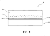
- the structure 1 includes the base component 10 on one side, a resin layer 11 disposed on a faying surface of the base component 10; a metal thin film 12 disposed on a surface of the resin layer 11; the base component 20 on the other side; and a metal thin film 21 disposed on a faying surface of the base component 20.
- the base component 20 is an element to which the base component 10 is bonded.
- the faying surface of the base component 10 is a rough surface.
- a semiconductor substrate such as a silicon (Si) substrate, glass, ceramics, and resin can be used.
- the bonding between base components 10, 20 are not limited to bonding between the same materials such as between metal material components.
- the bonding may be between different materials, for example, between a metal component and a ceramic component, or between an integrated circuit (IC) chip and an Si substrate.
- the shapes of the base components 10, 20 are not limited.
- the base components 10, 20 may have planer shapes or complicated three-dimensional shapes.
- the base component 10 may be, for example, a semiconductor chip that forms a semiconductor.
- the base component 20 may be an Si substrate (silicon substrate) or a semiconductor chip, each of which forms a semiconductor.
- the resin layer 11 is formed to have a predetermined thickness on the faying surface of the base component 10.
- the resin layer 11 is formed by spin coating a liquid resin on the faying surface of the base component 10 and curing the liquid resin.
- the resin layer 11 needs to be selected from resins having characteristics of good bonding compatibility with the metal thin film 12.
- a resin such as a silicone resin, a fluorine resin, a polyimide resin, an acrylic resin, or an epoxy resin may be used.
- the metal thin film 12 having a film thickness of several nm to several hundred nm is formed on the surface of the resin layer 11 by a sputtering film forming method.
- the metal thin film 21 having a film thickness of several nm to 10 nm is formed on the surface of the base component 20 by a similar film forming method.
- a film forming method such as physical vapor deposition (PVD), chemical vapor deposition (CVD), or vacuum deposition, may be used.
- PVD physical vapor deposition
- CVD chemical vapor deposition
- step S1 in FIG. 2 the base component 10 is prepared.
- the faying surface of the base component 10 is rough.
- a polishing process to smooth the rough surface is required when the faying surface is rough, as in this case, no polishing process is performed in the first embodiment and the surface in a rough state is used.
- step S2 a liquid resin 11a is applied on the rough surface of the base component 10.
- the applied liquid resin 11a fills the rough surface and the surface of the liquid resin 11a is smoothed by surface tension of the liquid resin 11a. Specifically, immediately after the application, the surface tension acts on the liquid resin 11a to smooth the surface of the liquid resin 11a. After it is confirmed that the surface of the liquid resin 11a is smoothed, the base component 10 and the liquid resin 11a are heated and the liquid resin 11a is cured to form the resin layer 11.
- step S3 the base component 10 with the resin layer 11 formed thereon is disposed inside a vacuum enclosure.
- the metal thin film 12 is formed by sputtering on the surface of the resin layer 11.
- step S4 the base component 20 is prepared.
- step S5 the base component 20 is disposed inside a vacuum enclosure.
- the metal thin film 21 is formed by sputtering on the surface of the base component 20. Because no smoothing of the surface is required for the surface of the base component 20 that is not a rough surface like that of the base component 10, a liquid resin application, like the one for the base component 10, is not performed.
- step S6 the base components 10, 20 are respectively taken out of the vacuum enclosures.
- the base component 10 is turned over to direct the surface with the metal thin film 12 downwards, and the metal thin film 12 is superposed on the metal thin film 21 of the base component 20.
- a load is applied to the base component 10 so that the metal thin film 12 of the base component 10 and the metal thin film 21 of the base component 20 are tightly attached together.
- the metal thin films 12, 21 are tightly bonded by the atomic diffusion bonding in which the metal thin films 12, 21 are in metal bonding or are intermolecularly bonded at an atomic level.
- the structure 1 is formed by the tight bonding of the metal thin films 12, 21.
- FIGs. 3A , 3B are schematic diagrams in which base components with a rough faying surface are bonded using the atomic diffusion.
- FIG. 3A shows a conventional structure 100
- FIG. 3B shows the structure 1 according to the first embodiment.
- the structure 100 includes a base component 110 that has a rough faying surface; a metal thin film 111 formed on the rough faying surface of the base component 110; a base component 120, and a metal thin film 121 formed on a surface of the base component 120.
- the structure 100 is formed by superposing and bonding the metal thin films 111, 121 using atomic diffusion.
- the surface of the metal thin film 111 formed on this rough surface also has a low smoothness. Accordingly, it becomes difficult to tightly attach and bond the metal thin films 111, 121 using atomic diffusion. This may cause a bonding failure.
- the structure 1 has the resin layer 11 that fills the rough surface of the base component 10 and the surface of the resin layer 11 is a smooth surface, the surface of the metal thin film 12 is also smooth.
- the metal thin films 12, 21 can be tightly attached and bonded together using atomic diffusing.
- the resin layer 11 may be formed between the base component 20 and the metal thin film 21.
- a step similar to step S2 is performed between steps S4 and S5.
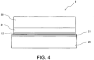
- a faying surface of a base component 30 of a structure 2 is smooth.
- a resin layer 31 has characteristics that differ from those of the resin layer 11.
- Other configurations are identical to those of the structure 1 in the first embodiment.
- elements that are similar to those in FIG. 1 are assigned the same reference numerals and their descriptions are omitted.
- the resin layer 31 of a predetermined thickness is formed on the faying surface (smooth surface) of the base component 30.
- the resin layer 31 is formed by spin coating a liquid resin on the faying surface of the base component 30 and curing the liquid resin.
- the resin layer 31 needs to be selected from resins having characteristics of good bonding compatibility with the metal thin film 12 and elasticity after curing.
- a resin a silicone resin, a fluorine resin, a polyimide resin, acrylic resin, and an epoxy resin may be used.
- step S11 in FIG. 5 the base component 30 is prepared.
- a liquid resin 31a is applied on a faying surface of the base component 30.
- a resin material having elasticity after curing is used as the material for the liquid resin 31a.
- the surface of the applied liquid resin 31a becomes smooth because of surface tension of the liquid resin 31a.
- the base component 30 and the liquid resin 31a are heated, and the liquid resin 31a is cured to form the resin layer 31.
- the resin layer 31 has elasticity after curing.
- step S13 the base component 30 with the resin layer 31 formed thereon is disposed inside a vacuum enclosure.
- the metal thin film 12 is formed by sputtering on the surface of the resin layer 31.
- steps S14, S15 the metal thin film 21 is formed on the base component 20, similarly to as in steps S4, S5.
- the base component 30 is turned over to direct the surface with the metal thin film 12 downwards, and the metal thin film 12 is superposed on the metal thin film 21 of the base component 20.
- a load is applied to the base component 30 so that the metal thin film 12 of the base component 30 and the metal thin film 21 of the base component 20 are tightly attached together.
- the metal thin films 12, 21 are tightly bonded by the atomic diffusion in which the metal thin films 12, 21 are in metal bonding, or are bonded at an atomic or intermolecular level.
- the structure 2 is formed by the tight bonding of the metal thin films 12, 21.
- FIGs. 6A , 6B are schematic diagrams which are used to describe cases where a contaminant D has entered between the metal thin films.
- FIG. 6A shows a conventional structure 200
- FIG. 6B shows the structure 2 according to the second embodiment.
- the conventional structure 200 includes a base component 210, a metal thin film 211 formed on a surface of the base component 210, a base component 220, and a metal thin film 221 formed on a surface of the base component 220.
- the structure 200 is formed by superposing and bonding the metal thin films 211, 221 using atomic diffusion.
- the resin layer 31 elastically deforms in accordance with the shape of the contaminant D when the metal thin films 12, 21 are superposed together with the contaminant D having entered there between. With the contaminant D being enclosed, the metal thin films 12, 21 are tightly attached together. Specifically, the metal thin films 12, 21 are tightly attached together except for the area with the contaminant D.
- the structure 2 can be obtained even when the contaminant D has entered, because the area excluding the contaminant D has a sufficient overlapping area to enable bonding of the metal thin films 12, 21 using the atomic diffusion.
- the metal thin films 12, 21 can be bonded using the atomic diffusion because the resin layer 31 can elastically deform to enable tight attachment of the metal thin films 12, 21.
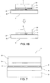
- a resin layer 22 is formed on the other base component 20. Specifically, the resin layer 22 is formed on a faying surface of the base component 20. As a material for the resin layer 22, a material that has elasticity after curing is used, similarly as for the resin layer 31.
- the resin layers 31, 22 elastically deform in accordance with the shape of the contaminant D when the contaminant D has entered between the metal thin films 12, 21.
- the metal thin films 12, 21 can be bonded using the atomic diffusion because the metal thin films 12, 21 are tightly attached together even with the contaminant D sandwiched therebetween.
- the elastically deformable amount is increased by the resin layers 31, 22, it becomes possible to accommodate a larger contaminant D and improve correspondence between the surfaces of the metal thin films 12, 21, enhancing the tight attachment between the metal thin films 12, 21.
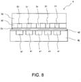
- the structure is a semiconductor assembly 4.
- the semiconductor assembly 4 includes a substrate 40, a chip component 50, a resin layer 52 which is provided between electrodes 51 of the chip component 50, and metal thin films 42, 53 that bond the substrate 40 and the chip component 50 together.
- the chip component 50 is, for example, a semiconductor chip that forms a semiconductor.
- the substrate 40 is a silicone (Si) substrate. Multiple electrodes 41 are embedded in the substrate 40. Multiple electrodes 51 are disposed on the lower surface of the chip component 50 and protrude from the lower surface for a predetermined length. The multiple electrodes 51 are arranged to correspond to the respective electrodes 41 disposed on the substrate 40.
- a liquid resin similar to the liquid resin 11a in the first embodiment is applied between the electrodes 51 such that the distal surfaces of the electrodes 51 and the surface of the liquid resin are in the same plane.
- the surface of the liquid resin becomes smooth as a result of surface tension of the liquid resin. This smooth surface is in the same plane as the distal surfaces of the electrodes 51.
- the resin layer 52 is formed by curing the liquid resin in this state.
- the metal thin film 53 similar to the metal thin film 12 in the first embodiment is formed on the distal surfaces of the electrodes 51 of the chip component 50 and the surface of the resin layer 52.
- a metal thin film 42 similar to the metal thin film 12 in the first embodiment is formed on the surface of the substrate 40.
- the chip component 50 and the substrate 40 are bonded and the semiconductor assembly 4 is formed by placing the electrodes 51 of the chip component 50 and the electrodes 41 of the substrate 40 to oppose each other, and bonding the metal thin films 42, 53 using the atomic diffusion.
- the area where the metal thin film 53 is formed is enlarged by forming the resin layer 52 between the electrodes 51 of the chip component 50 so that the chip component 50 and the substrate 40 can be more tightly bonded using the atomic diffusion.
- a structure may be formed by stacking multiple semiconductor chips (intermediate chip components, and outermost chip components sandwiching the intermediate chip components), and bonding the chip components using atomic diffusion.
- Each intermediate chip component may be formed by applying a liquid resin to both the front and back surfaces of a semiconductor chip, curing the liquid resin to form resin layers on both surfaces, and forming metal thin films on the resin layers.
- Each of the outermost chip components may be formed by applying a liquid resin to a front or back surface of a semiconductor chip and curing the liquid resin to form a resin layer on one of the surfaces, and forming a metal thin layer thereon.
Landscapes
- Engineering & Computer Science (AREA)
- Mechanical Engineering (AREA)
- Pressure Welding/Diffusion-Bonding (AREA)
- Manufacturing & Machinery (AREA)
- Die Bonding (AREA)
Abstract
Description
- The present disclosure relates to a structure manufacturing method and a manufactured structure, in particular to a structure manufacturing method using an atomic diffusion bonding method, and a structure manufactured by the atomic diffusion bonding method.
- A structure may be manufactured by bonding multiple elements. For example, a semiconductor assembly may be manufactured by bonding (laminating) semiconductor devices and substrates.
Patent Literature 1 discloses a bonding method by forming a resin layer over a surface of a substrate to cover electrodes on the surface of the substrate and bonding semiconductor devices to the electrodes on the substrate while melting the resin layer. This manufacturing method can reduce contaminants entering between the electrodes and the semiconductor devices on the substrate. - Recently, besides the above described bonding method, an atomic diffusion bonding method for elements are known. In the atomic diffusion bonding method, a metal thin film is formed on each of a pair of facing surfaces of elements. The elements are bonded by tightly attaching the metal thin films together to cause atomic diffusion. Because the atomic diffusion bonding method can be performed at room temperature, the bonding is possible without applying heat to the elements, and is applicable to elements of different materials having different coefficients of thermal expansion. Further, because the bonding is achieved at an atomic level, no adhesive agent is required. The atomic diffusion bonding method is excellent in bonding strength, reliability, and durability.
- Patent Literature 1:
JP 2013-168503A - In the atomic diffusion bonding method, because elements are bonded via metal thin films formed on surfaces of the elements, it is necessary to tightly attach the metal thin films together. Accordingly, thin film forming surfaces on which the metal thin films are to be formed need to be smooth.
- When the thin film forming surfaces of the elements are not smooth, for example, when the thin film forming surfaces are rough, a process such as a polishing process to polish the surfaces (thin film forming surfaces) of the elements is necessary to make the thin film forming surfaces of the elements smooth. This polishing process is complex, increasing the cost. When contaminants exist between the metal thin films of the elements to be bonded, tight attachment between the metal thin films of the elements becomes unlikely, making bonding using the atomic diffusion difficult.
- An object of the present disclosure is to enable atomic diffusion bonding even when thin film forming surfaces of elements are not smooth, or even when a contaminant exists between the metal thin films of the elements.
- A manufacturing method of a structure according to the present disclosure is a manufacturing method of a structure in which multiple elements are bonded using atomic diffusion. The method includes applying a liquid resin to a surface of at least one of the elements, and smoothing a surface of the liquid resin using surface tension of the applied liquid resin. The method also includes forming a resin layer by curing the liquid resin, forming a metal thin film on a surface of the resin layer, and forming another metal thin film on a surface of another element. The method further includes tightly attaching and bonding the metal thin film of the at least one element and the metal thin film of the other element.
- Another manufacturing method of a structure according to the present disclosure is a manufacturing method of a structure in which multiple elements are bonded using atomic diffusion, and the method includes applying a liquid resin to surfaces of the multiple elements and smoothing surfaces of the liquid resin using surface tension of the applied liquid resin. The method also includes forming resin layers by curing the liquid resin, forming a metal thin film on a surface of each of the resin layers, and tightly attaching and bonding the metal thin films of the multiple elements to one another.
- In the manufacturing method of the structure according to the present disclosure, the resin layers may have elasticity, and the multiple elements may be semiconductors.
- In the manufacturing method of the structure according to the present disclosure, at least one of the semiconductors may include multiple electrodes that protrude from a surface of the at least one semiconductor for a predetermined length, and the liquid resin may be applied between the electrodes. The surface of the liquid resin may be smoothed by surface tension of the liquid resin such that distal end surfaces of the multiple electrodes and the surface of the liquid resin are in the same plane.
- In the manufacturing method of the structure according to the present disclosure, the elements may be semiconductor chips that form semiconductors. The liquid resin may be applied to a front surface and/or a back surface of each of the semiconductor chips. The applied liquid resin may be smoothed to have a surface roughness lower than that of the other element.
- A structure according to the present disclosure is a structure in which metal thin films are formed on respective surfaces of multiple elements such that the multiple elements are bonded via the metal thin films. The structure further comprises a resin layer disposed between at least one of the multiple elements and the metal thin film, and a surface of the resin layer is smoothed. The resin layer has elasticity.
- In the structure according to the present disclosure, the at least one element may be a semiconductor chip, and the resin layer may have a surface roughness lower than that of the other element to be bonded.
- According to the present disclosure, even when a thin film faying surface of an element is not smooth, because a smooth thin film faying surface can be formed in a simple method, bonding using atomic diffusion is possible. Further, even when a contaminant exists between metal thin films of the elements, bonding using atomic diffusion is possible.
-
-
FIG. 1 is a schematic configuration diagram of a structure according to a first embodiment; -
FIG. 2 is a manufacturing process diagram of the structure according to the first embodiment; -
FIG. 3A is a schematic diagram showing a conventional structure with a rough substrate surface; -
FIG. 3B is a schematic diagram of the structure according to the first embodiment with a rough substrate surface; -
FIG. 4 is a schematic diagram of a structure according to a second embodiment; -
FIG. 5 is a manufacturing process diagram of the structure according to the second embodiment; -
FIG. 6A is a schematic diagram showing a conventional structure when a contaminant has entered between metal thin films; -
FIG.6B is a schematic diagram of the structure according to the second embodiment when a contaminant has entered between the metal thin films; -
FIG. 7 is a schematic configuration diagram of a variation of the structure according to the second embodiment; and -
FIG. 8 is a schematic configuration diagram of a structure according to a third embodiment. - Initially, a first embodiment will be described by reference to
FIGs. 1 to 3 . As shown inFIG. 1 , astructure 1 according to the first embodiment is formed by bonding a pair of elements,base components structure 1 including a single pair ofbase components base components - The
structure 1 includes thebase component 10 on one side, aresin layer 11 disposed on a faying surface of thebase component 10; a metalthin film 12 disposed on a surface of theresin layer 11; thebase component 20 on the other side; and a metalthin film 21 disposed on a faying surface of thebase component 20. Thebase component 20 is an element to which thebase component 10 is bonded. - The faying surface of the
base component 10 is a rough surface. As a material for thebase components base components base components base components base component 10 may be, for example, a semiconductor chip that forms a semiconductor. Thebase component 20 may be an Si substrate (silicon substrate) or a semiconductor chip, each of which forms a semiconductor. - The
resin layer 11 is formed to have a predetermined thickness on the faying surface of thebase component 10. Theresin layer 11 is formed by spin coating a liquid resin on the faying surface of thebase component 10 and curing the liquid resin. Theresin layer 11 needs to be selected from resins having characteristics of good bonding compatibility with the metalthin film 12. For example, a resin, such as a silicone resin, a fluorine resin, a polyimide resin, an acrylic resin, or an epoxy resin may be used. - The metal
thin film 12 having a film thickness of several nm to several hundred nm is formed on the surface of theresin layer 11 by a sputtering film forming method. The metalthin film 21 having a film thickness of several nm to 10 nm is formed on the surface of thebase component 20 by a similar film forming method. Besides the sputtering, a film forming method, such as physical vapor deposition (PVD), chemical vapor deposition (CVD), or vacuum deposition, may be used. As a material for the metalthin films - Next, a manufacturing method of the
structure 1 will be described by reference toFIG. 2 . First, in step S1 inFIG. 2 , thebase component 10 is prepared. The faying surface of thebase component 10 is rough. Although a polishing process to smooth the rough surface is required when the faying surface is rough, as in this case, no polishing process is performed in the first embodiment and the surface in a rough state is used. - In step S2, a
liquid resin 11a is applied on the rough surface of thebase component 10. The appliedliquid resin 11a fills the rough surface and the surface of theliquid resin 11a is smoothed by surface tension of theliquid resin 11a. Specifically, immediately after the application, the surface tension acts on theliquid resin 11a to smooth the surface of theliquid resin 11a. After it is confirmed that the surface of theliquid resin 11a is smoothed, thebase component 10 and theliquid resin 11a are heated and theliquid resin 11a is cured to form theresin layer 11. - In step S3, the
base component 10 with theresin layer 11 formed thereon is disposed inside a vacuum enclosure. The metalthin film 12 is formed by sputtering on the surface of theresin layer 11. - Meanwhile, in step S4, the
base component 20 is prepared. In step S5, thebase component 20 is disposed inside a vacuum enclosure. The metalthin film 21 is formed by sputtering on the surface of thebase component 20. Because no smoothing of the surface is required for the surface of thebase component 20 that is not a rough surface like that of thebase component 10, a liquid resin application, like the one for thebase component 10, is not performed. - In step S6, the
base components base component 10 is turned over to direct the surface with the metalthin film 12 downwards, and the metalthin film 12 is superposed on the metalthin film 21 of thebase component 20. In such a superposed state, a load is applied to thebase component 10 so that the metalthin film 12 of thebase component 10 and the metalthin film 21 of thebase component 20 are tightly attached together. This tight attachment bonds the metalthin films thin films thin films structure 1 is formed by the tight bonding of the metalthin films - In comparing a surface Ra (the arithmetic average of the roughness) of the
base component 10 with a surface Ra of theresin layer 11, the surface Ra of theresin layer 11 is lower than the surface Ra of thebase component 10. In other words, because the surface of theresin layer 11 is smoothed, the surface Ra is low, whereas because the surface is rough, the surface Ra of thebase component 10 is high. This results in a relationship of the surface Ra of theresin layer 11 < the surface Ra of thebase component 10. Smoothing of theresin layer 11 makes the surface Ra of theresin layer 11 lower than the surface Ra of thebase component 20 that has a smooth surface and does not require the smoothing of the surface. - With reference to
FIGs. 3A ,3B , advantages of thestructure 1 will be described.FIGs. 3A ,3B are schematic diagrams in which base components with a rough faying surface are bonded using the atomic diffusion.FIG. 3A shows aconventional structure 100, whereasFIG. 3B shows thestructure 1 according to the first embodiment. - With reference to
FIG. 3A , the configuration of theconventional structure 100 will be briefly described. Thestructure 100 includes abase component 110 that has a rough faying surface; a metalthin film 111 formed on the rough faying surface of thebase component 110; abase component 120, and a metalthin film 121 formed on a surface of thebase component 120. Thestructure 100 is formed by superposing and bonding the metalthin films - In the
structure 100, because of the low smoothness of the rough surface of thebase component 110, the surface of the metalthin film 111 formed on this rough surface also has a low smoothness. Accordingly, it becomes difficult to tightly attach and bond the metalthin films - In contrast, as shown in
FIG. 3B , because thestructure 1 has theresin layer 11 that fills the rough surface of thebase component 10 and the surface of theresin layer 11 is a smooth surface, the surface of the metalthin film 12 is also smooth. Thus, the metalthin films - As described above, because no polishing process is required to smooth the rough surface of the
base component 10, cost can be reduced by omitting polishing procedures. Further, because the atomic diffusion bonding is possible even with a rough surface of thebase component 10, the applicable range of the bondable materials by atomic diffusion can be extended. - When the surface of the
base component 20 on which the metalthin film 21 is to be formed is rough, theresin layer 11 may be formed between thebase component 20 and the metalthin film 21. In this case, inFIG. 2 , a step similar to step S2 is performed between steps S4 and S5. - Next, a second embodiment will be described by reference to
FIGs. 4 to 6 . In the second embodiment, a faying surface of abase component 30 of astructure 2 is smooth. Aresin layer 31 has characteristics that differ from those of theresin layer 11. Other configurations are identical to those of thestructure 1 in the first embodiment. InFIG. 4 , elements that are similar to those inFIG. 1 are assigned the same reference numerals and their descriptions are omitted. - The
resin layer 31 of a predetermined thickness is formed on the faying surface (smooth surface) of thebase component 30. Theresin layer 31 is formed by spin coating a liquid resin on the faying surface of thebase component 30 and curing the liquid resin. Theresin layer 31 needs to be selected from resins having characteristics of good bonding compatibility with the metalthin film 12 and elasticity after curing. As an example of such a resin, a silicone resin, a fluorine resin, a polyimide resin, acrylic resin, and an epoxy resin may be used. - With reference to
FIG. 5 , manufacturing of thestructure 2 will be described. In step S11 inFIG. 5 , thebase component 30 is prepared. - In step S12, a
liquid resin 31a is applied on a faying surface of thebase component 30. As the material for theliquid resin 31a, a resin material having elasticity after curing is used. The surface of the appliedliquid resin 31a becomes smooth because of surface tension of theliquid resin 31a. After the surface of theliquid resin 31a has been smoothed, thebase component 30 and theliquid resin 31a are heated, and theliquid resin 31a is cured to form theresin layer 31. Theresin layer 31 has elasticity after curing. - In step S13, the
base component 30 with theresin layer 31 formed thereon is disposed inside a vacuum enclosure. The metalthin film 12 is formed by sputtering on the surface of theresin layer 31. - In steps S14, S15, the metal
thin film 21 is formed on thebase component 20, similarly to as in steps S4, S5. Subsequently, in S16, thebase component 30 is turned over to direct the surface with the metalthin film 12 downwards, and the metalthin film 12 is superposed on the metalthin film 21 of thebase component 20. In such a superposed state, a load is applied to thebase component 30 so that the metalthin film 12 of thebase component 30 and the metalthin film 21 of thebase component 20 are tightly attached together. This tight attachment bonds the metalthin films thin films thin films structure 2 is formed by the tight bonding of the metalthin films - Advantages of the
structure 2 will be described with reference toFIGs. 6A ,6B .FIGs 6A ,6B are schematic diagrams which are used to describe cases where a contaminant D has entered between the metal thin films.FIG. 6A shows aconventional structure 200, whileFIG. 6B shows thestructure 2 according to the second embodiment. - In
FIG. 6A , theconventional structure 200 includes abase component 210, a metalthin film 211 formed on a surface of thebase component 210, abase component 220, and a metalthin film 221 formed on a surface of thebase component 220. Thestructure 200 is formed by superposing and bonding the metalthin films - In the
structure 200, when the contaminant D has entered between the metalthin films thin films thin films thin films - In contrast, as shown in
FIG. 6B , in thestructure 2 according to the second embodiment, theresin layer 31 elastically deforms in accordance with the shape of the contaminant D when the metalthin films thin films thin films - The
structure 2 can be obtained even when the contaminant D has entered, because the area excluding the contaminant D has a sufficient overlapping area to enable bonding of the metalthin films - Further, even when the surfaces of the metal
thin films thin films resin layer 31 can elastically deform to enable tight attachment of the metalthin films - Next, variations of the second embodiment will described by reference to
FIG. 7 . As shown inFIG. 7 , in astructure 3 that shows a variation of the second embodiment, aresin layer 22 is formed on theother base component 20. Specifically, theresin layer 22 is formed on a faying surface of thebase component 20. As a material for theresin layer 22, a material that has elasticity after curing is used, similarly as for theresin layer 31. - As described above, by forming the resin layers 31, 22 on both of the
base components thin films thin films thin films - Further, because the elastically deformable amount is increased by the resin layers 31, 22, it becomes possible to accommodate a larger contaminant D and improve correspondence between the surfaces of the metal
thin films thin films - Next, a third embodiment will be described with reference to
FIG. 8 . In the third embodiment, the structure is asemiconductor assembly 4. As shown inFIG. 8 , thesemiconductor assembly 4 includes asubstrate 40, achip component 50, aresin layer 52 which is provided betweenelectrodes 51 of thechip component 50, and metalthin films substrate 40 and thechip component 50 together. Thechip component 50 is, for example, a semiconductor chip that forms a semiconductor. - The
substrate 40 is a silicone (Si) substrate.Multiple electrodes 41 are embedded in thesubstrate 40.Multiple electrodes 51 are disposed on the lower surface of thechip component 50 and protrude from the lower surface for a predetermined length. Themultiple electrodes 51 are arranged to correspond to therespective electrodes 41 disposed on thesubstrate 40. - A liquid resin similar to the
liquid resin 11a in the first embodiment is applied between theelectrodes 51 such that the distal surfaces of theelectrodes 51 and the surface of the liquid resin are in the same plane. By applying the liquid resin between theelectrodes 51 of thechip component 50, the surface of the liquid resin becomes smooth as a result of surface tension of the liquid resin. This smooth surface is in the same plane as the distal surfaces of theelectrodes 51. Theresin layer 52 is formed by curing the liquid resin in this state. - The metal
thin film 53 similar to the metalthin film 12 in the first embodiment is formed on the distal surfaces of theelectrodes 51 of thechip component 50 and the surface of theresin layer 52. Similarly, a metalthin film 42 similar to the metalthin film 12 in the first embodiment is formed on the surface of thesubstrate 40. Thechip component 50 and thesubstrate 40 are bonded and thesemiconductor assembly 4 is formed by placing theelectrodes 51 of thechip component 50 and theelectrodes 41 of thesubstrate 40 to oppose each other, and bonding the metalthin films - As described above, the area where the metal
thin film 53 is formed is enlarged by forming theresin layer 52 between theelectrodes 51 of thechip component 50 so that thechip component 50 and thesubstrate 40 can be more tightly bonded using the atomic diffusion. - Although two base components are bonded using the atomic diffusion in the above respective embodiments, the present disclosure is not limited to these embodiments. For example, a structure may be formed by stacking multiple semiconductor chips (intermediate chip components, and outermost chip components sandwiching the intermediate chip components), and bonding the chip components using atomic diffusion. Each intermediate chip component may be formed by applying a liquid resin to both the front and back surfaces of a semiconductor chip, curing the liquid resin to form resin layers on both surfaces, and forming metal thin films on the resin layers. Each of the outermost chip components may be formed by applying a liquid resin to a front or back surface of a semiconductor chip and curing the liquid resin to form a resin layer on one of the surfaces, and forming a metal thin layer thereon.
-
- 1, 2, 3 structure,
- 4 semiconductor assembly
- 10, 20, 30, 40 base component
- 11, 22, 31, 52 resin layer
- 11a, 31a liquid resin
- 12, 21, 42, 53 metal thin film
- 41, 51 electrode
- 50 chip component
Claims (21)
- A manufacturing method of a structure in which a plurality of elements are bonded, the manufacturing method comprising:applying a liquid resin to a surface of at least one of the plurality of elements;smoothing a surface of the liquid resin by surface tension of the applied liquid resin;forming a resin layer by curing the liquid resin;forming a metal thin film on a surface of the resin layer;forming another metal thin film on a surface of another element; andtightly attaching and bonding the metal thin film of the at least one element and the metal thin film of the other element.
- The manufacturing method of the structure according to claim 1, wherein
the resin layer has elasticity. - The manufacturing method of the structure according to claim 1, wherein
the plurality of elements are semiconductors. - The manufacturing method of the structure according to claim 2, wherein
the plurality of elements are semiconductors. - The manufacturing method of the structure according to claim 3, whereinat least one of the semiconductors comprises a plurality of electrodes protruding from a surface of the at least one semiconductor for a predetermined length; andthe liquid resin is applied between the plurality of electrodes, and the surface of the liquid resin is smoothed by surface tension of the liquid resin such that distal end surfaces of the plurality of electrodes and the surface of the liquid resin are in the same plane.
- The manufacturing method of the structure according to claim 4, whereinat least one of the semiconductors comprises a plurality of electrodes protruding from a surface of the at least one semiconductor for a predetermined length; andthe liquid resin is applied between the plurality of electrodes, and the surface of the liquid resin is smoothed by surface tension of the liquid resin such that distal end surfaces of the plurality of electrodes and the surface of the liquid resin are in the same plane.
- The manufacturing method of the structure according to any one of claims 1 to 6, wherein
the metal thin film of the at least one element is bonded to the metal thin film of the other element using atomic diffusion. - The manufacturing method of the structure according to claim 3, whereinthe plurality of elements are semiconductor chips that form semiconductors,the liquid resin is applied to a front surface and/or a back surface of each of the semiconductor chips, andthe applied liquid resin is smoothed to have a surface roughness lower than that of the other element.
- The manufacturing method of the structure according to claim 4, whereinthe plurality of elements are semiconductor chips that form semiconductors,the liquid resin is applied to a front surface and/or a back surface of each of the semiconductor chips, andthe applied liquid resin is smoothed to have a surface roughness lower than that of the other element.
- A manufacturing method of a structure in which a plurality of elements are bonded, the manufacturing method comprising:applying a liquid resin to surfaces of the plurality of elements;smoothing surfaces of the liquid resin using surface tension of the applied liquid resin;forming resin layers by curing the liquid resin;forming a metal thin film on a surface of each of the resin layers; andtightly attaching and bonding the metal thin films of the plurality of elements to one another.
- The manufacturing method of the structure according to claim 10, wherein
the resin layers have elasticity. - The manufacturing method of the structure according to claim 10, wherein
the plurality of elements are semiconductors. - The manufacturing method of the structure according to claim 11, wherein
the plurality of elements are semiconductors. - The manufacturing method of the structure according to claim 12, whereinat least one of the semiconductors comprises a plurality of electrodes protruding from a surface of the at least one semiconductor for a predetermined length; andthe liquid resin is applied between the plurality of electrodes, and the surface of the liquid resin is smoothed by surface tension of the liquid resin such that distal end surfaces of the plurality of electrodes and the surface of the liquid resin are in the same plane.
- The manufacturing method of the structure according to claim 13, whereinat least one of the semiconductors comprises a plurality of electrodes protruding from a surface of the at least one semiconductor for a predetermined length; andthe liquid resin is applied between the plurality of electrodes, and the surface of the liquid resin is smoothed by surface tension of the liquid resin such that distal end surfaces of the plurality of electrodes and the surface of the liquid resin are in the same plane.
- The manufacturing method of the structure according to any one of claims 10 to 15, wherein
the metal thin film of at least one of the plurality of elements is bonded to the metal thin film of another element using atomic diffusion. - The manufacturing method of the structure according to claim 12, whereinthe plurality of elements are semiconductor chips that form semiconductors,the liquid resin is applied to a front surface and/or a back surface of each of the semiconductor chips, andthe applied liquid resin is smoothed to have a surface roughness lower than that of another element.
- The manufacturing method of the structure according to claim 13, whereinthe plurality of elements are semiconductor chips that form semiconductors,the liquid resin is applied to a front surface and/or a back surface of each of the semiconductor chips, andthe applied liquid resin is smoothed to have a surface roughness lower than that of another element.
- A structure in which metal thin films are formed on respective surfaces of a plurality of elements such that the plurality of elements are bonded via the metal thin films,
the structure comprising a resin layer disposed between at least one of the plurality of elements and the metal thin film, and a surface of the resin layer is smoothed. - The structure according to claim 19, wherein
the resin layer has elasticity. - The structure according to claim 19, whereinthe at least one element is a semiconductor chip, andthe resin layer has a surface roughness lower than that of the other element to be bonded.
Applications Claiming Priority (2)
| Application Number | Priority Date | Filing Date | Title |
|---|---|---|---|
| JP2017103175 | 2017-05-25 | ||
| PCT/JP2018/019972 WO2018216763A1 (en) | 2017-05-25 | 2018-05-24 | Method for producing structure, and structure |
Publications (2)
| Publication Number | Publication Date |
|---|---|
| EP3633713A1 true EP3633713A1 (en) | 2020-04-08 |
| EP3633713A4 EP3633713A4 (en) | 2021-03-03 |
Family
ID=64395567
Family Applications (1)
| Application Number | Title | Priority Date | Filing Date |
|---|---|---|---|
| EP18806139.4A Pending EP3633713A4 (en) | 2017-05-25 | 2018-05-24 | STRUCTURE AND STRUCTURE PRODUCTION PROCESS |
Country Status (7)
| Country | Link |
|---|---|
| US (1) | US11569192B2 (en) |
| EP (1) | EP3633713A4 (en) |
| JP (1) | JP6807585B2 (en) |
| KR (2) | KR20190142382A (en) |
| CN (1) | CN110651359A (en) |
| TW (1) | TWI691407B (en) |
| WO (1) | WO2018216763A1 (en) |
Families Citing this family (6)
| Publication number | Priority date | Publication date | Assignee | Title |
|---|---|---|---|---|
| JP7363027B2 (en) * | 2018-12-20 | 2023-10-18 | 三菱マテリアル株式会社 | Method for manufacturing a bonded body and method for manufacturing an insulated circuit board |
| US12023892B2 (en) | 2019-01-07 | 2024-07-02 | Sony Group Corporation | Structure body, structure body manufacturing method, and electronic apparatus |
| JP2021146359A (en) * | 2020-03-18 | 2021-09-27 | 三菱マテリアル株式会社 | Joined body and method for manufacturing joined body |
| CN115428127B (en) * | 2020-04-13 | 2025-02-18 | 三菱电机株式会社 | Method for manufacturing semiconductor element |
| WO2022172349A1 (en) * | 2021-02-10 | 2022-08-18 | キヤノンアネルバ株式会社 | Chemical bonding method and packaged electronic component |
| US20230411325A1 (en) * | 2022-06-15 | 2023-12-21 | Xilinx, Inc. | Chip package integration with hybrid bonding |
Family Cites Families (17)
| Publication number | Priority date | Publication date | Assignee | Title |
|---|---|---|---|---|
| US4646266A (en) * | 1984-09-28 | 1987-02-24 | Energy Conversion Devices, Inc. | Programmable semiconductor structures and methods for using the same |
| JP2821830B2 (en) | 1992-05-14 | 1998-11-05 | セイコーインスツルメンツ株式会社 | Semiconductor thin film device and its application device and method of manufacturing semiconductor thin film device |
| JP3297254B2 (en) * | 1995-07-05 | 2002-07-02 | 株式会社東芝 | Semiconductor package and manufacturing method thereof |
| US6333206B1 (en) * | 1996-12-24 | 2001-12-25 | Nitto Denko Corporation | Process for the production of semiconductor device |
| US20020123228A1 (en) * | 2001-03-02 | 2002-09-05 | Smoak Richard C. | Method to improve the reliability of gold to aluminum wire bonds with small pad openings |
| US6962835B2 (en) * | 2003-02-07 | 2005-11-08 | Ziptronix, Inc. | Method for room temperature metal direct bonding |
| TW200507218A (en) * | 2003-03-31 | 2005-02-16 | North Corp | Layout circuit substrate, manufacturing method of layout circuit substrate, and circuit module |
| JP5070557B2 (en) * | 2007-02-27 | 2012-11-14 | 武仁 島津 | Room temperature bonding method |
| JP4462332B2 (en) * | 2007-11-05 | 2010-05-12 | セイコーエプソン株式会社 | Electronic components |
| WO2010007715A1 (en) | 2008-07-17 | 2010-01-21 | 株式会社 村田製作所 | Manufacturing method of a parts installation module |
| JP5826532B2 (en) * | 2010-07-15 | 2015-12-02 | 新光電気工業株式会社 | Semiconductor device and manufacturing method thereof |
| JP2012238699A (en) * | 2011-05-11 | 2012-12-06 | Hitachi Chem Co Ltd | Semiconductor device manufacturing method, semiconductor wafer with semiconductor element manufacturing method and semiconductor wafer with adhesive layer manufacturing method |
| US20120305298A1 (en) | 2011-05-31 | 2012-12-06 | Industrial Technology Research Institute | Bump with nanolaminated structure, package structure of the same, and method of preparing the same |
| JP2013168503A (en) | 2012-02-15 | 2013-08-29 | Sumitomo Bakelite Co Ltd | Method of manufacturing semiconductor device |
| FR2987626B1 (en) * | 2012-03-05 | 2015-04-03 | Commissariat Energie Atomique | DIRECT COLLECTION METHOD USING COMPRESSIBLE POROUS LAYER |
| JP6147176B2 (en) * | 2013-12-02 | 2017-06-14 | 三菱電機株式会社 | Method for bonding semiconductor element to substrate |
| JP6668608B2 (en) * | 2015-04-27 | 2020-03-18 | 日亜化学工業株式会社 | Light emitting device manufacturing method |
-
2018
- 2018-05-24 JP JP2019520304A patent/JP6807585B2/en active Active
- 2018-05-24 TW TW107117815A patent/TWI691407B/en active
- 2018-05-24 EP EP18806139.4A patent/EP3633713A4/en active Pending
- 2018-05-24 KR KR1020197034973A patent/KR20190142382A/en not_active Ceased
- 2018-05-24 CN CN201880033360.8A patent/CN110651359A/en active Pending
- 2018-05-24 US US16/615,816 patent/US11569192B2/en active Active
- 2018-05-24 WO PCT/JP2018/019972 patent/WO2018216763A1/en not_active Ceased
- 2018-05-24 KR KR1020227001488A patent/KR102404406B1/en active Active
Also Published As
| Publication number | Publication date |
|---|---|
| JP6807585B2 (en) | 2021-01-06 |
| TW201900403A (en) | 2019-01-01 |
| KR20190142382A (en) | 2019-12-26 |
| KR102404406B1 (en) | 2022-06-03 |
| EP3633713A4 (en) | 2021-03-03 |
| WO2018216763A1 (en) | 2018-11-29 |
| JPWO2018216763A1 (en) | 2020-05-21 |
| TWI691407B (en) | 2020-04-21 |
| US11569192B2 (en) | 2023-01-31 |
| CN110651359A (en) | 2020-01-03 |
| KR20220011807A (en) | 2022-01-28 |
| US20200083190A1 (en) | 2020-03-12 |
Similar Documents
| Publication | Publication Date | Title |
|---|---|---|
| US11569192B2 (en) | Method for producing structure, and structure | |
| US10090351B2 (en) | Semiconductor device having gaps within the conductive parts | |
| EP0332402B1 (en) | Connection construction and method of manufacturing the same | |
| US5177032A (en) | Method for attaching a semiconductor die to a leadframe using a thermoplastic covered carrier tape | |
| US20100308455A1 (en) | Method for Manufacturing Hetero-Bonded Wafer | |
| US5693574A (en) | Process for the laminar joining of silicon semiconductor slices | |
| TW201419973A (en) | Method and flexible device for providing flexible structure | |
| TW200727446A (en) | Stack type semiconductor device manufacturing method and stack type electronic component manufacturing method | |
| US7811862B2 (en) | Thermally enhanced electronic package | |
| US20070020908A1 (en) | Multilayer structure having a warpage-compensating layer | |
| JP2835145B2 (en) | Electronic equipment | |
| US20070159803A1 (en) | MEMS device seal using liquid crystal polymer | |
| JP2010040662A (en) | Method of manufacturing semiconductor device | |
| US20090096074A1 (en) | Semiconductor device | |
| JP3199747B2 (en) | Chip module | |
| JPH113909A (en) | Flip chip member, sheet-like sealing material, semiconductor device, and method of manufacturing the same | |
| JP2004533119A (en) | Integrated circuit with energy absorbing structure | |
| JP7596650B2 (en) | Superconducting device and manufacturing method thereof | |
| JP2529799B2 (en) | Method for joining silicon semiconductor devices | |
| JP7600546B2 (en) | Superconducting device and manufacturing method thereof | |
| US10062622B2 (en) | Electrolytic seal | |
| US11251137B2 (en) | Semiconductor device | |
| JP2019114607A (en) | Semiconductor device and method of manufacturing the same | |
| WO2025084109A1 (en) | Semiconductor device and method for manufacturing semiconductor device | |
| JP2006210802A (en) | Semiconductor device |
Legal Events
| Date | Code | Title | Description |
|---|---|---|---|
| STAA | Information on the status of an ep patent application or granted ep patent |
Free format text: STATUS: THE INTERNATIONAL PUBLICATION HAS BEEN MADE |
|
| PUAI | Public reference made under article 153(3) epc to a published international application that has entered the european phase |
Free format text: ORIGINAL CODE: 0009012 |
|
| STAA | Information on the status of an ep patent application or granted ep patent |
Free format text: STATUS: REQUEST FOR EXAMINATION WAS MADE |
|
| 17P | Request for examination filed |
Effective date: 20191212 |
|
| AK | Designated contracting states |
Kind code of ref document: A1 Designated state(s): AL AT BE BG CH CY CZ DE DK EE ES FI FR GB GR HR HU IE IS IT LI LT LU LV MC MK MT NL NO PL PT RO RS SE SI SK SM TR |
|
| AX | Request for extension of the european patent |
Extension state: BA ME |
|
| DAV | Request for validation of the european patent (deleted) | ||
| DAX | Request for extension of the european patent (deleted) | ||
| REG | Reference to a national code |
Ref country code: DE Ref legal event code: R079 Free format text: PREVIOUS MAIN CLASS: H01L0021520000 Ipc: H01L0021580000 |
|
| A4 | Supplementary search report drawn up and despatched |
Effective date: 20210203 |
|
| RIC1 | Information provided on ipc code assigned before grant |
Ipc: H01L 25/065 20060101ALI20210128BHEP Ipc: H01L 21/98 20060101ALI20210128BHEP Ipc: H01L 21/58 20060101AFI20210128BHEP Ipc: B23K 20/233 20060101ALI20210128BHEP Ipc: B23K 20/02 20060101ALI20210128BHEP Ipc: B32B 15/04 20060101ALI20210128BHEP Ipc: B23K 20/24 20060101ALI20210128BHEP |
|
| STAA | Information on the status of an ep patent application or granted ep patent |
Free format text: STATUS: EXAMINATION IS IN PROGRESS |
|
| 17Q | First examination report despatched |
Effective date: 20251016 |