EP3631891B1 - Waveguide device with switchable polarization configurations - Google Patents
Waveguide device with switchable polarization configurations Download PDFInfo
- Publication number
- EP3631891B1 EP3631891B1 EP18719378.4A EP18719378A EP3631891B1 EP 3631891 B1 EP3631891 B1 EP 3631891B1 EP 18719378 A EP18719378 A EP 18719378A EP 3631891 B1 EP3631891 B1 EP 3631891B1
- Authority
- EP
- European Patent Office
- Prior art keywords
- waveguide
- circular waveguide
- circular
- phase shift
- assembly
- Prior art date
- Legal status (The legal status is an assumption and is not a legal conclusion. Google has not performed a legal analysis and makes no representation as to the accuracy of the status listed.)
- Active
Links
- 230000010287 polarization Effects 0.000 title claims description 106
- 230000010363 phase shift Effects 0.000 claims description 67
- 230000005855 radiation Effects 0.000 claims description 25
- 230000005540 biological transmission Effects 0.000 claims description 23
- 230000007704 transition Effects 0.000 claims description 9
- 239000003989 dielectric material Substances 0.000 claims description 8
- 230000009977 dual effect Effects 0.000 claims description 8
- 239000002184 metal Substances 0.000 claims description 4
- 230000005684 electric field Effects 0.000 description 10
- 238000012545 processing Methods 0.000 description 8
- 230000015654 memory Effects 0.000 description 7
- 230000001902 propagating effect Effects 0.000 description 7
- 230000005670 electromagnetic radiation Effects 0.000 description 6
- 238000004891 communication Methods 0.000 description 5
- 230000005284 excitation Effects 0.000 description 4
- 238000012546 transfer Methods 0.000 description 4
- 230000008901 benefit Effects 0.000 description 2
- 230000008859 change Effects 0.000 description 2
- 238000004590 computer program Methods 0.000 description 2
- 238000010586 diagram Methods 0.000 description 2
- 230000033001 locomotion Effects 0.000 description 2
- 239000000463 material Substances 0.000 description 2
- 230000000712 assembly Effects 0.000 description 1
- 238000000429 assembly Methods 0.000 description 1
- 230000006399 behavior Effects 0.000 description 1
- 230000008878 coupling Effects 0.000 description 1
- 238000010168 coupling process Methods 0.000 description 1
- 238000005859 coupling reaction Methods 0.000 description 1
- 230000006870 function Effects 0.000 description 1
- 230000007246 mechanism Effects 0.000 description 1
- 238000000034 method Methods 0.000 description 1
- 230000001131 transforming effect Effects 0.000 description 1
Images


Classifications
-
- G—PHYSICS
- G02—OPTICS
- G02B—OPTICAL ELEMENTS, SYSTEMS OR APPARATUS
- G02B6/00—Light guides; Structural details of arrangements comprising light guides and other optical elements, e.g. couplings
- G02B6/24—Coupling light guides
- G02B6/26—Optical coupling means
- G02B6/27—Optical coupling means with polarisation selective and adjusting means
- G02B6/2753—Optical coupling means with polarisation selective and adjusting means characterised by their function or use, i.e. of the complete device
- G02B6/2766—Manipulating the plane of polarisation from one input polarisation to another output polarisation, e.g. polarisation rotators, linear to circular polarisation converters
-
- H—ELECTRICITY
- H01—ELECTRIC ELEMENTS
- H01P—WAVEGUIDES; RESONATORS, LINES, OR OTHER DEVICES OF THE WAVEGUIDE TYPE
- H01P1/00—Auxiliary devices
- H01P1/06—Movable joints, e.g. rotating joints
- H01P1/062—Movable joints, e.g. rotating joints the relative movement being a rotation
- H01P1/063—Movable joints, e.g. rotating joints the relative movement being a rotation with a limited angle of rotation
- H01P1/065—Movable joints, e.g. rotating joints the relative movement being a rotation with a limited angle of rotation the axis of rotation being parallel to the transmission path, e.g. stepped twist
-
- H—ELECTRICITY
- H01—ELECTRIC ELEMENTS
- H01P—WAVEGUIDES; RESONATORS, LINES, OR OTHER DEVICES OF THE WAVEGUIDE TYPE
- H01P1/00—Auxiliary devices
- H01P1/16—Auxiliary devices for mode selection, e.g. mode suppression or mode promotion; for mode conversion
- H01P1/161—Auxiliary devices for mode selection, e.g. mode suppression or mode promotion; for mode conversion sustaining two independent orthogonal modes, e.g. orthomode transducer
-
- G—PHYSICS
- G02—OPTICS
- G02B—OPTICAL ELEMENTS, SYSTEMS OR APPARATUS
- G02B6/00—Light guides; Structural details of arrangements comprising light guides and other optical elements, e.g. couplings
- G02B6/10—Light guides; Structural details of arrangements comprising light guides and other optical elements, e.g. couplings of the optical waveguide type
- G02B6/105—Light guides; Structural details of arrangements comprising light guides and other optical elements, e.g. couplings of the optical waveguide type having optical polarisation effects
-
- G—PHYSICS
- G02—OPTICS
- G02B—OPTICAL ELEMENTS, SYSTEMS OR APPARATUS
- G02B6/00—Light guides; Structural details of arrangements comprising light guides and other optical elements, e.g. couplings
- G02B6/24—Coupling light guides
- G02B6/26—Optical coupling means
- G02B6/27—Optical coupling means with polarisation selective and adjusting means
- G02B6/2726—Optical coupling means with polarisation selective and adjusting means in or on light guides, e.g. polarisation means assembled in a light guide
-
- H—ELECTRICITY
- H01—ELECTRIC ELEMENTS
- H01P—WAVEGUIDES; RESONATORS, LINES, OR OTHER DEVICES OF THE WAVEGUIDE TYPE
- H01P1/00—Auxiliary devices
- H01P1/165—Auxiliary devices for rotating the plane of polarisation
- H01P1/17—Auxiliary devices for rotating the plane of polarisation for producing a continuously rotating polarisation, e.g. circular polarisation
-
- H—ELECTRICITY
- H01—ELECTRIC ELEMENTS
- H01Q—ANTENNAS, i.e. RADIO AERIALS
- H01Q13/00—Waveguide horns or mouths; Slot antennas; Leaky-waveguide antennas; Equivalent structures causing radiation along the transmission path of a guided wave
- H01Q13/02—Waveguide horns
- H01Q13/0241—Waveguide horns radiating a circularly polarised wave
-
- H—ELECTRICITY
- H01—ELECTRIC ELEMENTS
- H01Q—ANTENNAS, i.e. RADIO AERIALS
- H01Q15/00—Devices for reflection, refraction, diffraction or polarisation of waves radiated from an antenna, e.g. quasi-optical devices
- H01Q15/24—Polarising devices; Polarisation filters
- H01Q15/242—Polarisation converters
- H01Q15/244—Polarisation converters converting a linear polarised wave into a circular polarised wave
-
- H—ELECTRICITY
- H01—ELECTRIC ELEMENTS
- H01Q—ANTENNAS, i.e. RADIO AERIALS
- H01Q21/00—Antenna arrays or systems
- H01Q21/24—Combinations of antenna units polarised in different directions for transmitting or receiving circularly and elliptically polarised waves or waves linearly polarised in any direction
- H01Q21/245—Combinations of antenna units polarised in different directions for transmitting or receiving circularly and elliptically polarised waves or waves linearly polarised in any direction provided with means for varying the polarisation
Definitions
- Satellite communication systems convey information, between satellites in earth orbit and terrestrially-based transceiver stations, by propagating electromagnetic energy across a wireless radio link.
- Important components in any radio link communications systems are antennas.
- An antenna is a component that converts an electromagnetic wave propagating on a transmission line to an electromagnetic wave propagating in free space (transmission), or an electromagnetic wave propagating in free space to an electromagnetic wave propagating on a transmission line (reception).
- Polarization is an important characteristic of propagating electromagnetic waves. Polarization describes the motion through which an electric field vector of an electromagnetic wave points as the electromagnetic wave travels through a point in space.
- the electric field vector tip can trace a line, circle, or ellipse as the electromagnetic wave passes through the imaginary point in space. In general, these traces are referred to as linear, circular, or elliptical polarization, respectively.
- Polarization is important in many applications, and particularly for antennas.
- the polarization of the antenna is defined by the field orientation of the electromagnetic wave it radiates when the antenna is transmitting.
- the polarization characteristic of the antenna is important because, for maximum power transfer between radio links, the transmitting and receiving antennas must be of identical matching polarization states at the same time. If the transmitting and receiving antennas are linear polarized, for example, and if the transmitting antenna is horizontally polarized while the receiving antenna is vertically polarized, then no power would be received. Conversely, if both the transmitting and receiving antennas are horizontally or vertically polarized, then maximum power is received. Because antennas facilitate the transition of electromagnetic energy propagating between free space and a transmission link, polarization is also an important characteristic of all antennas.
- a particular satellite may be configured to receive and transmit electromagnetic energy having a specific polarization, e.g., either linear polarization (LP), or circular polarization (CP). Because a terrestrially-based transceiver station may be required to communicate with different satellites, the terrestrially-based transceiver station may need to be able to receive and transmit microwave energy having different polarizations.
- a specific polarization e.g., either linear polarization (LP), or circular polarization (CP).
- LP linear polarization
- CP circular polarization
- An advantage of a radio link using circularly polarized microwave energy is that the angular relationship between the transmitting antenna and the receiving antenna is largely irrelevant.
- the angular relationship is important because, as described above, the polarization angle of the transmitter must match the polarization angle of the receiver for maximum power transfer.
- the polarization angle that matches the target satellite may be determined based on the terrestrial location of the transceiver station and the position of the satellite. If the location of the terrestrially-based transceiver station changes, or if the terrestrially-based transceiver stations acquires a different satellite, the polarization angle of the transceiver station may need to change to match the satellite polarization.
- the ability to change the polarization angle is referred to herein as "polarization skew control.”
- Prior art polarization skew control may involve rotating the entire transceiver, which may be heavy and difficult to mechanically move. Further, the rotation may require flexible cables/waveguide assemblies to accommodate the rotation.
- Document US 2012/169557 A1 discloses a waveguide which has a distal, medial, and proximal sections. The distal and medial sections rotate relative to each other and to the proximal section.
- the waveguide transforms linearly polarized electromagnetic radiation at the proximal end of the proximal section to linearly polarized electromagnetic radiation at the distal end of the distal section and vice versa.
- the waveguide transforms linearly polarized radiation at the proximal end of the proximal section into circularly polarized electromagnetic radiation at the distal end of the distal section and vice versa.
- the distal and medial sections include respective eight-wavelength polarizers and the proximal section includes a quarter-wavelength polarizer.
- a multi-band antenna feed includes two such waveguides, one nested inside the other, for transforming electromagnetic radiation of respective frequency bands.
- Document JP S53105157 A discloses a rotary mechanism which provides 90 degrees and 180 degrees phase-difference plates inside the circular waveguide which generates circular polarized waves by a rectangular-circular waveguide and by rotating the circular waveguide.
- Document US 2425345 A discloses, in combination, a rectangular guide having a short and a long transverse dimension, a circular guide connected thereto, a device connected to said rectangular guide for supplying to both guides a wave polarized parallel to said short transverse dimension, and means for extracting from the circular guide completely and without reflection the energy in a component derived from said wave and polarized parallel to said long dimension.
- Said means comprise a member for receiving said component without reflection attached to the wall of the circular guide.
- the spacing between the longitudinal axis of said member and the junction of said rectangular and circular guides is a fraction of a wavelength as measured in the guide, and a resistance element for absorbing without reflection and dissipating said energy directly connected to said member.
- Said element extends perpendicular to the longitudinal axis of said circular guide.
- Document US 9257734 B2 discloses a device includes a waveguide transition section comprising a first mode suppressor, an attenuation section coupled to the first waveguide transition section via a first adjustable rotation joint, wherein the attenuation section is operable to attenuate the electromagnetic signal, and a first quarter-wave plate section coupled to the attenuation section, wherein the first quarter-wave plate section is operable to introduce a first differential phase shift between a first mode of the electromagnetic signal and a second mode of the electromagnetic signal.
- the device also includes a second quarter-wave plate section coupled to the first quarter-wave plate section via a second adjustable rotation joint, wherein the second quarter-wave plate section is operable to introduce a second differential phase shift between the second mode of the electromagnetic signal and the first mode of the electromagnetic signal.
- EP1032069 A1 discloses a waveguide assembly comprising a fixed waveguide section implementing a quarter-wavelength polarizer and two rotatable waveguide sections implementing eighth-wavelength polarizers .
- the described embodiments present a circular waveguide polarization device that can provide polarization skew control by switching between two configurations; dual circular polarization, and dual linear polarization with skew control. Some embodiments use a single stepper motor to facilitate the skew control.
- the described embodiments may be useful in receive only and VSAT marine antennas.
- the described embodiments may alternatively be used in other applications, for example, as an antenna with polarization switching configurations between low earth orbit (LEO) satellites with circular polarization, and geosynchronous earth orbit (GEO) satellites with linear polarization.
- LEO low earth orbit
- GEO geosynchronous earth orbit
- a ninety degree (90°, or equivalently, ⁇ /4) phase delay is inserted into one linear polarization path of the dual polarized circular waveguide.
- the delay can be generated, for example, by a dielectric phase card, dielectric pins, metal ridges or metal pins.
- the phase delay is inserted at 45 degrees (45°, or equivalently, ⁇ /8) relative to the linear polarization of the source.
- a ninety degree phase delay orientated at 45 degrees to the linear source polarization creates circular polarization.
- a rotation angle of ⁇ is introduced to a linearly polarized signal if a 180 degree (180°; ⁇ /2) phase delay is inserted at an angle of ⁇ /2 with respect to the source polarization.
- the claimed invention defines a waveguide device according to any of claim 1 to 9.
- the electromagnetic transmission system includes a waveguide device according to claim 1.
- a feed horn slip joint may be attached to the feed horn and to the waveguide assembly, the feed horn slip joint configured to facilitate rotation, relative to one another, of the feed horn and the waveguide assembly about the axis.
- the feed horn may be fixedly attached to the waveguide assembly.
- FIG. 1A illustrates an example embodiment of a circular waveguide polarization device 100 constructed and arranged according to the described embodiments.
- the example device 100 comprises a first circular waveguide 102 configured to implement a 3 ⁇ /8 relative phase shift between two orthogonal linear polarized signals transmitted into the first circular waveguide 102 at a first polarization orientation.
- the "polarization orientation" of a signal refers the angular orientation of the transmitted signal's electrical field vector, with respect to a reference coordinate system.
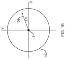
- FIG. 1B an example of such a coordinate system.
- FIG. 1B shows a sectional view of a circular waveguide (e.g., first circular waveguide 102), with the Z axis being the longitudinal axis 104 along which the circular waveguide is disposed, and with X and Y axes that are orthogonal to one another, and orthogonal to the Z axis.
- An electrical field vector 108 is shown at an angle of ⁇ with respect to the X axis, at the point along the Z axis that the section is taken. So in this example, the polarization orientation of the electrical field vector 106 is given by ⁇ , with respect to the X-Y coordinate reference plane.
- the circular waveguide polarization device 100 further includes a second circular waveguide 110, configured to impart a ⁇ /8 relative phase shift between two orthogonal linear polarized signals transmitted at a second polarization orientation.
- the second circular waveguide segment 110 is coaxially adjacent to the first circular waveguide segment along the longitudinal axis 104 to form a waveguide assembly 112.
- the waveguide assembly 112 includes a first end 114 and a second end 116.
- the inside diameter of the first circular waveguide 102 and the second circular waveguide is 0.7 inches, with operating bands of 10.7 to 12.75 GHz and 14 to 14.5 GHz.
- the total length of the waveguide assembly 112 is 5.5 inches.
- the circular waveguide polarization device 100 further includes a waveguide assembly input configured to receive dual linear polarized electromagnetic energy, characterized by a source polarization orientation, from a radiation source 118.
- the radiation source 118 provides first linear polarized electromagnetic energy oriented in a first direction (e.g., in the positive X direction of FIG. 1B ) and second linear polarized electromagnetic energy oriented in a second direction, which is orthogonal to the first linear polarized electromagnet energy (e.g., in the positive Y direction of FIG. 1B ).
- the second end 116 of the waveguide assembly 112 is used as the waveguide assembly input.
- the first end 114 of the waveguide assembly may be used to provide the waveguide assembly input.
- the radiation source 118 is shown at the second end 116 of the waveguide assembly 112 and situated about the longitudinal axis 104, so that dual linear polarized electromagnetic energy is transmitted directly into an end of the waveguide assembly 112 along the longitudinal axis 104.
- the radiation source 118 may be situated in a different location with respect to the waveguide assembly input, and the dual linear polarized electromagnetic energy may be transmitted into the waveguide assembly 112 through alternative paths, for example through a side port or ports of the waveguide assembly 112.
- the first circular waveguide 102 is rotationally orientated about the axis with respect to the second waveguide 110, such that the first polarization orientation is offset by 90 degrees with respect to the second polarization orientation.
- the radiation source 118 is arranged such that the source polarization orientation is 45 degrees with respect to the first polarization orientation and the second polarization orientation. This first operational mode of the waveguide assembly produces circularly polarized radiation.
- the first circular waveguide 102 is rotationally orientated about the longitudinal axis 104 with respect to the second waveguide 110 such that the first polarization orientation and the first polarization orientation are substantially the same.
- the 3 ⁇ /8 phase shift introduced by the first circular waveguide 102 adds to the ⁇ /8 phase shift introduced by the second circular waveguide 110, so that the entire waveguide assembly 112 introduces a ⁇ /2 phase shift.
- a rotation angle of ⁇ is introduced to the linearly polarized signal.
- the waveguide assembly may be configured to rotate about the longitudinal axis 104 to introduce an angular shift to the incoming linearly polarized signal.
- a source circular slip joint 120 may be interposed between the first circular waveguide 102 and the radiation source 118 to facilitate rotation of the waveguide assembly 112 with respect to the radiation source 118, to implement the angular shift described above.
- the rotation may be limited to occur within an angular range of plus or minus ⁇ degrees about the source polarization orientation, where ⁇ is a predetermined angle.
- the rotation may be limited to occur within an angular range of plus or minus 20 degrees about the source polarization orientation, although other predetermined angles may alternatively be used.
- An inter-waveguide slip joint 122 may be included to connect the first circular waveguide to the second circular waveguide.
- the inter-waveguide slip joint 122 may be configured to facilitate rotation of the first waveguide 102 and the second waveguide 110, with respect to one another, about the axis 104.
- the circular waveguide polarization device 100 may include a motor assembly 124 for rotating the waveguide assembly 112 or portions of the waveguide assembly 112 about the axis 104.
- the circular waveguide polarization device 100 may further comprise a motor controller 125, which receives position commands 127 from an external source (not shown) and converts the position commands 127 into control signals 129 suitable for controlling the motor assembly 124.
- the motor controller 125 may include processing components necessary to convert the position commands 127 into control signals 129 and to perform other associated actions.
- the motor assembly 124 may comprise a stepper motor as is known in the art, although in alternative embodiments other types of motors capable of controlling angular position may be used.
- the motor assembly may be configured to independently rotate the first waveguide segment 102 and the second waveguide segment 110, with respect to one another, about the axis 104.
- the motor assembly may comprise a first motor (subsumed within the motor assembly 124; not explicitly shown) arranged to rotate the first circular waveguide 102, and a second motor (subsumed within the motor assembly 124; not explicitly shown) arranged to rotate the second circular waveguide 110 independent of the first circular waveguide 102.
- the motor assembly 124 may comprise a single motor arranged such that when the motor assembly 124 rotates the first circular waveguide 102 and the second circular waveguide 110 in a first direction about the axis 104, the slip joint 122 causes the first circular waveguide 102 and the second circular waveguide 110 to lock together in the first mode of the waveguide assembly 112.
- the slip joint 122 causes the first circular waveguide 102 and the second circular waveguide 110 to lock together in the second mode of the waveguide assembly.
- the slip joint 122 When in the second mode of the waveguide assembly 112, and when the motor assembly 124 rotates in the second direction such that the first polarization orientation and the first polarization orientation is offset by a predetermined angle ⁇ , the slip joint 122 causes the first circular waveguide 102 and the second circular waveguide 110 to unlock.
- the circular waveguide polarization device 100 may further include a feed horn 126 attached to an end of the waveguide assembly 112.
- the circular waveguide polarization device 100 may include a feed horn slip joint 128 coupling the feed horn 126 to the waveguide assembly 112 to allow rotational movement of the feed horn 126 to the waveguide assembly 112 with respect to one another about the axis 104.
- the circular waveguide polarization device 100 operates in a reciprocal nature. Accordingly the circular waveguide polarization device 100 may further include a receiver attached to or otherwise associated with the first end of the waveguide assembly. The receiver may be configured to receive electromagnetic energy, transmitted through the waveguide assembly directed from the second end to the first end, and modified as described herein by the phase shift devices.
- the radiation source 118 and the receiver are described in the example embodiment as being attached to or otherwise associated with an end of the waveguide assembly 112, in some embodiments the radiation source 118 and/or the receiver may be located apart from the waveguide assembly 112.
- the waveguide assembly 112 may have attached or otherwise associated with it an orthomode transducer (OMT) for conveying electromagnetic energy to and/or from the waveguide assembly 112.
- OMT orthomode transducer
- transmission paths such as waveguides may be employed to convey electromagnetic energy between the waveguide assembly 112 and the radiation source and/or receiver.
- FIGs. 2A and 2B illustrate interior components of the circular waveguide polarization device 100 shown in FIG. 1 .
- the first circular waveguide 102 implements the 3 ⁇ /8 phase shift by utilizing a first phase shift device 202 that lies within a plane that intersects the axis 104 and the opposing interior walls of the first waveguide 102.
- the first phase shift device 202 extends to the opposing interior walls of the first waveguide 102 and includes a first end and a second end that terminates the first phase shift device 202 in a direction parallel to the axis 104.
- Each end of the first phase shift device 202 comprises a transition 204 configured to implement an impedance match between the first phase shift device and the first circular waveguide 102.
- the first phase shift device 202 comprises a dielectric material, although for other embodiments the phase shift device may comprise other materials instead of or in addition to dielectric materials.
- the dielectric material may be RO003 produced by Rogers Corporation, with a dielectric constant of 3.55, a loss tangent of 0.0027, and a thickness of 0.032 inches.
- the first phase shift device 202 is a dielectric card 3.5 inches in length
- the second phase shift device is a dielectric card 2.0 inches in length.
- the second circular waveguide 110 implements the ⁇ /8 phase shift with a second phase shift device 206 that lies within a plane that intersects the axis 104 and the opposing interior walls of the second waveguide 110.
- the second phase shift device 206 extends to the opposing interior walls of the first waveguide 102 and includes a first end and a second end that terminates the second phase shift card 206 in a direction parallel to the axis 104.
- Each end of the second phase shift device 206 comprises a transition 208 configured to implement an impedance match between the first phase shift device and the first circular waveguide 102.
- the second phase shift device 206 comprises a dielectric material, although for other embodiments the phase shift device may comprise other materials instead of or in addition to dielectric materials.
- phase shift devices described for the example embodiment are dielectric cards as described above, it should be understood that other techniques for implementing a phase delay may also be used.
- one or more of the phase shift devices of the waveguide assembly 112 may comprise at least one metal ridge inside the circular waveguide.
- FIGs. 3A and 3B illustrate an end-view of an example waveguide assembly 112 configured in the second operational mode described herein (i.e., linear polarization).
- FIG. 3A shows the first phase shift device 202 and the second phase shift device 206 within a common plane, and rotated at an angle of 0° with respect to the electromagnetic radiation source polarization, resulting in a 0° skew angle.
- looking into the first circular waveguide 102 only the first phase shift device 202 can be seen.
- 3B shows the first phase shift device 202 and the second phase shift device 206 within a common plane, and rotated at an angle of ⁇ /2 (e.g., 10°) with respect to the electromagnetic radiation source polarization, resulting in a skew angle of ⁇ (i.e., 20°).
- ⁇ /2 e.g. 10°
- FIG. 4A illustrates a side internal view
- FIG. 4B illustrates an end view, of an example waveguide assembly 112 configured in the first operational mode described herein (i.e., circular polarization), with the first phase shift device 202 and the second phase shift device 206 oriented at 90° with respect to one another.
- FIG. 4A shows the first circular waveguide 102 with the first phase shift device 202 seen edge-on, and the second circular waveguide 110 with the second phase shift device 206 seen spanning the second circular waveguide from sidewall to sidewall.
- FIG. 4B shows an end-view of the waveguide assembly 112, looking into the first circular waveguide 102.
- the source polarization is such that the linearly polarized fields are oriented with respect to the x and y axes shown, such that the first phase shift device 202 and the second phase shift device 206 are oriented at 45° with respect to the source linearly polarized fields.
- FIG. 5 illustrates the reflection levels, also known as return loss levels, for the example linear polarization configuration with both phase cards parallel, as shown in FIGs. 2B , 3A and 3B .
- FIG. 6A shows the transmitted output modes for the example linear polarization configuration with both phase cards parallel, as shown in FIGs. 2B , 3A and 3B , and mode 1 excitation.
- the transmission level for the vertical polarized mode depicted by v_trace 602 is -0.16 dB, i.e., nearly 0.0 dB, when the vertical polarized mode is injected at the input.
- the transmission level for the opposite polarized mode, horizontal polarized mode, depicted by h_trace 604 is -35.5dB when the vertical polarized mode is injected at the input of the waveguide assembly 112.
- Circular waveguides support propagation of two orthogonally polarized dominant waveguide modes.
- the modes are known as TE 11 modes.
- the nomenclature used at the circular waveguide input is Port 1, Mode1 and Port 1, Mode 2.
- the electric field directions of these circular waveguide input modes are exhibited in FIGs. 6B and 6C.
- FIG. 6B illustrates port 1, mode 1, the electric field aligned with the X axis
- FIG. 6C illustrates port 1, mode 2, the electric field aligned with the Y axis.
- FIG. 7 shows the transmitted output modes for the example linear polarization configuration with both phase cards parallel, as shown in FIGs. 2B , 3A and 3B , and mode 2 excitation.
- the transmission level for the horizontal polarized mode, depicted by h_trace 702 is -0.02dB, i.e., nearly 0.0 dB, when the horizontal polarized mode is injected at the input of the waveguide assembly 112.
- the transmission level for the opposite polarized mode, vertical polarized mode, depicted by v_trace 704 is -35.7dB when the horizontal polarized mode is injected at the input of the waveguide assembly 112.
- FIG. 8 shows the transmitted output modes for the example circular polarization configuration, as shown in FIGs. 4A and 4B .
- the transmission level for the vertical polarized mode shown with v_trace 802 varies around -3dB when the vertical polarized mode is injected at the input of the waveguide assembly 112.
- the transmission level for the opposite polarized mode, horizontal polarized mode, shown with v_trace 804 also varies around -3dB when the vertical polarization mode is injected at the input.
- the difference between these two curves represents the axial ratio of the circular polarized output mode. For example, across the transmit Ku-band, between 14.0 and 14.5 GHz, the worst case axial ratio is 0.36dB. Across the receive Ku-band, between 10.70 and 12.75 GHz, the worst case axial ratio is 0.82dB.
- FIG. 9 shows the transmitted phase of the output modes for the example circular polarization configuration, as shown in FIGs. 4A and 4B .
- the difference between these two curves represents the relative phase of the device between the two orthogonal polarization output modes when orientated in the circular polarized configuration.
- the relative phase between the output polarization modes is less than 3.5 degrees from 90 degrees.
- a relative delay of 90 degrees between the output polarization modes results in a pure circular polarized signal for a perfect linear polarized input signal.
- FIG. 10 shows the reflection levels, also known as return loss levels, for the example circular polarization configuration, as shown in FIGs. 4A and 4B .
- the worst-case return loss level for both polarization modes is 30 dB from 10.7 to 14.5GHz.
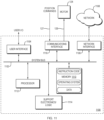
- FIG. 11 is a diagram of an example internal structure of a processing system 1100 that may be used to implement one or more of the embodiments described herein, for example the motor controller 125 described herein with respect to FIG. 1A .
- Each processing system 1100 contains a system bus 1102, where a bus is a set of hardware lines used for data transfer among the components of a computer or processing system.
- the system bus 1102 is essentially a shared conduit that connects different components of a processing system (e.g., processor, disk storage, memory, input/output ports, network ports, etc.) that enables the transfer of information between the components.
- Attached to the system bus 1102 is a user I/O device interface 1104 for connecting various input and output devices (e.g., keyboard, mouse, displays, printers, speakers, etc.) to the processing system 1100.
- a network interface 1106 allows the computer to connect to various other devices attached to a network 1108.
- Memory 1110 provides volatile and non-volatile storage for information such as computer software instructions used to implement one or more of the embodiments of the present invention described herein, for data generated internally and for data received from sources external to the processing system 1100.
- a central processor unit 1112 is also attached to the system bus 1102 and provides for the execution of computer instructions stored in memory 1110.
- the system may also include support electronics/logic 1114, and a communications interface 1116.
- the communications interface may provide control signals 129 to the motor 124, and receive position commands 127, described with reference to FIG. 1A .
- the information stored in memory 1110 may comprise a computer program product, such that the memory 1110 may comprise a non-transitory computer-readable medium (e.g., a removable storage medium such as one or more DVD-ROM's, CD-ROM's, diskettes, tapes, etc.) that provides at least a portion of the software instructions for the invention system.
- the computer program product can be installed by any suitable software installation procedure, as is well known in the art.
- at least a portion of the software instructions may also be downloaded over a cable communication and/or wireless connection.
- certain embodiments of the example embodiments described herein may be implemented as logic that performs one or more functions.
- This logic may be hardware-based, software-based, or a combination of hardware-based and software-based.
- Some or all of the logic may be stored on one or more tangible, non-transitory, computer-readable storage media and may include computer-executable instructions that may be executed by a controller or processor.
- the computer-executable instructions may include instructions that implement one or more embodiments of the invention.
- the tangible, non-transitory, computer-readable storage media may be volatile or non-volatile and may include, for example, flash memories, dynamic memories, removable disks, and non-removable disks.
Description
- Satellite communication systems convey information, between satellites in earth orbit and terrestrially-based transceiver stations, by propagating electromagnetic energy across a wireless radio link. Important components in any radio link communications systems are antennas. An antenna is a component that converts an electromagnetic wave propagating on a transmission line to an electromagnetic wave propagating in free space (transmission), or an electromagnetic wave propagating in free space to an electromagnetic wave propagating on a transmission line (reception).
- Polarization is an important characteristic of propagating electromagnetic waves. Polarization describes the motion through which an electric field vector of an electromagnetic wave points as the electromagnetic wave travels through a point in space. The electric field vector tip can trace a line, circle, or ellipse as the electromagnetic wave passes through the imaginary point in space. In general, these traces are referred to as linear, circular, or elliptical polarization, respectively.
- Polarization is important in many applications, and particularly for antennas. The polarization of the antenna is defined by the field orientation of the electromagnetic wave it radiates when the antenna is transmitting. The polarization characteristic of the antenna is important because, for maximum power transfer between radio links, the transmitting and receiving antennas must be of identical matching polarization states at the same time. If the transmitting and receiving antennas are linear polarized, for example, and if the transmitting antenna is horizontally polarized while the receiving antenna is vertically polarized, then no power would be received. Conversely, if both the transmitting and receiving antennas are horizontally or vertically polarized, then maximum power is received. Because antennas facilitate the transition of electromagnetic energy propagating between free space and a transmission link, polarization is also an important characteristic of all antennas.
- A particular satellite may be configured to receive and transmit electromagnetic energy having a specific polarization, e.g., either linear polarization (LP), or circular polarization (CP). Because a terrestrially-based transceiver station may be required to communicate with different satellites, the terrestrially-based transceiver station may need to be able to receive and transmit microwave energy having different polarizations.
- An advantage of a radio link using circularly polarized microwave energy is that the angular relationship between the transmitting antenna and the receiving antenna is largely irrelevant. For linearly polarized radio links, however, the angular relationship is important because, as described above, the polarization angle of the transmitter must match the polarization angle of the receiver for maximum power transfer.
- For stationary, terrestrially-based transceiver stations, the polarization angle that matches the target satellite may be determined based on the terrestrial location of the transceiver station and the position of the satellite. If the location of the terrestrially-based transceiver station changes, or if the terrestrially-based transceiver stations acquires a different satellite, the polarization angle of the transceiver station may need to change to match the satellite polarization. The ability to change the polarization angle is referred to herein as "polarization skew control."
- Prior art polarization skew control may involve rotating the entire transceiver, which may be heavy and difficult to mechanically move. Further, the rotation may require flexible cables/waveguide assemblies to accommodate the rotation.
- Document
US 2012/169557 A1 discloses a waveguide which has a distal, medial, and proximal sections. The distal and medial sections rotate relative to each other and to the proximal section. In a first configuration, the waveguide transforms linearly polarized electromagnetic radiation at the proximal end of the proximal section to linearly polarized electromagnetic radiation at the distal end of the distal section and vice versa. In a second configuration, the waveguide transforms linearly polarized radiation at the proximal end of the proximal section into circularly polarized electromagnetic radiation at the distal end of the distal section and vice versa. Preferably, the distal and medial sections include respective eight-wavelength polarizers and the proximal section includes a quarter-wavelength polarizer. A multi-band antenna feed includes two such waveguides, one nested inside the other, for transforming electromagnetic radiation of respective frequency bands. - Document
JP S53105157 A - Document
US 2425345 A discloses, in combination, a rectangular guide having a short and a long transverse dimension, a circular guide connected thereto, a device connected to said rectangular guide for supplying to both guides a wave polarized parallel to said short transverse dimension, and means for extracting from the circular guide completely and without reflection the energy in a component derived from said wave and polarized parallel to said long dimension. Said means comprise a member for receiving said component without reflection attached to the wall of the circular guide. The spacing between the longitudinal axis of said member and the junction of said rectangular and circular guides is a fraction of a wavelength as measured in the guide, and a resistance element for absorbing without reflection and dissipating said energy directly connected to said member. Said element extends perpendicular to the longitudinal axis of said circular guide. - Document
US 9257734 B2 -
EP1032069 A1 discloses a waveguide assembly comprising a fixed waveguide section implementing a quarter-wavelength polarizer and two rotatable waveguide sections implementing eighth-wavelength polarizers . - The described embodiments present a circular waveguide polarization device that can provide polarization skew control by switching between two configurations; dual circular polarization, and dual linear polarization with skew control. Some embodiments use a single stepper motor to facilitate the skew control. The described embodiments may be useful in receive only and VSAT marine antennas. The described embodiments may alternatively be used in other applications, for example, as an antenna with polarization switching configurations between low earth orbit (LEO) satellites with circular polarization, and geosynchronous earth orbit (GEO) satellites with linear polarization.
- Another advantage of the described embodiments is that the linear polarization skew is controlled solely by rotation of circular waveguide subassemblies. The orthomode transducer (OMT) and transceiver in the very small aperture terminal (VSAT) case, and the global low noise block downconverter (LNB) in the receive only case, can remained fixed to the back of the antenna reflector. This configuration eliminates the need for extra flexible cables and heavy load bearings to rotate the larger mass behind the reflector vertex.
- In order to create a circular polarization, a ninety degree (90°, or equivalently, λ/4) phase delay is inserted into one linear polarization path of the dual polarized circular waveguide. The delay can be generated, for example, by a dielectric phase card, dielectric pins, metal ridges or metal pins. The phase delay is inserted at 45 degrees (45°, or equivalently, λ/8) relative to the linear polarization of the source. A ninety degree phase delay orientated at 45 degrees to the linear source polarization creates circular polarization.
- In some situations, it is desirable to introduce a fixed amount of angular rotation, along the axis of propagation, to a linearly polarized signal. A rotation angle of φ is introduced to a linearly polarized signal if a 180 degree (180°; λ/2) phase delay is inserted at an angle of φ/2 with respect to the source polarization.
- The claimed invention defines a waveguide device according to any of
claim 1 to 9. - It is further provided an electromagnetic transmission system according to any of claims 9 to 15. The electromagnetic transmission system includes a waveguide device according to
claim 1. - In some embodiments, a feed horn slip joint may be attached to the feed horn and to the waveguide assembly, the feed horn slip joint configured to facilitate rotation, relative to one another, of the feed horn and the waveguide assembly about the axis. The feed horn may be fixedly attached to the waveguide assembly.
- The foregoing will be apparent from the following more particular description of example embodiments of the invention, as illustrated in the accompanying drawings in which like reference characters refer to the same parts throughout the different views. The drawings are not necessarily to scale, emphasis instead being placed upon illustrating embodiments of the present invention.
-
FIG. 1A illustrates an example embodiment of a circular waveguide polarization device according to the invention. -
FIG. 1B shows a sectional view of a circular waveguide of the circular waveguide polarization ofFIG. 1A . -
FIGs. 2A and2B illustrates interior components of the circular waveguide polarization device shown inFIG. 1 . -
FIGs. 3A and 3B illustrate an end-view of an example waveguide assembly configured in the second operational mode of the invention. -
FIGs. 4A and 4B illustrate a side internal view and an end view, respectively, of an example waveguide assembly configured in the first operational mode of the invention. -
FIG. 5 illustrates the reflection levels for the example LP configuration with both phase cards parallel. -
FIG. 6A shows the transmitted output modes for the example LP configuration with both phase cards parallel andmode 1 excitation. -
FIG. 6B illustrates electric field alignment forport 1,mode 1. -
FIG. 6C illustrates electric field alignment forport 1,mode 2. -
FIG. 7 shows the transmitted output modes for the example LP configuration with both phase cards parallel andmode 2 excitation. -
FIG. 8 shows the transmitted output modes for the example CP configuration -
FIG. 9 shows the transmitted phase of the output modes for the example circular polarization configuration. -
FIG. 10 shows the reflection levels for the example circular polarization configuration. -
FIG. 11 is a diagram of an example internal structure of a processing system that may be used to implement one or more of the embodiments. - A description of example embodiments of the invention follows.
- The teachings of all patents, published applications and references cited herein are incorporated by reference in their entirety.
-
FIG. 1A illustrates an example embodiment of a circularwaveguide polarization device 100 constructed and arranged according to the described embodiments. Theexample device 100 comprises a firstcircular waveguide 102 configured to implement a 3λ/8 relative phase shift between two orthogonal linear polarized signals transmitted into the firstcircular waveguide 102 at a first polarization orientation. - As used herein, the "polarization orientation" of a signal refers the angular orientation of the transmitted signal's electrical field vector, with respect to a reference coordinate system.
FIG. 1B an example of such a coordinate system.FIG. 1B shows a sectional view of a circular waveguide (e.g., first circular waveguide 102), with the Z axis being thelongitudinal axis 104 along which the circular waveguide is disposed, and with X and Y axes that are orthogonal to one another, and orthogonal to the Z axis. An electrical field vector 108 is shown at an angle of Φ with respect to the X axis, at the point along the Z axis that the section is taken. So in this example, the polarization orientation of theelectrical field vector 106 is given by Φ, with respect to the X-Y coordinate reference plane. - The circular
waveguide polarization device 100 further includes a secondcircular waveguide 110, configured to impart a λ/8 relative phase shift between two orthogonal linear polarized signals transmitted at a second polarization orientation. The secondcircular waveguide segment 110 is coaxially adjacent to the first circular waveguide segment along thelongitudinal axis 104 to form awaveguide assembly 112. Thewaveguide assembly 112 includes afirst end 114 and asecond end 116. - In an example embodiment, the inside diameter of the first
circular waveguide 102 and the second circular waveguide is 0.7 inches, with operating bands of 10.7 to 12.75 GHz and 14 to 14.5 GHz. The total length of thewaveguide assembly 112 is 5.5 inches. - The circular
waveguide polarization device 100 further includes a waveguide assembly input configured to receive dual linear polarized electromagnetic energy, characterized by a source polarization orientation, from aradiation source 118. In the example embodiment, theradiation source 118 provides first linear polarized electromagnetic energy oriented in a first direction (e.g., in the positive X direction ofFIG. 1B ) and second linear polarized electromagnetic energy oriented in a second direction, which is orthogonal to the first linear polarized electromagnet energy (e.g., in the positive Y direction ofFIG. 1B ). - In the example embodiment of
FIG. 1A , thesecond end 116 of thewaveguide assembly 112 is used as the waveguide assembly input. For alternative embodiments, thefirst end 114 of the waveguide assembly may be used to provide the waveguide assembly input. Also, as depicted inFIG. 1A , theradiation source 118 is shown at thesecond end 116 of thewaveguide assembly 112 and situated about thelongitudinal axis 104, so that dual linear polarized electromagnetic energy is transmitted directly into an end of thewaveguide assembly 112 along thelongitudinal axis 104. In other embodiments, however, theradiation source 118 may be situated in a different location with respect to the waveguide assembly input, and the dual linear polarized electromagnetic energy may be transmitted into thewaveguide assembly 112 through alternative paths, for example through a side port or ports of thewaveguide assembly 112. - For a first operational mode of the
waveguide assembly 112, the firstcircular waveguide 102 is rotationally orientated about the axis with respect to thesecond waveguide 110, such that the first polarization orientation is offset by 90 degrees with respect to the second polarization orientation. Theradiation source 118 is arranged such that the source polarization orientation is 45 degrees with respect to the first polarization orientation and the second polarization orientation. This first operational mode of the waveguide assembly produces circularly polarized radiation. - For a second operational mode of the
waveguide assembly 112, the firstcircular waveguide 102 is rotationally orientated about thelongitudinal axis 104 with respect to thesecond waveguide 110 such that the first polarization orientation and the first polarization orientation are substantially the same. In the configuration of this second mode of thewaveguide assembly 112, the 3λ/8 phase shift introduced by the firstcircular waveguide 102 adds to the λ/8 phase shift introduced by the secondcircular waveguide 110, so that theentire waveguide assembly 112 introduces a λ/2 phase shift. As described herein, when a λ/2 phase delay is inserted in the transmission path of a linearly polarized signal, at an angle of φ/2 with respect to the source polarization, a rotation angle of φ is introduced to the linearly polarized signal. So in the second mode, the waveguide assembly may be configured to rotate about thelongitudinal axis 104 to introduce an angular shift to the incoming linearly polarized signal. - A source circular slip joint 120 may be interposed between the first
circular waveguide 102 and theradiation source 118 to facilitate rotation of thewaveguide assembly 112 with respect to theradiation source 118, to implement the angular shift described above. In some embodiments, the rotation may be limited to occur within an angular range of plus or minus θ degrees about the source polarization orientation, where θ is a predetermined angle. For example, the rotation may be limited to occur within an angular range of plus or minus 20 degrees about the source polarization orientation, although other predetermined angles may alternatively be used. - An inter-waveguide slip joint 122 may be included to connect the first circular waveguide to the second circular waveguide. The inter-waveguide slip joint 122 may be configured to facilitate rotation of the
first waveguide 102 and thesecond waveguide 110, with respect to one another, about theaxis 104. - The circular
waveguide polarization device 100 may include amotor assembly 124 for rotating thewaveguide assembly 112 or portions of thewaveguide assembly 112 about theaxis 104. The circularwaveguide polarization device 100 may further comprise amotor controller 125, which receives position commands 127 from an external source (not shown) and converts the position commands 127 intocontrol signals 129 suitable for controlling themotor assembly 124. Themotor controller 125 may include processing components necessary to convert the position commands 127 intocontrol signals 129 and to perform other associated actions. - The
motor assembly 124 may comprise a stepper motor as is known in the art, although in alternative embodiments other types of motors capable of controlling angular position may be used. In some embodiments, the motor assembly may be configured to independently rotate thefirst waveguide segment 102 and thesecond waveguide segment 110, with respect to one another, about theaxis 104. In such embodiments, the motor assembly may comprise a first motor (subsumed within themotor assembly 124; not explicitly shown) arranged to rotate the firstcircular waveguide 102, and a second motor (subsumed within themotor assembly 124; not explicitly shown) arranged to rotate the secondcircular waveguide 110 independent of the firstcircular waveguide 102. - In other embodiments, the
motor assembly 124 may comprise a single motor arranged such that when themotor assembly 124 rotates the firstcircular waveguide 102 and the secondcircular waveguide 110 in a first direction about theaxis 104, the slip joint 122 causes the firstcircular waveguide 102 and the secondcircular waveguide 110 to lock together in the first mode of thewaveguide assembly 112. When themotor assembly 124 rotates the firstcircular waveguide 102 and secondcircular waveguide 110 about theaxis 104 in a second direction that is opposite to the first direction, the slip joint 122 causes the firstcircular waveguide 102 and the secondcircular waveguide 110 to lock together in the second mode of the waveguide assembly. When in the second mode of thewaveguide assembly 112, and when themotor assembly 124 rotates in the second direction such that the first polarization orientation and the first polarization orientation is offset by a predetermined angle θ, the slip joint 122 causes the firstcircular waveguide 102 and the secondcircular waveguide 110 to unlock. - The circular
waveguide polarization device 100 may further include afeed horn 126 attached to an end of thewaveguide assembly 112. In some embodiments, the circularwaveguide polarization device 100 may include a feed horn slip joint 128 coupling thefeed horn 126 to thewaveguide assembly 112 to allow rotational movement of thefeed horn 126 to thewaveguide assembly 112 with respect to one another about theaxis 104. - The circular
waveguide polarization device 100 operates in a reciprocal nature. Accordingly the circularwaveguide polarization device 100 may further include a receiver attached to or otherwise associated with the first end of the waveguide assembly. The receiver may be configured to receive electromagnetic energy, transmitted through the waveguide assembly directed from the second end to the first end, and modified as described herein by the phase shift devices. - It should be understood that although the
radiation source 118 and the receiver (not shown) are described in the example embodiment as being attached to or otherwise associated with an end of thewaveguide assembly 112, in some embodiments theradiation source 118 and/or the receiver may be located apart from thewaveguide assembly 112. For example, thewaveguide assembly 112 may have attached or otherwise associated with it an orthomode transducer (OMT) for conveying electromagnetic energy to and/or from thewaveguide assembly 112. In such embodiments, transmission paths such as waveguides may be employed to convey electromagnetic energy between thewaveguide assembly 112 and the radiation source and/or receiver. -
FIGs. 2A and2B illustrate interior components of the circularwaveguide polarization device 100 shown inFIG. 1 . The firstcircular waveguide 102 implements the 3λ/8 phase shift by utilizing a firstphase shift device 202 that lies within a plane that intersects theaxis 104 and the opposing interior walls of thefirst waveguide 102. In this example embodiment, the firstphase shift device 202 extends to the opposing interior walls of thefirst waveguide 102 and includes a first end and a second end that terminates the firstphase shift device 202 in a direction parallel to theaxis 104. Each end of the firstphase shift device 202 comprises atransition 204 configured to implement an impedance match between the first phase shift device and the firstcircular waveguide 102. - In one embodiment, the first
phase shift device 202 comprises a dielectric material, although for other embodiments the phase shift device may comprise other materials instead of or in addition to dielectric materials. In an example embodiment, the dielectric material may be RO003 produced by Rogers Corporation, with a dielectric constant of 3.55, a loss tangent of 0.0027, and a thickness of 0.032 inches. For this example embodiment, the firstphase shift device 202 is a dielectric card 3.5 inches in length, and the second phase shift device is a dielectric card 2.0 inches in length. - The second
circular waveguide 110 implements the λ/8 phase shift with a secondphase shift device 206 that lies within a plane that intersects theaxis 104 and the opposing interior walls of thesecond waveguide 110. In this example embodiment, the secondphase shift device 206 extends to the opposing interior walls of thefirst waveguide 102 and includes a first end and a second end that terminates the secondphase shift card 206 in a direction parallel to theaxis 104. Each end of the secondphase shift device 206 comprises atransition 208 configured to implement an impedance match between the first phase shift device and the firstcircular waveguide 102. In one embodiment, the secondphase shift device 206 comprises a dielectric material, although for other embodiments the phase shift device may comprise other materials instead of or in addition to dielectric materials. - While the phase shift devices described for the example embodiment are dielectric cards as described above, it should be understood that other techniques for implementing a phase delay may also be used. For example, one or more of the phase shift devices of the
waveguide assembly 112 may comprise at least one metal ridge inside the circular waveguide. -
FIGs. 3A and 3B illustrate an end-view of anexample waveguide assembly 112 configured in the second operational mode described herein (i.e., linear polarization).FIG. 3A shows the firstphase shift device 202 and the secondphase shift device 206 within a common plane, and rotated at an angle of 0° with respect to the electromagnetic radiation source polarization, resulting in a 0° skew angle. In this example view, looking into the firstcircular waveguide 102, only the firstphase shift device 202 can be seen.FIG. 3B shows the firstphase shift device 202 and the secondphase shift device 206 within a common plane, and rotated at an angle of φ/2 (e.g., 10°) with respect to the electromagnetic radiation source polarization, resulting in a skew angle of φ (i.e., 20°). -
FIG. 4A illustrates a side internal view, andFIG. 4B illustrates an end view, of anexample waveguide assembly 112 configured in the first operational mode described herein (i.e., circular polarization), with the firstphase shift device 202 and the secondphase shift device 206 oriented at 90° with respect to one another.FIG. 4A shows the firstcircular waveguide 102 with the firstphase shift device 202 seen edge-on, and the secondcircular waveguide 110 with the secondphase shift device 206 seen spanning the second circular waveguide from sidewall to sidewall.FIG. 4B shows an end-view of thewaveguide assembly 112, looking into the firstcircular waveguide 102. In this example embodiment, the source polarization is such that the linearly polarized fields are oriented with respect to the x and y axes shown, such that the firstphase shift device 202 and the secondphase shift device 206 are oriented at 45° with respect to the source linearly polarized fields. -
FIG. 5 illustrates the reflection levels, also known as return loss levels, for the example linear polarization configuration with both phase cards parallel, as shown inFIGs. 2B ,3A and 3B . The return losses for the input vertical polarization mode, depicted byv_trace 502, and the input horizontal polarization mode, depicted byh_trace 504, are both shown inFIG. 5 . The worst-case return loss level for both polarization modes, asFIG. 5 shows, is 20 dB from 10.7 to 14.5GHz. -
FIG. 6A shows the transmitted output modes for the example linear polarization configuration with both phase cards parallel, as shown inFIGs. 2B ,3A and 3B , andmode 1 excitation. The transmission level for the vertical polarized mode, depicted byv_trace 602, is -0.16 dB, i.e., nearly 0.0 dB, when the vertical polarized mode is injected at the input. The transmission level for the opposite polarized mode, horizontal polarized mode, depicted byh_trace 604, is -35.5dB when the vertical polarized mode is injected at the input of thewaveguide assembly 112. - Circular waveguides support propagation of two orthogonally polarized dominant waveguide modes. The modes are known as TE11 modes. The nomenclature used at the circular waveguide input is
Port 1, Mode1 andPort 1,Mode 2. The electric field directions of these circular waveguide input modes are exhibited inFIGs. 6B and 6C. FIG. 6B illustratesport 1,mode 1, the electric field aligned with the X axis, andFIG. 6C illustratesport 1,mode 2, the electric field aligned with the Y axis. -
FIG. 7 shows the transmitted output modes for the example linear polarization configuration with both phase cards parallel, as shown inFIGs. 2B ,3A and 3B , andmode 2 excitation. The transmission level for the horizontal polarized mode, depicted byh_trace 702, is -0.02dB, i.e., nearly 0.0 dB, when the horizontal polarized mode is injected at the input of thewaveguide assembly 112. The transmission level for the opposite polarized mode, vertical polarized mode, depicted byv_trace 704, is -35.7dB when the horizontal polarized mode is injected at the input of thewaveguide assembly 112. -
FIG. 8 shows the transmitted output modes for the example circular polarization configuration, as shown inFIGs. 4A and 4B . The transmission level for the vertical polarized mode, shown withv_trace 802, varies around -3dB when the vertical polarized mode is injected at the input of thewaveguide assembly 112. The transmission level for the opposite polarized mode, horizontal polarized mode, shown withv_trace 804, also varies around -3dB when the vertical polarization mode is injected at the input. At any frequency, the difference between these two curves represents the axial ratio of the circular polarized output mode. For example, across the transmit Ku-band, between 14.0 and 14.5 GHz, the worst case axial ratio is 0.36dB. Across the receive Ku-band, between 10.70 and 12.75 GHz, the worst case axial ratio is 0.82dB. -
FIG. 9 shows the transmitted phase of the output modes for the example circular polarization configuration, as shown inFIGs. 4A and 4B . The transmitted phase of the vertical polarized mode, when the vertical polarized mode is injected at the input, is depicted byv_trace 902. The transmitted phase of the opposite polarized mode, the horizontal polarized mode, when the vertical polarization mode is injected at the input of thewaveguide assembly 112, is depicted byh_trace 904. At any frequency, the difference between these two curves represents the relative phase of the device between the two orthogonal polarization output modes when orientated in the circular polarized configuration. For example, across the Ku-band, the relative phase between the output polarization modes is less than 3.5 degrees from 90 degrees. As described herein, a relative delay of 90 degrees between the output polarization modes results in a pure circular polarized signal for a perfect linear polarized input signal. -
FIG. 10 shows the reflection levels, also known as return loss levels, for the example circular polarization configuration, as shown inFIGs. 4A and 4B . The return losses for the input vertical polarization mode, depicted byv_trace 1002, and the input horizontal polarization mode, depicted byh_trace 1004, are both shown in this figure. The worst-case return loss level for both polarization modes is 30 dB from 10.7 to 14.5GHz. -
FIG. 11 is a diagram of an example internal structure of aprocessing system 1100 that may be used to implement one or more of the embodiments described herein, for example themotor controller 125 described herein with respect toFIG. 1A . - Each
processing system 1100 contains asystem bus 1102, where a bus is a set of hardware lines used for data transfer among the components of a computer or processing system. Thesystem bus 1102 is essentially a shared conduit that connects different components of a processing system (e.g., processor, disk storage, memory, input/output ports, network ports, etc.) that enables the transfer of information between the components. - Attached to the
system bus 1102 is a user I/O device interface 1104 for connecting various input and output devices (e.g., keyboard, mouse, displays, printers, speakers, etc.) to theprocessing system 1100. Anetwork interface 1106 allows the computer to connect to various other devices attached to anetwork 1108.Memory 1110 provides volatile and non-volatile storage for information such as computer software instructions used to implement one or more of the embodiments of the present invention described herein, for data generated internally and for data received from sources external to theprocessing system 1100. - A
central processor unit 1112 is also attached to thesystem bus 1102 and provides for the execution of computer instructions stored inmemory 1110. The system may also include support electronics/logic 1114, and acommunications interface 1116. The communications interface may providecontrol signals 129 to themotor 124, and receive position commands 127, described with reference toFIG. 1A . - In one embodiment, the information stored in
memory 1110 may comprise a computer program product, such that thememory 1110 may comprise a non-transitory computer-readable medium (e.g., a removable storage medium such as one or more DVD-ROM's, CD-ROM's, diskettes, tapes, etc.) that provides at least a portion of the software instructions for the invention system. The computer program product can be installed by any suitable software installation procedure, as is well known in the art. In another embodiment, at least a portion of the software instructions may also be downloaded over a cable communication and/or wireless connection. - It will be apparent that one or more embodiments described herein may be implemented in many different forms of software and hardware. Software code and/or specialized hardware used to implement embodiments described herein is not limiting of the embodiments of the invention described herein. Thus, the operation and behavior of embodiments are described without reference to specific software code and/or specialized hardware - it being understood that one would be able to design software and/or hardware to implement the embodiments based on the description herein.
- Further, certain embodiments of the example embodiments described herein may be implemented as logic that performs one or more functions. This logic may be hardware-based, software-based, or a combination of hardware-based and software-based. Some or all of the logic may be stored on one or more tangible, non-transitory, computer-readable storage media and may include computer-executable instructions that may be executed by a controller or processor. The computer-executable instructions may include instructions that implement one or more embodiments of the invention. The tangible, non-transitory, computer-readable storage media may be volatile or non-volatile and may include, for example, flash memories, dynamic memories, removable disks, and non-removable disks.
- While this invention has been particularly shown and described with references to example embodiments thereof, it will be understood by those skilled in the art that various changes in form and details may be made therein without departing from the scope of the invention encompassed by the appended claims.
Claims (15)
- A waveguide device (100), comprising:a first circular waveguide (102) configured to implement a 3λ/8 relative phase shift between transmission of two orthogonal linear polarized signals transmitted at a first polarization orientation;a second circular waveguide (110) configured to impart a λ/8 relative phase shift between transmission of two orthogonal linear polarized signals transmitted at a second polarization orientation, the second circular waveguide (110) coaxially adjacent to the first circular waveguide (102) along an axis (104) to form a waveguide assembly (112), the waveguide device further comprising a radiation source (118) configured to provide dual linear polarized energy, having a source polarization orientation, into the waveguide assembly (112);wherein the 3λ/8 phase shift is implemented in the first circular waveguide (102) with a first phase shift device (202) that lies within a first plane, the first plane intersects the axis (104) and opposing interior walls of the first waveguide (102), the first plane is disposed in the first polarization orientation, andthe λ/8 phase shift is implemented in the second circular waveguide (110) with a second phase shift device (206) that lies within a second plane, the second plane intersects the axis (104) and opposing interior walls of the second waveguide (110), the second plane is disposed in the second polarization orientation;for a first operational mode of the waveguide assembly (112), the first circular waveguide (102) is rotationally orientated about the axis (104) with respect to the second circular waveguide (110) such that the first polarization orientation is offset by 90 degrees with respect to the second polarization orientation, the radiation source (118) arranged such that the source polarization orientation is 45 degrees with respect to the first polarization orientation and the second polarization orientation; andfor a second operational mode of the waveguide assembly (112), the first circular waveguide (102) is rotationally orientated about the axis (104) with respect to the second circular waveguide (110) such that the first polarization orientation and the second polarization orientation are substantially the same.
- The waveguide device (100) of claim 1, wherein in the second operational mode, the waveguide assembly (112) is configured to rotate within an angular range of plus or minus θ degrees about the source polarization orientation, where θ is a predetermined angle.
- The waveguide device (100) of claims 1 or 2, further including a slip joint (122) arranged to connect the first circular waveguide (102) to the second circular waveguide (110), the slip joint (122) configured to facilitate rotation of the first circular waveguide (102) and the second circular waveguide (110) with respect to one another about the axis (104).
- The waveguide device (100) of claim 3, further including a motor assembly (124) for independently rotating the first circular waveguide (102) and the second circular waveguide (110) about the axis (104),wherein the motor assembly (124) optionally comprises a first motor arranged to rotate the first circular waveguide (102), and a second motor arranged to rotate the second circular waveguide (110) independent of the first circular waveguide (102),wherein the motor assembly (124) optionally further comprises a motor arranged such that:(i) the slip joint (122) is configured to lock together the first circular waveguide (102) and the second circular waveguide (110) in the first operational mode of the waveguide assembly (112) when the motor rotates the first and second circular waveguides in a first direction about the axis (104);(ii) the slip joint (122) is configured to lock together the first circular waveguide (102) and the second circular waveguide (110) in the second operational mode of the waveguide assembly (112) when the motor rotates the first and second circular waveguides about the axis (104) in a second direction that is opposite to the first direction; and(iii) when in the second operational mode of the waveguide assembly (112), the slip joint (122) is configured to unlock the first circular waveguide (102) and the second circular waveguide (110) when the motor rotates in the second direction such that the first polarization orientation and the second polarization orientation is offset by a predetermined angle.
- The waveguide device (100) of claim 3, further including a radiation source slip joint (120) arranged to connect the radiation source (118) to an end of the waveguide assembly, the radiation source slip joint (120) configured to facilitate rotation of the radiation source (118) and the waveguide assembly (112) with respect to one another about the axis (104).
- The waveguide device (100) of any of claims 1-5, further including a feed horn (126) attached to an end of the waveguide assembly (112).
- The waveguide device (100) of any of claims 1-6,wherein the first phase shift device (202) (i) extends to the opposing interior walls of the first circular waveguide (102) and (ii) includes a first end and a second end that terminates the first phase shift device (202) in a direction parallel to the axis (104), each end of the first phase shift device (202) comprises a transition (208) configured to implement an impedance match between the first phase shift device (202) and the first circular waveguide (102),wherein the first phase shift device (202) optionally further comprises a dielectric material.
- The waveguide device (100) of any of claims 1-7,wherein the second phase shift (206) device (i) extends to the opposing interior walls of the second circular waveguide (110) and (ii) includes a first end and a second end that terminates the second phase shift device (206) in a direction parallel to the axis (104), each end of the second phase shift device (206) comprises a transition (208) configured to implement an impedance match between the second phase shift device (206) and the second circular waveguide (110),wherein the second phase shift device (206) optionally further comprises a dielectric material.
- An electromagnetic transmission system including a waveguide device (100) according to claim 1,the first circular waveguide (102) being disposed along the axis (104), the first circular waveguide (102) comprising a first waveguide interior wall at a radius from the axis (104), a first waveguide first end and a first waveguide second end;the second circular waveguide (110) being disposed along the axis (104), the second circular waveguide (110) comprising a second waveguide interior wall at the radius from the axis (104), a second waveguide first end and a second waveguide second end;the 3λ/8 phase shift device being disposed within the first circular waveguide (102) along the axis (104),the λ/8 phase shift device being disposed within the second circular waveguide (110) along the axis (104); the system further comprisinga slip joint (122) attached to the first waveguide first end and the second waveguide second end to form the waveguide assembly (112), the slip joint configured to facilitate rotation of the first circular waveguide (102) and the second circular waveguide (110) with respect to one another about the axis (104):a radiation source (118) arranged to provide dual polarized energy into the waveguide assembly (112);a radiation source slip joint (120) arranged to connect the radiation source (118) to a first end (114) of the waveguide assembly (112), the radiation source slip joint configured to facilitate rotation of the radiation source (118) and the waveguide assembly (112) with respect to one another about the axis (104);a feed horn (126) attached to a second end (116) of the waveguide assembly (112);in the first operational mode of the waveguide assembly (112), the first circular waveguide (102) is axially orientated with respect to the second circular waveguide (110) such that the first plane is rotationally positioned about the axis (104) by ninety degrees with respect to the second plane, and the first plane and the second plane are each positioned forty five degrees with respect to an orientation of the radiation source (118); andin the second operational mode of the waveguide assembly (112), the first circular waveguide (102) is axially orientated with respect to the second circular waveguide (110), such that the first plane and the second plane are coplanar, and the first plane and the second plane are each positioned θ degrees with respect to the radiation source (118), where θ is a predetermined angle.
- The electromagnetic transmission system of claim 9, further including a motor assembly (124) for independently rotating the first circular waveguide (102) and the second circular waveguide (110) about the axis (104),wherein the motor assembly (124) optionally comprises a first motor arranged to rotate the first circular waveguide (102), and a second motor arranged to rotate the second circular waveguide (110),wherein the motor assembly (124) optionally further comprises a motor arranged such that:(i) the slip joint (122) is configured to lock together the first circular waveguide (102) and the second circular waveguide (110) to lock together in the first mode of the waveguide assembly (112) when the motor rotates the first and second circular waveguides in a first direction about the axis (104);(ii) the slip joint is configured to lock together (122) the first circular waveguide (102) and the second circular waveguide (110) in the second mode of the waveguide assembly (112) when the motor rotates the first and second circular waveguides about the axis (104) in a second direction that is opposite to the first direction; and(iii) when in the second mode of the waveguide assembly (112), the slip joint (122) is configured to unlock the first circular waveguide (102) and the second circular waveguide (110) when the motor rotates in the second direction such that the first polarization orientation and the first polarization orientation is offset by a predetermined angle.
- The electromagnetic transmission system of any of claims 9 and 10, wherein the 3λ/8 phase shift device and the λ/8 phase shift device each comprises a dielectric material, wherein the 3 λ/8 phase shift device and the λ/8 phase shift device each optionally comprise at least one metal ridge inside the circular waveguide.
- The electromagnetic transmission system of any of claims 9-11, wherein the 3λ/8 phase shift device extends to the opposing interior walls of the first circular waveguide (102) and includes a first end and a second end that terminates the 3λ/8 phase shift device in a direction parallel to the axis (104), each of the first end and the second end further comprises a transition (208) configured to implement an impedance match between the 3λ/8 phase shift device and the first circular waveguide (102)
- The electromagnetic transmission system of any of claims 9-11, wherein the λ/8 phase shift device extends to the opposing interior walls of the second circular waveguide (110) and includes a first end and a second end that terminates the λ/8 phase shift device in a direction parallel to the axis (104), each of the first end and the second end further comprises a transition (208) configured to implement an impedance match between the λ/8 phase shift device and the second circular waveguide (110).
- The electromagnetic transmission system of any of claims 9-13, further including a feed horn slip joint (128) attached to the feed horn (126) and to the waveguide assembly (112), the feed horn slip joint (128) configured to facilitate rotation, relative to one another, of the feed horn (126) and the waveguide assembly (112) about the axis (104), wherein the feed horn (126) is optionally fixedly attached to the waveguide assembly (112).
- The electromagnetic transmission system of any of claims 9-14, further including a receiver associated with the first end (114) of the waveguide assembly (112), the receiver configured to receive electromagnetic energy transmitted through the waveguide assembly (112) directed from the second end of the waveguide assembly (116) to the first end (114).
Applications Claiming Priority (2)
| Application Number | Priority Date | Filing Date | Title |
|---|---|---|---|
| US15/606,130 US9939585B1 (en) | 2017-05-26 | 2017-05-26 | Waveguide device with switchable polarization configurations |
| PCT/US2018/025651 WO2018217312A1 (en) | 2017-05-26 | 2018-04-02 | Waveguide device with switchable polarization configurations |
Publications (2)
| Publication Number | Publication Date |
|---|---|
| EP3631891A1 EP3631891A1 (en) | 2020-04-08 |
| EP3631891B1 true EP3631891B1 (en) | 2023-06-21 |
Family
ID=61801246
Family Applications (1)
| Application Number | Title | Priority Date | Filing Date |
|---|---|---|---|
| EP18719378.4A Active EP3631891B1 (en) | 2017-05-26 | 2018-04-02 | Waveguide device with switchable polarization configurations |
Country Status (6)
| Country | Link |
|---|---|
| US (1) | US9939585B1 (en) |
| EP (1) | EP3631891B1 (en) |
| JP (1) | JP7101197B2 (en) |
| KR (1) | KR20200012909A (en) |
| CN (1) | CN110692165A (en) |
| WO (1) | WO2018217312A1 (en) |
Families Citing this family (5)
| Publication number | Priority date | Publication date | Assignee | Title |
|---|---|---|---|---|
| US10756417B2 (en) * | 2017-12-14 | 2020-08-25 | Waymo Llc | Adaptive polarimetric radar architecture for autonomous driving |
| EP3561947A1 (en) * | 2018-04-25 | 2019-10-30 | Rosenberger Hochfrequenztechnik GmbH & Co. KG | Polariser for a waveguide and system for transmitting high-frequency electromagnetic signals |
| US11804658B2 (en) * | 2018-11-09 | 2023-10-31 | Hughes Network Systems, Llc | Mitigation of polarization mismatch between reflector and feed antennas by feed predistortion |
| FR3094575B1 (en) * | 2019-03-28 | 2022-04-01 | Swissto12 Sa | Radiofrequency component comprising one or more waveguide devices fitted with ridges |
| WO2022198523A1 (en) * | 2021-03-24 | 2022-09-29 | 北京小米移动软件有限公司 | Information transmission method and apparatus, communication device, and storage medium |
Citations (5)
| Publication number | Priority date | Publication date | Assignee | Title |
|---|---|---|---|---|
| US2425345A (en) * | 1942-12-23 | 1947-08-12 | Bell Telephone Labor Inc | Microwave transmission system |
| JPS5826844B2 (en) * | 1977-02-24 | 1983-06-06 | 三菱電機株式会社 | variable phase attenuator |
| EP0196081B1 (en) * | 1985-03-27 | 1993-08-11 | SELENIA SPAZIO S.p.A. | Device for the combination without r.f. power loss of two or more microwave transmitters running in parallel and without any power ratio |
| EP1032069A1 (en) * | 1999-02-22 | 2000-08-30 | Hughes Electronics Corporation | Reconfigurable polarizer |
| US9257734B2 (en) * | 2013-12-23 | 2016-02-09 | Honeywell International Inc. | Compact amplitude and phase trimmer |
Family Cites Families (17)
| Publication number | Priority date | Publication date | Assignee | Title |
|---|---|---|---|---|
| US2881398A (en) | 1953-05-14 | 1959-04-07 | Thompson Prod Inc | Wave-guide system |
| US2857575A (en) * | 1953-06-22 | 1958-10-21 | Gen Precision Lab Inc | Microwave energy orienter |
| US3215957A (en) | 1962-03-05 | 1965-11-02 | Bendix Corp | Variable polarization for microwaves |
| US3728644A (en) | 1971-11-01 | 1973-04-17 | Bell Telephone Labor Inc | Polarization transformation apparatus |
| JPS56136003A (en) * | 1980-03-27 | 1981-10-23 | Mitsubishi Electric Corp | Antenna device |
| US4606605A (en) * | 1984-06-29 | 1986-08-19 | At&T Bell Laboratories | Optical fiber having in-line polarization filter |
| JPH02260901A (en) * | 1989-03-31 | 1990-10-23 | Kyocera Corp | Circularly polarized wave generator |
| KR100241660B1 (en) * | 1997-05-22 | 2000-03-02 | 서원석 | Fiber polarization control device |
| US20110057849A1 (en) | 2009-09-08 | 2011-03-10 | Orbit Communication Ltd. | Dynamic polarization adjustment for a ground station antenna |
| US8994473B2 (en) | 2010-12-30 | 2015-03-31 | Orbit Communication Ltd. | Multi-band feed assembly for linear and circular polarization |
| KR101166728B1 (en) * | 2011-01-27 | 2012-07-19 | (주)인텔리안테크놀로지스 | Polarizer rotating device for multi polarization and equipment for receiving satellite signal having the same |
| KR101172437B1 (en) * | 2011-03-09 | 2012-08-08 | (주)인텔리안테크놀로지스 | Satellite vsat antenna for transmitting/receiving multi polarization |
| US9203162B2 (en) | 2011-03-09 | 2015-12-01 | Thrane & Thrane A/S | Device for switching between linear and circular polarization using a rotatable depolarizer |
| US8723747B2 (en) * | 2012-03-20 | 2014-05-13 | Kvh Industries, Inc. | Polarization phase device and a feed assembly using the same in the antenna system |
| US9966648B2 (en) * | 2012-08-27 | 2018-05-08 | Kvh Industries, Inc. | High efficiency agile polarization diversity compact miniaturized multi-frequency band antenna system with integrated distributed transceivers |
| CN203871473U (en) * | 2014-05-12 | 2014-10-08 | 北京航天控制仪器研究所 | Dual-mode antenna feed source for mobile carrier satellite communication system |
| CN104064875B (en) * | 2014-07-02 | 2016-04-20 | 南京理工大学 | A kind of W-waveband circularly-polarizedhorn horn antenna of waveguide type |
-
2017
- 2017-05-26 US US15/606,130 patent/US9939585B1/en active Active
-
2018
- 2018-04-02 CN CN201880033965.7A patent/CN110692165A/en active Pending
- 2018-04-02 EP EP18719378.4A patent/EP3631891B1/en active Active
- 2018-04-02 JP JP2019564494A patent/JP7101197B2/en active Active
- 2018-04-02 WO PCT/US2018/025651 patent/WO2018217312A1/en active Application Filing
- 2018-04-02 KR KR1020197037873A patent/KR20200012909A/en not_active Application Discontinuation
Patent Citations (5)
| Publication number | Priority date | Publication date | Assignee | Title |
|---|---|---|---|---|
| US2425345A (en) * | 1942-12-23 | 1947-08-12 | Bell Telephone Labor Inc | Microwave transmission system |
| JPS5826844B2 (en) * | 1977-02-24 | 1983-06-06 | 三菱電機株式会社 | variable phase attenuator |
| EP0196081B1 (en) * | 1985-03-27 | 1993-08-11 | SELENIA SPAZIO S.p.A. | Device for the combination without r.f. power loss of two or more microwave transmitters running in parallel and without any power ratio |
| EP1032069A1 (en) * | 1999-02-22 | 2000-08-30 | Hughes Electronics Corporation | Reconfigurable polarizer |
| US9257734B2 (en) * | 2013-12-23 | 2016-02-09 | Honeywell International Inc. | Compact amplitude and phase trimmer |
Also Published As
| Publication number | Publication date |
|---|---|
| JP2020528226A (en) | 2020-09-17 |
| EP3631891A1 (en) | 2020-04-08 |
| US9939585B1 (en) | 2018-04-10 |
| KR20200012909A (en) | 2020-02-05 |
| WO2018217312A1 (en) | 2018-11-29 |
| CN110692165A (en) | 2020-01-14 |
| JP7101197B2 (en) | 2022-07-14 |
Similar Documents
| Publication | Publication Date | Title |
|---|---|---|
| EP3631891B1 (en) | Waveguide device with switchable polarization configurations | |
| US8963790B2 (en) | Universal microwave waveguide joint and mechanically steerable microwave transmitter | |
| US9537212B2 (en) | Antenna array system for producing dual circular polarization signals utilizing a meandering waveguide | |
| KR101172437B1 (en) | Satellite vsat antenna for transmitting/receiving multi polarization | |
| US9297893B2 (en) | Antenna system | |
| EP3635811B1 (en) | Microwave circular polarizer | |
| US20110057849A1 (en) | Dynamic polarization adjustment for a ground station antenna | |
| EP1024551A2 (en) | Isolation improvement circuit for a dual-polarization antenna | |
| US10044083B2 (en) | Dual-channel polarization correction | |
| US4821046A (en) | Dual band feed system | |
| Abdelaal et al. | Asymmetric compact OMT for X-band SAR applications | |
| US9136607B2 (en) | Antenna beam steering through waveguide mode mixing | |
| KR101067173B1 (en) | Yagi-Uda antenna having CPS feed line | |
| US3815136A (en) | Coaxial tracking signal coupler for antenna feed horn | |
| CN109473774B (en) | Novel dual polarized antenna | |
| US5463358A (en) | Multiple channel microwave rotary polarizer | |
| US6222492B1 (en) | Dual coaxial feed for tracking antenna | |
| US20120146866A1 (en) | Wireless communication antenna device | |
| US10403982B2 (en) | Dual-mode antenna array system | |
| JP2000349535A (en) | Primary radiator | |
| Shu et al. | A High-Gain Antenna with Dual Circular Polarization for W-band mmWave Wireless Communications | |
| JP3058007B2 (en) | Antenna feeder | |
| US5216433A (en) | Polarimetric antenna | |
| RU2802763C1 (en) | Irradiating system of a tracking mirror antenna | |
| WO2021215161A1 (en) | Multimode waveguide antenna |
Legal Events
| Date | Code | Title | Description |
|---|---|---|---|
| STAA | Information on the status of an ep patent application or granted ep patent |
Free format text: STATUS: UNKNOWN |
|
| STAA | Information on the status of an ep patent application or granted ep patent |
Free format text: STATUS: THE INTERNATIONAL PUBLICATION HAS BEEN MADE |
|
| PUAI | Public reference made under article 153(3) epc to a published international application that has entered the european phase |
Free format text: ORIGINAL CODE: 0009012 |
|
| STAA | Information on the status of an ep patent application or granted ep patent |
Free format text: STATUS: REQUEST FOR EXAMINATION WAS MADE |
|
| 17P | Request for examination filed |
Effective date: 20200102 |
|
| AK | Designated contracting states |
Kind code of ref document: A1 Designated state(s): AL AT BE BG CH CY CZ DE DK EE ES FI FR GB GR HR HU IE IS IT LI LT LU LV MC MK MT NL NO PL PT RO RS SE SI SK SM TR |
|
| AX | Request for extension of the european patent |
Extension state: BA ME |
|
| DAV | Request for validation of the european patent (deleted) | ||
| DAX | Request for extension of the european patent (deleted) | ||
| STAA | Information on the status of an ep patent application or granted ep patent |
Free format text: STATUS: EXAMINATION IS IN PROGRESS |
|
| 17Q | First examination report despatched |
Effective date: 20210326 |
|
| GRAP | Despatch of communication of intention to grant a patent |
Free format text: ORIGINAL CODE: EPIDOSNIGR1 |
|
| RIC1 | Information provided on ipc code assigned before grant |
Ipc: H01P 1/17 20060101ALI20221130BHEP Ipc: H01Q 13/02 20060101ALI20221130BHEP Ipc: H01Q 15/24 20060101ALI20221130BHEP Ipc: H01P 1/06 20060101ALI20221130BHEP Ipc: H01P 1/161 20060101AFI20221130BHEP |
|
| STAA | Information on the status of an ep patent application or granted ep patent |
Free format text: STATUS: GRANT OF PATENT IS INTENDED |
|
| INTG | Intention to grant announced |
Effective date: 20230105 |
|
| GRAS | Grant fee paid |
Free format text: ORIGINAL CODE: EPIDOSNIGR3 |
|
| GRAA | (expected) grant |
Free format text: ORIGINAL CODE: 0009210 |
|
| STAA | Information on the status of an ep patent application or granted ep patent |
Free format text: STATUS: THE PATENT HAS BEEN GRANTED |
|
| AK | Designated contracting states |
Kind code of ref document: B1 Designated state(s): AL AT BE BG CH CY CZ DE DK EE ES FI FR GB GR HR HU IE IS IT LI LT LU LV MC MK MT NL NO PL PT RO RS SE SI SK SM TR |
|
| REG | Reference to a national code |
Ref country code: CH Ref legal event code: EP |
|
| REG | Reference to a national code |
Ref country code: DE Ref legal event code: R096 Ref document number: 602018052081 Country of ref document: DE |
|
| REG | Reference to a national code |
Ref country code: AT Ref legal event code: REF Ref document number: 1581574 Country of ref document: AT Kind code of ref document: T Effective date: 20230715 |
|
| REG | Reference to a national code |
Ref country code: IE Ref legal event code: FG4D |
|
| REG | Reference to a national code |
Ref country code: LT Ref legal event code: MG9D |
|
| REG | Reference to a national code |
Ref country code: NL Ref legal event code: MP Effective date: 20230621 |
|
| PG25 | Lapsed in a contracting state [announced via postgrant information from national office to epo] |
Ref country code: SE Free format text: LAPSE BECAUSE OF FAILURE TO SUBMIT A TRANSLATION OF THE DESCRIPTION OR TO PAY THE FEE WITHIN THE PRESCRIBED TIME-LIMIT Effective date: 20230621 Ref country code: NO Free format text: LAPSE BECAUSE OF FAILURE TO SUBMIT A TRANSLATION OF THE DESCRIPTION OR TO PAY THE FEE WITHIN THE PRESCRIBED TIME-LIMIT Effective date: 20230921 |
|
| REG | Reference to a national code |
Ref country code: AT Ref legal event code: MK05 Ref document number: 1581574 Country of ref document: AT Kind code of ref document: T Effective date: 20230621 |
|
| PG25 | Lapsed in a contracting state [announced via postgrant information from national office to epo] |
Ref country code: RS Free format text: LAPSE BECAUSE OF FAILURE TO SUBMIT A TRANSLATION OF THE DESCRIPTION OR TO PAY THE FEE WITHIN THE PRESCRIBED TIME-LIMIT Effective date: 20230621 Ref country code: NL Free format text: LAPSE BECAUSE OF FAILURE TO SUBMIT A TRANSLATION OF THE DESCRIPTION OR TO PAY THE FEE WITHIN THE PRESCRIBED TIME-LIMIT Effective date: 20230621 Ref country code: LV Free format text: LAPSE BECAUSE OF FAILURE TO SUBMIT A TRANSLATION OF THE DESCRIPTION OR TO PAY THE FEE WITHIN THE PRESCRIBED TIME-LIMIT Effective date: 20230621 Ref country code: LT Free format text: LAPSE BECAUSE OF FAILURE TO SUBMIT A TRANSLATION OF THE DESCRIPTION OR TO PAY THE FEE WITHIN THE PRESCRIBED TIME-LIMIT Effective date: 20230621 Ref country code: HR Free format text: LAPSE BECAUSE OF FAILURE TO SUBMIT A TRANSLATION OF THE DESCRIPTION OR TO PAY THE FEE WITHIN THE PRESCRIBED TIME-LIMIT Effective date: 20230621 Ref country code: GR Free format text: LAPSE BECAUSE OF FAILURE TO SUBMIT A TRANSLATION OF THE DESCRIPTION OR TO PAY THE FEE WITHIN THE PRESCRIBED TIME-LIMIT Effective date: 20230922 |
|
| PG25 | Lapsed in a contracting state [announced via postgrant information from national office to epo] |
Ref country code: FI Free format text: LAPSE BECAUSE OF FAILURE TO SUBMIT A TRANSLATION OF THE DESCRIPTION OR TO PAY THE FEE WITHIN THE PRESCRIBED TIME-LIMIT Effective date: 20230621 |
|
| PG25 | Lapsed in a contracting state [announced via postgrant information from national office to epo] |
Ref country code: SK Free format text: LAPSE BECAUSE OF FAILURE TO SUBMIT A TRANSLATION OF THE DESCRIPTION OR TO PAY THE FEE WITHIN THE PRESCRIBED TIME-LIMIT Effective date: 20230621 |
|
| PG25 | Lapsed in a contracting state [announced via postgrant information from national office to epo] |
Ref country code: ES Free format text: LAPSE BECAUSE OF FAILURE TO SUBMIT A TRANSLATION OF THE DESCRIPTION OR TO PAY THE FEE WITHIN THE PRESCRIBED TIME-LIMIT Effective date: 20230621 |
|
| PG25 | Lapsed in a contracting state [announced via postgrant information from national office to epo] |
Ref country code: IS Free format text: LAPSE BECAUSE OF FAILURE TO SUBMIT A TRANSLATION OF THE DESCRIPTION OR TO PAY THE FEE WITHIN THE PRESCRIBED TIME-LIMIT Effective date: 20231021 |
|
| PG25 | Lapsed in a contracting state [announced via postgrant information from national office to epo] |
Ref country code: SM Free format text: LAPSE BECAUSE OF FAILURE TO SUBMIT A TRANSLATION OF THE DESCRIPTION OR TO PAY THE FEE WITHIN THE PRESCRIBED TIME-LIMIT Effective date: 20230621 Ref country code: SK Free format text: LAPSE BECAUSE OF FAILURE TO SUBMIT A TRANSLATION OF THE DESCRIPTION OR TO PAY THE FEE WITHIN THE PRESCRIBED TIME-LIMIT Effective date: 20230621 Ref country code: RO Free format text: LAPSE BECAUSE OF FAILURE TO SUBMIT A TRANSLATION OF THE DESCRIPTION OR TO PAY THE FEE WITHIN THE PRESCRIBED TIME-LIMIT Effective date: 20230621 Ref country code: PT Free format text: LAPSE BECAUSE OF FAILURE TO SUBMIT A TRANSLATION OF THE DESCRIPTION OR TO PAY THE FEE WITHIN THE PRESCRIBED TIME-LIMIT Effective date: 20231023 Ref country code: IS Free format text: LAPSE BECAUSE OF FAILURE TO SUBMIT A TRANSLATION OF THE DESCRIPTION OR TO PAY THE FEE WITHIN THE PRESCRIBED TIME-LIMIT Effective date: 20231021 Ref country code: ES Free format text: LAPSE BECAUSE OF FAILURE TO SUBMIT A TRANSLATION OF THE DESCRIPTION OR TO PAY THE FEE WITHIN THE PRESCRIBED TIME-LIMIT Effective date: 20230621 Ref country code: EE Free format text: LAPSE BECAUSE OF FAILURE TO SUBMIT A TRANSLATION OF THE DESCRIPTION OR TO PAY THE FEE WITHIN THE PRESCRIBED TIME-LIMIT Effective date: 20230621 Ref country code: CZ Free format text: LAPSE BECAUSE OF FAILURE TO SUBMIT A TRANSLATION OF THE DESCRIPTION OR TO PAY THE FEE WITHIN THE PRESCRIBED TIME-LIMIT Effective date: 20230621 Ref country code: AT Free format text: LAPSE BECAUSE OF FAILURE TO SUBMIT A TRANSLATION OF THE DESCRIPTION OR TO PAY THE FEE WITHIN THE PRESCRIBED TIME-LIMIT Effective date: 20230621 |
|
| PG25 | Lapsed in a contracting state [announced via postgrant information from national office to epo] |
Ref country code: PL Free format text: LAPSE BECAUSE OF FAILURE TO SUBMIT A TRANSLATION OF THE DESCRIPTION OR TO PAY THE FEE WITHIN THE PRESCRIBED TIME-LIMIT Effective date: 20230621 |